This chapter describes how the Stratix® IV device digital signal processing (DSP) blocks are optimized to support DSP applications requiring high data throughput, such as finite impulse response (FIR) filters, infinite impulse response (IIR) filters, fast Fourier transform (FFT) functions, and encoders. You can configure the DSP blocks to implement one of several operational modes to suit your application. The built-in shift register chain, multipliers, and adders/subtractors minimize the amount of external logic to implement these functions, resulting in efficient resource usage and improved performance and data throughput for DSP applications.
Many complex systems, such as WiMAX, 3GPP WCDMA, high-performance computing (HPC), voice over Internet protocol (VoIP), H.264 video compression, medical imaging, and HDTV use sophisticated digital signal processing techniques, which typically require a large number of mathematical computations. Stratix IV devices are ideally suited for these tasks because the DSP blocks consist of a combination of dedicated elements that perform multiplication, addition, subtraction, accumulation, summation, and dynamic shift operations.
Along with the high-performance Stratix IV soft logic fabric and TriMatrix memory structures, you can configure DSP blocks to build sophisticated fixed-point and floating-point arithmetic functions. These can be manipulated easily to implement common, larger computationally intensive subsystems such as FIR filters, complex FIR filters, IIR filters, FFT functions, and discrete cosine transform (DCT) functions.
This chapter contains the following sections:
■ “Stratix IV DSP Block Overview” on page 4–2
■ “Stratix IV Simplified DSP Operation” on page 4–4
■ “Stratix IV Operational Modes Overview” on page 4–8
■ “Stratix IV DSP Block Resource Descriptions” on page 4–9
■ “Stratix IV Operational Mode Descriptions” on page 4–15
■ “Software Support” on page 4–35
Subscribe
IA, CYCLONE, HARDCOPY, MAX, MEGACORE, NIOS, QUARTUS and STRATIX are Reg. U.S. Pat. & Tm. Off. countries. All other trademarks and service marks are the property of their respective holders as described at
ance of its semiconductor products to current specifications in accordance with Altera’s standard warranty, but at any time without notice. Altera assumes no responsibility or liability arising out of the application or use of any ressly agreed to in writing by Altera. Altera customers are advised to obtain the latest version of device before placing orders for products or services.
4–2 Chapter 4: DSP Blocks in Stratix IV DevicesStratix IV DSP Block Overview
ier r
8 ers
Stratix IV DSP Block OverviewEach Stratix IV device has two to seven columns of DSP blocks that implement multiplication, multiply-add, multiply-accumulate (MAC), and dynamic shift functions efficiently. Architectural highlights of the Stratix IV DSP block include:
■ High-performance, power optimized, fully registered, and pipelined multiplication operations
■ Natively supported 9-, 12-, 18-, and 36-bit wordlengths
■ Efficiently supported floating-point arithmetic formats (24-bit for single precision and 53-bit for double precision)
■ Signed and unsigned input support
■ Built-in addition, subtraction, and accumulation units to combine multiplication results efficiently
■ Cascading 18-bit input bus to form the tap-delay line for filtering applications
■ Cascading 44-bit output bus to propagate output results from one block to the next block without external logic support
■ Rich and flexible arithmetic rounding and saturation units
■ Efficient barrel shifter support
■ Loopback capability to support adaptive filtering
Table 4–1 lists the number of DSP blocks for the Stratix IV device family.
Table 4–1. Number of DSP Blocks in Stratix IV Devices (Part 1 of 2)
Family Device
DSP
Bloc
ks Independent Input and Output Multiplication OperatorsHigh-Precision
Multiplier Adder Mode
FourMultipl
AddeMode
9 × 9 Multipliers
12 × 12 Multipliers
18 × 18 Multipliers
18 × 18 Complex
36 × 36 Multipliers
18 × 36 Multipliers
18 × 1Multipli
Stratix IV E
EP4SE230 161 1,288 966 644 322 322 644 1288
EP4SE360 130 1,040 780 520 260 260 520 1040
EP4SE530 128 1,024 768 512 256 256 512 1024
EP4SE820 120 960 720 480 240 240 480 960
Stratix IV GX
EP4SGX70 48 384 288 192 96 96 192 384
EP4SGX110 64 512 384 256 128 128 256 512
EP4SGX180 115 920 690 460 230 230 460 920
EP4SGX230 161 1,288 966 644 322 322 644 1288
EP4SGX290 104 832 624 416 208 208 416 832
EP4SGX360 (1) 130 1,040 780 520 260 260 520 1,040
EP4SGX360 (2) 128 1,024 768 512 256 256 512 1,024
EP4SGX530 128 1,024 768 512 256 256 512 1,024
Stratix IV Device Handbook Volume 1 February 2011 Altera Corporation
Chapter 4: DSP Blocks in Stratix IV Devices 4–3Stratix IV DSP Block Overview
ier r
8 ers
Table 4–1 shows that the largest Stratix IV DSP-centric device provides up to 1288 18 × 18 multiplier functionality in the 36 × 36, complex 18 × 18, and summation modes.
Each DSP block occupies four LABs in height and can be divided further into two half blocks that share some common clock signals, but are for all common purposes identical in functionality. Figure 4–1 shows the layout of each DSP block.
Stratix IV GT
EP4S40G2 161 1,288 966 644 322 322 644 1,288
EP4S40G5 128 1,024 768 512 256 256 512 1,024
EP4S100G2 161 1,288 966 644 322 322 644 1,288
EP4S100G3 104 832 624 416 208 208 416 832
EP4S100G4 128 1,024 768 512 256 256 512 1,024
EP4S100G5 128 1,024 768 512 256 256 512 1,024
Notes to Table 4–1:
(1) This is applicable for all packages in EP4SGX360 except F1932.(2) This is applicable for EP4SGX360F1932 only.
Table 4–1. Number of DSP Blocks in Stratix IV Devices (Part 2 of 2)
Family Device
DSP
Bloc
ks Independent Input and Output Multiplication OperatorsHigh-Precision
Multiplier Adder Mode
FourMultipl
AddeMode
9 × 9 Multipliers
12 × 12 Multipliers
18 × 18 Multipliers
18 × 18 Complex
36 × 36 Multipliers
18 × 36 Multipliers
18 × 1Multipli
Figure 4–1. Overview of DSP Block Signals
34
144
144
288
72
72
Half-DSP Block
Half-DSP Block
OutputData
OutputData
Full DSP Block
Control
InputData
February 2011 Altera Corporation Stratix IV Device Handbook Volume 1
4–4 Chapter 4: DSP Blocks in Stratix IV DevicesStratix IV Simplified DSP Operation
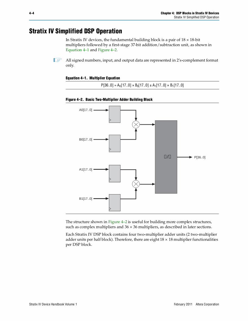
Stratix IV Simplified DSP OperationIn Stratix IV devices, the fundamental building block is a pair of 18 × 18-bit multipliers followed by a first-stage 37-bit addition/subtraction unit, as shown in Equation 4–1 and Figure 4–2.
1 All signed numbers, input, and output data are represented in 2’s-complement format only.
The structure shown in Figure 4–2 is useful for building more complex structures, such as complex multipliers and 36 × 36 multipliers, as described in later sections.
Each Stratix IV DSP block contains four two-multiplier adder units (2 two-multiplier adder units per half block). Therefore, there are eight 18 × 18 multiplier functionalities per DSP block.
Figure 4–2. Basic Two-Multiplier Adder Building Block
D Q
D Q
A0[17..0]
A1[17..0]
B1[17..0]
B0[17..0]
P[36..0]+/-
Stratix IV Device Handbook Volume 1 February 2011 Altera Corporation
Chapter 4: DSP Blocks in Stratix IV Devices 4–5Stratix IV Simplified DSP Operation
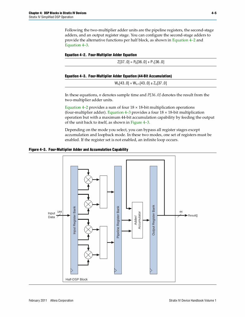
Following the two-multiplier adder units are the pipeline registers, the second-stage adders, and an output register stage. You can configure the second-stage adders to provide the alternative functions per half block, as shown in Equation 4–2 and Equation 4–3.
In these equations, n denotes sample time and P[36..0] denotes the result from the two-multiplier adder units.
Equation 4–2 provides a sum of four 18 × 18-bit multiplication operations (four-multiplier adder). Equation 4–3 provides a four 18 × 18-bit multiplication operation but with a maximum 44-bit accumulation capability by feeding the output of the unit back to itself, as shown in Figure 4–3.
Depending on the mode you select, you can bypass all register stages except accumulation and loopback mode. In these two modes, one set of registers must be enabled. If the register set is not enabled, an infinite loop occurs.
Figure 4–3. Four-Multiplier Adder and Accumulation Capability
144 44InputData
Inpu
t Reg
iste
r B
ank
Add
er/
Acc
umul
ator
Out
put R
egis
ter
Ban
k
Half-DSP Block
Result[]
Pip
elin
e R
egis
ter
Ban
k
February 2011 Altera Corporation Stratix IV Device Handbook Volume 1
4–6 Chapter 4: DSP Blocks in Stratix IV DevicesStratix IV Simplified DSP Operation
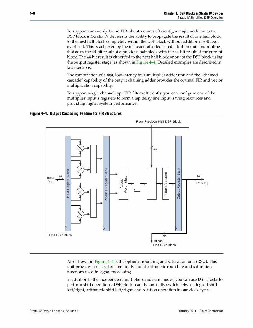
To support commonly found FIR-like structures efficiently, a major addition to the DSP block in Stratix IV devices is the ability to propagate the result of one half block to the next half block completely within the DSP block without additional soft logic overhead. This is achieved by the inclusion of a dedicated addition unit and routing that adds the 44-bit result of a previous half block with the 44-bit result of the current block. The 44-bit result is either fed to the next half block or out of the DSP block using the output register stage, as shown in Figure 4–4. Detailed examples are described in later sections.
The combination of a fast, low-latency four-multiplier adder unit and the “chained cascade” capability of the output chaining adder provides the optimal FIR and vector multiplication capability.
To support single-channel type FIR filters efficiently, you can configure one of the multiplier input’s registers to form a tap delay line input, saving resources and providing higher system performance.
Also shown in Figure 4–4 is the optional rounding and saturation unit (RSU). This unit provides a rich set of commonly found arithmetic rounding and saturation functions used in signal processing.
In addition to the independent multipliers and sum modes, you can use DSP blocks to perform shift operations. DSP blocks can dynamically switch between logical shift left/right, arithmetic shift left/right, and rotation operation in one clock cycle.
Figure 4–4. Output Cascading Feature for FIR Structures
144 44
44
From Previous Half DSP Block
To Next Half DSP Block
InputData
Inpu
t Reg
iste
r B
ank
Add
er/
Acc
umul
ator
Rou
nd/S
atur
ate
Out
put R
egis
ter
Ban
k
44Half DSP Block
Result[]
Pip
elin
e R
egis
ter
Ban
k
Stratix IV Device Handbook Volume 1 February 2011 Altera Corporation
Chapter 4: DSP Blocks in Stratix IV Devices 4–7Stratix IV Simplified DSP Operation
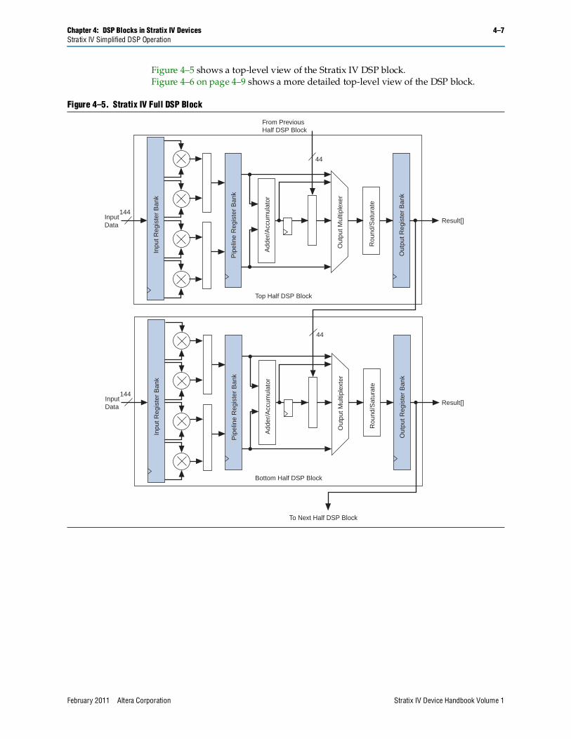
Figure 4–5 shows a top-level view of the Stratix IV DSP block. Figure 4–6 on page 4–9 shows a more detailed top-level view of the DSP block.
Figure 4–5. Stratix IV Full DSP Block
Inpu
t Reg
iste
r B
ank
Pip
elin
e R
egis
ter
Ban
k
Add
er/A
ccum
ulat
or
Out
put M
ultip
lexe
r
Rou
nd/S
atur
ate
Out
put R
egis
ter
Ban
k
From Previous Half DSP Block
To Next Half DSP Block
44
44
InputData
144
Inpu
t Reg
iste
r B
ank
Pip
elin
e R
egis
ter
Ban
k
Add
er/A
ccum
ulat
or
Out
put M
ultip
lext
er
Rou
nd/S
atur
ate
Out
put R
egis
ter
Ban
kInputData
144
Top Half DSP Block
Bottom Half DSP Block
Result[]
Result[]
February 2011 Altera Corporation Stratix IV Device Handbook Volume 1
4–8 Chapter 4: DSP Blocks in Stratix IV DevicesStratix IV Operational Modes Overview
Stratix IV Operational Modes OverviewYou can use each Stratix IV DSP block in one of five basic operational modes. Table 4–2 lists the five basic operational modes and the number of multipliers that you can implement within a single DSP block, depending on the mode.
The DSP block consists of two identical halves (the top half and bottom half). Each half has four 18 × 18 multipliers.
The Quartus® II software includes megafunctions used to control the mode of operation of the multipliers. After making the appropriate parameter settings using the megafunction’s MegaWizard™ Plug-In Manager, the Quartus II software automatically configures the DSP block.
Stratix IV DSP blocks can operate in different modes simultaneously. Each half block is fully independent except for the sharing of the three clock, ena, and aclr signals. For example, you can break down a single DSP block to operate a 9 × 9 multiplier in one half block and an 18 × 18 two-multiplier adder in the other half block. This increases DSP block resource efficiency and allows you to implement more multipliers within a Stratix IV device. The Quartus II software automatically places multipliers that can share the same DSP block resources within the same block.
Table 4–2. Stratix IV DSP Block Operation Modes
Mode Multiplier in Width
# of Mults
# per Block
Signed or Unsigned
RND, SAT
In Shift Register
Chainout Adder
1st Stage Add/Sub
2nd Stage
Add/Acc
Independent Multiplier
9 bits 1 8 Both No No No — —
12 bits 1 6 Both No No No — —
18 bits 1 4 Both Yes Yes No — —
36 bits 1 2 Both No No No — —
Double 1 2 Both No No No — —
Two-Multiplier Adder (1)
18 bits 2 4 Signed (4) Yes No No Both —
Four-Multiplier Adder
18 bits 4 2 Both Yes Yes Yes Both Add Only
Multiply Accumulate
18 bits 4 2 Both Yes Yes Yes Both Both
Shift (2) 36 bits (3) 1 2 Both No No — — —
High Precision Multiplier Adder
18× 36 2 2 Both No No No — Add Only
Notes to Table 4–2:
(1) This mode also supports loopback mode. In loopback mode, the number of loopback multipliers per DSP block is two. You can use the remaining multipliers in regular two-multiplier adder mode.
(2) Dynamic shift mode supports arithmetic shift left, arithmetic shift right, logical shift left, logical shift right, and rotation operation.(3) Dynamic shift mode operates on a 32-bit input vector but the multiplier width is configured as 36 bits.(4) Unsigned value is also supported but you must ensure that the result can be contained within 36 bits.
Stratix IV Device Handbook Volume 1 February 2011 Altera Corporation
Chapter 4: DSP Blocks in Stratix IV Devices 4–9Stratix IV DSP Block Resource Descriptions
Stratix IV DSP Block Resource DescriptionsThe DSP block consists of the following elements:
■ Input register bank
■ Four two-multiplier adders
■ Pipeline register bank
■ Two second-stage adders
■ Four rounding and saturation logic units
■ Second adder register and output register bank
Figure 4–6 shows a detailed overall architecture of the top half of the DSP block. Table 4–9 on page 4–34 shows a list of DSP block dynamic signals.
Figure 4–6. Half DSP Block Architecture
Notes to Figure 4–6:
(1) Block output for accumulator overflow and saturate overflow.(2) Block output for saturation overflow of chainout.(3) The chainin port must only be connected to chainout of the previous DSP blocks and must not be connected to general routings.
chainin[ ] (3)
scanina[ ]
dataa_0[ ]
datab_0[ ]dataa_1[ ]
datab_1[ ]
dataa_2[ ]
datab_2[ ]
dataa_3[ ]
scanouta chainout
datab_3[ ]
Inpu
t Reg
iste
r B
ank
Firs
t Sta
ge A
dder
Firs
t Sta
ge A
dder
Pip
elin
e R
egis
ter
Ban
k
Sec
ond
Sta
ge A
dder
/Acc
umul
ator
Firs
t Rou
nd/S
atur
ate
Sec
ond
Add
er R
egis
ter
Ban
k
Cha
inou
t Add
er
Sec
ond
Rou
nd/S
atur
ate
Out
put R
egis
ter
Ban
k
Shi
ft/R
otat
e
result[ ]
clock[3..0]ena[3..0]alcr[3..0]
zero_loopbackaccum_sload
zero_chainoutchainout_round
chainout_saturate
signasignb
output_roundoutput_saturate
rotateshift_right
overflow (1)
chainout_sat_overflow (2)
Half-DSP Block
loopback
Mul
tiple
xer
February 2011 Altera Corporation Stratix IV Device Handbook Volume 1
4–10 Chapter 4: DSP Blocks in Stratix IV DevicesStratix IV DSP Block Resource Descriptions
Input RegistersAll of the DSP block registers are triggered by the positive edge of the clock signal and are cleared after power up. Each multiplier operand can feed an input register or go directly to the multiplier, bypassing the input registers. The following DSP block signals control the input registers within the DSP block:
■ clock[3..0]
■ ena[3..0]
■ aclr[3..0]
Every DSP block has nine 18-bit data input register banks per half DSP block. Every half DSP block has the option to use the eight data register banks as inputs to the four multipliers. The special ninth register bank is a delay register required by modes that use both the cascade and chainout features of the DSP block. Use the ninth register bank to balance the latency requirements when using the chained cascade feature.
Stratix IV Device Handbook Volume 1 February 2011 Altera Corporation
Chapter 4: DSP Blocks in Stratix IV Devices 4–11Stratix IV DSP Block Resource Descriptions
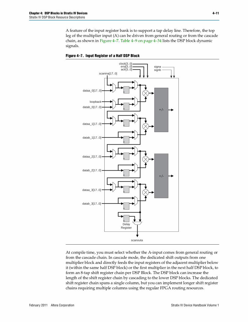
A feature of the input register bank is to support a tap delay line. Therefore, the top leg of the multiplier input (A) can be driven from general routing or from the cascade chain, as shown in Figure 4–7. Table 4–9 on page 4–34 lists the DSP block dynamic signals.
At compile time, you must select whether the A-input comes from general routing or from the cascade chain. In cascade mode, the dedicated shift outputs from one multiplier block and directly feeds the input registers of the adjacent multiplier below it (within the same half DSP block) or the first multiplier in the next half DSP block, to form an 8-tap shift register chain per DSP Block. The DSP block can increase the length of the shift register chain by cascading to the lower DSP blocks. The dedicated shift register chain spans a single column, but you can implement longer shift register chains requiring multiple columns using the regular FPGA routing resources.
Figure 4–7. Input Register of a Half DSP Block
+/-
+/-
signasignb
clock[3..0]ena[3..0]aclr[3..0]
scanina[17..0]
dataa_0[17..0]
loopback
datab_0[17..0]
dataa_1[17..0]
datab_1[17..0]
dataa_2[17..0]
datab_2[17..0]
dataa_3[17..0]
datab_3[17..0]
scanouta
DelayRegister
February 2011 Altera Corporation Stratix IV Device Handbook Volume 1
4–12 Chapter 4: DSP Blocks in Stratix IV DevicesStratix IV DSP Block Resource Descriptions
Shift registers are useful in DSP functions such as FIR filters. When implementing 18 × 18 or smaller width multipliers, you do not need external logic to create the shift register chain because the input shift registers are internal to the DSP block. This implementation significantly reduces the logical element (LE) resources required, avoids routing congestion, and results in predictable timing.
The first multiplier in every half DSP block (top- and bottom-half) in Stratix IV devices has a multiplexer for the first multiplier B-input (lower-leg input) register to select between general routing and loopback, as shown in Figure 4–6 on page 4–9. In loopback mode, the most significant 18-bit registered outputs are connected as feedback to the multiplier input of the first top multiplier in each half DSP block. Loopback modes are used by recursive filters where the previous output is needed to compute the current output.
Loopback mode is described in “Two-Multiplier Adder Sum Mode” on page 4–22.
Table 4–3 lists input register modes for the DSP block.
Multiplier and First-Stage AdderThe multiplier stage natively supports 9 × 9, 12 × 12, 18 × 18, or 36 × 36 multipliers. Other wordlengths are padded up to the nearest appropriate native wordlength; for example, 16 × 16 would be padded up to use 18 × 18. For more information, refer to “Independent Multiplier Modes” on page 4–15. Depending on the data width of the multiplier, a single DSP block can perform many multiplications in parallel.
Each multiplier operand can be a unique signed or unsigned number. Two dynamic signals, signa and signb, control the representation of each operand, respectively. A logic 1 value on the signa/signb signal indicates that data A/data B is a signed number; a logic 0 value indicates an unsigned number. Table 4–4 lists the sign of the multiplication result for the various operand sign representations. The result of the multiplication is signed if any one of the operands is a signed value.
(1) Multiplier operand input wordlengths are statically configured at compile time.(2) Available only on the A-operand.(3) Only one loopback input is allowed per half block. For more information, refer to Figure 4–15 on page 4–24.
Table 4–4. Multiplier Sign Representation
Data A (signa Value) Data B (signb Value) Result
Unsigned (logic 0) Unsigned (logic 0) Unsigned
Unsigned (logic 0) Signed (logic 1) Signed
Signed (logic 1) Unsigned (logic 0) Signed
Signed (logic 1) Signed (logic 1) Signed
Stratix IV Device Handbook Volume 1 February 2011 Altera Corporation
Chapter 4: DSP Blocks in Stratix IV Devices 4–13Stratix IV DSP Block Resource Descriptions
Each half block has its own signa and signb signal. Therefore, all of the data A inputs feeding the same half DSP block must have the same sign representation. Similarly, all of the data B inputs feeding the same half DSP block must have the same sign representation. The multiplier offers full precision regardless of the sign representation in all operational modes except for full precision 18 × 18 loopback and two-multiplier adder modes. For more information, refer to “Two-Multiplier Adder Sum Mode” on page 4–22.
1 By default, when the signa and signb signals are unused, the Quartus II software sets the multiplier to perform unsigned multiplication.
Figure 4–6 on page 4–9 shows that the outputs of the multipliers are the only outputs that can feed into the first-stage adder. There are four first-stage adders in a DSP block (two adders per half DSP block). The first-stage adder block has the ability to perform addition and subtraction. The control signal for addition or subtraction is static and has to be configured after compile time. The first-stage adders are used by the sum modes to compute the sum of two multipliers, 18 × 18-complex multipliers, and to perform the first stage of a 36 × 36 multiply and shift operations.
Depending on your specifications, the output of the first-stage adder has the option to feed into the pipeline registers, second-stage adder, rounding and saturation unit, or output registers.
Pipeline Register StageFigure 4–6 on page 4–9 shows that the output from the first-stage adder can either feed or bypass the pipeline registers. Pipeline registers increase the DSP block’s maximum performance (at the expense of extra cycles of latency), especially when using the subsequent DSP block stages. Pipeline registers split up the long signal path between the input registers/multiplier/first-stage adder and the second-stage adder/round-and-saturation/output registers, creating two shorter paths.
Second-Stage AdderThere are four individual 44-bit second-stage adders per DSP block (two adders per half DSP block). You can configure the second-stage adders as follows:
■ The final stage of a 36-bit multiplier
■ A sum of four (18 × 18)
■ An accumulator (44-bits maximum)
■ A chained output summation (44-bits maximum)
1 You can use the chained-output adder at the same time as a second-level adder in chained output summation mode.
The output of the second-stage adder has the option to go into the rounding and saturation logic unit or the output register.
1 You cannot use the second-stage adder independently from the multiplier and first-stage adder.
February 2011 Altera Corporation Stratix IV Device Handbook Volume 1
4–14 Chapter 4: DSP Blocks in Stratix IV DevicesStratix IV DSP Block Resource Descriptions
Rounding and Saturation StageThe rounding and saturation logic units are located at the output of the 44-bit second-stage adder (the rounding logic unit followed by the saturation logic unit). There are two rounding and saturation logic units per half DSP block. The input to the rounding and saturation logic unit can come from one of the following stages:
■ Output of the multiplier (independent multiply mode in 18 × 18)
■ Output of the first-stage adder (two-multiplier adder)
■ Output of the pipeline registers
■ Output of the second-stage adder (four-multiplier adder and multiply-accumulate mode in 18 × 18)
These stages are described in “Stratix IV Operational Mode Descriptions” on page 4–15.
The rounding and saturation logic unit is controlled by the dynamic rounding and saturate signals, respectively. A logic 1 value on the rounding and/or saturate signals enables the rounding and/or saturate logic unit, respectively.
1 You can use the rounding and saturation logic units together or independently.
Second Adder and Output RegistersThe second adder register and output register banks are two banks of 44-bit registers that you can combine to form larger 72-bit banks to support 36 × 36 output results.
The outputs of the different stages in the Stratix IV devices are routed to the output registers through an output selection unit. Depending on the operational mode of the DSP block, the output selection unit selects whether the outputs of the DSP blocks comes from the outputs of the multiplier block, first-stage adder, pipeline registers, second-stage adder, or the rounding and saturation logic unit. The output selection unit is set automatically by the software, based on the DSP block operational mode you specified, and has the option to either drive or bypass the output registers. The exception is when you use the block in shift mode, in which case you dynamically control the output-select multiplexer directly.
When the DSP block is configured in chained cascaded output mode, both of the second-stage adders are used. Use the first one for performing a four-multiplier adder; use the second for the chainout adder.
The outputs of the four-multiplier adder are routed to the second-stage adder registers before they enter the chainout adder. The output of the chainout adder goes to the regular output register bank. Depending on the configuration, you can route the chainout results to the input of the next half block’s chainout adder input or to the general fabric (functioning as regular output registers). For more information, refer to “Stratix IV Operational Mode Descriptions” on page 4–15.
Stratix IV Device Handbook Volume 1 February 2011 Altera Corporation
Chapter 4: DSP Blocks in Stratix IV Devices 4–15Stratix IV Operational Mode Descriptions
The second-stage and output registers are triggered by the positive edge of the clock signal and are cleared after power up. The following DSP block signals control the output registers within the DSP block:
■ clock[3..0]
■ ena[3..0]
■ aclr[3..0]
Stratix IV Operational Mode DescriptionsThis section contains an explanation of different operational modes in Stratix IV devices.
Independent Multiplier ModesIn independent input and output multiplier mode, the DSP block performs individual multiplication operations for general-purpose multipliers.
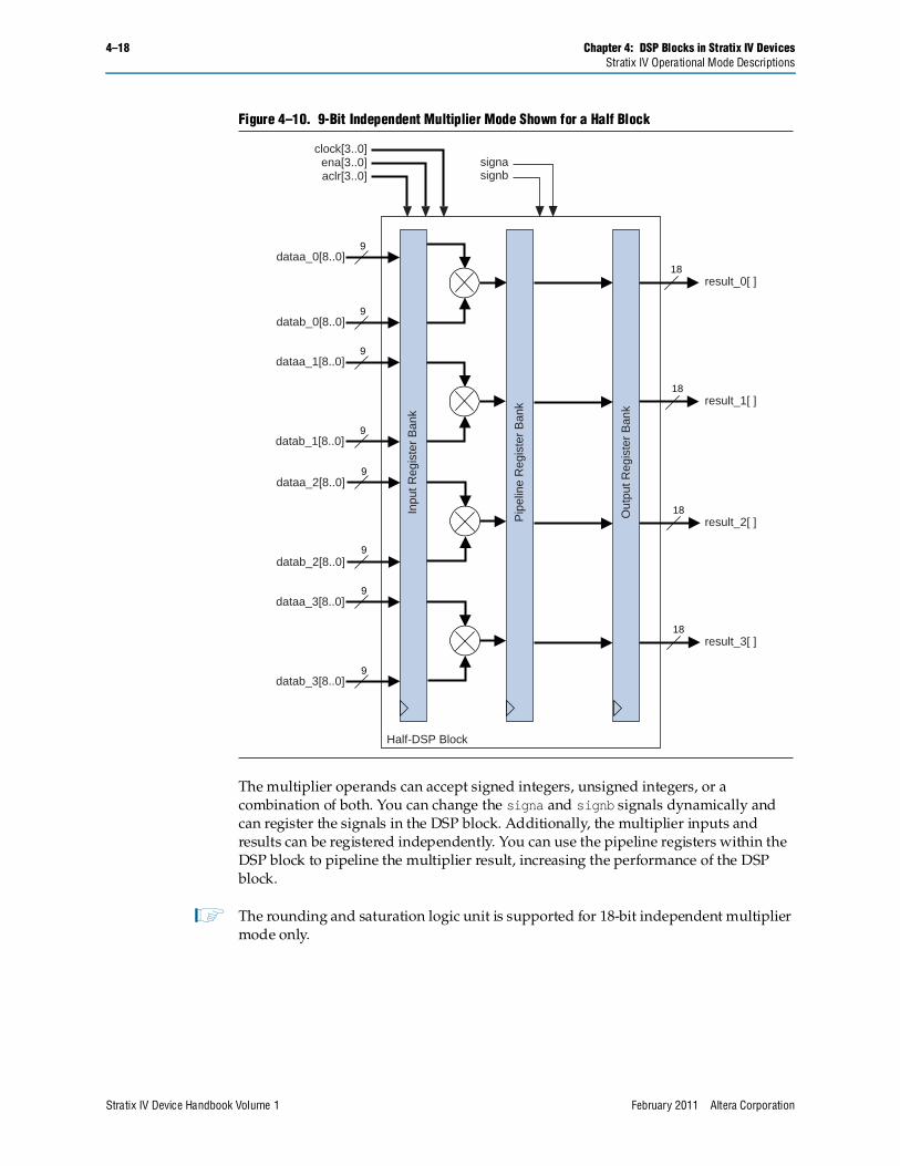
9-, 12-, and 18-Bit MultiplierYou can configure each DSP block multiplier for 9-, 12-, or 18-bit multiplication. A single DSP block can support up to eight individual 9 × 9 multipliers, six individual 12 × 12 multipliers, or four individual 18 × 18 multipliers. For operand widths up to 9 bits, a 9 × 9 multiplier is implemented. For operand widths from 10 to 12 bits, a 12 × 12 multiplier is implemented, and for operand widths from 13 to 18 bits, an 18 × 18 multiplier is implemented. This is done by the Quartus II software by zero-padding the LSBs. Figure 4–8, Figure 4–9, and Figure 4–10 show the DSP block in the independent multiplier operation. Table 4–9 on page 4–34 lists the dynamic signals for the DSP block.
February 2011 Altera Corporation Stratix IV Device Handbook Volume 1
4–16 Chapter 4: DSP Blocks in Stratix IV DevicesStratix IV Operational Mode Descriptions
Figure 4–8. 18-Bit Independent Multiplier Mode Shown for a Half DSP Block
Note to Figure 4–8:(1) Block output for accumulator overflow and saturate overflow.
clock[3..0]
ena[3..0]
aclr[3..0]
signa
signb
output_round
output_saturate
overflow (1)
36
36
dataa_0[17..0]
datab_0[17..0]
dataa_1[17..0]
datab_1[17..0]
Half-DSP Block
Inpu
t Reg
iste
r B
ank
Pip
elin
e R
egis
ter
Ban
k
Rou
nd/S
atur
ate
Rou
nd/S
atur
ate
Out
put R
egis
ter
Ban
k
18
18
18
18
result_0[ ]
result_1[ ]
Stratix IV Device Handbook Volume 1 February 2011 Altera Corporation
Chapter 4: DSP Blocks in Stratix IV Devices 4–17Stratix IV Operational Mode Descriptions
Figure 4–9. 12-Bit Independent Multiplier Mode Shown for a Half DSP Block
24
12
12
12
12
12
12
24
24
Inpu
t Reg
iste
r B
ank
Pip
elin
e R
egis
ter
Ban
k
Out
put R
egis
ter
Ban
k
clock[3..0]ena[3..0]aclr[3..0]
signasignb
Half-DSP Block
dataa_0[11..0]
datab_0[11..0]
dataa_1[11..0]
datab_1[11..0]
dataa_2[11..0]
datab_2[11..0]
result_0[ ]
result_1[ ]
result_2[ ]
February 2011 Altera Corporation Stratix IV Device Handbook Volume 1
4–18 Chapter 4: DSP Blocks in Stratix IV DevicesStratix IV Operational Mode Descriptions
The multiplier operands can accept signed integers, unsigned integers, or a combination of both. You can change the signa and signb signals dynamically and can register the signals in the DSP block. Additionally, the multiplier inputs and results can be registered independently. You can use the pipeline registers within the DSP block to pipeline the multiplier result, increasing the performance of the DSP block.
1 The rounding and saturation logic unit is supported for 18-bit independent multiplier mode only.
Figure 4–10. 9-Bit Independent Multiplier Mode Shown for a Half Block
18
9
9
9
9
18
9
9
18
9
9
18
Inpu
t Reg
iste
r B
ank
Pip
elin
e R
egis
ter
Ban
k
Out
put R
egis
ter
Ban
k
dataa_0[8..0]
datab_0[8..0]
dataa_1[8..0]
datab_1[8..0]
dataa_2[8..0]
datab_2[8..0]
dataa_3[8..0]
datab_3[8..0]
Half-DSP Block
clock[3..0]ena[3..0]aclr[3..0]
signasignb
result_0[ ]
result_1[ ]
result_2[ ]
result_3[ ]
Stratix IV Device Handbook Volume 1 February 2011 Altera Corporation
Chapter 4: DSP Blocks in Stratix IV Devices 4–19Stratix IV Operational Mode Descriptions
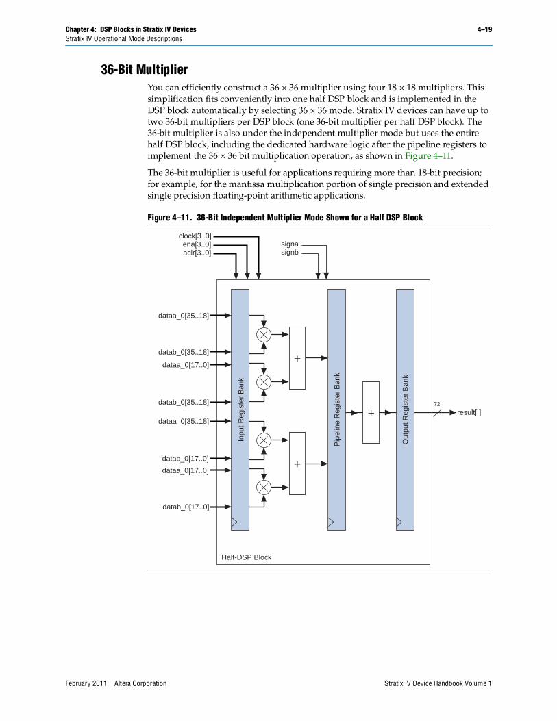
36-Bit MultiplierYou can efficiently construct a 36 × 36 multiplier using four 18 × 18 multipliers. This simplification fits conveniently into one half DSP block and is implemented in the DSP block automatically by selecting 36 × 36 mode. Stratix IV devices can have up to two 36-bit multipliers per DSP block (one 36-bit multiplier per half DSP block). The 36-bit multiplier is also under the independent multiplier mode but uses the entire half DSP block, including the dedicated hardware logic after the pipeline registers to implement the 36 × 36 bit multiplication operation, as shown in Figure 4–11.
The 36-bit multiplier is useful for applications requiring more than 18-bit precision; for example, for the mantissa multiplication portion of single precision and extended single precision floating-point arithmetic applications.
Figure 4–11. 36-Bit Independent Multiplier Mode Shown for a Half DSP Block
Pip
elin
e R
egis
ter
Ban
k
Inpu
t Reg
iste
r B
ank
Out
put R
egis
ter
Ban
k
Half-DSP Block
dataa_0[35..18]
datab_0[35..18]
dataa_0[17..0]
datab_0[35..18]
dataa_0[35..18]
datab_0[17..0]
dataa_0[17..0]
datab_0[17..0]
72
clock[3..0]ena[3..0]aclr[3..0]
signasignb
+
+
+ result[ ]
February 2011 Altera Corporation Stratix IV Device Handbook Volume 1
4–20 Chapter 4: DSP Blocks in Stratix IV DevicesStratix IV Operational Mode Descriptions
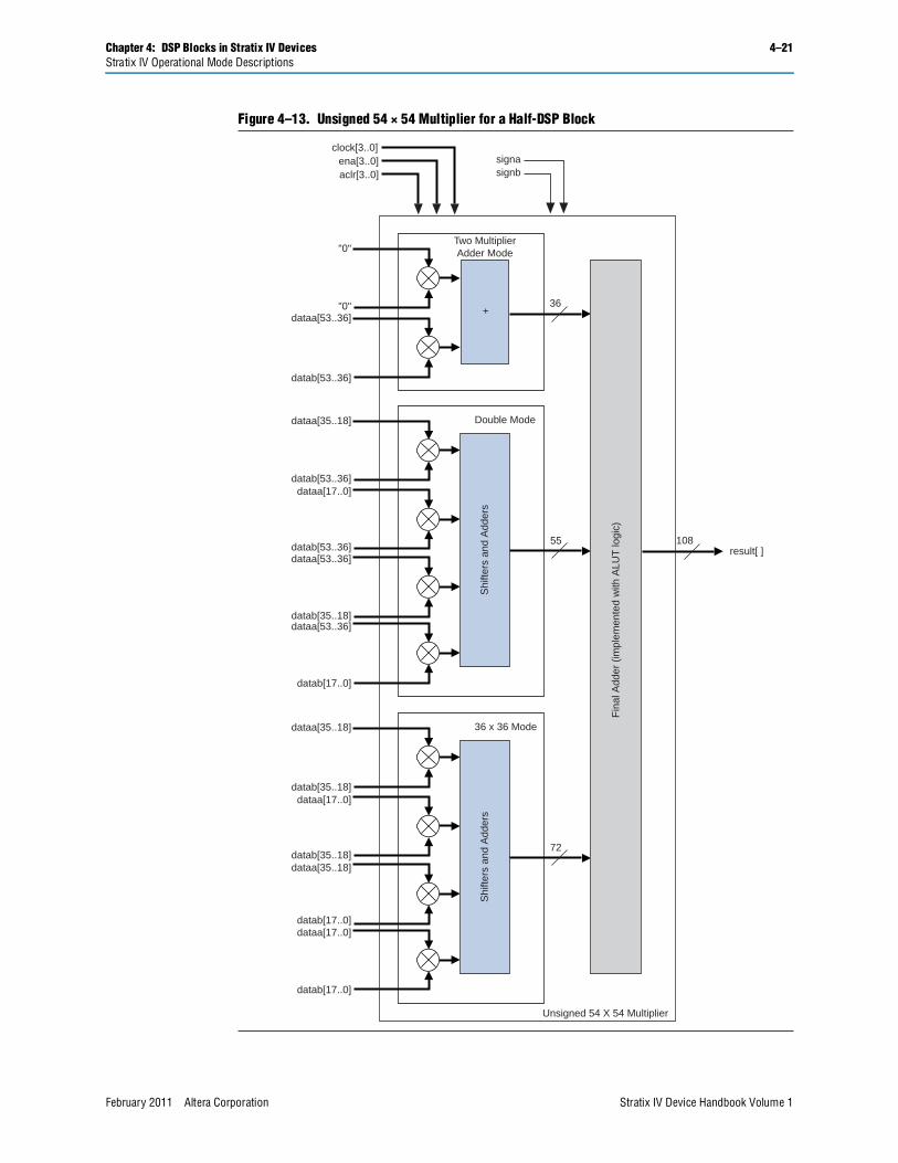
Double MultiplierYou can configure the Stratix IV DSP block to efficiently support a signed or unsigned 54 × 54-bit multiplier that is required to compute the mantissa portion of an IEEE double-precision floating point multiplication. You can build a 54 × 54-bit multiplier using basic 18 × 18 multipliers, shifters, and adders. In order to efficiently use the Stratix IV DSP block’s built-in shifters and adders, a special double mode (partial 54 × 54 multiplier) is available that is a slight modification to the basic 36 × 36 multiplier mode, as shown in Figure 4–12 and Figure 4–13.
Figure 4–12. Double Mode Shown for a Half DSP Block
Pip
elin
e R
egis
ter
Ban
k
Inpu
t Reg
iste
r B
ank
Out
put R
egis
ter
Ban
k
Half-DSP Block
dataa_0[35..18]
datab_0[35..18]
dataa_0[17..0]
datab_0[35..18]
dataa_0[35..18]
datab_0[17..0]
dataa_0[17..0]
datab_0[17..0]
72
clock[3..0]ena[3..0]aclr[3..0]
signasignb
+
+
+ result[ ]
Stratix IV Device Handbook Volume 1 February 2011 Altera Corporation
Chapter 4: DSP Blocks in Stratix IV Devices 4–21Stratix IV Operational Mode Descriptions
Figure 4–13. Unsigned 54 × 54 Multiplier for a Half-DSP Block
Shi
fters
and
Add
ers
Double Mode
Shi
fters
and
Add
ers
36 x 36 Mode
+
Two MultiplierAdder Mode
Fin
al A
dder
(im
plem
ente
d w
ith A
LUT
logi
c)
36
55
72
108result[ ]
Unsigned 54 X 54 Multiplier
"0"
"0"dataa[53..36]
dataa[53..36]
dataa[53..36]
datab[53..36]
dataa[35..18]
datab[53..36]dataa[17..0]
datab[53..36]
datab[35..18]
datab[17..0]
clock[3..0]ena[3..0]aclr[3..0]
signasignb
dataa[35..18]
dataa[35..18]datab[35..18]
datab[17..0]
datab[17..0]
dataa[17..0]
datab[35..18]dataa[17..0]
February 2011 Altera Corporation Stratix IV Device Handbook Volume 1
4–22 Chapter 4: DSP Blocks in Stratix IV DevicesStratix IV Operational Mode Descriptions
Two-Multiplier Adder Sum ModeIn a two-multiplier adder configuration, the DSP block can implement four 18-bit two-multiplier adders (2 two-multiplier adders per half DSP block). You can configure the adders to take the sum or difference of two multiplier outputs. You must select summation or subtraction at compile time. The two-multiplier adder function is useful for applications such as FFTs, complex FIR, and IIR filters. Figure 4–14 on page 4–23 shows the DSP block configured in two-multiplier adder mode.
Loopback mode is the other sub-feature of the two-multiplier adder mode. Figure 4–15 on page 4–24 shows the DSP block configured in the loopback mode. This mode takes the 36-bit summation result of the two multipliers and feeds back the most significant 18-bits to the input. The lower 18-bits are discarded. You have the option to disable or zero-out the loopback data by using the dynamic zero_loopback signal. A logic 1 value on the zero_loopback signal selects the zeroed data or disables the looped back data, while a logic 0 selects the looped back data.
1 You must select the option to use loopback mode or the general two-multiplier adder mode at compile time.
For two-multiplier adder mode, if all the inputs are full 18-bit and unsigned, the result requires 37 bits. As the output data width in two-multiplier adder mode is limited to 36 bits, this 37-bit output requirement is not allowed. Any other combination that does not violate the 36-bit maximum result is permitted; for example, two 16 × 16 signed two-multiplier adders is valid.
Two-multiplier adder mode supports the rounding and saturation logic unit. You can use the pipeline registers and output registers within the DSP block to pipeline the multiplier-adder result, increasing the performance of the DSP block.
Stratix IV Device Handbook Volume 1 February 2011 Altera Corporation
Chapter 4: DSP Blocks in Stratix IV Devices 4–23Stratix IV Operational Mode Descriptions
Figure 4–14. Two-Multiplier Adder Mode Shown for a Half DSP Block
Note to Figure 4–14:(1) Block output for accumulator overflow and saturate overflow.
Inpu
t Reg
iste
r B
ank
Pip
elin
e R
egis
ter
Ban
k
Rou
nd/S
atur
ate
Out
put R
egis
ter
Ban
k
clock[3..0]
ena[3..0]
aclr[3..0]
signa
signb
output_round
output_saturate
overflow (1)
result[ ]+
dataa_0[17..0]
datab_0[17..0]
dataa_1[17..0]
datab_1[17..0]
Half-DSP Block
February 2011 Altera Corporation Stratix IV Device Handbook Volume 1
4–24 Chapter 4: DSP Blocks in Stratix IV DevicesStratix IV Operational Mode Descriptions
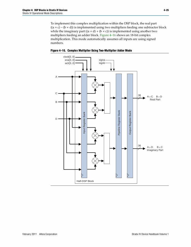
18 x 18 Complex MultiplyYou can configure the DSP block to implement complex multipliers using two-multiplier adder mode. A single half DSP block can implement one 18-bit complex multiplier.
Equation 4–4 shows a complex multiplication.
Figure 4–15. Loopback Mode for a Half DSP Block
Note to Figure 4–15:
(1) Block output for accumulator overflow and saturate overflow.
Stratix IV Device Handbook Volume 1 February 2011 Altera Corporation
Chapter 4: DSP Blocks in Stratix IV Devices 4–25Stratix IV Operational Mode Descriptions
To implement this complex multiplication within the DSP block, the real part ((a × c) – (b × d)) is implemented using two multipliers feeding one subtractor block while the imaginary part ((a × d) + (b × c)) is implemented using another two multipliers feeding an adder block. Figure 4–16 shows an 18-bit complex multiplication. This mode automatically assumes all inputs are using signed numbers.
Figure 4–16. Complex Multiplier Using Two-Multiplier Adder Mode
Inpu
t Reg
iste
r B
ank
Pip
elin
e R
egis
ter
Ban
k
Out
put R
egis
ter
Ban
k
A x C B x DReal Part
A x D B x CImaginary Part
clock[3..0]ena[3..0]aclr[3..0]
signasignb
A
C
B
D
Half-DSP Block
36
36
February 2011 Altera Corporation Stratix IV Device Handbook Volume 1
4–26 Chapter 4: DSP Blocks in Stratix IV DevicesStratix IV Operational Mode Descriptions
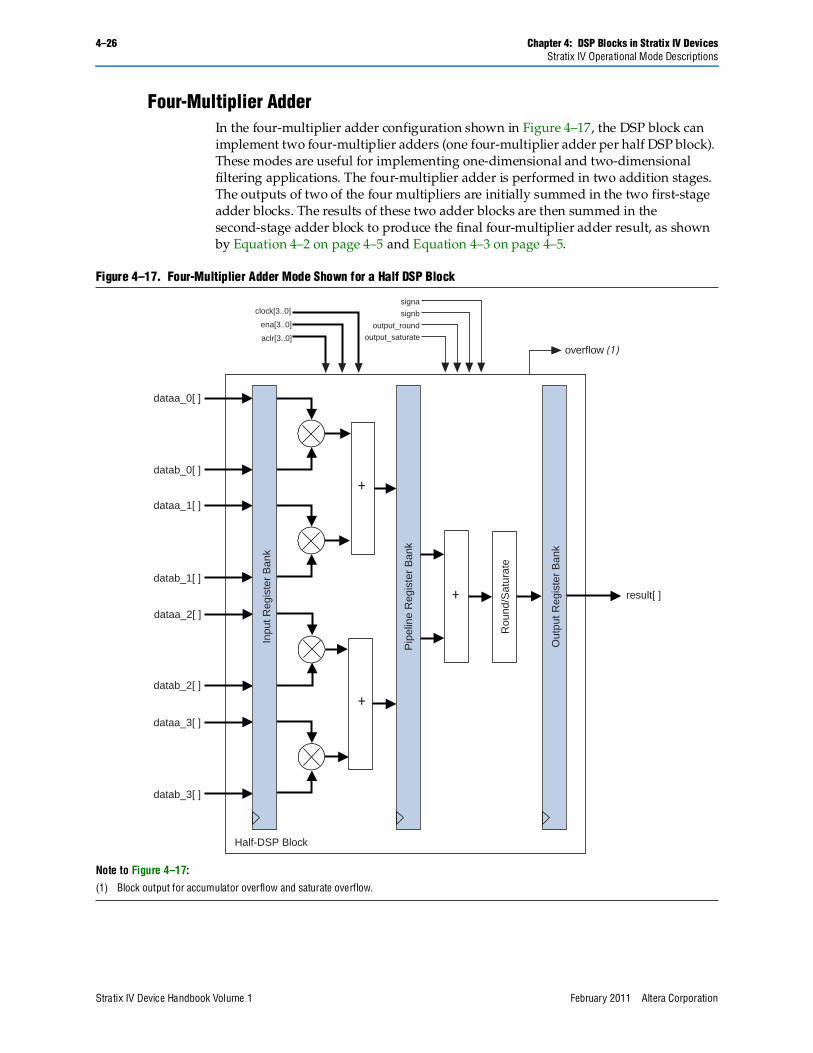
Four-Multiplier AdderIn the four-multiplier adder configuration shown in Figure 4–17, the DSP block can implement two four-multiplier adders (one four-multiplier adder per half DSP block). These modes are useful for implementing one-dimensional and two-dimensional filtering applications. The four-multiplier adder is performed in two addition stages. The outputs of two of the four multipliers are initially summed in the two first-stage adder blocks. The results of these two adder blocks are then summed in the second-stage adder block to produce the final four-multiplier adder result, as shown by Equation 4–2 on page 4–5 and Equation 4–3 on page 4–5.
Figure 4–17. Four-Multiplier Adder Mode Shown for a Half DSP Block
Note to Figure 4–17:(1) Block output for accumulator overflow and saturate overflow.
clock[3..0]
ena[3..0]
aclr[3..0]
signa
signb
output_round
output_saturate
overflow (1)
Inpu
t Reg
iste
r B
ank
Pip
elin
e R
egis
ter
Ban
k
Rou
nd/S
atur
ate
Out
put R
egis
ter
Ban
k
dataa_0[ ]
datab_0[ ]
dataa_1[ ]
datab_1[ ]
dataa_2[ ]
datab_2[ ]
dataa_3[ ]
datab_3[ ]
Half-DSP Block
+
+
+
result[ ]
Stratix IV Device Handbook Volume 1 February 2011 Altera Corporation
Chapter 4: DSP Blocks in Stratix IV Devices 4–27Stratix IV Operational Mode Descriptions
Four-multiplier adder mode supports the rounding and saturation logic unit. You can use the pipeline registers and output registers within the DSP block to pipeline the multiplier-adder result, increasing the performance of the DSP block.
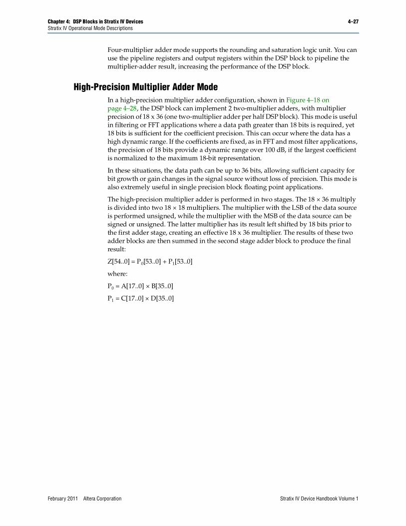
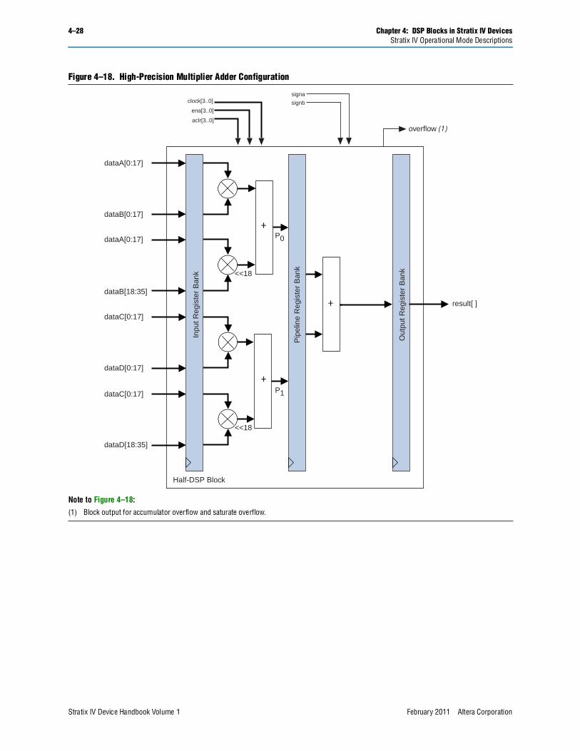
High-Precision Multiplier Adder ModeIn a high-precision multiplier adder configuration, shown in Figure 4–18 on page 4–28, the DSP block can implement 2 two-multiplier adders, with multiplier precision of 18 x 36 (one two-multiplier adder per half DSP block). This mode is useful in filtering or FFT applications where a data path greater than 18 bits is required, yet 18 bits is sufficient for the coefficient precision. This can occur where the data has a high dynamic range. If the coefficients are fixed, as in FFT and most filter applications, the precision of 18 bits provide a dynamic range over 100 dB, if the largest coefficient is normalized to the maximum 18-bit representation.
In these situations, the data path can be up to 36 bits, allowing sufficient capacity for bit growth or gain changes in the signal source without loss of precision. This mode is also extremely useful in single precision block floating point applications.
The high-precision multiplier adder is performed in two stages. The 18 × 36 multiply is divided into two 18 × 18 multipliers. The multiplier with the LSB of the data source is performed unsigned, while the multiplier with the MSB of the data source can be signed or unsigned. The latter multiplier has its result left shifted by 18 bits prior to the first adder stage, creating an effective 18 x 36 multiplier. The results of these two adder blocks are then summed in the second stage adder block to produce the final result:
Z[54..0] = P0[53..0] + P1[53..0]
where:
P0 = A[17..0] × B[35..0]
P1 = C[17..0] × D[35..0]
February 2011 Altera Corporation Stratix IV Device Handbook Volume 1
4–28 Chapter 4: DSP Blocks in Stratix IV DevicesStratix IV Operational Mode Descriptions
Note to Figure 4–18:(1) Block output for accumulator overflow and saturate overflow.
clock[3..0]
ena[3..0]
aclr[3..0]
signa
signb
overflow (1)
Inpu
t Reg
iste
r B
ank
Pip
elin
e R
egis
ter
Ban
k
Out
put R
egis
ter
Ban
k
dataA[0:17]
P0
P1
dataA[0:17]
dataC[0:17]
dataC[0:17]
dataD[0:17]
dataD[18:35]
dataB[0:17]
<<18
<<18
dataB[18:35]
Half-DSP Block
+
+
+
result[ ]
Stratix IV Device Handbook Volume 1 February 2011 Altera Corporation
Chapter 4: DSP Blocks in Stratix IV Devices 4–29Stratix IV Operational Mode Descriptions
Multiply Accumulate ModeIn multiply accumulate mode, the second-stage adder is configured as a 44-bit accumulator or subtractor. The output of the DSP block is looped back to the second-stage adder and added or subtracted with the two outputs of the first-stage adder block according to Equation 4–3 on page 4–5. Figure 4–19 shows the DSP block configured to operate in multiply accumulate mode.
A single DSP block can implement up to two independent 44-bit accumulators.
Figure 4–19. Multiply Accumulate Mode Shown for a Half DSP Block
Note to Figure 4–19:
(1) Block output for saturation overflow of chainout.
clock[3..0]
ena[3..0]
aclr[3..0]
signasignb
output_roundoutput_saturate
chainout_sat_overflow (1)
Inpu
t Reg
iste
r B
ank
Pip
elin
e R
egis
ter
Ban
k
Rou
nd/S
atur
ate
Out
put R
egis
ter
Ban
k
dataa_0[ ]
datab_0[ ]
dataa_1[ ]
datab_1[ ]
dataa_2[ ]
datab_2[ ]
dataa_3[ ]
datab_3[ ]
Half-DSP Block
+
+
+
result[ ]
accum_sload
44
Sec
ond
Reg
iste
r B
ank
February 2011 Altera Corporation Stratix IV Device Handbook Volume 1
4–30 Chapter 4: DSP Blocks in Stratix IV DevicesStratix IV Operational Mode Descriptions
Use the dynamic accum_sload control signal to clear the accumulation. A logic 1 value on the accum_sload signal synchronously loads the accumulator with the multiplier result only, while a logic 0 enables accumulation by adding or subtracting the output of the DSP block (accumulator feedback) to the output of the multiplier and first-stage adder.
1 You must configure the control signal for the accumulator and subtractor if static at compile time.
This mode supports the rounding and saturation logic unit because it is configured as an 18-bit multiplier accumulator. You can use the pipeline registers and output registers within the DSP block to increase the performance of the DSP block.
Shift ModesStratix IV devices support the following shift modes for 32-bit input only:
■ Arithmetic shift left, ASL[N]
■ Arithmetic shift right, ASR[32-N]
■ Logical shift left, LSL[N]
■ Logical shift right, LSR[32-N]
■ 32-bit rotator or barrel shifter, ROT[N]
1 You can switch between these modes using the dynamic rotate and shift control signals.
You can use shift mode in a Stratix IV device by using a soft embedded processor such as Nios® II to perform the dynamic shift and rotate operation. Figure 4–20 on page 4–31 shows the shift mode configuration.
Shift mode makes use of the available multipliers to logically or arithmetically shift left, right, or rotate the desired 32-bit data. You can configure the DSP block similar to the independent 36-bit multiplier mode to perform shift mode operations.
Arithmetic shift right requires a signed input vector. During an arithmetic shift right, the sign is extended to fill the MSB of the 32-bit vector. The logical shift right uses an unsigned input vector. During a logical shift right, zeros are padded in the MSBs, shifting the 32-bit vector to the right. The barrel shifter uses unsigned input vector and implements a rotation function on a 32-bit word length.
Two control signals, rotate and shift_right, together with the signa and signb signals, determine the shifting operation. Table 4–5 on page 4–31 lists examples of shift operations.
Stratix IV Device Handbook Volume 1 February 2011 Altera Corporation
Chapter 4: DSP Blocks in Stratix IV Devices 4–31Stratix IV Operational Mode Descriptions
Figure 4–20. Shift Operation Mode Shown for a Half DSP Block
clock[3..0]ena[3..0]aclr[3..0]
signasignbrotate
shift_right
Inpu
t Reg
iste
r B
ank
Pip
elin
e R
egis
ter
Ban
k
Out
put R
egis
ter
Ban
k
dataa_0[35..18]
datab_0[35..18]
dataa_0[17..0]
datab_0[35..18]
dataa_0[35..18]
datab_0[17..0]
dataa_0[17..0]
datab_0[17..0]
Half-DSP Block
+
+
+
result[ ]32
Shi
ft/R
otat
e
Table 4–5. Examples of Shift Operations
Example Signa Signb Shift Rotate A-input B-input Result
February 2011 Altera Corporation Stratix IV Device Handbook Volume 1
4–32 Chapter 4: DSP Blocks in Stratix IV DevicesStratix IV Operational Mode Descriptions
Rounding and Saturation ModeRounding and saturation functions are often required in DSP arithmetic. Use rounding to limit bit growth and its side effects; use saturation to reduce overflow and underflow side effects.
Two rounding modes are supported in Stratix IV devices:
■ Round-to-nearest-integer mode
■ Round-to-nearest-even mode
1 You must select one of these two options at compile time.
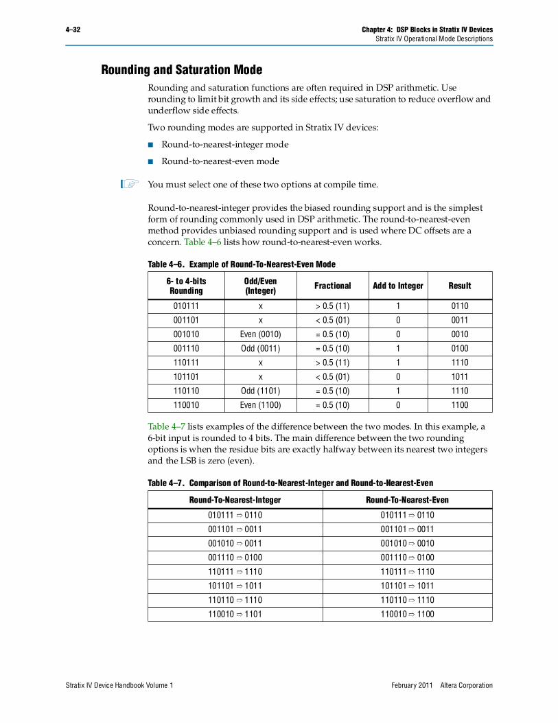
Round-to-nearest-integer provides the biased rounding support and is the simplest form of rounding commonly used in DSP arithmetic. The round-to-nearest-even method provides unbiased rounding support and is used where DC offsets are a concern. Table 4–6 lists how round-to-nearest-even works.
Table 4–7 lists examples of the difference between the two modes. In this example, a 6-bit input is rounded to 4 bits. The main difference between the two rounding options is when the residue bits are exactly halfway between its nearest two integers and the LSB is zero (even).
Table 4–6. Example of Round-To-Nearest-Even Mode
6- to 4-bits Rounding
Odd/Even (Integer) Fractional Add to Integer Result
010111 x > 0.5 (11) 1 0110
001101 x < 0.5 (01) 0 0011
001010 Even (0010) = 0.5 (10) 0 0010
001110 Odd (0011) = 0.5 (10) 1 0100
110111 x > 0.5 (11) 1 1110
101101 x < 0.5 (01) 0 1011
110110 Odd (1101) = 0.5 (10) 1 1110
110010 Even (1100) = 0.5 (10) 0 1100
Table 4–7. Comparison of Round-to-Nearest-Integer and Round-to-Nearest-Even
Round-To-Nearest-Integer Round-To-Nearest-Even
010111 ➱ 0110 010111 ➱ 0110
001101 ➱ 0011 001101 ➱ 0011
001010 ➱ 0011 001010 ➱ 0010
001110 ➱ 0100 001110 ➱ 0100
110111 ➱ 1110 110111 ➱ 1110
101101 ➱ 1011 101101 ➱ 1011
110110 ➱ 1110 110110 ➱ 1110
110010 ➱ 1101 110010 ➱ 1100
Stratix IV Device Handbook Volume 1 February 2011 Altera Corporation
Chapter 4: DSP Blocks in Stratix IV Devices 4–33Stratix IV Operational Mode Descriptions
Two saturation modes are supported in Stratix IV:
■ Asymmetric saturation mode
■ Symmetric saturation mode
1 You must select one of the two options at compile time.
In 2’s-complement format, the maximum negative number that can be represented is –2(n–1), while the maximum positive number is 2(n–1) – 1. Symmetrical saturation limits the maximum negative number to –2(n–1) + 1. For example, for 32 bits:
■ Asymmetric 32-bit saturation: Max = 0x7FFFFFFF, Min = 0x80000000
■ Symmetric 32-bit saturation: Max = 0x7FFFFFFF, Min = 0x80000001
Table 4–8 lists how saturation works. In this example, a 44-bit input is saturated to 36-bits.
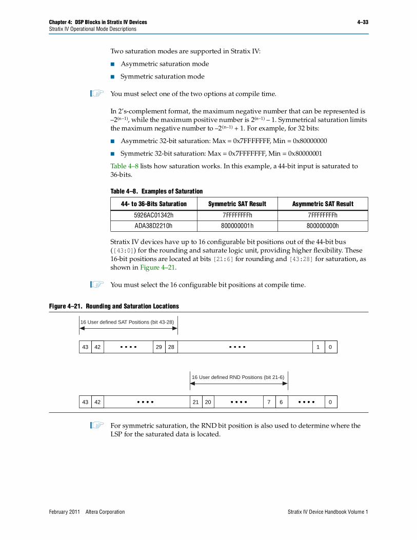
Stratix IV devices have up to 16 configurable bit positions out of the 44-bit bus ([43:0]) for the rounding and saturate logic unit, providing higher flexibility. These 16-bit positions are located at bits [21:6] for rounding and [43:28] for saturation, as shown in Figure 4–21.
1 You must select the 16 configurable bit positions at compile time.
1 For symmetric saturation, the RND bit position is also used to determine where the LSP for the saturated data is located.
Table 4–8. Examples of Saturation
44- to 36-Bits Saturation Symmetric SAT Result Asymmetric SAT Result
5926AC01342h 7FFFFFFFFh 7FFFFFFFFh
ADA38D2210h 800000001h 800000000h
Figure 4–21. Rounding and Saturation Locations
43 42 29 28 1 0
43 42 21 20 7 6 0
16 User defined SAT Positions (bit 43-28)
16 User defined RND Positions (bit 21-6)
February 2011 Altera Corporation Stratix IV Device Handbook Volume 1
4–34 Chapter 4: DSP Blocks in Stratix IV DevicesStratix IV Operational Mode Descriptions
Use the rounding and saturation function just described in regular supported multiplication operations, as specified in Table 4–2 on page 4–8. However, for accumulation-type operations, use the following convention:
The functionality of the round logic unit is in the format of:
Result = RND[S(A × B)], when used for an accumulation type of operation.
Likewise, the functionality of the saturation logic unit is in the format of:
Result = SAT[S(A × B)], when used for an accumulation type of operation.
If you use both the rounding and saturation logic units for an accumulation type of operation, the format is:
Result = SAT[RND[S(A × B)]]
DSP Block Control SignalsThe Stratix IV DSP block is configured using a set of static and dynamic signals. You can configure the DSP block dynamic signals. You can set the signals to toggle or not toggle at run time. Table 4–9 lists the dynamic signals for the DSP block.
Table 4–9. DSP Block Dynamic Signals (Part 1 of 2)
Signal Name Function Count
■ signa
■ signb
Signed/unsigned control for all multipliers and adders.
■ signa for “multiplicand” input bus to dataa[17:0] to each multiplier
■ signb for “multiplier” input bus datab[17:0] to each multiplier
■ signa = 1, signb = 1 for signed-signed multiplication
■ signa = 1, signb = 0 for signed-unsigned multiplication
■ signa = 0, signb = 1 for unsigned-signed multiplication
■ signa = 0, signb = 0 for unsigned-unsigned multiplication
2
output_round
Round control for the first stage round and saturation block.
■ output_round = 1 for rounding on multiply output
■ output_round = 0 for normal multiply output
1
chainout_round
Round control for the second stage round and saturation block.
■ chainout_round = 1 for rounding multiply output
■ chainout_round = 0 for normal multiply output
1
output_saturate
Saturation control for the first stage round and saturation block for Q-format multiply. If you enable both rounding and saturation, saturation is done on the rounded result.
■ output_saturate = 1 for saturation support
■ output_saturate = 0 for no saturation support
1
chainout_saturate
Saturation control for the second stage round and saturation block for Q-format multiply. If you enable both rounding and saturation, saturation is done on the rounded result.
■ chainout_saturate = 1 for saturation support
■ chainout_saturate = 0 for no saturation support
1
Stratix IV Device Handbook Volume 1 February 2011 Altera Corporation
Chapter 4: DSP Blocks in Stratix IV Devices 4–35Software Support
Software SupportAltera provides two distinct methods for implementing various modes of the DSP block in a design—instantiation and inference. Both methods use the following Quartus II megafunctions:
■ lpm_mult
■ altmult_add
■ altmult_accum
■ altfp_mult
To use the DSP block, instantiate the megafunctions in the Quartus II software. Alternatively, with inference, create an HDL design and synthesize it using a third-party synthesis tool (such as LeonardoSpectrum™, Synplify, or Quartus II Native Synthesis) that infers the appropriate megafunction by recognizing multipliers, multiplier adders, multiplier accumulators, and shift functions. Using either method, the Quartus II software maps the functionality to the DSP blocks during compilation.
f For instructions about using these megafunctions and the MegaWizard Plug-In Manager, refer to Quartus II software Help.
accum_sload
Dynamically specifies whether the accumulator value is zero.
■ accum_sload = 0, accumulation input is from the output registers
■ accum_sload = 1, accumulation input is set to zero
1
zero_chainout Dynamically specifies whether the chainout value is zero. 1
zero_loopback Dynamically specifies whether the loopback value is zero. 1
rotate rotate = 1, the rotation feature is enabled 1
shift_right shift_right = 1, the shift right feature is enabled 1