IntroductionThe Stratix® III family of devices have dedicated high-performance digital signal processing (DSP) blocks optimized for DSP applications. These DSP blocks of the Altera® Stratix device family are the third generation of hardwired, fixed function silicon blocks dedicated to maximizing signal processing capability, ease of use, and lowest silicon cost.
Many complex systems such as WiMAX, 3GPP WCDMA, high-performance computing (HPC), voice over Internet protocol (VoIP), H.264 video compression, medical imaging, and HDTV use sophisticated digital signal processing techniques, and this typically requires a large number of mathematical computations. Stratix III devices are ideally suited as the DSP blocks consist of a combination of dedicated elements that perform multiplication, addition, subtraction, accumulation, summation, and dynamic shift operations. Along with the high-performance Stratix III soft logic fabric and TriMatrix™ memory structures, you can configure these blocks to build sophisticated fixed-point and floating-point arithmetic functions. These can be manipulated easily to implement common larger computationally intensive subsystems such as finite impulse response (FIR) filters, complex FIR filters, infinite impulse response (IIR) filters, fast Fourier transform (FFT) functions, and discrete cosine transform (DCT) functions.
DSP Block OverviewEach Stratix III device has two to seven columns of DSP blocks that implement multiplication, multiply-add, multiply-accumulate (MAC), and dynamic shift functions efficiently. The logical functionality of the Stratix III DSP block is a superset of the previous generation of the DSP block found in Stratix and Stratix II devices.
Architectural highlights of the Stratix III DSP block include:
■ High-performance, power-optimized, fully registered and pipelined multiplication operations
■ Natively supported 9-bit, 12-bit, 18-bit, and 36-bit wordlengths
5–2 Chapter 5: DSP Blocks in Stratix III DevicesDSP Block Overview
■ Efficient barrel shifter support
■ Loopback capability to support adaptive filtering
Table 5–1 lists the number of DSP blocks for the Stratix III device family.
Table 5–1 lists that the largest Stratix III DSP centric device (EP3SE110) provides up to 896 18 × 18 multiplier functionality in the 36 × 36, complex 18 × 18, and summation modes.
Each DSP block occupies four LAB blocks in height and can be divided further into two half-blocks that share some common clock signals, but are for all common purposes identical in functionality. The layout of each block is shown in Figure 5–1.
1 The Stratix III DSP block input data lines of 288-bits are double that of Stratix and Stratix II, but the number of output data lines remains at 144 bits.
Table 5–1. Number of DSP Blocks in Stratix III Devices
Family Device DSP Blocks
Independent Input and Output Multiplication Operators
Four Multiplier
Adder Mode
High Precision Multiplier
Adder Mode
9 × 9 Multipliers
12 × 12 Multipliers
18 × 18 Multipliers
18 × 18 Complex
36 × 36 Multipliers 18 × 18 18 × 36
Stratix III Logic
EP3SL50 27 216 162 108 54 54 216 108
EP3SL70 36 288 216 144 72 72 288 144
EP3SL110 36 288 216 144 72 72 288 144
EP3SL150 48 384 288 192 96 96 384 192
EP3SL200 72 576 432 288 144 144 576 288
EP3SE260 96 768 576 384 192 192 768 384
EP3SL340 72 576 432 288 144 144 576 288
Stratix III Enhanced
EP3SE50 48 384 288 192 96 96 384 192
EP3SE80 84 672 504 336 168 168 672 336
EP3SE110 112 896 672 448 224 224 896 448
EP3SE260 (1) 96 768 576 384 192 192 768 384
Note to Table 5–1:
(1) The EP3SE260 device is rich in LE, memory, and multiplier resources. Hence, it aligns with both logic (L) and enhanced (E) variants.
Chapter 5: DSP Blocks in Stratix III Devices 5–3Simplified DSP Operation
Simplified DSP OperationIn Stratix and Stratix II devices, the fundamental building block consists of an 18-bit × 18-bit multiplier that can also function as two 9-bit × 9-bit multipliers. For Stratix III, the fundamental building block is a pair of 18-bit × 18-bit multipliers followed by a first-stage 37-bit addition/subtraction unit, as shown in Equation 5–1 and Figure 5–2. Note that for all signed numbers, input and output data is represented in 2’s complement format only.
5–4 Chapter 5: DSP Blocks in Stratix III DevicesSimplified DSP Operation
The structure shown in Figure 5–2 is very useful for building more complex structures, such as complex multipliers and 36 × 36 multipliers, as described in later sections.
Each Stratix III DSP block contains four Two-Multiplier Adder units (two Two-Multiplier Adder units per half-block). Therefore, there are eight 18 × 18 multiplier functionalities per DSP block.
Following the Two-Multiplier Adder units are the pipeline registers, the second-stage adders, and an output register stage. You can configure the second-stage adders to provide the following alternative functions per Half-Block:
In these equations, n denotes sample time, and P[36..0] are the results from the Two-Multiplier Adder units.
Equation 5–2 provides a sum of four 18-bit × 18-bit multiplication operations (Four-Multiplier Adder), and Equation 5–3 provides a four 18-bit × 18-bit multiplication operation but with maximum of a 44-bit accumulation capability by feeding the output of the unit back to itself. This is shown in Figure 5–3.
You can bypass all register stages depending on which mode you select.
Chapter 5: DSP Blocks in Stratix III Devices 5–5Simplified DSP Operation
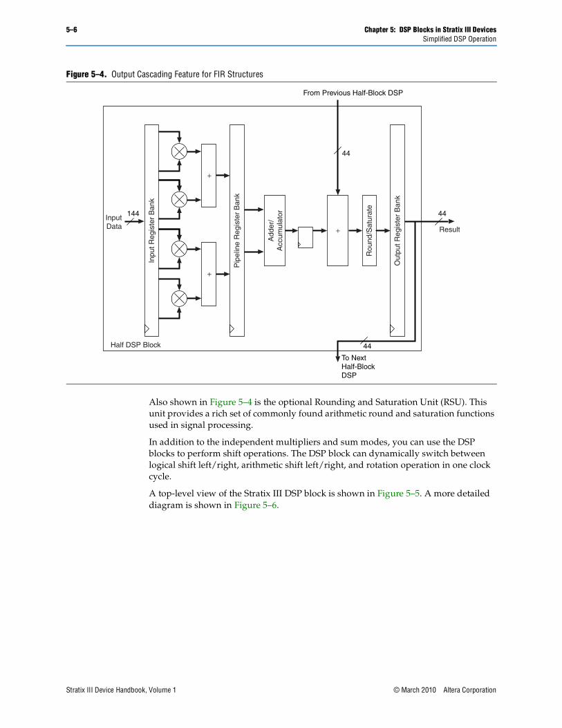
To support commonly found FIR-like structures efficiently, a major addition to the DSP block in Stratix III is the ability to propagate the result of one Half-Block to the next Half-Block completely within the DSP block without additional soft logic overhead. This is achieved by the inclusion of a dedicated addition unit and routing that adds the 44-bit result of a previous Half-Block with the 44-bit result of the current block. The 44-bit result is fed either to the next Half-Block or out of the DSP block through the output register stage. This is shown in Figure 5–4. Detailed examples are described in later sections.
The combination of a fast, low-latency Four-Multiplier Adder unit and the “chained cascade” capability of the output-chaining adder provide an optimal FIR and vector multiplication capability.
To support single-channel type FIR filters efficiently, you can configure one of the multiplier input’s registers to form a tap delay line input, saving resources and providing higher system performance.
Figure 5–3. Four-Multiplier Adder and Accumulation Capability
5–6 Chapter 5: DSP Blocks in Stratix III DevicesSimplified DSP Operation
Also shown in Figure 5–4 is the optional Rounding and Saturation Unit (RSU). This unit provides a rich set of commonly found arithmetic round and saturation functions used in signal processing.
In addition to the independent multipliers and sum modes, you can use the DSP blocks to perform shift operations. The DSP block can dynamically switch between logical shift left/right, arithmetic shift left/right, and rotation operation in one clock cycle.
A top-level view of the Stratix III DSP block is shown in Figure 5–5. A more detailed diagram is shown in Figure 5–6.
Figure 5–4. Output Cascading Feature for FIR Structures
5–8 Chapter 5: DSP Blocks in Stratix III DevicesOperational Modes Overview
Operational Modes OverviewEach Stratix III DSP block can be used in one of five basic operational modes. Table 5–2 lists the five basic operational modes and the number of multipliers that can be implemented within a single DSP block, depending on the mode.
The DSP block consists of two identical halves (top-half and bottom-half). Each half has four 18 × 18 multipliers.
The Quartus® II software includes megafunctions used to control the mode of operation of the multipliers. After making the appropriate parameter settings using the megafunction’s MegaWizardTM Plug-In Manager, the Quartus II software automatically configures the DSP block.
Stratix III DSP blocks can operate in different modes simultaneously. Each half-block is fully independent except for the sharing of the four clock, ena, and aclr signals. For example, you can break down a single DSP block to operate a 9 × 9 multiplier in one Half-Block and an 18 × 18 two-multiplier adder in the other Half-Block. This increases DSP block resource efficiency and allows you to implement more multipliers within a Stratix III device. The Quartus II software automatically places multipliers that can share the same DSP block resources within the same block.
Table 5–2. Stratix III DSP Block Operation Modes
Mode Multiplier in Width
# of Mults
# per Block
Signed or Unsigned
RND, SAT
In Shift Register
Chainout Adder
1st Stage Add/Sub
2nd Stage
Add/Acc
Independent Multiplier
9-bits 1 8 Both No No No — —
12-bits 1 6 Both No No No — —
18-bits 1 4 Both Yes Yes No — —
36-bits 1 2 Both No No No — —
Double 1 2 Both No No No — —
Two-Multiplier Adder(1) 18-bits 2 4 Signed (4) Yes No No Both —
Four-Multiplier Adder 18-bits 4 2 Both Yes Yes Yes Both Add Only
High Precision Multiplier Adder 18 × 36-bits 2 2 Both No No No — Add Only
Multiply Accumulate 18-bits 4 2 Both Yes Yes Yes Both Both
Shift (2) 36-bits (3) 1 2 Both No No — — —
Notes to Table 5–2:
(1) This mode also supports the loopback mode. In loopback mode, the number of loopback multipliers per DSP block is two and the remaining multipliers can be used in regular Two-Multiplier Adder mode.
(2) The dynamic shift mode supports arithmetic shift left, arithmetic shift right, logical shift left, logical shift right, and rotation operation.(3) The dynamic shift mode operates on a 32-bit input vector but the multiplier width is configured as 36-bits.(4) Unsigned value is also supported but you must make sure that the result can be contained within 36-bits.
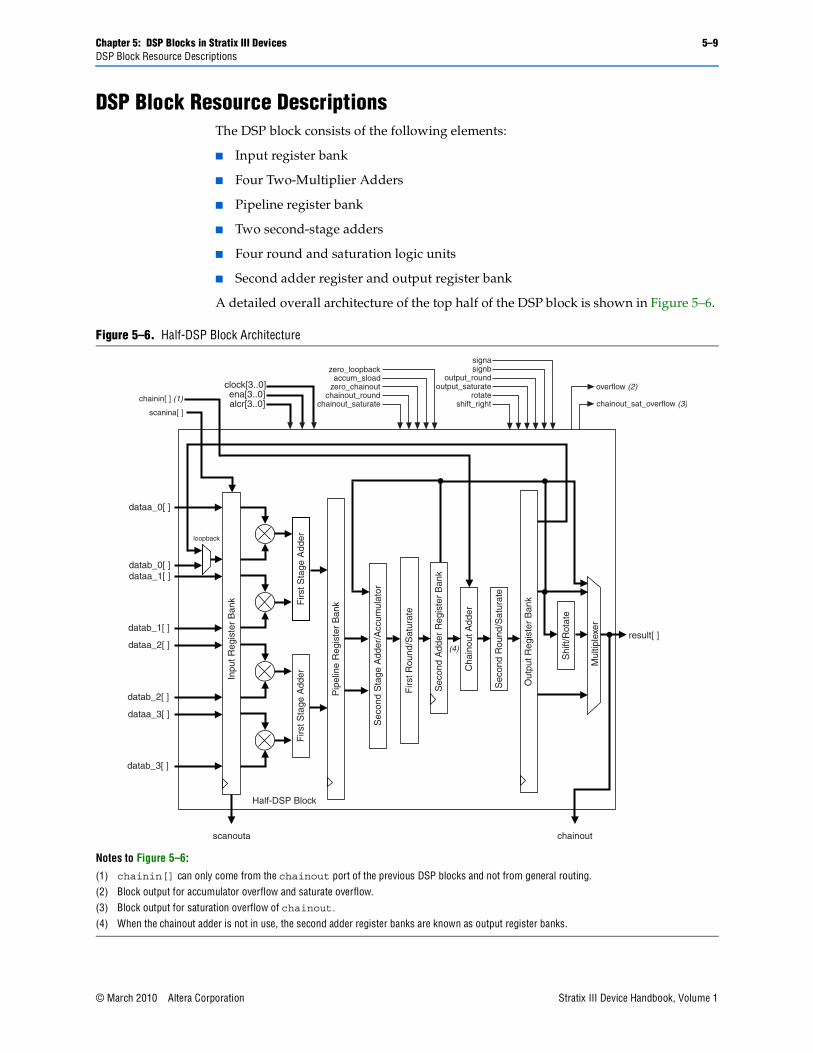
Chapter 5: DSP Blocks in Stratix III Devices 5–9DSP Block Resource Descriptions
DSP Block Resource DescriptionsThe DSP block consists of the following elements:
■ Input register bank
■ Four Two-Multiplier Adders
■ Pipeline register bank
■ Two second-stage adders
■ Four round and saturation logic units
■ Second adder register and output register bank
A detailed overall architecture of the top half of the DSP block is shown in Figure 5–6.
Figure 5–6. Half-DSP Block Architecture
Notes to Figure 5–6:
(1) chainin[] can only come from the chainout port of the previous DSP blocks and not from general routing.(2) Block output for accumulator overflow and saturate overflow.(3) Block output for saturation overflow of chainout.(4) When the chainout adder is not in use, the second adder register banks are known as output register banks.
5–10 Chapter 5: DSP Blocks in Stratix III DevicesDSP Block Resource Descriptions
Input RegistersAll of the DSP block registers are triggered by the positive edge of the clock signal and are cleared upon power up. Each multiplier operand can feed an input register or directly to the multiplier, bypassing the input registers. (This is configured at compile time.) The following DSP block signals control the input registers within the DSP block:
■ clock[3..0]
■ ena[3..0]
■ aclr[3..0]
Every DSP block has nine 18-bit data input register banks per half DSP block. Every half DSP block has the option to use the eight data register banks as inputs to the four multipliers. The special ninth register bank is a delay register required by modes that use both the cascade and chainout features of the DSP block and is for balancing the latency requirements when using the chained cascade feature.
A feature of the input register bank is to support a tap delay line. Therefore, the top leg of the multiplier input (A) could be driven from general routing or from the cascade chain, as shown in Figure 5–7.
Chapter 5: DSP Blocks in Stratix III Devices 5–11DSP Block Resource Descriptions
You must select whether the A-input comes from general routing or from the cascade chain at compile time. In cascade mode, the dedicated shift outputs from one multiplier block directly feeds input registers of the adjacent multiplier below it (within the same half DSP block) or the first multiplier in the next half DSP block, to form an 8-tap shift register chain per DSP Block. The DSP block can increase the length of the shift register chain by cascading to the lower DSP blocks. The dedicated shift register chain spans a single column, but you can implement longer shift register chains requiring multiple columns using the regular FPGA routing resources.
5–12 Chapter 5: DSP Blocks in Stratix III DevicesDSP Block Resource Descriptions
Shift registers are useful in DSP functions such as FIR filters. When implementing 18 × 18 or smaller width multipliers, you do not need external logic to create the shift register chain because the input shift registers are internal to the DSP block. This implementation significantly reduces the logical element (LE) resources required, avoids routing congestion, and results in predictable timing.
The first multiplier in every half DSP block (top- and bottom-half) in Stratix III devices has a multiplexer for the first multiplier B-input (lower-leg input) register to select between general routing and loopback, as shown in Figure 5–6. In loopback mode, the most significant 18-bit registered outputs are connected as feedback to the multiplier input of the first top multiplier in each half DSP block. Loopback modes are used by recursive filters where the previous output is needed to compute the current output.
The loopback mode is described in detail in “Two-Multiplier Adder Sum Mode” on page 5–21.
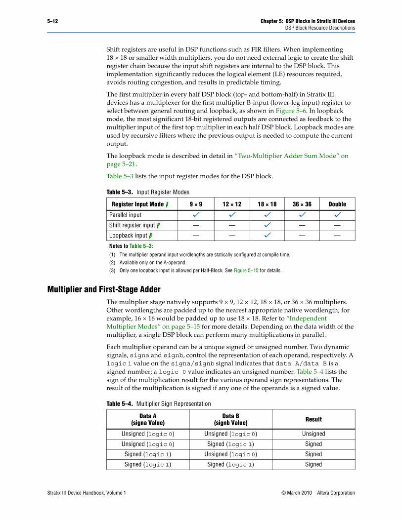
Table 5–3 lists the input register modes for the DSP block.
Multiplier and First-Stage AdderThe multiplier stage natively supports 9 × 9, 12 × 12, 18 × 18, or 36 × 36 multipliers. Other wordlengths are padded up to the nearest appropriate native wordlength; for example, 16 × 16 would be padded up to use 18 × 18. Refer to “Independent Multiplier Modes” on page 5–15 for more details. Depending on the data width of the multiplier, a single DSP block can perform many multiplications in parallel.
Each multiplier operand can be a unique signed or unsigned number. Two dynamic signals, signa and signb, control the representation of each operand, respectively. A logic 1 value on the signa/signb signal indicates that data A/data B is a signed number; a logic 0 value indicates an unsigned number. Table 5–4 lists the sign of the multiplication result for the various operand sign representations. The result of the multiplication is signed if any one of the operands is a signed value.
Notes to Table 5–3:(1) The multiplier operand input wordlengths are statically configured at compile time.(2) Available only on the A-operand.(3) Only one loopback input is allowed per Half-Block. See Figure 5–15 for details.
Chapter 5: DSP Blocks in Stratix III Devices 5–13DSP Block Resource Descriptions
Each Half Block has its own signa and signb signal. Therefore, all of the data A inputs feeding the same DSP Half Block must have the same sign representation. Similarly, all of the data B inputs feeding the same DSP Half Block must have the same sign representation. The multiplier offers full precision regardless of the sign representation in all operational modes except for full precision 18 x 18 loopback and Two-Multiplier Adder modes. Refer to “Two-Multiplier Adder Sum Mode” on page 5–21 for details.
1 When the signa and signb signals are unused, the Quartus II software sets the multiplier to perform unsigned multiplication by default.
The outputs of the multipliers are the only outputs that can feed into the first-stage adder, as shown in Figure 5–6. There are four first-stage adders in a DSP block (two adders per half DSP block). The first-stage adder block has the ability to perform addition and subtraction. The control signal for addition or subtraction is static and has to be configured upon compile time. The first-stage adders are used by the sum modes to compute the sum of two multipliers, 18 × 18-complex multipliers, and to perform the first stage of a 36 × 36 multiply and shift operation.
Depending on your specifications, the output of the first-stage adder has the option to feed into the pipeline registers, second-stage adder, round and saturation unit, or the output registers.
Pipeline Register StageThe output from the first-stage adder can either feed or bypass the pipeline registers, as shown in Figure 5–6. Pipeline registers increase the DSP block’s maximum performance (at the expense of extra cycles of latency), especially when using the subsequent DSP block stages. Pipeline registers split up the long signal path between the input-registers/multiplier/first-stage adder and the second-stage adder/round-and-saturation/output-registers, creating two shorter paths.
Second-Stage AdderThere are four individual 44-bit second-stage adders per DSP block (2 adders per half DSP block). You can configure the second-stage adders as follows:
■ The final stage of a 36-bit multiplier
■ A sum of four (18 × 18)
■ An accumulator (44-bits maximum)
■ A chained output summation (44-bits maximum)
1 The chained-output adder can be used at the same time as a second-level adder in chained output summation mode.
1 The output of the second-stage adder has the option to go into the round and saturation logic unit or the output register.
1 You cannot use the second-stage adder independently from the multiplier and first-stage adder.
5–14 Chapter 5: DSP Blocks in Stratix III DevicesDSP Block Resource Descriptions
Round and Saturation StageThe round and saturation logic units are located at the output of the 44-bit second-stage adder (round logic unit followed by the saturation logic unit). There are two round and saturation logic units per half DSP block. The input to the round and saturation logic unit can come from one of the following stages:
■ Output of the multiplier (independent multiply mode in 18 × 18)
■ Output of the first-stage adder (Two-Multiplier Adder)
■ Output of the pipeline registers
■ Output of the second-stage adder (Four-Multiplier Adder, Multiply-Accumulate Mode in 18 × 18)
These stages are discussed in detail in “Operational Mode Descriptions” on page 5–15.
The round and saturation logic unit is controlled by the dynamic round and saturate signals, respectively. A logic 1 value on the round, saturate, or both enables the round, saturate, or both logic units.
1 You can use the round and saturation logic units together or independently.
Second Adder and Output RegistersThe second adder register and output register banks are two banks of 44-bit registers that can also be combined to form larger 72-bit banks to support 36 × 36 output results.
The outputs of the different stages in the Stratix III devices are routed to the output registers through an output selection unit. Depending on the operational mode of the DSP block, the output selection unit selects whether the outputs of the DSP blocks comes from the outputs of the multiplier block, first-stage adder, pipeline registers, second-stage adder, or the round and saturation logic unit. The output selection unit is set automatically by the software, based on the DSP block operational mode you specified, and has the option to either drive or bypass the output registers. The exception is when the block is used in shift mode, in which case the user dynamically controls the output-select multiplexer directly.
When the DSP block is configured in “chained cascaded” output mode, both of the second-stage adders are used. The first one is used for performing Four-Multiplier Adder and the second is used for the chainout adder. The outputs of the Four-Multiplier Adder are routed to the second-stage adder registers before it enters the chainout adder. The output of the chainout adder goes to the regular output register bank. Depending on the configuration, the chainout results can be routed to the input of the next half-block’s chainout adder input or to the general fabric (functioning as regular output registers). Refer to “Operational Mode Descriptions” on page 5–15 for details.
Chapter 5: DSP Blocks in Stratix III Devices 5–15Operational Mode Descriptions
The second-stage and output registers are triggered by the positive edge of the clock signal and are cleared on power up. The following DSP block signals control the output registers within the DSP block:
■ clock[3..0]
■ ena[3..0]
■ aclr[3..0]
Operational Mode DescriptionsThe various modes of operation are discussed below.
Independent Multiplier ModesIn independent input and output multiplier mode, the DSP block performs individual multiplication operations for general-purpose multipliers.
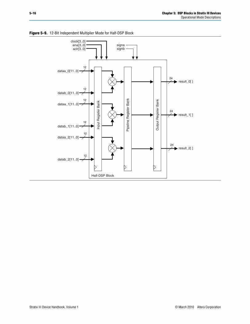
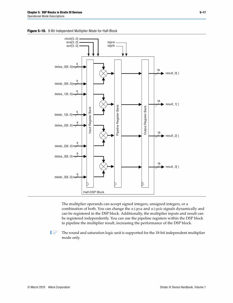
9-, 12-, and 18-Bit MultiplierYou can configure each DSP block multiplier for 9-, 12-, or 18-bit multiplication. A single DSP block can support up to eight individual 9 × 9 multipliers, six 12 × 12 multipliers, or up to four individual 18 × 18 multipliers. For operand widths up to 9 bits, a 9 × 9 multiplier is implemented. For operand widths from 10 to 12 bits, a 12 × 12 multiplier is implemented, and for operand widths from 13 to 18 bits, an 18 × 18 multiplier is implemented. This is done by the Quartus II software by zero-padding the LSBs. Figure 5–8, Figure 5–9, and Figure 5–10 show the DSP block in the independent multiplier operation mode.
Figure 5–8. 18-Bit Independent Multiplier Mode for Half-DSP Block
Chapter 5: DSP Blocks in Stratix III Devices 5–17Operational Mode Descriptions
The multiplier operands can accept signed integers, unsigned integers, or a combination of both. You can change the signa and signb signals dynamically and can be registered in the DSP block. Additionally, the multiplier inputs and result can be registered independently. You can use the pipeline registers within the DSP block to pipeline the multiplier result, increasing the performance of the DSP block.
1 The round and saturation logic unit is supported for the 18-bit independent multiplier mode only.
Figure 5–10. 9-Bit Independent Multiplier Mode for Half-Block
5–18 Chapter 5: DSP Blocks in Stratix III DevicesOperational Mode Descriptions
36-Bit MultiplierYou can efficiently construct a 36 × 36 multiplier using four 18 × 18 multipliers. This simplification fits conveniently into one half-DSP block, and is implemented in the DSP block automatically by selecting the 36 × 36 mode. Stratix III devices can have up to two 36-bit multipliers per DSP block (one 36-bit multiplier per half DSP block). The 36-bit multiplier is also under the independent multiplier mode but uses the entire half DSP block, including the dedicated hardware logic after the pipeline registers to implement the 36 × 36 bit multiplication operation. This is shown in Figure 5–11.
The 36-bit multiplier is useful for applications requiring more than 18-bit precision; for example, for the mantissa multiplication portion of single precision and extended single precision floating-point arithmetic applications.
Figure 5–11. 36-Bit Independent Multiplier Mode for Half-DSP Block
Chapter 5: DSP Blocks in Stratix III Devices 5–19Operational Mode Descriptions
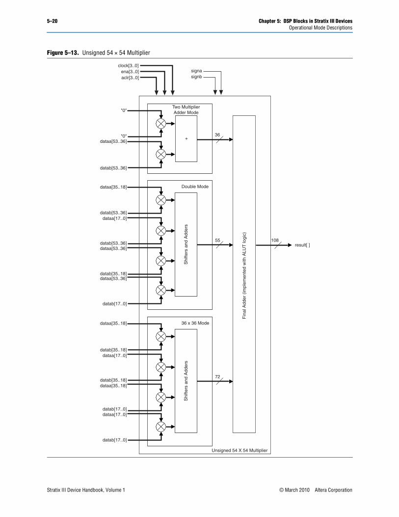
Double MultiplierThe Stratix III DSP block can be configured to efficiently support an unsigned 54 × 54 bit multiplier that is required to compute the mantissa portion of an IEEE double precision floating point multiplication. A 54 × 54 bit multiplier can be built using basic 18 × 18 multipliers, shifters, and adders. In order to efficiently utilize the Stratix III DSP block's built in shifters and adders, a special Double mode (partial 54 × 54 multiplier) is available that is a slight modification to the basic 36 × 36 Multiplier mode. This is shown in Figure 5–12 and Figure 5–13.
Chapter 5: DSP Blocks in Stratix III Devices 5–21Operational Mode Descriptions
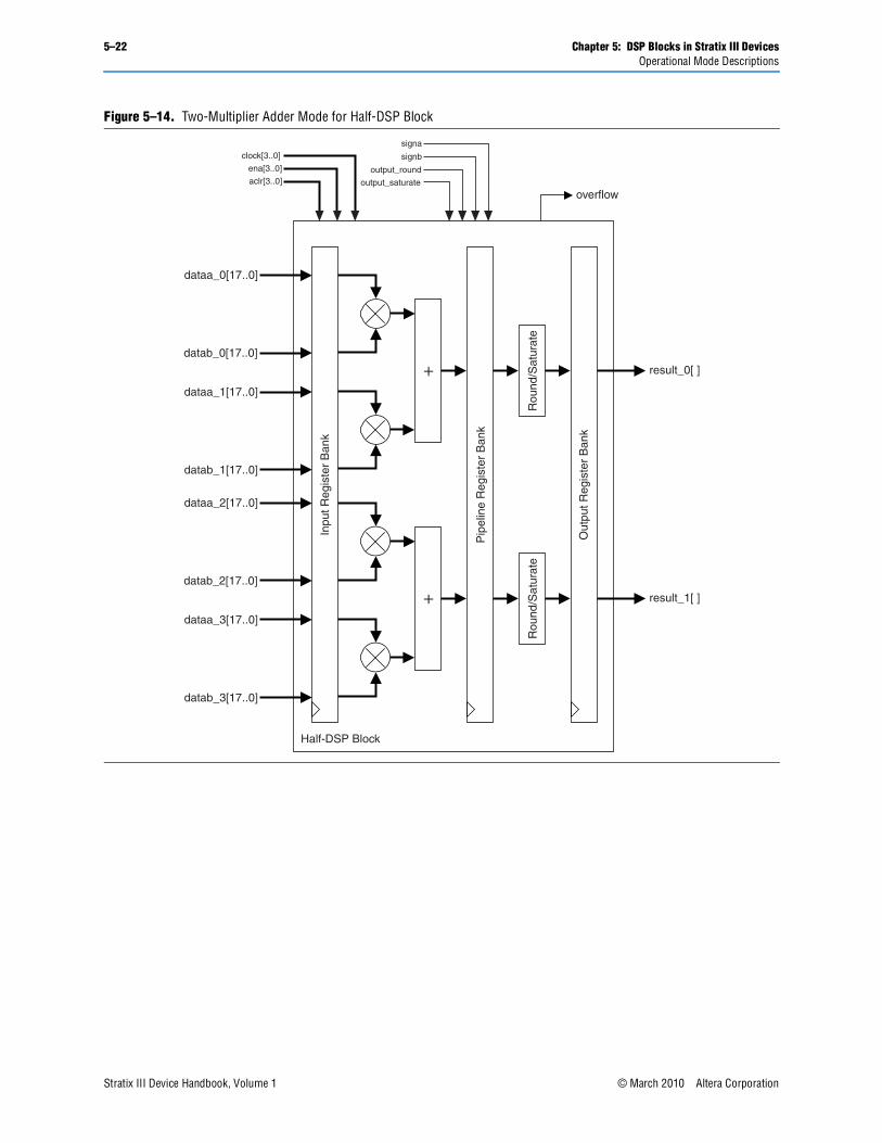
Two-Multiplier Adder Sum ModeIn the two-multiplier adder configuration, the DSP block can implement four 18-bit Two-Multiplier Adders (2 Two-Multiplier Adders per half DSP block). You can configure the adders to take the sum or difference of two multiplier outputs. Summation or subtraction has to be selected at compile time. The Two-Multiplier Adder function is useful for applications such as FFTs, complex FIR, and IIR filters. Figure 5–14 shows the DSP block configured in the two-multiplier adder mode.
The loopback mode is the other sub-feature of the two-multiplier adder mode. Figure 5–15 shows the DSP block configured in the loopback mode. This mode takes the 36-bit summation result of the two multipliers and feeds back the most significant 18-bits to the input. The lower 18-bits are discarded. You have the option to disable or zero-out the loopback data by using the dynamic zero_loopback signal. A logic 1 value on the zero_loopback signal selects the zeroed data or disables the looped back data, while a logic 0 selects the looped back data.
1 The option to use the loopback mode or the general two-multiplier adder mode must be selected at compile time.
For the Two-Multiplier Adder mode, if all the inputs are full 18-bit and unsigned, the result will require 37 bits. As the output data width in Two-Multiplier Adder mode is limited to 36 bits, this 37-bit output requirement is not allowed. Any other combination that does not violate the 36-bit maximum result is permitted; for example, two 16 × 16 signed Two-Multiplier Adders is valid.
The two-multiplier adder mode supports the round and saturation logic unit. You can use the pipeline registers and output registers within the DSP block to pipeline the multiplier-adder result, increasing the performance of the DSP block.
5–24 Chapter 5: DSP Blocks in Stratix III DevicesOperational Mode Descriptions
18 × 18 Complex MultiplyYou can configure the DSP block when used in Two-Multiplier Adder mode to implement complex multipliers using the two-multiplier adder mode. A single half DSP block can implement one 18-bit complex multiplier.
A complex multiplication can be written as shown in Equation 5–4.
To implement this complex multiplication within the DSP block, the real part ((a × c) – (b × d)) is implemented using two multipliers feeding one subtractor block while the imaginary part ((a × d) + (b × c)) is implemented using another two multipliers feeding an adder block. Figure 5–16 shows an 18-bit complex multiplication. This mode automatically assumes all inputs are using signed numbers.
Chapter 5: DSP Blocks in Stratix III Devices 5–25Operational Mode Descriptions
Four-Multiplier AdderIn the four-multiplier adder configuration shown in Figure 5–17, the DSP block can implement two four-multiplier adders (one four-multiplier adder per half DSP block). These modes are useful for implementing one-dimensional and two-dimensional filtering applications. The four-multiplier adder is performed in two addition stages. The outputs of two of the four multipliers are initially summed in the two first-stage adder blocks. The results of these two adder blocks are then summed in the second-stage adder block to produce the final four-multiplier adder result, as shown by Equation 5–2 and Equation 5–3.
The four-multiplier adder mode supports the round and saturation logic unit. You can use the pipeline registers and output registers within the DSP block to pipeline the multiplier-adder result, increasing the performance of the DSP block.
Figure 5–17. Four-Multiplier Adder Mode for Half-DSP Block
5–26 Chapter 5: DSP Blocks in Stratix III DevicesOperational Mode Descriptions
High Precision Multiplier AdderIn the high precision multiplier adder configuration shown in Figure 5–18, the DSP block can implement two two-multiplier adders, with multiplier precision of 18 × 36 (one two-multiplier adder per DSP half block). This mode is useful in filtering or FFT applications where a data path greater than 18 bits is required, yet 18 bits is sufficient for the coefficient precision. This can occur in cases where that data has a high dynamic range. If the coefficients are fixed, as in FFT and most filter applications, the precision of 18 bits will provide a dynamic range over 100 dB if the largest coefficient is normalized to the maximum 18-bit representation.
In these situations, the data path can be up to 36 bits, allowing ample headroom to bit growth, or gain changes in the signal source without loss of precision. This mode is also extremely useful in single precision block floating point applications.
The high precision multiplier adder is preformed in two stages. The 18 × 36 multiply is decomposed into two 18 × 18 multipliers. The multiplier with the LSB of the data source is performed unsigned, while the multiplier with the MSB of the data source can be signed or signed. The latter multiplier has its result left shifted by 18 bits prior to the first adder stage, creating an effective 18 × 36 multiplier. The results of these two adder blocks are then summed in the second stage adder block to produce the final result.
Equation 5–5. High Precision Multiplier Adder Equation
5–28 Chapter 5: DSP Blocks in Stratix III DevicesOperational Mode Descriptions
Multiply Accumulate ModeIn multiply accumulate mode, the second-stage adder is configured as a 44-bit accumulator or subtractor. The output of the DSP block is looped back to the second-stage adder and added or subtracted with the two outputs of the first-stage adder block according to Equation 5–3. Figure 5–19 shows the DSP block configured to operate in multiply accumulate mode.
Figure 5–19. Multiply Accumulate Mode for Half-DSP Block
Chapter 5: DSP Blocks in Stratix III Devices 5–29Operational Mode Descriptions
A single DSP block can implement up to two independent 44-bit accumulators.
The dynamic accum_sload control signal is used to clear the accumulation. A logic 1 value on the accum_sload signal synchronously loads the accumulator with the multiplier result only, while a logic 0 enables accumulation by adding or subtracting the output of the DSP block (accumulator feedback) to the output of the multiplier and first-stage adder.
1 The control signal for the accumulator and subtractor is static and therefore has to be configured at compile time.
This mode supports the round and saturation logic unit as it is configured as an 18-bit multiplier accumulator. You can use the pipeline registers and output registers within the DSP block to increase the performance of the DSP block.
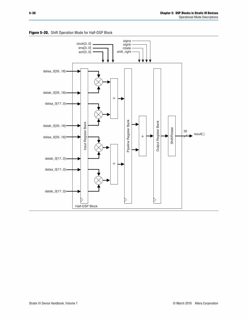
Shift ModesStratix III devices support the following shift modes for 32-bit input only:
■ Arithmetic shift left, ASL[N]
■ Arithmetic shift right, ASR[32-N]
■ Logical shift left, LSL[N]
■ Logical shift right, LSR[32-N]
■ 32-bit rotator or Barrel shifter, ROT[N]
1 You can switch the shift mode between these modes using the dynamic rotate and shift control signals.
The shift mode in a Stratix III device can be easily used by the soft embedded processor such as Nios® II to perform the dynamic shift and rotate operation. Figure 5–20 shows the shift mode configuration.
The shift mode makes use of the available multipliers to logically or arithmetically shift left, right, or rotate the desired 32-bit data. The DSP block is configured like the independent 36-bit multiplier mode to perform the shift mode operations.
The arithmetic shift right requires signed input vector. During arithmetic shift right, the sign is extended to fill the MSB of the 32-bit vector. The logical shift right uses unsigned input vector. During logical shift right, zeros are padded in the most significant bits shifting the 32-bit vector to the right. The barrel shifter uses unsigned input vector and implements a rotation function on a 32-bit word length.
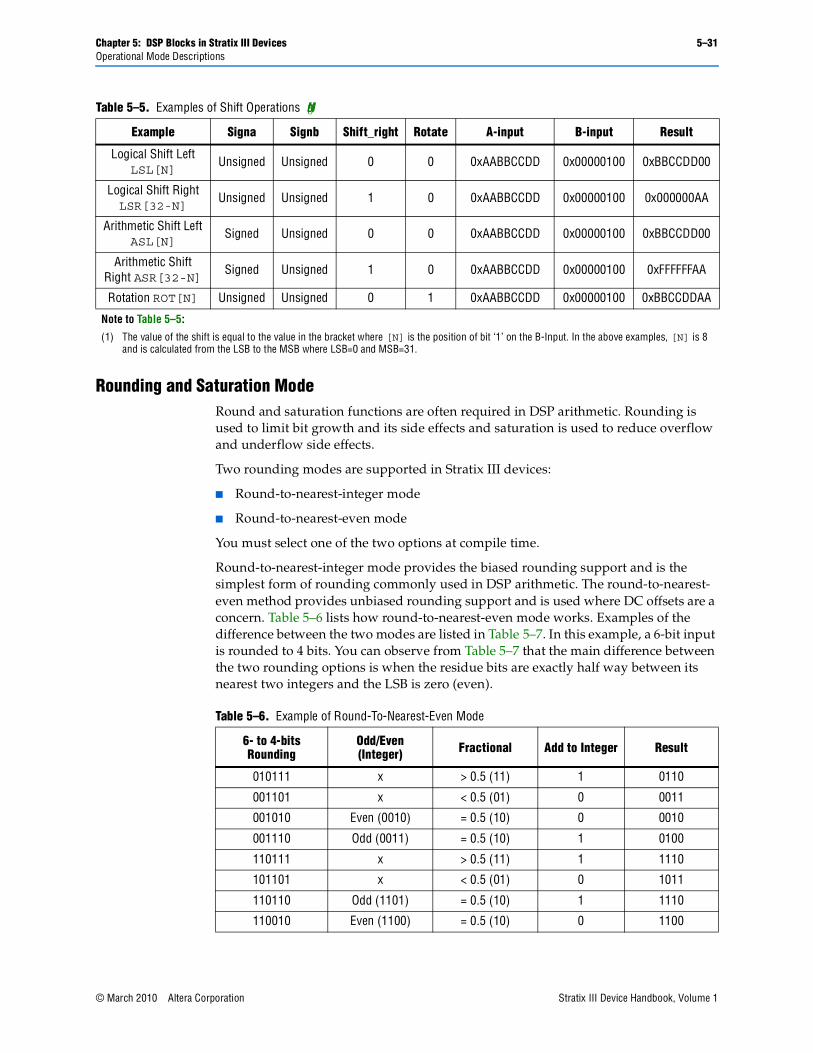
Two control signals rotate and shift_right together with the signa and signb signals, determining the shifting operation. Examples of shift operations are listed in Table 5–5 on page 5–31.
Chapter 5: DSP Blocks in Stratix III Devices 5–31Operational Mode Descriptions
Rounding and Saturation ModeRound and saturation functions are often required in DSP arithmetic. Rounding is used to limit bit growth and its side effects and saturation is used to reduce overflow and underflow side effects.
Two rounding modes are supported in Stratix III devices:
■ Round-to-nearest-integer mode
■ Round-to-nearest-even mode
You must select one of the two options at compile time.
Round-to-nearest-integer mode provides the biased rounding support and is the simplest form of rounding commonly used in DSP arithmetic. The round-to-nearest-even method provides unbiased rounding support and is used where DC offsets are a concern. Table 5–6 lists how round-to-nearest-even mode works. Examples of the difference between the two modes are listed in Table 5–7. In this example, a 6-bit input is rounded to 4 bits. You can observe from Table 5–7 that the main difference between the two rounding options is when the residue bits are exactly half way between its nearest two integers and the LSB is zero (even).
Table 5–5. Examples of Shift Operations (Note 1)
Example Signa Signb Shift_right Rotate A-input B-input Result
(1) The value of the shift is equal to the value in the bracket where [N] is the position of bit ‘1’ on the B-Input. In the above examples, [N] is 8 and is calculated from the LSB to the MSB where LSB=0 and MSB=31.
Table 5–6. Example of Round-To-Nearest-Even Mode
6- to 4-bits Rounding
Odd/Even (Integer) Fractional Add to Integer Result
5–32 Chapter 5: DSP Blocks in Stratix III DevicesOperational Mode Descriptions
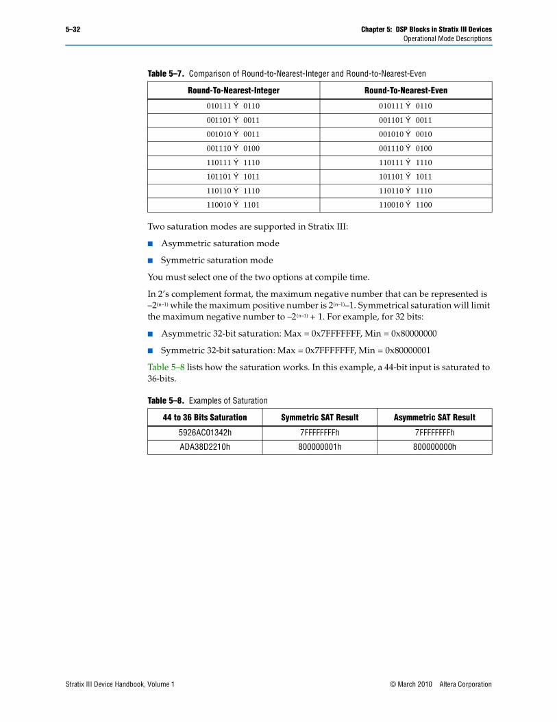
Two saturation modes are supported in Stratix III:
■ Asymmetric saturation mode
■ Symmetric saturation mode
You must select one of the two options at compile time.
In 2’s complement format, the maximum negative number that can be represented is –2(n–1) while the maximum positive number is 2(n–1)–1. Symmetrical saturation will limit the maximum negative number to –2(n–1) + 1. For example, for 32 bits:
■ Asymmetric 32-bit saturation: Max = 0x7FFFFFFF, Min = 0x80000000
■ Symmetric 32-bit saturation: Max = 0x7FFFFFFF, Min = 0x80000001
Table 5–8 lists how the saturation works. In this example, a 44-bit input is saturated to 36-bits.
Table 5–7. Comparison of Round-to-Nearest-Integer and Round-to-Nearest-Even
Round-To-Nearest-Integer Round-To-Nearest-Even
Table 5–8. Examples of Saturation
44 to 36 Bits Saturation Symmetric SAT Result Asymmetric SAT Result
Chapter 5: DSP Blocks in Stratix III Devices 5–33Operational Mode Descriptions
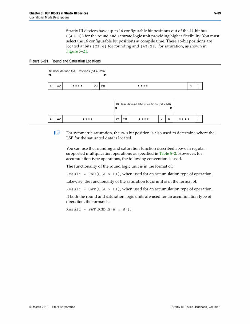
Stratix III devices have up to 16 configurable bit positions out of the 44-bit bus ([43:0]) for the round and saturate logic unit providing higher flexibility. You must select the 16 configurable bit positions at compile time. These 16-bit positions are located at bits [21:6] for rounding and [43:28] for saturation, as shown in Figure 5–21.
1 For symmetric saturation, the RND bit position is also used to determine where the LSP for the saturated data is located.
You can use the rounding and saturation function described above in regular supported multiplication operations as specified in Table 5–2. However, for accumulation type operations, the following convention is used.
The functionality of the round logic unit is in the format of:
Result = RND[S(A × B)], when used for an accumulation type of operation.
Likewise, the functionality of the saturation logic unit is in the format of:
Result = SAT[S(A × B)], when used for an accumulation type of operation.
If both the round and saturation logic units are used for an accumulation type of operation, the format is:
5–34 Chapter 5: DSP Blocks in Stratix III DevicesOperational Mode Descriptions
DSP Block Control SignalsThe Stratix III DSP block is configured using a set of static and dynamic signals. The DSP block dynamic signals are user configurable and can be set to toggled or not at run time. Table 5–10 lists the dynamic signals for the DSP block.
Table 5–10. DSP Block Dynamic Signals (Part 1 of 2)
Signal Name Function Count
■ signa
■ signb
Signed/unsigned control for all multipliers and adders.
signa for “multiplicand” input bus to dataa[17:0] each multiplier.
signb for “multiplier” input bus datab[17:0] to each multiplier.
signa = 1, signb = 1 for signed-signed multiplication
signa = 1, signb = 0 for signed-unsigned multiplication
signa = 0, signb = 1 for unsigned-signed multiplication
signa = 0, signb = 0 for unsigned-unsigned multiplication
2
output_round
Round control for first stage round/saturation block. output_round = 1 for rounding on multiply output
output_round = 0 for normal multiply output1
chainout_round
Round control for second stage round/saturation block. chainout_round = 1 for rounding on multiply output
chainout_round = 0 for normal multiply output1
output_saturate
Saturation control for first stage round/saturation block for Q-format multiply. If both rounding and saturation is enabled, saturation is done on the rounded result.
output_saturate = 1 for saturation support
output_saturate = 0 for no saturation support
1
chainout_saturate
Saturation control for second stage round/saturation block for Q-format multiply. If both rounding and saturation are enabled, saturation is done on the rounded result.
chainout_saturate = 1 for saturation support
chainout_saturate = 0 for no saturation support
1
accum_sload
Dynamically specifies whether the accumulator value is zero. accum_sload = 0, accumulation input is from the output registers
accum_sload = 1, accumulation input is set to be zero1
zero_chainout Dynamically specifies whether the chainout value is zero. 1
zero_loopback Dynamically specifies whether the loopback value is zero. 1
rotate rotation = 1, rotation feature is enabled 1
shift_right shift_right = 1, shift right feature is enabled 1
Chapter 5: DSP Blocks in Stratix III Devices 5–35Application Examples
Application Examples
FIR ExampleA finite impulse response filter is a common function used in many systems to perform spectral manipulations. The basic form is shown in Equation 5–6.
In this equation, x(n) is the input samples to the filter, c(k) are the filter coefficients, and y(n) are the filtered output samples. Typically, the coefficients do not change in time in most applications such as Digital Down Converters (DDC). FIR filters can be implemented in many forms, the most simple being the tap-delay line approach.
Stratix III DSP block can implement various types of FIR filters very efficiently. To form the tap-delay line, the input register stage of the DSP block has the ability to cascade the input in a chained fashion in 18-bit wide format. Unlike the Stratix II DSP block, which has two built-in parallel input register scan paths, Stratix III supports only one built-in 18-bit parallel input register scan path for 288 data input.
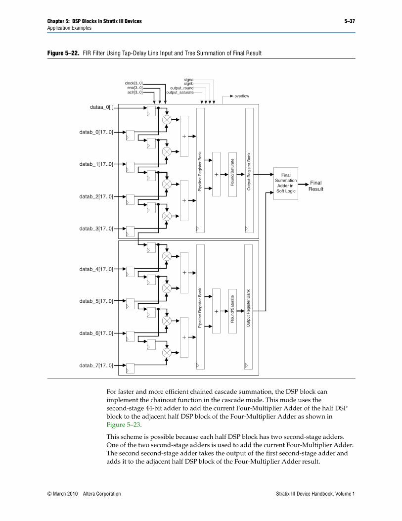
For a pair of 18-bit input buses, the A input for the first 18-bit bus is fed back to be registered again at the input of the second (lower) pair of inputs. Refer to Figure 5–22 for details.
The B input of the multiplier feeds from the general routing. You can scan in the data in 18-bit parallel form and multiply it by the 18-bit input bus from general routing in each cycle.
5–36 Chapter 5: DSP Blocks in Stratix III DevicesApplication Examples
Normally in a FIR filter, the fixed data input (from general routing and not from cascade) is the constant that needs to be multiplied by the cascaded input. In 18-bit mode, the DSP block has enough input registers to register the general routing signals and the cascaded signal buses before multiplying them. This makes having eight taps for an 18-bit cascade mode possible. Each tap can be considered a single multiplier. If all eight multiplier inputs for the full DSP block are cascaded in a parallel scan chain, an eight-tap FIR filter is created, as shown in Figure 5–22.
The DSP block can be concatenated to have more than eight taps by enabling the option to output the parallel scan chain to the next (lower) DSP block. Likewise, the output of previous (above) cascade chain is used as an input to the current block. The first (top) multiplier in each half block will have the option to select the 18-bit cascade chain input from the regular routing or from the previous (above) cascade chain. Also, the last cascaded chain in each half DSP block can exit the DSP block by routing the cascade chain after the last (fourth from top) input register to the output routing channel, bypassing both the pipeline and output registers. This concatenation allows the user to easily construct their desired filter length.
You can use the Four-Multiplier Adder mode with one of the inputs to each multiplier being in a form of chained cascaded input from the previous (above) register. This is very similar to the regular Four-Multiplier Adder with the difference being that not all the inputs are from general routing.
For a complete FIR, the results per individual Four-Multiplier Adder can be combined in either a tree or chained cascade manner. Using external logic and adders, you can very easily implement a tree summation, as shown in Figure 5–22.
Chapter 5: DSP Blocks in Stratix III Devices 5–37Application Examples
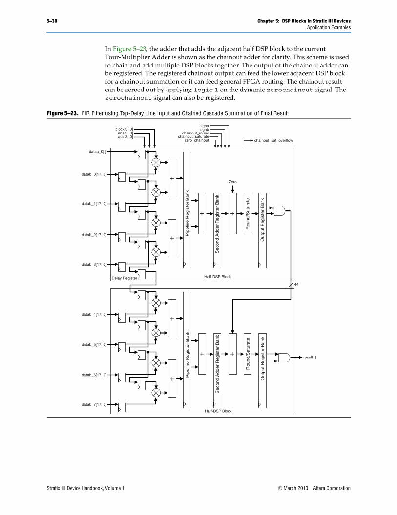
For faster and more efficient chained cascade summation, the DSP block can implement the chainout function in the cascade mode. This mode uses the second-stage 44-bit adder to add the current Four-Multiplier Adder of the half DSP block to the adjacent half DSP block of the Four-Multiplier Adder as shown in Figure 5–23.
This scheme is possible because each half DSP block has two second-stage adders. One of the two second-stage adders is used to add the current Four-Multiplier Adder. The second second-stage adder takes the output of the first second-stage adder and adds it to the adjacent half DSP block of the Four-Multiplier Adder result.
Figure 5–22. FIR Filter Using Tap-Delay Line Input and Tree Summation of Final Result
5–38 Chapter 5: DSP Blocks in Stratix III DevicesApplication Examples
In Figure 5–23, the adder that adds the adjacent half DSP block to the current Four-Multiplier Adder is shown as the chainout adder for clarity. This scheme is used to chain and add multiple DSP blocks together. The output of the chainout adder can be registered. The registered chainout output can feed the lower adjacent DSP block for a chainout summation or it can feed general FPGA routing. The chainout result can be zeroed out by applying logic 1 on the dynamic zerochainout signal. The zerochainout signal can also be registered.
Figure 5–23. FIR Filter using Tap-Delay Line Input and Chained Cascade Summation of Final Result
Chapter 5: DSP Blocks in Stratix III Devices 5–39Application Examples
When you use both the input cascade and chainout features, the DSP block uses an 18-bit delay register in the boundary of each half-DSP block or from block-to-block to synchronize the input scan chain data with the chainout data. The top half computes the sum of product and chains the output to the next block after the output register. The output register uses the delay register to delay the cascade input by one clock cycle to compensate the latency for the bottom half.
For applications in which the system clock is slower than the speed of the DSP block, the multipliers can be time-multiplexed to improve efficiency. This makes multi-channel and semi-parallel FIR structures possible. The structure to achieve this is similar to Figure 5–22 and Figure 5–23. The main difference is that the input cascade chain is no longer used and each half-DSP block is used in Four-Multiplier Mode with independent inputs. Figure 5–24 shows an example for chained cascaded summation.
In most cases, only the final stage FIR tap with the rounding and saturation unit is deployed.
5–40 Chapter 5: DSP Blocks in Stratix III DevicesApplication Examples
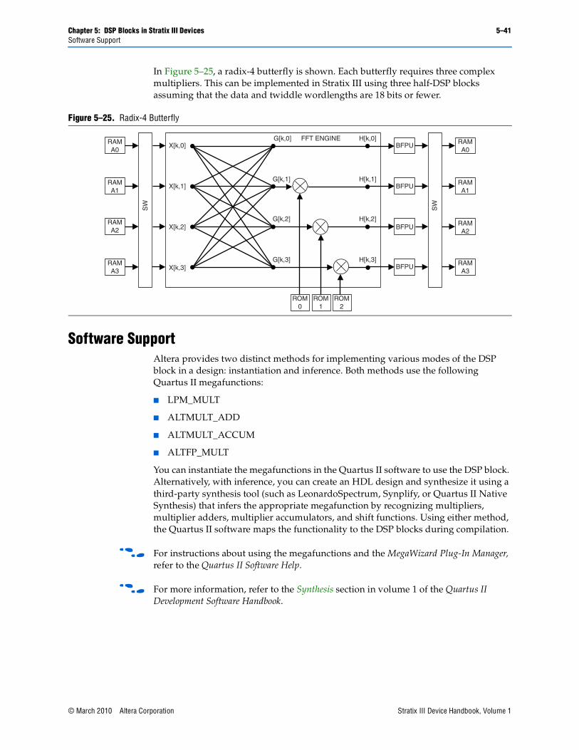
FFT ExampleThe Fast Fourier Transform (FFT) is a very common DSP function used to convert samples in the time domain to and from the frequency domain. A fundamental building block of the FFT is the FFT butterfly. FFTs are most efficient when operating on complex samples. You can use the Stratix III DSP block to form the core of a complex FFT butterfly very efficiently.
Figure 5–24. Semi-Parallel FIR Structure Using Chained Cascaded Summation
Chapter 5: DSP Blocks in Stratix III Devices 5–41Software Support
In Figure 5–25, a radix-4 butterfly is shown. Each butterfly requires three complex multipliers. This can be implemented in Stratix III using three half-DSP blocks assuming that the data and twiddle wordlengths are 18 bits or fewer.
Software SupportAltera provides two distinct methods for implementing various modes of the DSP block in a design: instantiation and inference. Both methods use the following Quartus II megafunctions:
■ LPM_MULT
■ ALTMULT_ADD
■ ALTMULT_ACCUM
■ ALTFP_MULT
You can instantiate the megafunctions in the Quartus II software to use the DSP block. Alternatively, with inference, you can create an HDL design and synthesize it using a third-party synthesis tool (such as LeonardoSpectrum, Synplify, or Quartus II Native Synthesis) that infers the appropriate megafunction by recognizing multipliers, multiplier adders, multiplier accumulators, and shift functions. Using either method, the Quartus II software maps the functionality to the DSP blocks during compilation.
f For instructions about using the megafunctions and the MegaWizard Plug-In Manager, refer to the Quartus II Software Help.
f For more information, refer to the Synthesis section in volume 1 of the Quartus II Development Software Handbook.