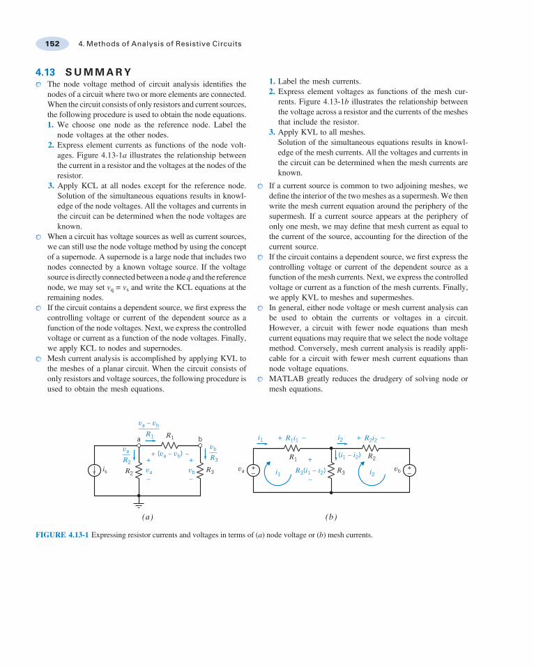
4.13 SUMMARY The node voltage method of circuit analysis identifies the nodes of a circuit where two or more elements are connected. When the circuit consists of only resistors and current sources, the following procedure is used to obtain the node equations. 1. We choose one node as the reference node. Label the node voltages at the other nodes. 2. Express element currents as functions of the node volt- ages. Figure 4.13-1a illustrates the relationship between the current in a resistor and the voltages at the nodes of the resistor. 3. Apply KCL at all nodes except for the reference node. Solution of the simultaneous equations results in knowl- edge of the node voltages. All the voltages and currents in the circuit can be determined when the node voltages are known. When a circuit has voltage sources as well as current sources, we can still use the node voltage method by using the concept of a supernode. A supernode is a large node that includes two nodes connected by a known voltage source. If the voltage source is directly connected between a node q and the reference node, we may set v q = v s and write the KCL equations at the remaining nodes. If the circuit contains a dependent source, we first express the controlling voltage or current of the dependent source as a function of the node voltages. Next, we express the controlled voltage or current as a function of the node voltages. Finally, we apply KCL to nodes and supernodes. Mesh current analysis is accomplished by applying KVL to the meshes of a planar circuit. When the circuit consists of only resistors and voltage sources, the following procedure is used to obtain the mesh equations. 1. Label the mesh currents. 2. Express element voltages as functions of the mesh cur- rents. Figure 4.13-1b illustrates the relationship between the voltage across a resistor and the currents of the meshes that include the resistor. 3. Apply KVL to all meshes. Solution of the simultaneous equations results in knowl- edge of the mesh currents. All the voltages and currents in the circuit can be determined when the mesh currents are known. If a current source is common to two adjoining meshes, we define the interior of the two meshes as a supermesh. We then write the mesh current equation around the periphery of the supermesh. If a current source appears at the periphery of only one mesh, we may define that mesh current as equal to the current of the source, accounting for the direction of the current source. If the circuit contains a dependent source, we first express the controlling voltage or current of the dependent source as a function of the mesh currents. Next, we express the controlled voltage or current as a function of the mesh currents. Finally, we apply KVL to meshes and supermeshes. In general, either node voltage or mesh current analysis can be used to obtain the currents or voltages in a circuit. However, a circuit with fewer node equations than mesh current equations may require that we select the node voltage method. Conversely, mesh current analysis is readily appli- cable for a circuit with fewer mesh current equations than node voltage equations. MATLAB greatly reduces the drudgery of solving node or mesh equations. (a) (b) R 1 R 1 R 1 R 3 R 3 R 2 R 2 R 2 i 2 v b (v a – v b ) (i 1 – i 2 ) R 3 (i 1 – i 2 ) v a – v b – – – – + + + R 1 i 1 – + v a – + + i s v a v b a b R 2 v a R 3 v b i 2 i 1 + – + – i 1 i 2 FIGURE 4.13-1 Expressing resistor currents and voltages in terms of (a) node voltage or (b) mesh currents. 152 4. Methods of Analysis of Resistive Circuits
Transcript
4.13 SUMMARYThe node voltage method of circuit analysis identifies thenodes of a circuit where two or more elements are connected.When the circuit consists of only resistors and current sources,the following procedure is used to obtain the node equations.1. We choose one node as the reference node. Label the
node voltages at the other nodes.2. Express element currents as functions of the node volt-
ages. Figure 4.13-1a illustrates the relationship betweenthe current in a resistor and the voltages at the nodes of theresistor.
3. Apply KCL at all nodes except for the reference node.Solution of the simultaneous equations results in knowl-edge of the node voltages. All the voltages and currents inthe circuit can be determined when the node voltages areknown.
When a circuit has voltage sources as well as current sources,we can still use the node voltage method by using the conceptof a supernode. A supernode is a large node that includes twonodes connected by a known voltage source. If the voltagesource is directly connected between a node q and the referencenode, we may set vq = vs and write the KCL equations at theremaining nodes.If the circuit contains a dependent source, we first express thecontrolling voltage or current of the dependent source as afunction of the node voltages. Next, we express the controlledvoltage or current as a function of the node voltages. Finally,we apply KCL to nodes and supernodes.Mesh current analysis is accomplished by applying KVL tothe meshes of a planar circuit. When the circuit consists ofonly resistors and voltage sources, the following procedure isused to obtain the mesh equations.
1. Label the mesh currents.2. Express element voltages as functions of the mesh cur-
rents. Figure 4.13-1b illustrates the relationship betweenthe voltage across a resistor and the currents of the meshesthat include the resistor.
3. Apply KVL to all meshes.Solution of the simultaneous equations results in knowl-edge of the mesh currents. All the voltages and currents inthe circuit can be determined when the mesh currents areknown.
If a current source is common to two adjoining meshes, wedefine the interior of the two meshes as a supermesh. We thenwrite the mesh current equation around the periphery of thesupermesh. If a current source appears at the periphery ofonly one mesh, we may define that mesh current as equal tothe current of the source, accounting for the direction of thecurrent source.If the circuit contains a dependent source, we first express thecontrolling voltage or current of the dependent source as afunction of the mesh currents. Next, we express the controlledvoltage or current as a function of the mesh currents. Finally,we apply KVL to meshes and supermeshes.In general, either node voltage or mesh current analysis canbe used to obtain the currents or voltages in a circuit.However, a circuit with fewer node equations than meshcurrent equations may require that we select the node voltagemethod. Conversely, mesh current analysis is readily appli-cable for a circuit with fewer mesh current equations thannode voltage equations.MATLAB greatly reduces the drudgery of solving node ormesh equations.
(a) (b)
R1
R1
R1
R3 R3R2
R2
R2i2
vb
(va – vb) (i1 – i2)
R3(i1 – i2)
va – vb
–
–
–
–+
+
+
R1i1 –+
va–
++
is va vb
a b
R2
vaR3
vb
i2i1
+–
+–i1 i2
FIGURE 4.13-1 Expressing resistor currents and voltages in terms of (a) node voltage or (b) mesh currents.
152 4. Methods of Analysis of Resistive Circuits
PROBLEMS
Section 4.2 Node Voltage Analysis of Circuits withCurrent Sources
P 4.2-1 The node voltages in the circuit of Figure P 4.2-1are v1 ¼ "4 V and v2 ¼ 2 V. Determine i, the current of thecurrent source.
Answer: i ¼ 1.5 A
6 Ω
8 Ω
v1 v2
4 Ω
i
Figure P 4.2-1
P 4.2-2 Determine the node voltages for the circuit of FigureP 4.2-2.
Answer: v1 ¼ 2 V; v2 ¼ 30 V; and v3 ¼ 24 V
v1
v2v3
2 A
10 Ω
1 A
20 Ω
15 Ω5 Ω
Figure P 4.2-2
P 4.2-3 The encircled numbers in the circuit shown in FigureP 4.2-3 are node numbers. Determine the values of the corre-sponding node voltages v1 and v2.
25 mA
25 Ω15 Ω
40 Ω1 2
Figure P 4.2-3
P 4.2-4 Consider the circuit shown in Figure P 4.2-4. Findvalues of the resistances R1 and R2 that cause the voltages v1
and v2 to be v1 ¼ 1V and v2 ¼ 2 V.
R1 R2v1
+
–v2
+
–
500 Ω
3 mA 5 mA
Figure P 4.2-4
P 4.2-5 Find the voltage v for the circuit shown inFigure P 4.2-5.
Answer: v ¼ 21.7 mV
1 mA
250 Ω250 Ω
125 Ω
v
500 Ω500 Ω
+ –
Figure P 4.2-5
P 4.2-6 Simplify the circuit shown in Figure P 4.2-6 byreplacing series and parallel resistors with equivalent resistors;then analyze the simplified circuit by writing and solving nodeequations. (a) Determine the power supplied by each currentsource. (b) Determine the power received by the 12-V resistor.
3 mA 2 mA
20 Ω
40 Ω10 Ω12 Ω
10 Ω 60 Ω 120 Ω
Figure P 4.2-6
P 4.2-7 The node voltages in the circuit shown in FigureP 4.2-7 are va ¼ 7 V and vb ¼ 10 V. Determine values of thecurrent source current, is, and the resistance, R.
2 Ω
a
4 Ω 8 Ω 8 Ω
b
i sR2 A
Figure P 4.2-7
P 4.2-8 The encircled numbers in the circuit shown in FigureP 4.2-8 are node numbers. The corresponding node voltages arev1 and v2. The node equation representing this circuit is
Problem available in WileyPLUS at instructor’s discretion.
Problems 153
0:225 "0:125"0:125 0:125
% &v 1
v 2
% &¼ "3
2
% &
(a) Determine the values of R and Is in Figure P 4.2-8.(b) Determine the value of the power supplied by the 3-A
current source.
1 2
3 A
8 Ω
R I s
Figure P 4.2-8
Section 4.3 Node Voltage Analysis of Circuitswith Current and Voltage Sources
P 4.3-1 The voltmeter in Figure P 4.3-1 measures vc, thenode voltage at node c. Determine the value of vc.
Answer: vc ¼ 2 V
Voltmeter+–
10 Ω
8 Ω6 V 2 A
a b c6 Ω
vc
+
–
Figure P 4.3-1
P 4.3-2 The voltages va, vb, vc, and vd inFigure P 4.3-2 are thenode voltages corresponding to nodes a, b, c, and d. The currenti is the current in a short circuit connected between nodes b and c.Determine the values of va, vb, vc, and vd and of i.
Answer: va ¼ "12 V; vb ¼ vc ¼ 4 V; vd ¼ "4 V; i ¼ 2 mA
+–
+ –
va
+
–
vd
+
–
vc
+
–
vb
+
–
4 kΩ
4 kΩ
8 V
1 mA2 mA12 V
a b c di
Figure P 4.3-2
P 4.3-3 Determine the values of the power supplied by each ofthe sources in the circuit shown in Figure P 4.3-3.
0.6 A 40 Ω10 Ω
40 Ω12 V+–
+–
24 V
Figure P 4.3-3
P 4.3-4 Determine the values of the node voltages v1, v2, andv3 in the circuit shown in Figure P 4.3-4.
10 V
50 Ω25 Ω
40 Ω15 V
v2
+–+
–
20 Ω
v1
10 Ω
v3
+–
15 V
Figure P 4.3-4
P 4.3-5 The voltages va, vb, and vc in Figure P 4.3-5 are thenode voltages corresponding to nodes a, b, and c. The values ofthese voltages are:
va ¼ 12 V; vb ¼ 9:882 V; and vc ¼ 5:294 VDetermine the power supplied by the voltage source.
12 V 1 A
a cb
6 Ω
4 Ω 3 Ω
2 Ω+–
+
–
vc
+
–
vb
+
–
va
Figure P 4.3-5
P 4.3-6 The voltmeter in the circuit of Figure P 4.3-6measures a node voltage. The value of that node voltagedepends on the value of the resistance R.
(a) Determine the value of the resistance R that will cause thevoltage measured by the voltmeter to be 4 V.
(b) Determine the voltage measured by the voltmeter whenR ¼ 1:2 kV ¼ 1200 V.
Answers: (a) 6 kV (b) 2V
+–
+–
6 kΩ
12 V 8 V2 mA
3 kΩ
Voltmeter
R
Figure P 4.3-6
154 4. Methods of Analysis of Resistive Circuits
P 4.3-7 Determine the values of the node voltages v1
and v2 in Figure P 4.3-7. Determine the values of thecurrents ia and ib.
10 V v1 v2
ibia
4 kΩ
5 kΩ
3 kΩ
1 kΩ
2 kΩ
+–
Figure P 4.3-7
P 4.3-8 The circuit shown in Figure P 4.3-8 has two inputs, v1
and v2, and one output, vo. The output is related to the input bythe equation
vo ¼ av1 þ bv2
where a and b are constants that depend on R1, R2, and R3.
(a) Determine the values of the coefficients a and b whenR1 ¼ 10 V;R2 ¼ 40 V; and R3 ¼ 8 V.
(b) Determine the values of the coefficients a and b whenR1 ¼ R2 and R3 ¼ R1jjR2.
v1 v2+–
+–
R1 R2
R3
+
−
vo
Figure P 4.3-8
P 4.3-9 Determine the values of the node voltages of thecircuit shown in Figure P 4.3-9.
v1 v4
v2
v3
20 Ω
8 Ω
40 Ω
12 Ω
5 V
1.25 A 15 V+–
+–
Figure P 4.3-9
P 4.3-10 Figure P 4.3-10 shows a measurement made in thelaboratory. Your lab partner forgot to record the values of R1,R2, and R3. He thinks that the two resistors were 10-kV resistors
and the other was a 5-kV resistor. Is this possible? Whichresistor is the 5-kV resistor?
Voltmeter
6 V12 V
4 . 5 0
R1
R2R3
+–
+–
Figure P 4.3-10
P 4.3-11 Determine the values of the power supplied by eachof the sources in the circuit shown in Figure P 4.3-11.
3 Ω
4 Ω
15 V+– + –
10 V8 Ω
6 Ω
Figure P 4.3-11
P 4.3-12 Determine the values of the node voltages of thecircuit shown in Figure P 4.3-12.
8 V
0.25 A12 V
4 Ω
5 Ω
10 Ω
v2v1
v3
+–
+–
Figure P 4.3-12
P 4.3-13 Determine the values of node voltages v1 and v2
in the circuit shown in Figure P 4.3-13.
Problems 155
100 mA +–60 V
v2v1
80 Ω
65 Ω
50 Ω
75 Ω
Figure P 4.3-13
P 4.3-14 The voltage source in the circuit shown in FigureP 4.3-14 supplies 83.802 W. The current source supplies17.572 W. Determine the values of the node voltages v1 and v2.
250 mA +–80 V
v2v1
50 Ω
20 Ω i3i1
i6
R4
R2
Figure P 4.3-14
Section 4.4 Node Voltage Analysis with DependentSources
P 4.4-1 The voltages va, vb, and vc in Figure P 4.4-1 are thenode voltages corresponding to nodes a, b, and c. The values ofthese voltages are:
va ¼ 8:667 V; vb ¼ 2 V; and vc ¼ 10 V
Determine the value of A, the gain of the dependent source.
vc
+
–va
+
–
vb
+
–
1 Ω 2 Ω
2 Ω2 Ω
a b
c
3 A
i1
Ai1
i2
Figure P 4.4-1
P 4.4-2 Find ib for the circuit shown in Figure P 4.4-2.
Answer: ib ¼ "12 mA
+
–
1 kΩ 3 kΩ
2 kΩ6 V 4va+–
+–
va
ib
Figure P 4.4-2
P 4.4-3 Determine the node voltage vb for the circuit ofFigure P 4.4-3.
Answer: vb ¼ 1.5 Via
+
–
4 kΩ2 kΩ2 V 5ia
+–
vb
Figure P 4.4-3
P 4.4-4 The circled numbers in Figure P 4.4-4 are nodenumbers. The node voltages of this circuit are v1 ¼ 10 V;v2 ¼ 14 V; and v3 ¼ 12 V.
(a) Determine the value of the current ib.(b) Determine the value of r, the gain of the CCVS.
Answers: (a) "2 A (b) 4 V/A
+–
+–
ia
ib
ria2 Ω
4 Ω
10 V12 V
32
1 +–
A1 2
Figure P 4.4-4
P 4.4-5 Determine the value of the current ix in the circuitof Figure P 4.4-5.
Answer: ix ¼ 2.4 A
+–
ix
3ix2 Ω
2 Ω 12 V
+ –
1 A
Figure P 4.4-5
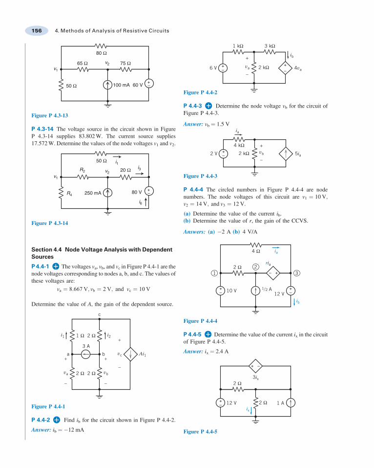
156 4. Methods of Analysis of Resistive Circuits
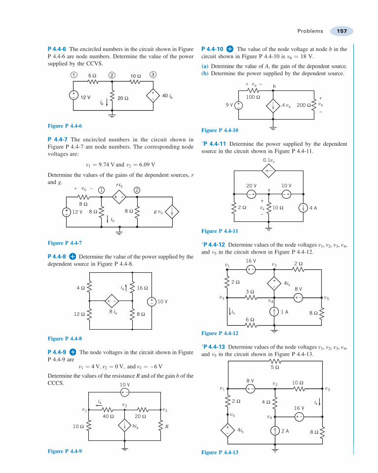
P 4.4-6 The encircled numbers in the circuit shown in FigureP 4.4-6 are node numbers. Determine the value of the powersupplied by the CCVS.
5 Ω
20 Ω12 V+–
1 2 3
+–
ia
40 ia
10 Ω
Figure P 4.4-6
P 4.4-7 The encircled numbers in the circuit shown inFigure P 4.4-7 are node numbers. The corresponding nodevoltages are:
v1 ¼ 9:74 V and v2 ¼ 6:09 V
Determine the values of the gains of the dependent sources, rand g.
+ –
+– 12 V +
+ –
–
8 Ω8 Ω 8 Ω
vb+ –
g vb
rib1 2
ib
Figure P 4.4-7
P 4.4-8 Determine the value of the power supplied by thedependent source in Figure P 4.4-8.
4 Ω
12 Ω 8 Ω
16 Ωia
8 ia
10 V+–+ –
Figure P 4.4-8
P 4.4-9 The node voltages in the circuit shown in FigureP 4.4-9 are
v1 ¼ 4 V; v2 ¼ 0 V; and v3 ¼ "6 V
Determine the values of the resistance R and of the gain b of theCCCS.
10 Ω
40 Ω 20 Ω
10 V
bia R
v1
v2ia
v3
–+
Figure P 4.4-9
P 4.4-10 The value of the node voltage at node b in thecircuit shown in Figure P 4.4-10 is vb ¼ 18 V.
(a) Determine the value of A, the gain of the dependent source.(b) Determine the power supplied by the dependent source.
100 Ω200 Ω+
–9 V
b
A va
va+ −
vb
+
−
Figure P 4.4-10
-P 4.4-11 Determine the power supplied by the dependentsource in the circuit shown in Figure P 4.4-11.
vx
+
–
+– +–
4 A
10 V20 V
10 Ω
x
2 Ω
0.1vx
Figure P 4.4-11
-P 4.4-12 Determine values of the node voltages v1, v2, v3, v4,and v5 in the circuit shown in Figure P 4.4-12.
4ix
8 Ω1 A
2 Ω
2 Ω
8 V
16 V
3 Ω
6 Ω
+ –
+ –
+–
ix
v3
v2
v4v5
v1
Figure P 4.4-12
-P 4.4-13 Determine values of the node voltages v1, v2, v3, v4,and v5 in the circuit shown in Figure P 4.4-13.
4ix 8 Ω2 A
2 Ω
10 Ω
16 V
8 V
5 Ω
4 Ω
+ –
+ –
+–
ix
v3
v2
v4
v1
v5
Figure P 4.4-13
Problems 157
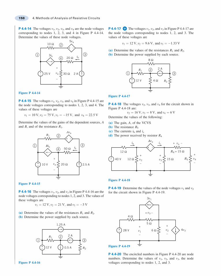
P 4.4-14 The voltages v1, v2, v3, and v4 are the node voltagescorresponding to nodes 1, 2, 3, and 4 in Figure P 4.4-14.Determine the values of these node voltages.
+ –
+–
ib3ib
5va
va
+
–
34
2
1
10 Ω
20 Ω
30 Ω25 V 2 A
Figure P 4.4-14
P 4.4-15 The voltages v1, v2, v3, and v4 in Figure P 4.4-15 arethe node voltages corresponding to nodes 1, 2, 3, and 4. Thevalues of these voltages are
v1 ¼ 10 V; v2 ¼ 75 V; v3 ¼ "15 V; and v4 ¼ 22:5 V
Determine the values of the gains of the dependent sources, Aand B, and of the resistance R1.
+ –
+–
ib
va
+
–
34
2
150 Ω
20 Ω10 V 2.5 A
Bib
R1
Ava
Figure P 4.4-15
P 4.4-16 The voltages v1, v2, and v3 in Figure P 4.4-16 are thenode voltages corresponding to nodes 1, 2, and 3. The values ofthese voltages are
v1 ¼ 12 V; v2 ¼ 21 V; and v3 ¼ "3 V
(a) Determine the values of the resistances R1 and R2.(b) Determine the power supplied by each source.
+– 12 V
R1
R2
2 A
32
1
1.25 A
0.5 A
Figure P 4.4-16
P 4.4-17 The voltages v1, v2, and v3 in Figure P 4.4-17 arethe node voltages corresponding to nodes 1, 2, and 3. Thevalues of these voltages are
v1 ¼ 12 V; v2 ¼ 9:6 V; and v3 ¼ "1:33 V
(a) Determine the values of the resistances R1 and R2.(b) Determine the power supplied by each source.
+– 12 V
R1
R2
2 A
8 Ω
32
1
4 Ω
Figure P 4.4-17
P 4.4-18 The voltages v2, v3, and v4 for the circuit shown inFigure P 4.4-18 are:
v2 ¼ 16 V; v3 ¼ 8 V; and v4 ¼ 6 VDetermine the values of the following:
(a) The gain, A, of the VCVS(b) The resistance R5
(c) The currents ib and ic(d) The power received by resistor R4
v4
+
+ –
–v3
+
–15 Ω
12 Ω
va
R5
Ava
R4 = 15 Ω
ic
v2
+
–12 Ω40 V–
+
+ –
ib
Figure P 4.4-18
P 4.4-19 Determine the values of the node voltages v1 and v2
for the circuit shown in Figure P 4.4-19.
v2
v3
4v3
+
+ –
–
4 Ω
6 Ωv1
+
–28 V–
+
5 Ω
3v1
Figure P 4.4-19
P 4.4-20 The encircled numbers in Figure P 4.4-20 are nodenumbers. Determine the values of v1, v2, and v3, the nodevoltages corresponding to nodes 1, 2, and 3.
158 4. Methods of Analysis of Resistive Circuits
– +va
10 Ω 10 V
30 Ω
–+
– +
–+
5va
10 V 2 Ω1 2 3
Figure P 4.4-20
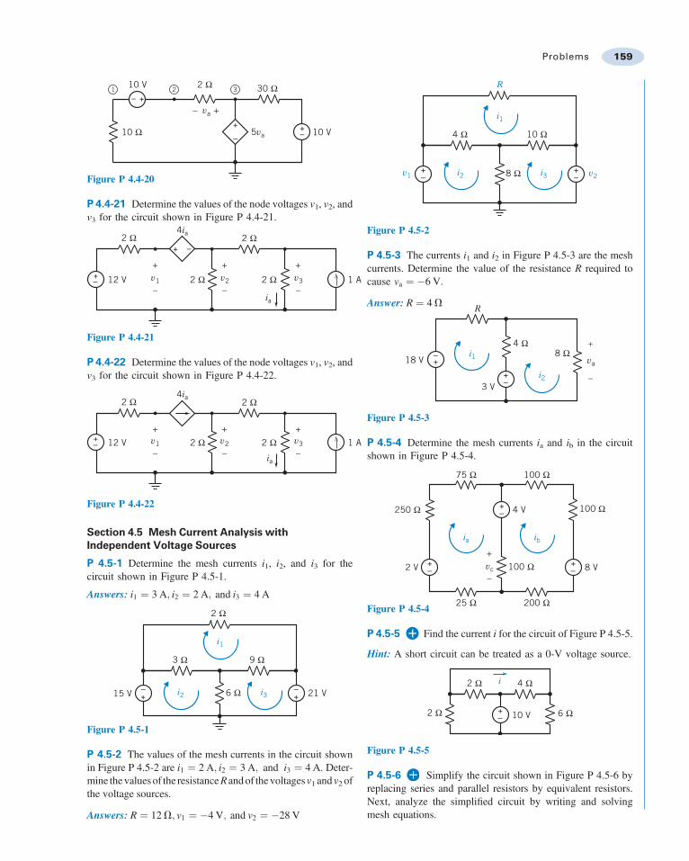
P 4.4-21 Determine the values of the node voltages v1, v2, andv3 for the circuit shown in Figure P 4.4-21.
v3
+
–v2
+
–v1
+
–
2 Ω
ia
4ia2 Ω
2 Ω2 Ω12 V 1 A–+
+ –
Figure P 4.4-21
P 4.4-22 Determine the values of the node voltages v1, v2, andv3 for the circuit shown in Figure P 4.4-22.
v3
+
–v2
+
–v1
+
–
2 Ω
ia
4ia2 Ω
2 Ω2 Ω12 V 1 A–+
Figure P 4.4-22
Section 4.5 Mesh Current Analysis withIndependent Voltage Sources
P 4.5-1 Determine the mesh currents i1, i2, and i3 for thecircuit shown in Figure P 4.5-1.
Answers: i1 ¼ 3 A; i2 ¼ 2 A; and i3 ¼ 4 A
+–
+–
3 Ω
6 Ω 15 V
9 Ω
2 Ω
21 Vi3i2
i1
Figure P 4.5-1
P 4.5-2 The values of the mesh currents in the circuit shownin Figure P 4.5-2 are i1 ¼ 2 A; i2 ¼ 3 A; and i3 ¼ 4 A. Deter-mine the values of the resistance R and of the voltages v1 and v2 ofthe voltage sources.
Answers: R ¼ 12V; v1 ¼ "4 V; and v2 ¼ "28 V
+–
+–
4 Ω
8 Ω
10 Ω
i3 v2v1 i2
i1
R
Figure P 4.5-2
P 4.5-3 The currents i1 and i2 in Figure P 4.5-3 are the meshcurrents. Determine the value of the resistance R required tocause va ¼ "6 V.
Answer: R ¼ 4V
+–
+– va
+
–
18 V
4 Ω
3 V
8 Ωi1
R
i2
Figure P 4.5-3
P 4.5-4 Determine the mesh currents ia and ib in the circuitshown in Figure P 4.5-4.
75 Ω 100 Ω
25 Ω 200 Ω
vc
+
–
+–
+–
+–
8 V2 V
4 V
100 Ω
100 Ω250 Ω
ibia
Figure P 4.5-4
P 4.5-5 Find the current i for the circuit of Figure P 4.5-5.
Hint: A short circuit can be treated as a 0-V voltage source.
2 Ω 4 Ω
2 Ω 6 Ω10 V
i
+–
Figure P 4.5-5
P 4.5-6 Simplify the circuit shown in Figure P 4.5-6 byreplacing series and parallel resistors by equivalent resistors.Next, analyze the simplified circuit by writing and solvingmesh equations.
Problems 159
(a) Determine the power supplied by each source,(b) Determine the power absorbed by the 30-V resistor.
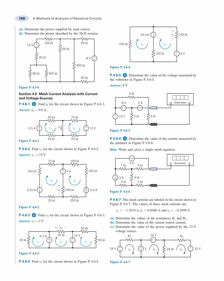
100 Ω
60 Ω
40 Ω
300 Ω
8 V
60 Ω
30 Ω
80 Ω 560 Ω
12 V +–
+–
Figure P 4.5-6
Section 4.6 Mesh Current Analysis with Currentand Voltage Sources
P 4.6-1 Find ib for the circuit shown in Figure P 4.6-1.
Answer: ib ¼ 0:6 A
75 Ω50 Ω
25 Ω50 Ω
10 V+–
ibi1 i20.5 A
Figure P 4.6-1
P 4.6-2 Find vc for the circuit shown in Figure P 4.6-2.
Answer: vc ¼ 15 V
75 Ω 100 Ω
25 Ω 200 Ω
vc
+
–
+–
0.4 A0.25 A
4 V
100 Ω
100 Ω250 Ω
ibia
Figure P 4.6-2
P 4.6-3 Find v2 for the circuit shown in Figure P 4.6-3.
Answer: v2 ¼ 2 V
20 Ω
30 Ω
60 Ω
30 Ω10 V
+–
+ –v2
i1 i2 i3
0.5 A
Figure P 4.6-3
P 4.6-4 Find vc for the circuit shown in Figure P 4.6-4.
vc
+
–
+– 9 V
20 mA
100 Ω
100 Ω
250 Ω ibia
Figure P 4.6-4
P 4.6-5 Determine the value of the voltage measured bythe voltmeter in Figure P 4.6-5.
Answer: 8 V
12 V
8 V 2 A
+–
+ –
Voltmeter
6 Ω
3 Ω5 Ω
Figure P 4.6-5
P 4.6-6 Determine the value of the current measured bythe ammeter in Figure P 4.6-6.
Hint: Write and solve a single mesh equation.
Ammeter2 A
3 A5 Ω 2 Ω
7 Ω 4 Ω
6 Ω
Figure P 4.6-6
P 4.6-7 The mesh currents are labeled in the circuit shown inFigure P 4.6-7. The values of these mesh currents are:
i1 ¼ "1:1014 A; i2 ¼ 0:8986 A and i3 ¼ "0:2899 A
(a) Determine the values of the resistances R1 and R3.(b) Determine the value of the current source current.(c) Determine the value of the power supplied by the 12-V
voltage source.
+– i1 i2Is 24 Ω
R1 R3
i3+–
+ –12 V
32 V24 V
Figure P 4.6-7
160 4. Methods of Analysis of Resistive Circuits
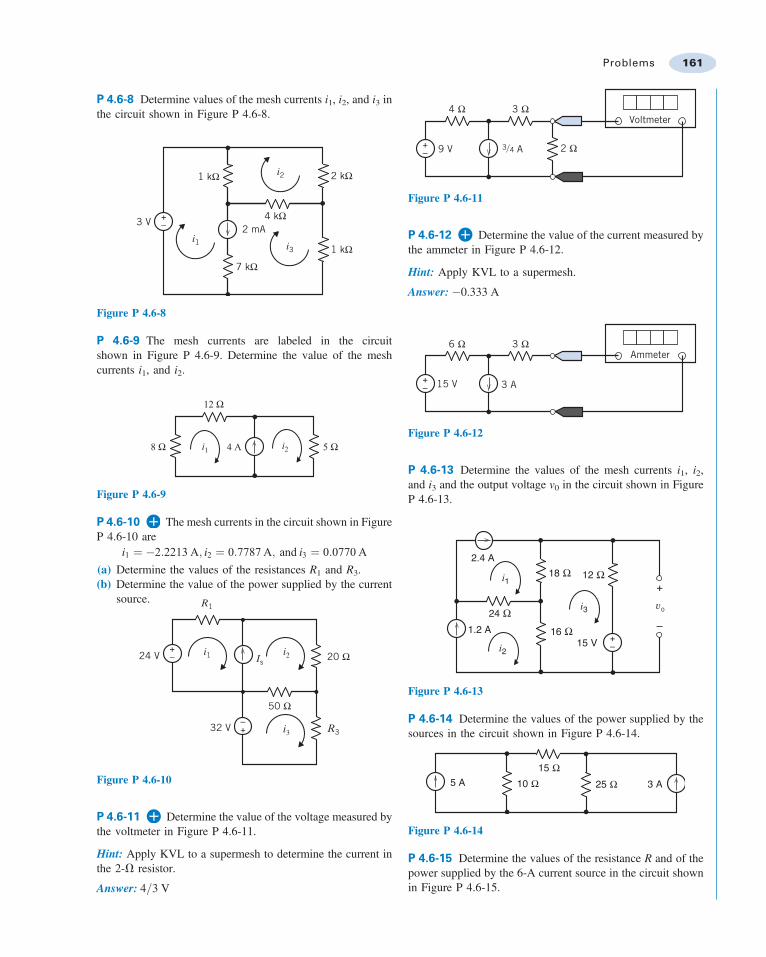
P 4.6-8 Determine values of the mesh currents i1, i2, and i3 inthe circuit shown in Figure P 4.6-8.
1 kΩ
4 kΩ
2 kΩ
1 kΩ
7 kΩ
2 mA3 V +
–i1
i2
i3
Figure P 4.6-8
P 4.6-9 The mesh currents are labeled in the circuitshown in Figure P 4.6-9. Determine the value of the meshcurrents i1, and i2.
4 A
12 Ω
8 Ω 5 Ωi2i1
Figure P 4.6-9
P 4.6-10 The mesh currents in the circuit shown in FigureP 4.6-10 are
i1 ¼ "2:2213 A; i2 ¼ 0:7787 A; and i3 ¼ 0:0770 A
(a) Determine the values of the resistances R1 and R3.(b) Determine the value of the power supplied by the current
source.
24 V
32 V
Is
R1
R3
20 Ω
50 Ω
i2i1
i3
+–
+–
Figure P 4.6-10
P 4.6-11 Determine the value of the voltage measured bythe voltmeter in Figure P 4.6-11.
Hint: Apply KVL to a supermesh to determine the current inthe 2-V resistor.
Answer: 4=3 V
A9 V+– 2 Ω
4 Ω 3 ΩVoltmeter
3 4
Figure P 4.6-11
P 4.6-12 Determine the value of the current measured bythe ammeter in Figure P 4.6-12.
Hint: Apply KVL to a supermesh.
Answer: "0.333 A
3 A15 V+–
6 Ω 3 ΩAmmeter
Figure P 4.6-12
P 4.6-13 Determine the values of the mesh currents i1, i2,and i3 and the output voltage v0 in the circuit shown in FigureP 4.6-13.
i1
24 Ω
+–15 V
2.4 A
i2
i3
1.2 A
18 Ω
16 Ω
12 Ω+
–
vo
Figure P 4.6-13
P 4.6-14 Determine the values of the power supplied by thesources in the circuit shown in Figure P 4.6-14.
25 Ω 3 A5 A15 Ω
10 Ω
Figure P 4.6-14
P 4.6-15 Determine the values of the resistance R and of thepower supplied by the 6-A current source in the circuit shownin Figure P 4.6-15.
Problems 161
2.5 A
1 A
6 A5 Ω
5 Ω
10 Ω
4 Ω
R
Figure P 4.6-15
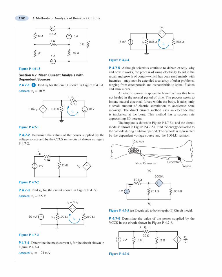
Section 4.7 Mesh Current Analysis withDependent Sources
P 4.7-1 Find v2 for the circuit shown in Figure P 4.7-1.
Answer: v2 ¼ 10 V
v2+ –
50 Ω
100 Ω 10 V0.04v2+–i1
Figure P 4.7-1
P 4.7-2 Determine the values of the power supplied by thevoltage source and by the CCCS in the circuit shown in FigureP 4.7-2.
2 kΩ2 V
4 kΩ
ia
5ia+–
Figure P 4.7-2
P 4.7-3 Find vo for the circuit shown in Figure P 4.7-3.
Answer: vo ¼ 2.5 V
60 mA 100 Ω 250 Ω
vo = 50ib
ib ia
+ –
Figure P 4.7-3
P 4.7-4 Determine the mesh current ia for the circuit shown inFigure P 4.7-4.
Answer: ia ¼ "24 mA
vb
+
–6 mA 100 Ω 250 Ω
3vb
ia
+ –
Figure P 4.7-4
P 4.7-5 Although scientists continue to debate exactly whyand how it works, the process of using electricity to aid in therepair and growth of bones—which has been used mainly withfractures—may soon be extended to an array of other problems,ranging from osteoporosis and osteoarthritis to spinal fusionsand skin ulcers.
An electric current is applied to bone fractures that havenot healed in the normal period of time. The process seeks toimitate natural electrical forces within the body. It takes onlya small amount of electric stimulation to accelerate bonerecovery. The direct current method uses an electrode thatis implanted at the bone. This method has a success rateapproaching 80 percent.
The implant is shown in Figure P 4.7-5a, and the circuitmodel is shown in Figure P 4.7-5b. Find the energy delivered tothe cathode during a 24-hour period. The cathode is representedby the dependent voltage source and the 100-kV resistor.
3 V 20 kΩ 100 kΩ
10 kΩ
Micro Connector
5000i1
i1
+ –
+–
(b)
(a)
GeneratorAnode
Cathode
Figure P 4.7-5 (a) Electric aid to bone repair. (b) Circuit model.
P 4.7-6 Determine the value of the power supplied by theVCCS in the circuit shown in Figure P 4.7-6.
2 Ω2 A20 Ω
8 Ω
+ –va
va
2
Figure P 4.7-6
162 4. Methods of Analysis of Resistive Circuits
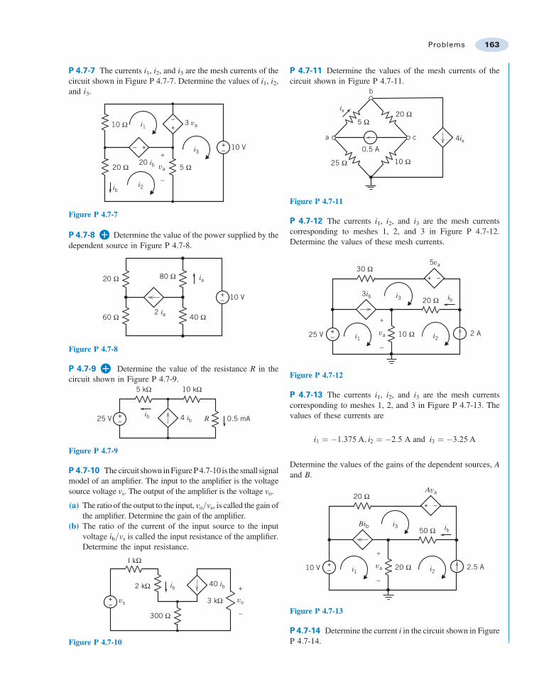
P 4.7-7 The currents i1, i2, and i3 are the mesh currents of thecircuit shown in Figure P 4.7-7. Determine the values of i1, i2,and i3.
10 V
5 Ω20 Ω
10 Ω 3 va
20 ib
ib
+
−
va
i3
i2
i1
+–+–
+–
Figure P 4.7-7
P 4.7-8 Determine the value of the power supplied by thedependent source in Figure P 4.7-8.
10 V
40 Ω
80 Ω20 Ω
60 Ω2 ia
ia
+–
Figure P 4.7-8
P 4.7-9 Determine the value of the resistance R in thecircuit shown in Figure P 4.7-9.
0.5 mA25 V
5 kΩ 10 kΩ
4 ibib R+
–
Figure P 4.7-9
P 4.7-10 The circuit shown in Figure P 4.7-10 is the small signalmodel of an amplifier. The input to the amplifier is the voltagesource voltage vs. The output of the amplifier is the voltage vo.
(a) The ratio of the output to the input, vo=vs, is called the gain ofthe amplifier. Determine the gain of the amplifier.
(b) The ratio of the current of the input source to the inputvoltage ib=vs is called the input resistance of the amplifier.Determine the input resistance.
1 kΩ
2 kΩ
3 kΩ
300 Ω
40 ibib
vs
+
−
vo+–
Figure P 4.7-10
P 4.7-11 Determine the values of the mesh currents of thecircuit shown in Figure P 4.7-11.
4ix
ix
b
a c
0.5 A
5 Ω
10 Ω25 Ω
20 Ω
Figure P 4.7-11
P 4.7-12 The currents i1, i2, and i3 are the mesh currentscorresponding to meshes 1, 2, and 3 in Figure P 4.7-12.Determine the values of these mesh currents.
+ –
+–
ib3ib
5va
va
+
–
30 Ω
20 Ω
10 Ω25 V 2 Ai2i1
i3
Figure P 4.7-12
P 4.7-13 The currents i1, i2, and i3 are the mesh currentscorresponding to meshes 1, 2, and 3 in Figure P 4.7-13. Thevalues of these currents are
i1 ¼ "1:375 A; i2 ¼ "2:5 A and i3 ¼ "3:25 A
Determine the values of the gains of the dependent sources, Aand B.
+ –
+–
ib
va
+
–
20 Ω
50 Ω
20 Ω10 V 2.5 Ai2i1
i3
Ava
Bib
Figure P 4.7-13
P 4.7-14 Determine the current i in the circuit shown in FigureP 4.7-14.
Problems 163
Answer: i ¼ 3 A
12 A 28 Ω
4 Ω
2i
8 Ωi
Figure P 4.7-14
P 4.7-15 Determine the values of the mesh currents i1 and i2for the circuit shown in Figure P 4.7-15.
2 Ω
ia
4ia2 Ω
2 Ω2 Ω12 V 1 A–+ i2i1
Figure P 4.7-15
P 4.7-16 Determine the values of the mesh currents i1 and i2for the circuit shown in Figure P 4.7-16.
2 Ω
ia
4ia2 Ω
2 Ω2 Ω12 V 1 A–+ i2i1
+ –
Figure P 4.7-16
Section 4.8 The Node Voltage Method and MeshCurrent Method Compared
P 4.8-1 The circuit shown in Figure P 4.8-1 has two inputs, vs
and is, and one output, vo. The output is related to the inputs bythe equation
vo ¼ ais þ bvs
where a and b are constants to be determined. Determine thevalues a and b by (a) writing and solving mesh equations and(b) writing and solving node equations.
vs
is
120 Ω 30 Ω
32 Ω96 Ω
+
−vo
+ –
Figure P 4.8-1
P 4.8-2 Determine the power supplied by the dependentsource in the circuit shown in Figure P 4.8-2 by writing andsolving (a) node equations and (b) mesh equations.
120 V
ia = 0.2 va
50 Ω 10 Ω
+ −va
+ –
Figure P 4.8-2
Section 4.9 Circuit Analysis Using MATLAB
P 4.9-1 The encircled numbers in the circuit shown FigureP 4.9-1 are node numbers. Determine the values of the corre-sponding node voltages v1, v2, and v3.
3 A
4 Ω1 25 Ω
2 Ω
3
10 Ω5 A
Figure P 4.9-1
P 4.9-2 Determine the values of the node voltages v1 and v2 inthe circuit shown in Figure P 4.9-2.
8 V
40 Ω50 Ω
20 Ω
10 Ω15 V
v2
+–+
–
25 Ω
v1
Figure P 4.9-2
P 4.9-3 Determine the values of the node voltages v1, v2, andv3 in the circuit shown in Figure P 4.9-3.
10 V
40 Ω20 Ω
50 Ω
25 Ω15 V
v2
+–+
–
25 Ω
v1
10 Ω
v3
Figure P 4.9-3
164 4. Methods of Analysis of Resistive Circuits
P 4.9-4 Determine the node voltages v1 and v2 for the circuitshown in Figure P 4.9-4.
v1
+
–
v2
+
–
+–
25 Ω 14 Ω
8 Ω 9 Ω
2 A
24 V
Figure P 4.9-4
P 4.9-5 Determine the mesh currents i1 and i2 for the circuitshown in Figure P 4.9-5.
+–
25 Ω 14 Ω
8 Ω 9 Ω
2 A
24 Vi1 i2
Figure P 4.9-5
P 4.9-6 Represent the circuit shown in Figure P 4.9-6 by thematrix equation
a 11 a 12
a 21 a 22
% &v 1
v 2
% &¼ "40
"228
% &
Determine the values of the coefficients a11, a12, a21, and a22.
v1
+
–
v2
+
–
+–
10 Ω
22 Ω
10 Ω 19 Ω
0.4 A
10 V
Figure P 4.9-6
P 4.9-7 Represent the circuit shown in Figure P 4.9-7 by thematrix equation
a 11 a 12
a 21 a 22
% &i 1i 2
% &¼ 4
10
% &
Determine the values of the coefficients a11, a12, a21, and a22.
+–
10 Ω
22 Ω
10 Ω 19 Ω
0.4 A
10 V
i1 i2
Figure P 4.9-7
P 4.9-8 Determine the values of the power supplied by each ofthe sources for the circuit shown in Figure P 4.9-8.
40 Ω
24 V +–2.4 A40 Ω
5 Ω 5 Ω
Figure P 4.9-8
P 4.9-9 The mesh currents are labeled in the circuit shownin Figure P 4.9-9. Determine the value of the mesh currents i1and i2.
8 Ω i24 Ω
8 Ω+–i1
4 Ω
+ –
6 V
+ –
15 V
4 Ω
5 i1
i1
Figure P 4.9-9
P 4.9-10 The encircled numbers in the circuit shown in FigureP 4.9-10 are node numbers. Determine the values of thecorresponding node voltages v1 and v2.
10 Ω 4 Ω2.5 A
2 Ω
1.5 v1v1
+
–
10 Ω5 A
1 2
Figure P 4.9-10
Problems 165
Section 4.11 How CanWe Check . . . ?
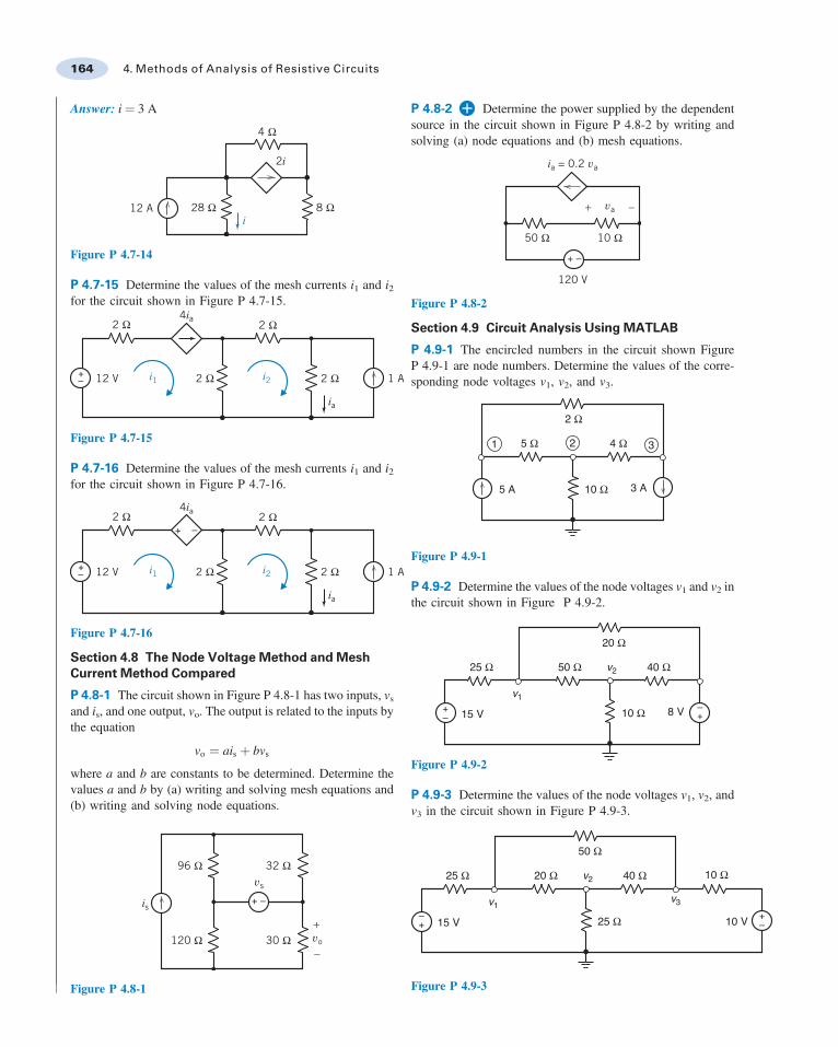
P 4.11-1 Computer analysis of the circuit shown in FigureP 4.11-1 indicates that the node voltages are va ¼ 5:2 V;vb ¼ "4:8 V; and vc ¼ 3:0 V. Is this analysis correct?
Hint: Use the node voltages to calculate all the elementcurrents. Check to see that KCL is satisfied at each node.
10 V
A
a
3 Ω2 Ω
4 Ω 5 Ω
+ –
bc
1 2
Figure P 4.11-1
P 4.11-2 An old lab report asserts that the node voltages ofthe circuit of Figure P 4.11-2 are va ¼ 4 V; vb ¼ 20 V;and vc ¼ 12 V. Are these correct?
2 Ω2 Ω
4 Ω2 Ω
2ix
ix
b
a c
2 A
Figure P 4.11-2
P 4.11-3 Your lab partner forgot to record the values of R1,R2, and R3. He thinks that two of the resistors in FigureP 4.11-3 had values of 10 kV and that the other had avalue of 5 kV. Is this possible? Which resistor is the 5-kVresistor?
7 . 5 0
R1 R2
R312 V 6 V+–
+–
Voltmeter
Figure P 4.11-3
P 4.11-4 Computer analysis of the circuit shown in FigureP 4.11-4 indicates that the mesh currents are i1 ¼ 2 A;i2 ¼ 4 A, and i3 ¼ 3 A. Verify that this analysis is correct.
Hint: Use the mesh currents to calculate the element voltages.Verify that KVL is satisfied for each mesh.
+– +
–
10 Ω
8 Ω
4 Ω
12 Ω
i3i2
i1
4 V28 V
Figure P 4.11-4
166 4. Methods of Analysis of Resistive Circuits
PSpice ProblemsSP 4-1 Use PSpice to determine the node voltages of thecircuit shown in Figure SP 4-1.
4 i1
i1
a
2 Ω 2 Ω
1 Ω 2 Ω
3 A
b
c
Figure SP 4-1
SP 4-2 Use PSpice to determine the mesh currents of thecircuit shown in Figure SP 4-2 when R ¼ 4 V.
va
+
–3 V
18 V
4 Ω
8 Ω
i2i1
+–
+–
R
Figure SP 4-2
SP 4-3 The voltages va, vb, vc, and vd in Figure SP 4-3 are thenode voltages corresponding to nodes a, b, c, and d. Thecurrent i is the current in a short circuit connected betweennodes b and c. Use PSpice to determine the values of va, vb, vc,and vd and of i.
vd
+
–vc
+
–4 k Ω
4 k Ω
1 mA
8 Vi
vb
+
–va
+
–2 mA12 V+
–
+ –a b c d
Figure SP 4-3
SP 4-4 Determine the current i shown in Figure SP 4-4.
Answer: i ¼ 0.56 A
1 Ω2 Ω
1 Ω 1 Ω
3 Ω
3 Ω 2 Ω
2 Ω
+–
+–
4 V
4 V
i
Figure SP 4-4
Design ProblemsDP 4-1 An electronic instrument incorporates a 15-V powersupply. A digital display is added that requires a 5-V powersupply. Unfortunately, the project is over budget, and you areinstructed to use the existing power supply. Using a voltagedivider, as shown in Figure DP 4-1, you are able to obtain 5 V.The specification sheet for the digital display shows that thedisplay will operate properly over a supply voltage range of 4.8 Vto 5.4 V. Furthermore, the display will draw 300 mA (I) when thedisplay is active and 100 mA when quiescent (no activity).
(a) Select values of R1 and R2 so that the display will be suppliedwith 4.8 V to 5.4 V under all conditions of current I.
(b) Calculate the maximum power dissipated by each resistor, R1
and R2, and the maximum current drawn from the 15-V supply.(c) Is the use of the voltage divider a good engineering solution?
If not, why? What problems might arise?
15-voltpowersupply
Digitaldisplay
R1
I
R2
+
–
Figure DP 4-1
DP 4-2 For the circuit shown in Figure DP 4-2, it is desired toset the voltage at node a equal to 0 V control an electric motor.Select voltages v1 and v2 to achieve va ¼ 0 V when v1 and v2 areless than 20 V and greater than zero and R ¼ 2 V.
Design Problems 167
v2+–
a
+–
R
v1
R R
+–
8 V R
R
Figure DP 4-2
DP 4-3 A wiring circuit for a special lamp in a home is shown inFigure DP 4-3. The lamp has a resistance of 2V, and the designerselects R ¼ 100 V. The lamp will light when I . 50 mA but willburn out when I > 75 mA.
(a) Determine the current in the lamp and whether it will lightfor R ¼ 100V.
(b) Select R so that the lamp will light but will not burn out if Rchanges by /10 percent because of temperature changes inthe home.
5 V +– I 2 Ω300 Ω
50 Ω R
Lamp
Figure DP 4-3 A lamp circuit.
D P 4-4 To control a device using the circuit shown in FigureDP 4-4, it is necessary that vab ¼ 10 V. Select the resistors whenit is required that all resistors be greater than 1 V andR3 þ R4 ¼ 20 V.
R2+–25 V R4
R3
5 Ω
10 Ω
R1
a
b
Figure DP 4-4
DP 4-5 The current i shown in the circuit of Figure DP 4-5 isused to measure the stress between two sides of an earth faultline. Voltage v1 is obtained from one side of the fault, and v2 isobtained from the other side of the fault. Select the resistancesR1, R2, and R3 so that the magnitude of the current i will remainin the range between 0.5 mA and 2 mA when v1 and v2 may eachvary independently between þ1 V and þ2 V 1 V 0 vn 0 2 Vð Þ.
v1+–
i
R3 v2+–
R2R1
Figure DP 4-5 A circuit for earth fault-line stress measurement.