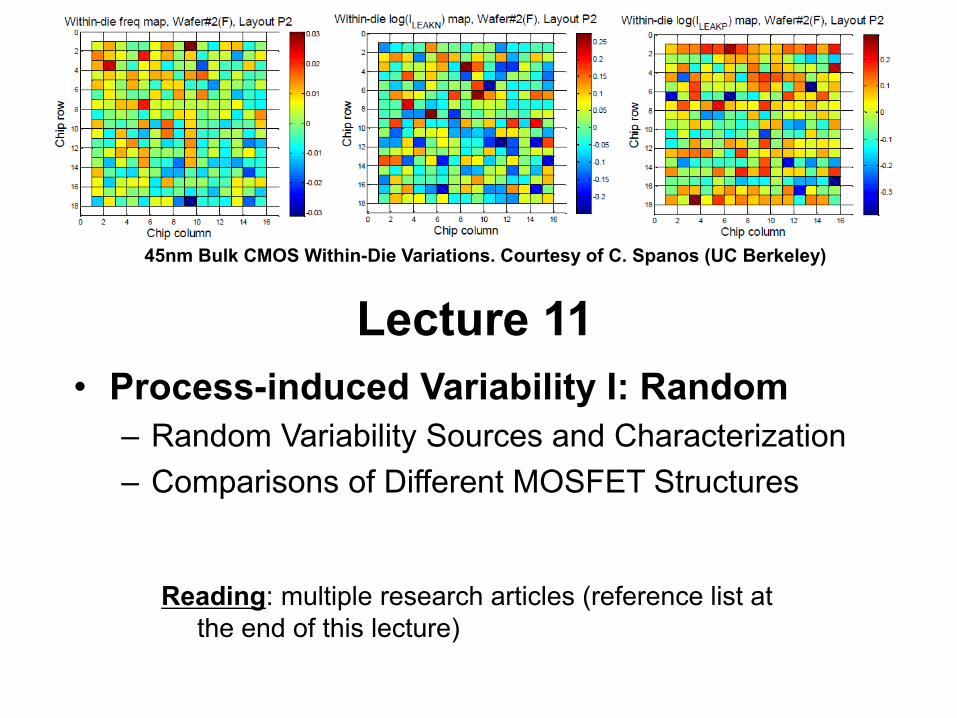
Lecture 11 • Process-induced Variability I: Random – Random Variability Sources and Characterization – Comparisons of Different MOSFET Structures Reading: multiple research articles (reference list at the end of this lecture) 45nm Bulk CMOS Within-Die Variations. Courtesy of C. Spanos (UC Berkeley)
Transcript
Lecture 11
• Process-induced Variability I: Random
– Random Variability Sources and Characterization
– Comparisons of Different MOSFET Structures
Reading: multiple research articles (reference list at
the end of this lecture)
45nm Bulk CMOS Within-Die Variations. Courtesy of C. Spanos (UC Berkeley)
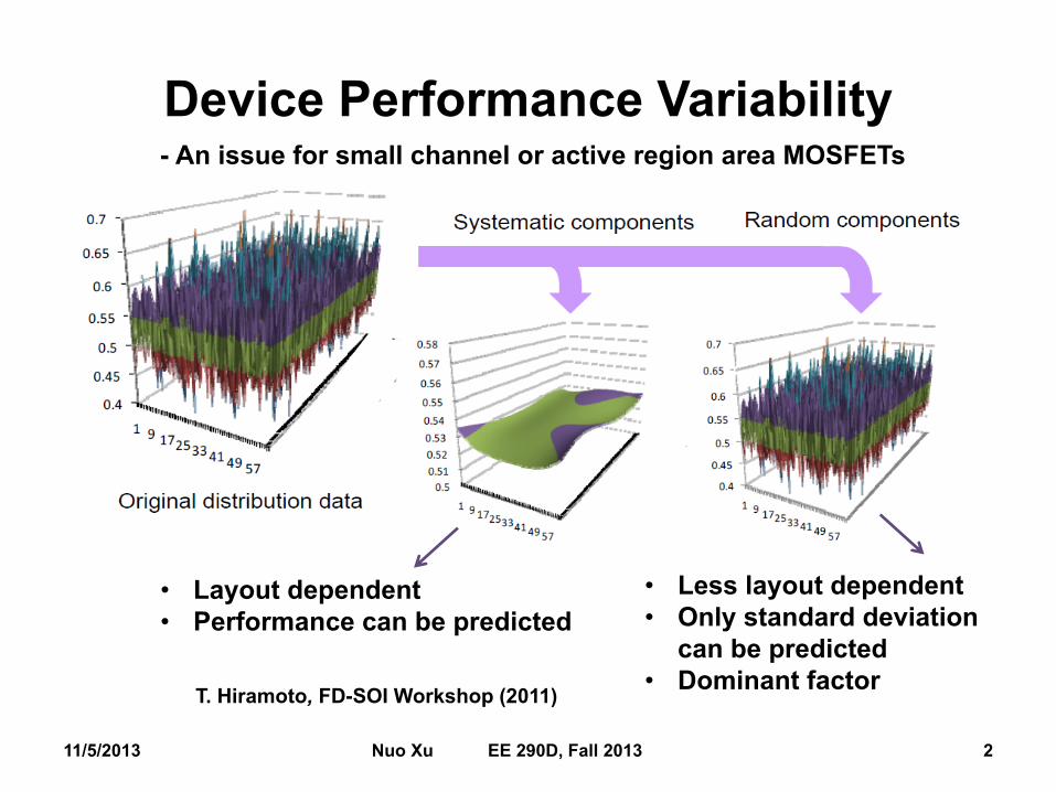
Device Performance Variability
11/5/2013 2 Nuo Xu EE 290D, Fall 2013
• Layout dependent
• Performance can be predicted
• Less layout dependent
• Only standard deviation
can be predicted
• Dominant factor
- An issue for small channel or active region area MOSFETs
T. Hiramoto, FD-SOI Workshop (2011)
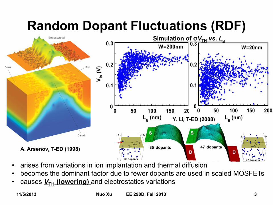
Random Dopant Fluctuations (RDF)
11/5/2013 3 Nuo Xu EE 290D, Fall 2013
• arises from variations in ion implantation and thermal diffusion
• becomes the dominant factor due to fewer dopants are used in scaled MOSFETs
• causes VTH (lowering) and electrostatics variations
A. Arsenov, T-ED (1998)
Simulation of σVTH vs. Lg
Y. Li, T-ED (2008)
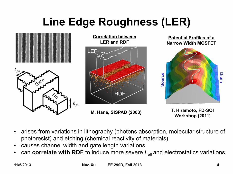
Line Edge Roughness (LER)
11/5/2013 4 Nuo Xu EE 290D, Fall 2013
Potential Profiles of a
Narrow Width MOSFET
Correlation between
LER and RDF
T. Hiramoto, FD-SOI
Workshop (2011)
• arises from variations in lithography (photons absorption, molecular structure of
photoresist) and etching (chemical reactivity of materials)
• causes channel width and gate length variations
• can correlate with RDF to induce more severe Leff and electrostatics variations
M. Hane, SISPAD (2003)
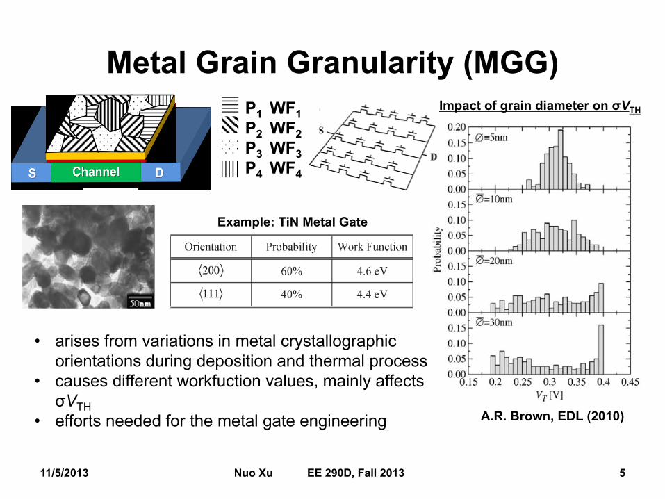
Metal Grain Granularity (MGG)
11/5/2013 5 Nuo Xu EE 290D, Fall 2013
• arises from variations in metal crystallographic
orientations during deposition and thermal process
• causes different workfuction values, mainly affects
σVTH
• efforts needed for the metal gate engineering
Impact of grain diameter on σVTH
A.R. Brown, EDL (2010)
Example: TiN Metal Gate
P1
P2
P3
P4
WF1
WF2
WF3
WF4
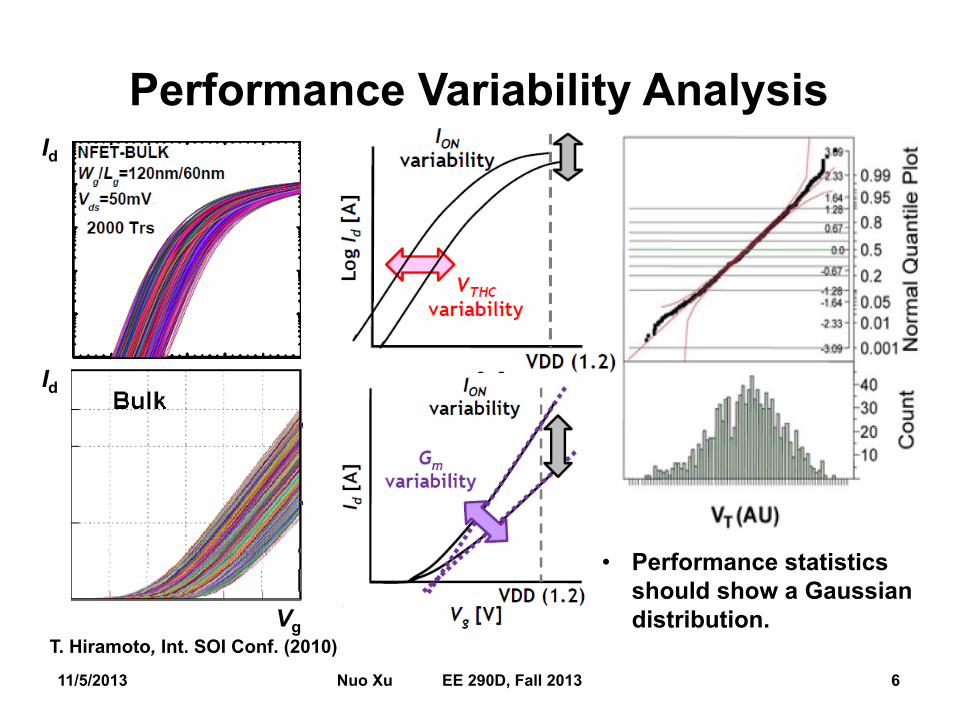
Performance Variability Analysis
11/5/2013 6 Nuo Xu EE 290D, Fall 2013
T. Hiramoto, Int. SOI Conf. (2010)
• Performance statistics
should show a Gaussian
distribution.
Id
Id
Vg
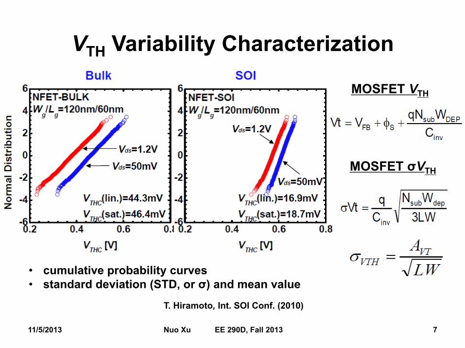
VTH Variability Characterization
11/5/2013 7 Nuo Xu EE 290D, Fall 2013
• cumulative probability curves
• standard deviation (STD, or σ) and mean value
T. Hiramoto, Int. SOI Conf. (2010)
MOSFET VTH
MOSFET σVTH
Pelgrom Plot
11/5/2013 8 Nuo Xu EE 290D, Fall 2013
• Pelgrom plot cannot unify the
MOSFET σVTH with different Nsub
and tOX
needs a better, universal model! M. J. Pelgrom, JSSC (1989)
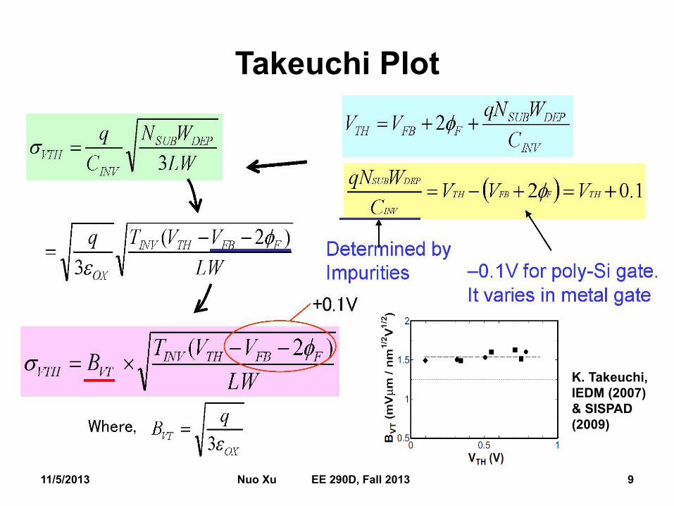
Takeuchi Plot
11/5/2013 9 Nuo Xu EE 290D, Fall 2013
K. Takeuchi,
IEDM (2007)
& SISPAD
(2009)
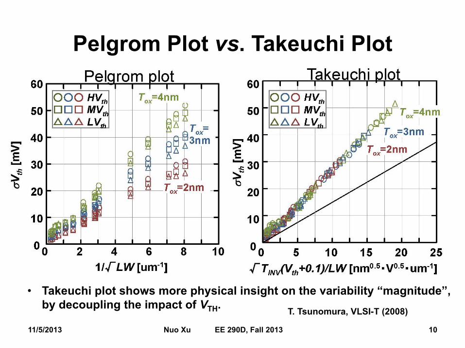
Pelgrom Plot vs. Takeuchi Plot
11/5/2013 10 Nuo Xu EE 290D, Fall 2013
• Takeuchi plot shows more physical insight on the variability “magnitude”,
by decoupling the impact of VTH. T. Tsunomura, VLSI-T (2008)
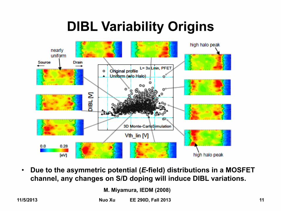
DIBL Variability Origins
11/5/2013 11 Nuo Xu EE 290D, Fall 2013
M. Miyamura, IEDM (2008)
• Due to the asymmetric potential (E-field) distributions in a MOSFET
channel, any changes on S/D doping will induce DIBL variations.
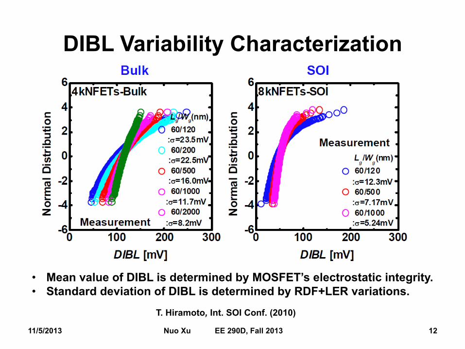
DIBL Variability Characterization
11/5/2013 12 Nuo Xu EE 290D, Fall 2013
• Mean value of DIBL is determined by MOSFET’s electrostatic integrity.
• Standard deviation of DIBL is determined by RDF+LER variations.
T. Hiramoto, Int. SOI Conf. (2010)
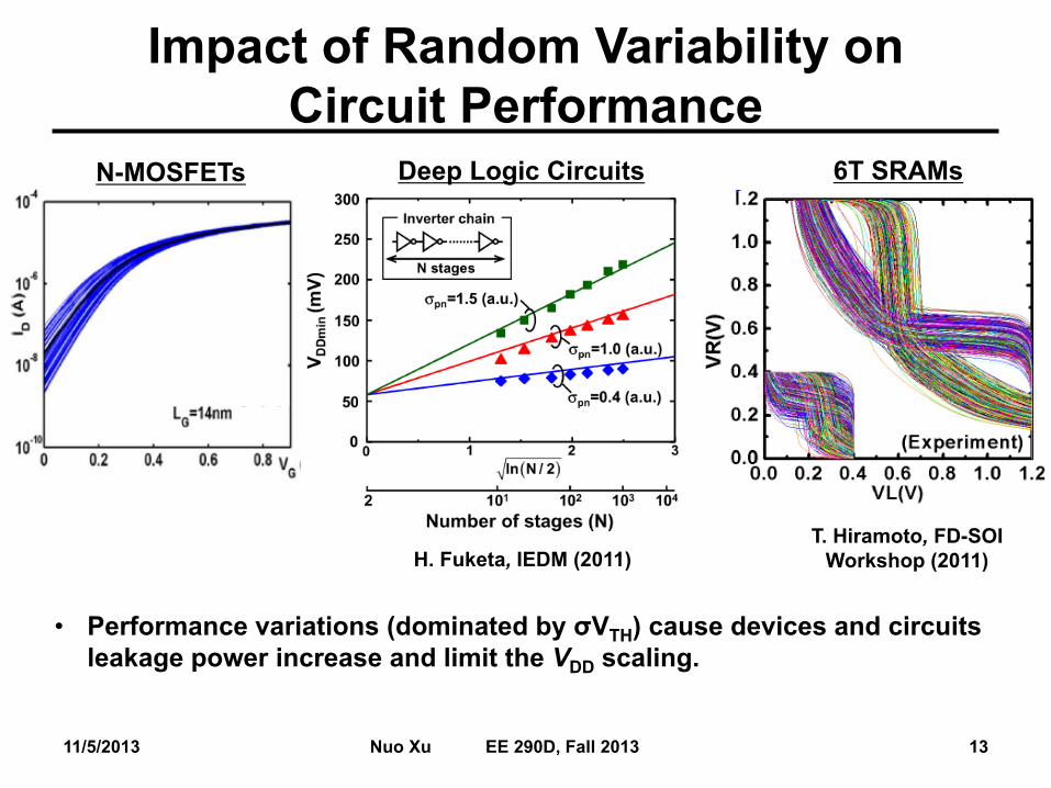
Impact of Random Variability on
Circuit Performance
11/5/2013 13 Nuo Xu EE 290D, Fall 2013
• Performance variations (dominated by σVTH) cause devices and circuits
leakage power increase and limit the VDD scaling.
H. Fuketa, IEDM (2011) T. Hiramoto, FD-SOI
Workshop (2011)
Deep Logic Circuits 6T SRAMs N-MOSFETs
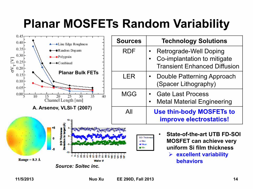
Planar MOSFETs Random Variability
11/5/2013 14 Nuo Xu EE 290D, Fall 2013
Sources Technology Solutions
RDF • Retrograde-Well Doping
• Co-implantation to mitigate
Transient Enhanced Diffusion
LER • Double Patterning Approach
(Spacer Lithography)
MGG • Gate Last Process
• Metal Material Engineering
All Use thin-body MOSFETs to
improve electrostatics!
Source: Soitec inc.
A. Arsenov, VLSI-T (2007)
• State-of-the-art UTB FD-SOI
MOSFET can achieve very
uniform Si film thickness
excellent variability
behaviors
Planar Bulk FETs
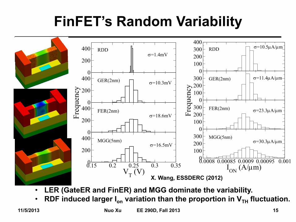
FinFET’s Random Variability
0
200
400
0
200
400
0
200
400
Fre
qu
ency
0.15 0.2 0.25 0.3 0.35V
T (V)
0
200
400
RDD
GER(2nm)
FER(2nm)
MGG(5nm)
s=1.4mV
s=10.3mV
s=18.6mV
s=16.5mV
0
100
200
300
400
0
100
200
300
0
100
200
300
Fre
qu
ency
0.0008 0.00085 0.0009 0.00095 0.001ION
(A/mm)
0
100
200
300
RDD
GER(2nm)
FER(2nm)
MGG(5nm)
s=23.3mA/mm
s=11.4mA/mm
s=10.5mA/mm
s=30.3mA/mm
• LER (GateER and FinER) and MGG dominate the variability.
• RDF induced larger Ion variation than the proportion in VTH fluctuation.
11/5/2013 15 Nuo Xu EE 290D, Fall 2013
w/ RDF
w/ MGG
w/ LER
X. Wang, ESSDERC (2012)
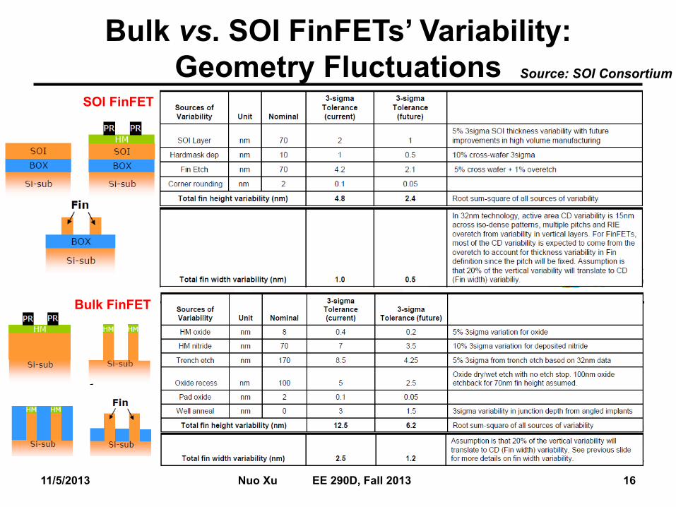
Bulk vs. SOI FinFETs’ Variability:
Geometry Fluctuations
11/5/2013 16 Nuo Xu EE 290D, Fall 2013
Bulk FinFET
SOI FinFET
Source: SOI Consortium
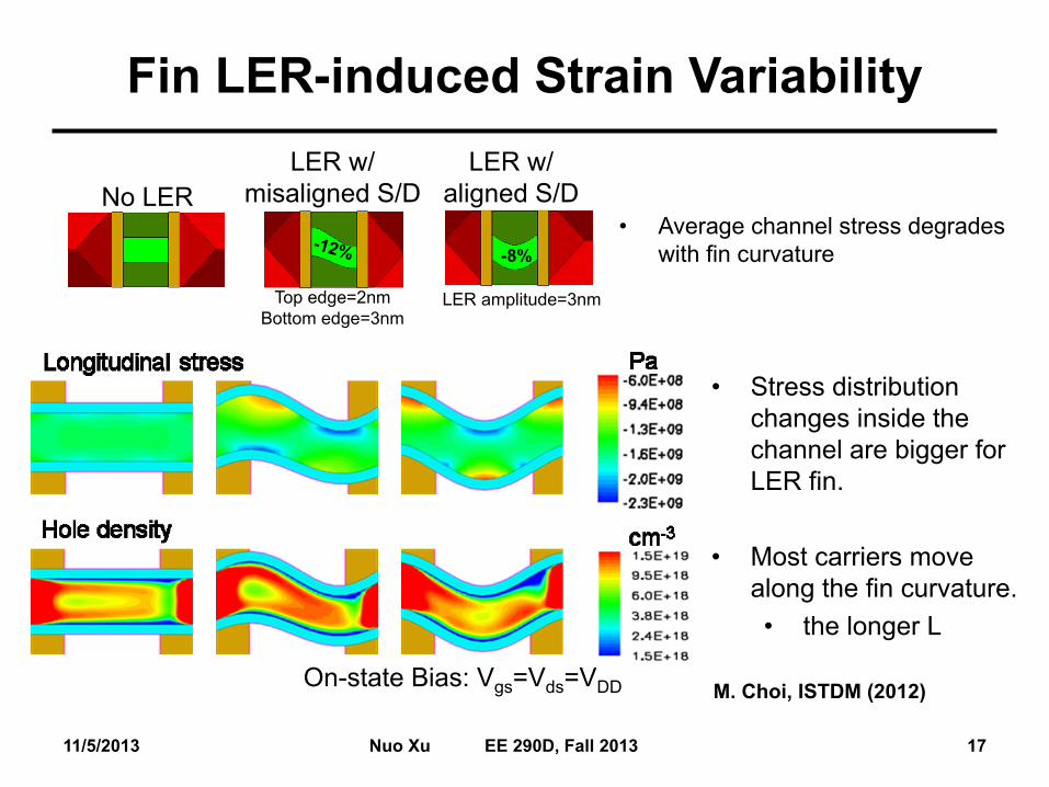
Fin LER-induced Strain Variability
11/5/2013 17 Nuo Xu EE 290D, Fall 2013
• Average channel stress degrades
with fin curvature -8%
LER amplitude=3nm
No LER
LER w/
misaligned S/D
Top edge=2nm
Bottom edge=3nm
• Stress distribution
changes inside the
channel are bigger for
LER fin.
• Most carriers move
along the fin curvature.
• the longer L
On-state Bias: Vgs=Vds=VDD
LER w/
aligned S/D
M. Choi, ISTDM (2012)
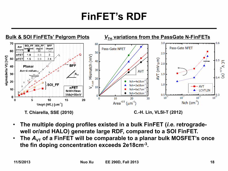
FinFET’s RDF
11/5/2013 18 Nuo Xu EE 290D, Fall 2013
T. Chiarella, SSE (2010) C.-H. Lin, VLSI-T (2012)
• The multiple doping profiles existed in a bulk FinFET (i.e. retrograde-
well or/and HALO) generate large RDF, compared to a SOI FinFET.
• The AVT of a FinFET will be comparable to a planar bulk MOSFET’s once
the fin doping concentration exceeds 2e18cm-3.
Bulk & SOI FinFETs’ Pelgrom Plots VTH variations from the PassGate N-FinFETs
References 1. T. Hiramoto, “Device Variability Benchmark for Bulk and FDSOI MOSFETs,” FD-SOI Workshop,
Taiwan, 2011.
2. A. Arsenov, “Random Dopant Induced Threshold Voltage Lowering and Fluctuations in Sub-0.1um
MOSFET's A 3D “Atomistic” Simulation Study,” IEEE Transactions on Electron Devices, vol.45,
no.12, pp. 2505-2513, 1998.
3. Y. Li et al., “Discrete Dopant Fluctuations in 20-nm/15-nm Gate Planar CMOS,” IEEE Transactions
on Electron Devices, vol.55, no.6, pp.1449-1455, 2008.
4. M. Hane et al., “Coupled Atomistic 3D Process/Device Simulation Considering Both Line-Edge
Roughness and Random-Discrete-Dopant Effects,” SISPAD, pp.99-102, 2003.
5. A.R. Brown et al., “Impact of Metal Gate Granularity on Threshold Voltage Variability A Full-Scale
Three-Dimensional Statistical Simulation Study,” IEEE Electron Device Letters, vol.31, no.11,
pp.1199-1201, 2010.
6. H. Fuketa et al., “Device Circuit Interactions in Extremely Low Voltage CMOS Designs,” IEEE
International Electron Devices Meeting Tech. Dig., pp. 559-562, 2011.
7. M.J.M. Pelgrom et al., “Matching properties of MOS transistors,” IEEE Journal of Solid-State
Circuits, vol.24, pp.1433-1439, 1989.
8. K. Takeuchi et al., “Understanding random threshold voltage fluctuation by comparing multiple
fabs and technologies,” IEEE International Electron Devices Meeting Tech. Dig., pp. 467-470,
2007.
9. K. Takeuchi et al., “Random Fluctuations in Scaled MOS Devices,” SISPAD, pp.79-85, 2009.
10. M. Miyamura et al., “Effects of Drain Bias on Threshold Voltage Fluctuation and its Impact on
Circuit Characteristics,” IEEE International Electron Devices Meeting Tech. Dig., pp. 447-450,
2008.
11. T. Tsunomura et al., “Analysis of 5σ Vth Fluctuation in 65nm-MOSFETs Using Takeuchi Plot,”
Symp. VLSI Tech., Dig., pp.156-157, 2008.
References 12. M. Choi et al., “14nm FinFET Stress Engineering with Epitaxial SiGe Source/Drain,” International
SiGe Technology and Device Meeting, Berkeley, CA, 2012.
13. A, Arsenov et al., “Simulation of Statistical Variability in Nano MOSFETs,” Symp. VLSI Technology
Dig., pp.86-87, 2007.
14. X. Wang et al., “Statistical Variability in 14nm Node SOI FinFETs and its Impact on Corresponding
6T-SRAM Cell Design,” ESSDERC, pp. 113-116, 2012.
15. C.-H. Lin et al., “Channel Doping Impact on FinFETs for 22nm and Beyond,” Symp. VLSI
Technology Dig., pp.15-16, 2012.
16. T. Chiarella et al., “Benchmarking SOI and Bulk FinFET Alternatives for Planar CMOS Scaling