4.5V to 18V, 5A 1ch Synchronous Buck Converter BD86120EFJ
Description
The BD86120EFJ is synchronous buck converters. The
device integrates power MOSFETS that provide a each
maximums current output current continuous load current
over a wide operating input voltage of 4.5V to 18V.
Current mode operation provides fast transient response
and easy phase compensation.
The output power MOSFETs using P-type MOSEFT (HI
side) and N-type MOSEFT (LOW side), then this device
don’t need boot capacitor.
The BD86120EFJ is HTSOP-J8 standard packages.
Applications
LCD TVs Set top boxes DVD/Blu-ray players/recorders Broadband Network and Communication Interface Amusement, other
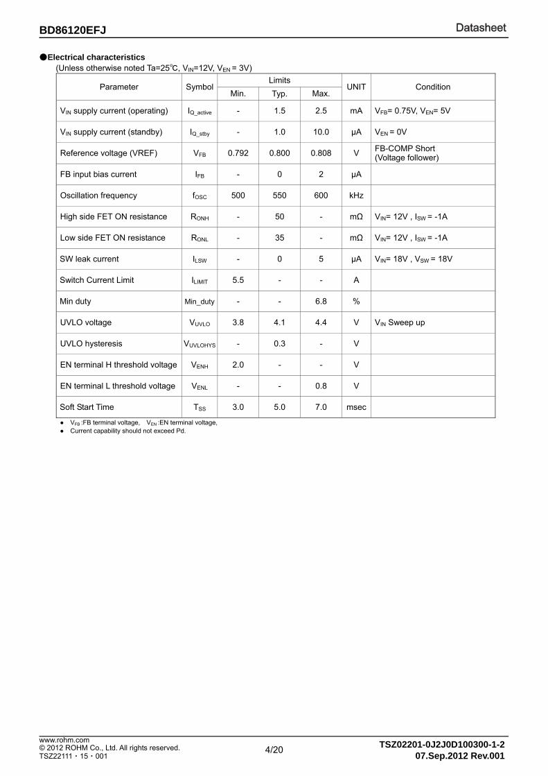
Features Input voltage range: 4.5V to 18.0V Reference voltage 0.8V ± 1% Average output Current: 5A(Max.) Switching frequency: 550kHz(Typ.) Pch FET ON resistance: 50mΩ(Typ.) Nch FET ON resistance: 35mΩ(Typ.) Standby current: 1μA (Typ.) Operating temperature range: -40 to +85 Cycle by cycle over current protection(OCP) Thermal shutdown (TSD) Under voltage lock out(UVLO) Short circuit protection(SCP) Over voltage protection(OVP) Fixed soft start 5msec
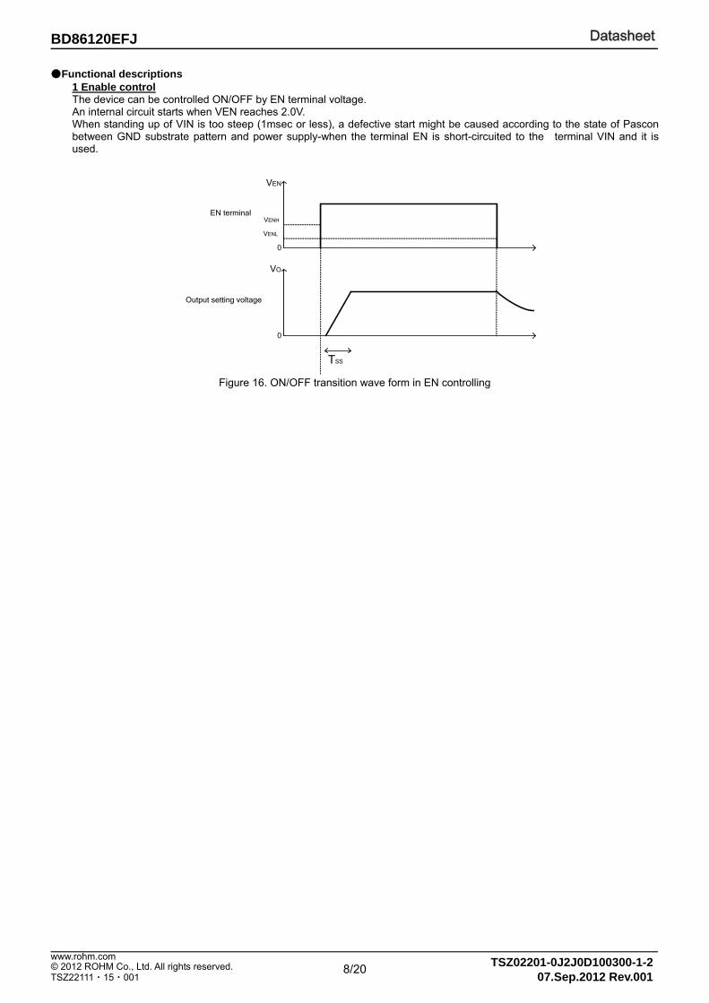
Functional descriptions 1 Enable control The device can be controlled ON/OFF by EN terminal voltage. An internal circuit starts when VEN reaches 2.0V. When standing up of VIN is too steep (1msec or less), a defective start might be caused according to the state of Pascon between GND substrate pattern and power supply-when the terminal EN is short-circuited to the terminal VIN and it is used.
VEN
0
VO
0
TSS
VENH
VENL
EN terminal
Output setting voltage
Figure 16. ON/OFF transition wave form in EN controlling
Protection circuit is effective for destruction prevention due to accident so that avoid using under continuous protection operation.
2-1 Short Circuit protection function (SCP) The FB terminal voltage is compared with internal reference voltage VREF. If FB terminal voltage falls below VSCP (= VREF - 240mV) and the state continues, output changes to low voltage and the state is fixed. During soft start, the FB terminal voltage is compared with internal soft start slope
Table 1 output short circuit protection function
EN terminal FB terminal Short Circuit Protection function
Short Circuit Protection operation
>VENH <VSCP
Effective ON
>VSCP OFF
<VENL - Invalidity OFF
0.8V
SCP threshold:0.56V
SCP delay timeTyp:1msec
SCP release before counter fix
SCP delay timeTyp:1msec
SCP ProtectHG=HLG=L
OCP threshold
VOUT1
FB
LG
HG
EN
IL
EN threshold
Soft startTyp:1msec
latch release by EN or UVLO
Normal operation Normal operationSCP
(OFF Latch)Stand byNormal operationOCP OCP
HG Hi side FET GATE signalLG : Low side FET GATE signal
2-2 Over voltage protection function (OVP) Output over Voltage Protection is activated when FB voltage rises to or above VOVP (= VREF + 240mV) and the state
continues, output changes to low voltage and the state is fixed. Table 2 output over voltage protection function
EN terminal FB terminal Short Circuit Protection function
Short Circuit Protection operation
>VENH >VOVP
Effective ON
<VOVP OFF
<VENL - Invalidity OFF
VOUT
FB
HG
LG
EN
0.8V
OVP delay timeTyp:1msec
OVP delay timeTyp : 1msec
latch release by EN or UVLO
OVP release before counter fix
Soft startTyp:1msec
Release Abnormal state
1.04V
EN Threshold
switching restart
OVP ProtectHG:Hi LG:Low
Normal operation Normal operationOVP
(OFF Latch)Stand by
HG : Hi side FET GATE signalLG : Low side FET GATE signal
2-3 Under voltage lock out protection (UVLO) Under voltage lock out protection monitors the VIN terminal voltage.
When the VIN terminal voltage is lower than 3.8V (typ), the device state changes to the standby mode. When the VIN terminal voltage is higher than 4.1V (typ), the device starts operation.
VIN
0
Vo
HG
LG
FB
Soft Start
hys
UVLO Release
UVLO detection
Normal operation Normal operationUVLO
HG : Hi side FET GATE signalLG : Low side FET GATE signal
Figure 19. UVLO Timing chart
2-4 Thermal shut down function BD86120 monitors the temperature of itself. When the temperature of the chip exceeds Tj=175, the DC/DC converter is fixed in a low voltage. TSD function is aimed to shut down IC from thermal reckless driving under an abnormal state to exceed Tjmax=150. It aims at neither protection nor the guarantee of the set. Therefore, please do not use this function to protect the set.
VIN
EN
Vout
Tj
HG
LG
SCP threshold
SCP delay timeTyp:1msec
Soft Start
TSD release
TSDNormal operation Normal operation TSDSCP
(OFF Latch)Normal operation
TSD release HG : Hi side FET GATE signalLG : Low side FET GATE signal
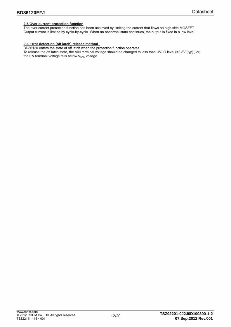
2-5 Over current protection function The over current protection function has been achieved by limiting the current that flows on high side MOSFET. Output current is limited by cycle-by-cycle. When an abnormal state continues, the output is fixed in a low level. 2-6 Error detection (off latch) release method BD86120 enters the state of off latch when the protection function operates. To release the off latch state, the VIN terminal voltage should be changed to less than UVLO level (=3.8V [typ] ) or, the EN terminal voltage falls below VENL.voltage.
The Output LC filter is required to supply constant current to the output load. A larger value inductance at this filter results in less inductor ripple current(∆IL) and less output ripple voltage. However, the larger value inductors tend to have less fast load transient-response, a larger physical size, a lower saturation current and higher series resistance. A smaller value inductance has almost opposite characteristics above. So Choosing the Inductor ripple current(∆IL) between 20 to 40% of the averaged inductor current (equivalent to the output load current) is a good compromise.
Figure 22. Figure 23. Setting ∆IL = 30% x Averaged Inductor current (4A) = 1.2 [A],
L = VOUT (VIN - VOUT) 1
= 3.6µ ≒ 3.3µ [H] VIN FOSC ∆IL
Where VIN= 12V, VOUT= 3.3V, FOSC= 550 kHz, ; FOSC is a switching frequency Also the inductor should have the higher saturation current than IOUTMAX + ∆IL / 2. The output capacitor COUT affects the output ripple-voltage. Choose the large capacitor to achieve the small ripple-voltage enough to meet the application requirement.
Output ripple voltage ∆VRPL is calculated by the following equation.
Where RESR is a parasitic series resistance in output capacitor. Setting COUT = 44uF, RESR = 10mΩ ∆VRPL = 1.2 (10m + 1 / (8 44µ 550k)) = 18.2mV
(2) Design of Feedback Resistance constant
Set the feedback resistance as shown below.
Figure 24.
∆VRPL = ∆IL ( RESR + 1
) [V] 8 COUT FOSC
VOUT = R1 + R2
0.8 [V] R2
IL
t
IOUTMAX + IL /2 should not reach the rated value level
(3)Loop Compensation Choosing compensation capacitor CCMP and resistor RCMP
The current-mode buck converter has 2-poles and 1-zero system. Choosing the compensation resistor and capacitor is important for a good load-transient response and good stability. The example of DC/DC converter application bode plot is shown below. The compensation resistor RCMP will decides the cross over frequency FCRS (the frequency that the total DC-DC loop-gain falls to 0dB). Setting the higher cross over frequency achieves good response speed, however less stability. While setting the lower cross over frequency shows good stability but worse response speed. The 1/10 of switching frequency for the cross over frequency shows a good performance at most applications. ( i ) Choosing phase compensation resistor RCMP The compensation resistor RCMP can be on following formula.
Where VOUT ; Output voltage, FCRS ; Cross over frequency, COUT ; Output Capacitor, VFB ; internal feedback voltage (0.8V(TYP)), GMP ; Current Sense Gain (8.6A/V(TYP)) , GMA ; Error Amplifier Trans-conductance (400µA/V(TYP))
Setting VOUT= 3.3V, FCRS= 55kHz, COUT= 44µF、
( ii ) Choosing phase compensation capacitor CCMP For the stability of DC/DC converter, canceling the phase delay that derives from output capacitor COUT and resistive load ROUT by inserting the phase advance. The phase advance can be added by the zero on compensation resistor RCMP and capacitor CCMP. Making Fz= FCRS / 6 gives a first-order estimate of CCMP.
However, the best values of zero and FCRS are different between applications. After calculation above formula and confirmation actual application, please decide values finally. ( iii ) The condition of the loop compensation stability The stability of DC/DC converter is important. To secure the operating stability, please check the loop compensation has
the enough phase-margin. For the condition of loop compensation stability, the phase-delay must be less than 150 degree where Gain is 0 dB. Feed forward capacitor CRUP boosts phase margin over a limited frequency range and is sometimes used to improve
loop response. CRUP will be more effective if RUP >> RUP||RDW
Use of the IC in excess of absolute maximum ratings such as the applied voltage or operating temperature range may result in IC damage. Assumptions should not be made regarding the state of the IC (short mode or open mode) when such damage is suffered. A physical safety measure such as a fuse should be implemented when use of the IC in a special mode where the absolute maximum ratings may be exceeded is anticipated.
2) GND potential Ensure a minimum GND pin potential in all operating conditions.
3) Setting of heat Use a thermal design that allows for a sufficient margin in light of the power dissipation (Pd) in actual operating conditions.
4) Pin short and mistake fitting Use caution when orienting and positioning the IC for mounting on printed circuit boards. Improper mounting may result in damage to the IC. Shorts between output pins or between output pins and the power supply and GND pins caused by the presence of a foreign object may result in damage to the IC.
5) Actions in strong magnetic field Use caution when using the IC in the presence of a strong magnetic field as doing so may cause the IC to malfunction.
6) Testing on application boards When testing the IC on an application board, connecting a capacitor to a pin with low impedance subjects the IC to stress. Always discharge capacitors after each process or step. Ground the IC during assembly steps as an antistatic measure, and use similar caution when transporting or storing the IC. Always turn the IC's power supply off before connecting it to or removing it from a jig or fixture during the inspection process.
7) Ground wiring patterns When using both small signal and large current GND patterns, it is recommended to isolate the two ground patterns, placing a single ground point at the application's reference point so that the pattern wiring resistance and voltage variations caused by large currents do not cause variations in the small signal ground voltage. Be careful not to change the GND wiring patterns of any external components.
8) Regarding input pin of the IC This monolithic IC contains P+ isolation and P substrate layers between adjacent elements in order to keep them isolated. P/N junctions are formed at the intersection of these P layers with the N layers of other elements to create a variety of parasitic elements. For example, when the resistors and transistors are connected to the pins as shown in Figure 26. , a parasitic diode or a transistor operates by inverting the pin voltage and GND voltage. The formation of parasitic elements as a result of the relationships of the potentials of different pins is an inevitable result of the IC's architecture. The operation of parasitic elements can cause interference with circuit operation as well as IC malfunction and damage. For these reasons, it is necessary to use caution so that the IC is not used in a way that will trigger the operation of parasitic elements such as by the application of voltages lower than the GND (P substrate) voltage to input and output pins.
Figure 28. Example of a Simple Monolithic IC Architecture
An overcurrent protection circuit designed according to the output current is incorporated for the prevention of IC damage that may result in the event of load shorting. This protection circuit is effective in preventing damage due to sudden and unexpected accidents. However, the IC should not be used in applications characterized by the continuous operation or transitioning of the protection circuits. At the time of thermal designing, keep in mind that the current capacity has negative characteristics to temperatures.
10) Thermal shutdown circuit (TSD) This IC incorporates a built-in TSD circuit for the protection from thermal destruction. The IC should be used within the specified power dissipation range. However, in the event that the IC continues to be operated in excess of its power dissipation limits, the attendant rise in the chip's junction temperature Tj will trigger the TSD circuit to turn off all output power elements. Operation of the TSD circuit presumes that the IC's absolute maximum ratings have been exceeded. Application designs should never make use of the TSD circuit.
11) EN control speed Chattering happens if standing lowering speed is slow when standing of EN pin is lowered. The reverse current in which the input side and the pressure operation are done from the output side is generated when chattering operates with the output voltage remained, and there is a case to destruction. Please set to stand within 100µs when you control ON/OFF by the EN signal.
Status of this document The Japanese version of this document is formal specification. A customer may use this translation version only for a reference to help reading the formal version. If there are any differences in translation version of this document formal version takes priority