AND MEDICAL APPLICATIONS2• Qualified for Automotive Applications
• Controlled Baseline• Wide Input Voltage Range: 5.5 V to 36 V• One Assembly/Test Site• Up to 5-A Continuous (6-A Peak) Output• One Fabrication SiteCurrent• Available in Military (–55°C/125°C)• High Efficiency Greater than 90% Enabled by
Temperature Range (1)110-mΩ Integrated MOSFET Switch
• Extended Product Life Cycle• Wide Output Voltage Range: Adjustable Down• Extended Product-Change Notificationto 1.22 V with 1.5% Initial Accuracy• Product Traceability• Internal Compensation Minimizes External
Parts Count• Fixed 500-kHz Switching Frequency for Small
As a member of the SWIFT™ family of DC/DCFilter Sizeregulators, the TPS5450 is a high-output-current• 18-µA Shutdown Supply Current PWM converter that integrates a low-resistance
• Improved Line Regulation and Transient high-side N-channel MOSFET. Included on theResponse by Input Voltage Feed Forward substrate with the listed features are a
high-performance voltage error amplifier that provides• System Protected by Overcurrent Limiting,tight voltage regulation accuracy under transientOvervoltage Protection, and Thermalconditions, an undervoltage-lockout circuit to preventShutdown start-up until the input voltage reaches 5.5 V, an
• Available in Small Thermally Enhanced 8-Pin internally set slow-start circuit to limit inrush currents,SOIC PowerPAD™ Package and a voltage feed-forward circuit to improve the
transient response. Using the ENA pin, shutdown• For SWIFT™ Documentation, Applicationsupply current is reduced to 18 µA typically. OtherReports and Design Software, See the TIfeatures include an active-high enable, overcurrentWebsite at www.ti.com/swiftlimiting, overvoltage protection, and thermalshutdown. To reduce design complexity and externalcomponent count, the TPS5450 feedback loop is
• High-Density Point-of-Load Regulators internally compensated.• LCD Displays, Plasma Displays The TPS5450 device is available in a thermally• Battery Chargers enhanced, 8-pin SOIC PowerPAD™ package. TI• 12-V/24-V Distributed Power Systems provides evaluation modules and software tools to aid
in achieving high-performance power supply designsto meet aggressive equipment development cycles.(1) Additional temperature ranges are available - contact factory
1
Please be aware that an important notice concerning availability, standard warranty, and use in critical applications of TexasInstruments semiconductor products and disclaimers thereto appears at the end of this data sheet.
2SWIFT, PowerPAD are trademarks of Texas Instruments.
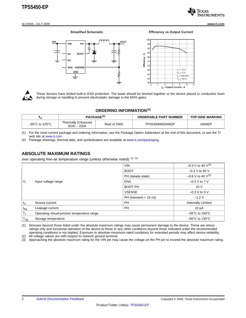
These devices have limited built-in ESD protection. The leads should be shorted together or the device placed in conductive foamduring storage or handling to prevent electrostatic damage to the MOS gates.
ORDERING INFORMATION (1)
TA PACKAGE (2) ORDERABLE PART NUMBER TOP-SIDE MARKINGThermally Enhanced–55°C to 125°C Reel of 2500 TPS5450MDDAREP 5450EPSOIC – DDA
(1) For the most current package and ordering information, see the Package Option Addendum at the end of this document, or see the TIweb site at www.ti.com.
(2) Package drawings, thermal data, and symbolization are available at www.ti.com/packaging.
over operating free-air temperature range (unless otherwise noted) (1) (2)
VIN –0.3 V to 40 V (3)
BOOT –0.3 V to 50 VPH (steady-state) –0.6 V to 40 V (3)
VI Input voltage range ENA –0.3 V to 7 VBOOT-PH 10 VVSENSE –0.3 V to 3 VPH (transient < 10 ns) –1.2 V
IO Source current PH Internally LimitedIlkg Leakage current PH 10 µATJ Operating virtual-junction temperature range –55°C to 150°CTstg Storage temperature –65°C to 150°C
(1) Stresses beyond those listed under the absolute maximum ratings may cause permanent damage to the device. These are stressratings only and functional operation of the device at these or any other conditions beyond those indicated under the recommendedoperating conditions is not implied. Exposure to absolute-maximum-rated conditions for extended periods may affect device reliability.
(2) All voltage values are with respect to network ground terminal.(3) Approaching the absolute maximum rating for the VIN pin may cause the voltage on the PH pin to exceed the absolute maximum rating.
THERMAL IMPEDANCEPACKAGE JUNCTION-TO-AMBIENT8-Pin DDA (4-layer board with solder) (3) 30°C/W
(1) Maximum power dissipation may be limited by overcurrent protection.(2) Power rating at a specific ambient temperature TA should be determined with a junction temperature of 125°C. This is the point where
distortion starts to substantially increase. Thermal management of the final PCB should strive to keep the junction temperature at orbelow 125°C for best performance and long-term reliability. See Thermal Calculations in applications section of this data sheet for moreinformation.
(3) Test board conditions:a. 2 in x 1.85 in, 4 layers, 0.062-in (1,57-mm) thicknessb. 2-oz copper traces located on the top and bottom of the PCBc. 2-oz copper ground planes on the two internal layersd. Four thermal vias in the PowerPAD area under the device package
MIN MAX UNITVI Input voltage range 5.5 36 VTJ Operating junction temperature –55 125 °C
TJ = –55°C to 125°C, VIN = 5.5 V to 36 V (unless otherwise noted)
PARAMETER TEST CONDITIONS MIN TYP MAX UNITSUPPLY VOLTAGE (VIN PIN)
VSENSE = 2 V, Not switching, PH pin open 3 4.4 mAIQ Quiescent current
Shutdown, ENA = 0 V 18 60 µAUNDERVOLTAGE LOCK OUT (UVLO)
Voltage reference accuracy VIO = 0 A – 5 A; TJ = Full Range 1.193 1.221 1.245
OSCILLATORTJ = 25°C 400 500 600 kHz
Internally set free-running frequencyTJ = Full Range 375 500 600
Minimum controllable on time 150 220 nsMaximum duty cycle 87 89 %
ENABLE (ENA PIN)Start threshold voltage, ENA 1.3 VStop threshold voltage, ENA 0.5 VHysteresis voltage, ENA 450 mVInternal slow-start time (0~100%) 5.4 8 10 ms
CURRENT LIMITTJ = 25°C 6.0 7.5 9.0 A
Current limitTJ = Full Range 4.4 7.5 11.7TJ = 25°C 13 16 20 ms
Current limit hiccup timeTJ = Full Range 13 16 22.5
THERMAL SHUTDOWNThermal shutdown trip point 135 162 °CThermal shutdown hysteresis 14 °C
ELECTRICAL CHARACTERISTICS (continued)TJ = –55°C to 125°C, VIN = 5.5 V to 36 V (unless otherwise noted)
PARAMETER TEST CONDITIONS MIN TYP MAX UNITOUTPUT MOSFET
VIN = 5.5 V 150rDS(on) High-side power MOSFET switch mΩ
110
TERMINAL FUNCTIONSTERMINAL
DESCRIPTIONNAME NO.BOOT 1 Boost capacitor for the high-side FET gate driver. Connect 0.01-µF low-ESR capacitor from BOOT pin to PH pin.NC 2, 3 No internal connectionVSENSE 4 Feedback voltage for the regulator. Connect to output voltage divider.ENA 5 On/off control. Below 0.5 V, the device stops switching. Float the pin to enable.GND 6 Ground. Connect to thermal pad.
Input supply voltage. Bypass VIN pin to GND pin close to device package with a high-quality low-ESR ceramicVIN 7 capacitor.PH 8 Source of the high side power MOSFET. Connected to external inductor and diode.PowerPAD 9 GND pin must be connected to the exposed pad for proper operation.
The internal free-running oscillator sets the PWM switching frequency at 500 kHz. The 500-kHz switchingfrequency allows less output inductance for the same output ripple requirement resulting in a smaller outputinductor.
The voltage reference system produces a precision reference signal by scaling the output of a temperaturestable bandgap circuit. The bandgap and scaling circuits are trimmed during production testing to an output of1.221 V at room temperature.
The ENA pin provides electrical on/off control of the regulator. Once the ENA pin voltage exceeds the thresholdvoltage, the regulator starts operation and the internal slow start begins to ramp. If the ENA pin voltage is pulledbelow the threshold voltage, the regulator stops switching and the internal slow start resets. Connecting the pinto ground or to any voltage less than 0.5 V disables the regulator and activates the shutdown mode. Thequiescent current of the TPS5450 in shutdown mode is 18 µA (typical).
The ENA pin has an internal pullup current source, allowing the user to float the ENA pin. If an applicationrequires controlling the ENA pin, use open drain or open collector output logic to interface with the pin. To limitthe start-up inrush current, an internal slow-start circuit is used to ramp up the reference voltage from 0 V to itsfinal value, linearly. The internal slow start time is 8 ms (typical).
The TPS5450 incorporates an undervoltage lockout circuit to keep the device disabled when VIN (the inputvoltage) is below the UVLO start voltage threshold. During power up, internal circuits are held inactive and theinternal slow start is grounded until VIN exceeds the UVLO start threshold voltage. Once the UVLO startthreshold voltage is reached, the internal slow start is released and device start-up begins. The device operatesuntil VIN falls below the UVLO stop threshold voltage. The typical hysteresis in the UVLO comparator is 330 mV.
Connect a 0.01-µF low-ESR ceramic capacitor between the BOOT pin and PH pin. This capacitor provides thegate drive voltage for the high-side MOSFET. X7R or X5R grade dielectrics are recommended due to their stablevalues over temperature.
The output voltage of the regulator is set by feeding back the center point voltage of an external resistor dividernetwork to the VSENSE pin. In steady-state operation, the VSENSE pin voltage should be equal to the voltagereference 1.221 V.
The TPS5450 implements internal compensation to simplify the regulator design. Because the TPS5450 usesvoltage-mode control, a type 3 compensation network has been designed on chip to provide a high crossoverfrequency and a high phase margin for good stability. See the Internal Compensation Network section for moredetails.
The internal voltage feed forward provides a constant dc power stage gain despite any variations with the inputvoltage. This greatly simplifies the stability analysis and improves the transient response. Voltage feed forwardvaries the peak ramp voltage inversely with the input voltage so that the modulator and power stage gain areconstant at the feed forward gain:
The typical feed forward gain of TPS5450 is 25.
The regulator employs a fixed frequency pulse-width-modulator (PWM) control method. First, the feedbackvoltage (VSENSE pin voltage) is compared to the constant voltage reference by the high-gain error amplifier andcompensation network to produce a error voltage. Then, the error voltage is compared to the ramp voltage by thePWM comparator. In this way, the error-voltage magnitude is converted to a pulse width, which is the duty cycle.Finally, the PWM output is fed into the gate drive circuit to control the on-time of the high-side MOSFET.
Overcurrent limiting is implemented by sensing the drain-to-source voltage across the high-side MOSFET. Thedrain to source voltage is then compared to a voltage level representing the overcurrent threshold limit. If thedrain-to-source voltage exceeds the overcurrent threshold limit, the overcurrent indicator is set true. The systemignores the overcurrent indicator for the leading edge blanking time at the beginning of each cycle to avoid anyturn-on noise glitches.
Once overcurrent indicator is set true, overcurrent limiting is triggered. The high-side MOSFET is turned off forthe rest of the cycle after a propagation delay. The overcurrent limiting mode is called cycle-by-cycle currentlimiting.
Sometimes under serious overload conditions such as short-circuit, the overcurrent runaway may still happenwhen using cycle-by-cycle current limiting. A second mode of current limiting is used, i.e. hiccup modeovercurrent limiting. During hiccup mode overcurrent limiting, the voltage reference is grounded and the high-sideMOSFET is turned off for the hiccup time. Once the hiccup time duration is complete, the regulator restarts undercontrol of the slow start circuit.
The TPS5450 has an overvoltage protection (OVP) circuit to minimize voltage overshoot when recovering fromoutput fault conditions. The OVP circuit includes an overvoltage comparator to compare the VSENSE pin voltageand a threshold of 112.5% × VREF. Once the VSENSE pin voltage is higher than the threshold, the high-sideMOSFET is forced off. When the VSENSE pin voltage drops lower than the threshold, the high-side MOSFET isenabled again.
The TPS5450 protects itself from overheating with an internal thermal shutdown circuit. If the junctiontemperature exceeds the thermal shutdown trip point, the voltage reference is grounded and the high-sideMOSFET is turned off. The part is restarted under control of the slow start circuit automatically when the junctiontemperature drops 14°C below the thermal shutdown trip point.
Connect a low ESR ceramic bypass capacitor to the VIN pin. Care should be taken to minimize the loop areaformed by the bypass capacitor connections, the VIN pin, and the TPS5450 ground pin. The best way to do thisis to extend the top side ground area from under the device adjacent to the VIN trace, and place the bypasscapacitor as close as possible to the VIN pin. The minimum recommended bypass capacitance is 4.7 µF ceramicwith a X5R or X7R dielectric.
There should be a ground area on the top layer directly underneath the IC, with an exposed area for connectionto the PowerPAD. Use vias to connect this ground area to any internal ground planes. Use additional vias at theground side of the input and output filter capacitors as well. The GND pin should be tied to the PCB ground byconnecting it to the ground area under the device as shown below.
The PH pin should be routed to the output inductor, catch diode and boot capacitor. Since the PH connection isthe switching node, the inductor should be located very close to the PH pin and the area of the PCB conductorminimized to prevent excessive capacitive coupling. The catch diode should also be placed close to the device tominimize the output current loop area. Connect the boot capacitor between the phase node and the BOOT pin asshown. Keep the boot capacitor close to the IC and minimize the conductor trace lengths. The componentplacements and connections shown work well, but other connection routings also may be effective.
Connect the output filter capacitor(s) as shown between the VOUT trace and GND. It is important to keep theloop formed by the PH pin, Lout, Cout and GND as small as is practical.
Connect the VOUT trace to the VSENSE pin using the resistor divider network to set the output voltage. Do notroute this trace too close to the PH trace. Due to the size of the IC package and the device pin-out, the tracemay need to be routed under the output capacitor. Alternately, the routing may be done on an alternate layer if atrace under the output capacitor is not desired.
If using the grounding scheme shown in Figure 9, use a via connection to a different layer to route to the ENApin.
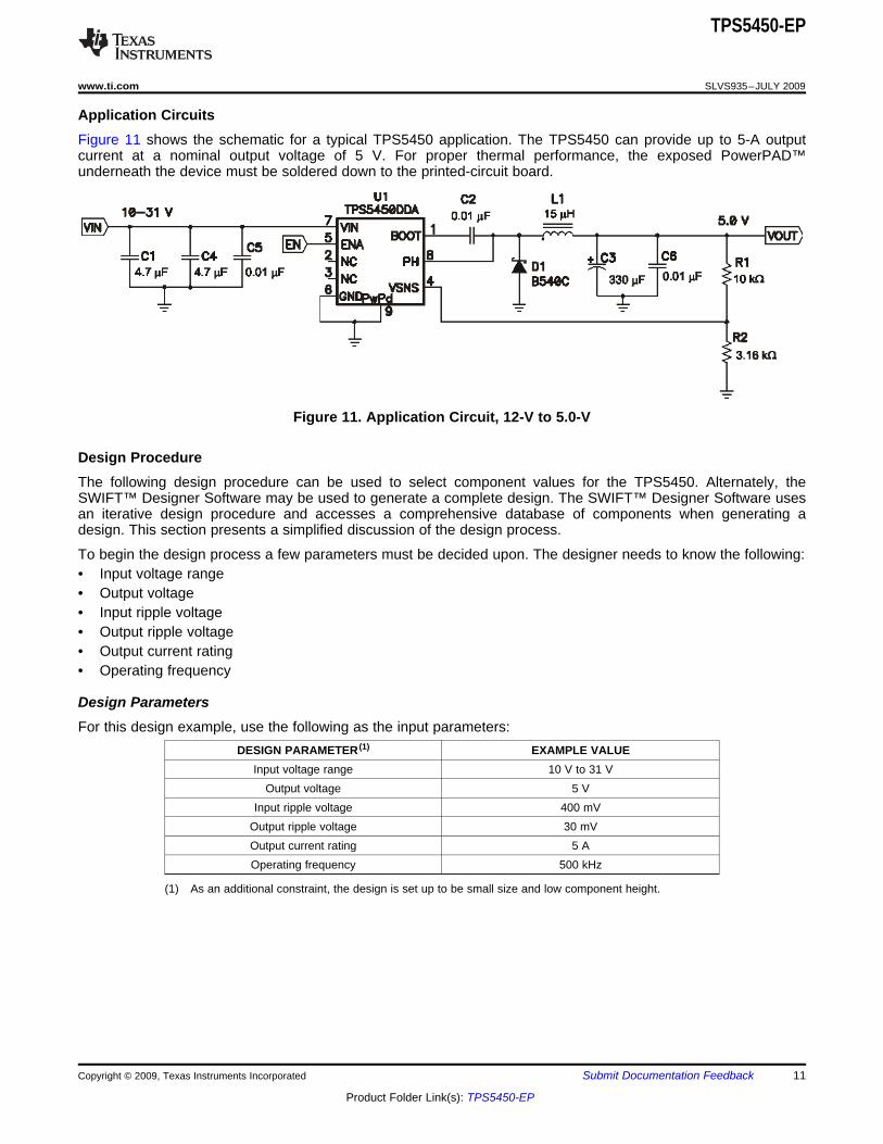
Figure 11 shows the schematic for a typical TPS5450 application. The TPS5450 can provide up to 5-A outputcurrent at a nominal output voltage of 5 V. For proper thermal performance, the exposed PowerPAD™underneath the device must be soldered down to the printed-circuit board.
Figure 11. Application Circuit, 12-V to 5.0-V
The following design procedure can be used to select component values for the TPS5450. Alternately, theSWIFT™ Designer Software may be used to generate a complete design. The SWIFT™ Designer Software usesan iterative design procedure and accesses a comprehensive database of components when generating adesign. This section presents a simplified discussion of the design process.
To begin the design process a few parameters must be decided upon. The designer needs to know the following:• Input voltage range• Output voltage• Input ripple voltage• Output ripple voltage• Output current rating• Operating frequency
Design ParametersFor this design example, use the following as the input parameters:
DESIGN PARAMETER (1) EXAMPLE VALUEInput voltage range 10 V to 31 V
Output voltage 5 VInput ripple voltage 400 mV
Output ripple voltage 30 mVOutput current rating 5 AOperating frequency 500 kHz
(1) As an additional constraint, the design is set up to be small size and low component height.
Switching FrequencyThe switching frequency for the TPS5450 is internally set to 500 kHz. It is not possible to adjust the switchingfrequency.
Input CapacitorsThe TPS5450 requires an input decoupling capacitor and, depending on the application, a bulk input capacitor.The minimum recommended decoupling capacitance is 4.7 µF. A high-quality ceramic type X5R or X7R isrequired. For some applications, a smaller value decoupling capacitor may be used, so long as the input voltageand current ripple ratings are not exceeded. The voltage rating must be greater than the maximum input voltage,including ripple.
This input ripple voltage can be approximated by Equation 2 :
Where IOUT(MAX) is the maximum load current, fSW is the switching frequency, CIN is the input capacitor value andESRMAX is the maximum series resistance of the input capacitor. For this design, the input capacitance consistsof two 4.7 µF capacitors, C1 and C4, in parallel. An additional high-frequency bypass capacitor, C5 is also used.
The maximum RMS ripple current also needs to be checked. For worst case conditions, this can beapproximated by Equation 3 :
In this case the input ripple voltage would be 281 mV and the RMS ripple current would be 2.5 A. The maximumvoltage across the input capacitors would be VIN max plus delta VIN/2. The chosen input decoupling capacitor israted for 50 V, and the ripple current capacity is greater than 2.5 A each, providing ample margin. It is veryimportant that the maximum ratings for voltage and current are not exceeded under any circumstance.
Additionally some bulk capacitance may be needed, especially if the TPS5450 circuit is not located within about2 inches from the input voltage source. The value for this capacitor is not critical but it also should be rated tohandle the maximum input voltage including ripple voltage and should filter the output so that input ripple voltageis acceptable.
Output Filter ComponentsTwo components need to be selected for the output filter, L1 and C2. Because the TPS5450 is an internallycompensated device, a limited range of filter component types and values can be supported.
Inductor Selection
To calculate the minimum value of the output inductor, use Equation 4:
KIND is a coefficient that represents the amount of inductor ripple current relative to the maximum output current.Three things need to be considered when determining the amount of ripple current in the inductor: thepeak-to-peak ripple current affects the output ripple voltage amplitude, the ripple current affects the peak switchcurrent, and the amount of ripple current determines at what point the circuit becomes discontinuous. Fordesigns using the TPS5450, KIND of 0.2 to 0.3 yields good results. Low output ripple voltages can be obtainedwhen paired with the proper output capacitor, the peak switch current will be well below the current limit set point,and relatively low load currents can be sourced before discontinuous operation.
For this design example use KIND = 0.2 and the minimum inductor value is calculated to be 10.4 µH. A higherstandard value is 15 µH, which is used in this design.
For the output filter inductor it is important that the RMS current and saturation current ratings not be exceeded.The RMS inductor current can be found from Equation 5:
and the peak inductor current can be determined with Equation 6:
For this design, the RMS inductor current is 5.004 A, and the peak inductor current is 5.34 A. The choseninductor is a Sumida CDRH1127/LD-150 15µH. It has a minimum rated current of 5.65 A for both saturation andRMS current. In general, inductor values for use with the TPS5450 are in the range of 10 µH to 100 µH.
Capacitor Selection
The important design factors for the output capacitor are dc voltage rating, ripple current rating, and equivalentseries resistance (ESR). The dc voltage and ripple current ratings cannot be exceeded. The ESR is importantbecause, along with the inductor ripple current, it determines the amount of output ripple voltage. The actualvalue of the output capacitor is not critical, but some practical limits do exist. Consider the relationship betweenthe desired closed loop crossover frequency of the design and LC corner frequency of the output filter. Due tothe design of the internal compensation, it is desirable to keep the closed loop crossover frequency in the range3 kHz to 30 kHz, as this frequency range has adequate phase boost to allow for stable operation. For this designexample, it is assumed that the intended closed loop crossover frequency is between 2590 Hz and 24 kHz andalso below the ESR zero of the output capacitor. Under these conditions the closed loop crossover frequency isrelated to the LC corner frequency by:
And the desired output capacitor value for the output filter to:
For a desired crossover of 12 kHz and a 15-µH inductor, the calculated value for the output capacitor is 330 µF.The capacitor type should be chosen so that the ESR zero is above the loop crossover. The maximum ESRshould be:
The maximum ESR of the output capacitor also determines the amount of output ripple as specified in the initialdesign parameters. The output ripple voltage is the inductor ripple current times the ESR of the output filter.Check that the maximum specified ESR as listed in the capacitor data sheet results in an acceptable outputripple voltage:
Where:ΔVPP is the desired peak-to-peak output ripple.NC is the number of parallel output capacitors.FSW is the switching frequency.
For this design example, a single 330-µF output capacitor is chosen for C3. The calculated RMS ripple current is143 mA and the maximum ESR required is 40 mΩ. A capacitor that meets these requirements is a SanyoPoscap 10TPB330M, rated at 10 V with a maximum ESR of 35 mΩ and a ripple current rating of 3 A. Anadditional small 0.1-µF ceramic bypass capacitor, C6 is also used in this design.
The minimum ESR of the output capacitor should also be considered. For good phase margin, the ESR zerowhen the ESR is at a minimum should not be too far above the internal compensation poles at 24 kHz and54 kHz.
The selected output capacitor must also be rated for a voltage greater than the desired output voltage plus onehalf the ripple voltage. Any derating amount must also be included. The maximum RMS ripple current in theoutput capacitor is given by Equation 11:
Where:NC is the number of output capacitors in parallel.FSW is the switching frequency.
Other capacitor types can be used with the TPS5450, depending on the needs of the application.
Output Voltage SetpointThe output voltage of the TPS5450 is set by a resistor divider (R1 and R2) from the output to the VSENSE pin.Calculate the R2 resistor value for the output voltage of 5 V using Equation 12:
For any TPS5450 design, start with an R1 value of 10 kΩ. For an output voltage closest to but at least 5 V, R2 is3.16 kΩ.
Boot CapacitorThe boot capacitor should be 0.01 µF.
Catch DiodeThe TPS5450 is designed to operate using an external catch diode between PH and GND. The selected diodemust meet the absolute maximum ratings for the application: Reverse voltage must be higher than the maximumvoltage at the PH pin, which is VINMAX + 0.5 V. Peak current must be greater than IOUTMAX plus on half thepeak to peak inductor current. Forward voltage drop should be small for higher efficiencies. It is important to notethat the catch diode conduction time is typically longer than the high-side FET on time, so attention paid to diodeparameters can make a marked improvement in overall efficiency. Additionally, check that the device chosen iscapable of dissipating the power losses. For this design, a Diodes, Inc. B540A is chosen, with a reverse voltageof 40 V, forward current of 5 A, and a forward voltage drop of 0.5 V.
Due to the internal design of the TPS5450, there are both upper and lower output voltage limits for any giveninput voltage. The upper limit of the output voltage set point is constrained by the maximum duty cycle of 87%and is given by:
WhereVINMIN = minimum input voltageIOMAX = maximum load currentVD = catch diode forward voltage.RL= output inductor series resistance.
This equation assumes maximum on resistance for the internal high side FET.
The lower limit is constrained by the minimum controllable on time, which may be as high as 200 ns. Theapproximate minimum output voltage for a given input voltage and minimum load current is given by:
WhereVINMAX = maximum input voltageIOMIN = minimum load currentVD = catch diode forward voltage.RL= output inductor series resistance.This equation assumes nominal on resistance for the high-side FET and accounts for worst case variation ofoperating frequency set point. Any design operating near the operational limits of the device should becarefully checked to ensure proper functionality.
The design equations given in the example circuit can be used to generate circuits using the TPS5450. Thesedesigns are based on certain assumptions and will tend to always select output capacitors within a limited rangeof ESR values. If a different capacitor type is desired, it may be possible to fit one to the internal compensation ofthe TPS5450. Equation 15 gives the nominal frequency response of the internal voltage-mode type IIIcompensation network:
Using this information along with the desired output voltage, feed forward gain and output filter characteristics,the closed loop transfer function can be derived.
The following formulas show how to estimate the device power dissipation under continuous conduction modeoperations. They should not be used if the device is working at light loads in the discontinuous conduction mode.
Conduction Loss: Pcon = IOUT2 x RDS(on) x VOUT/VIN
Switching Loss: Psw = VIN x IOUT x 0.01Quiescent Current Loss: Pq = VIN x 0.01Total Loss: Ptot = Pcon + Psw + PqGiven TA => Estimated Junction Temperature: TJ = TA + Rth x PtotGiven TJMAX = 125°C => Estimated Maximum Ambient Temperature: TAMAX = TJMAX – Rth x Ptot
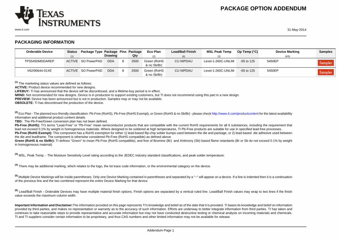
TPS5450MDDAREP ACTIVE SO PowerPAD DDA 8 2500 Green (RoHS& no Sb/Br)
CU NIPDAU Level-1-260C-UNLIM -55 to 125 5450EP
V62/90644-01XE ACTIVE SO PowerPAD DDA 8 2500 Green (RoHS& no Sb/Br)
CU NIPDAU Level-1-260C-UNLIM -55 to 125 5450EP
(1) The marketing status values are defined as follows:ACTIVE: Product device recommended for new designs.LIFEBUY: TI has announced that the device will be discontinued, and a lifetime-buy period is in effect.NRND: Not recommended for new designs. Device is in production to support existing customers, but TI does not recommend using this part in a new design.PREVIEW: Device has been announced but is not in production. Samples may or may not be available.OBSOLETE: TI has discontinued the production of the device.
(2) Eco Plan - The planned eco-friendly classification: Pb-Free (RoHS), Pb-Free (RoHS Exempt), or Green (RoHS & no Sb/Br) - please check http://www.ti.com/productcontent for the latest availabilityinformation and additional product content details.TBD: The Pb-Free/Green conversion plan has not been defined.Pb-Free (RoHS): TI's terms "Lead-Free" or "Pb-Free" mean semiconductor products that are compatible with the current RoHS requirements for all 6 substances, including the requirement thatlead not exceed 0.1% by weight in homogeneous materials. Where designed to be soldered at high temperatures, TI Pb-Free products are suitable for use in specified lead-free processes.Pb-Free (RoHS Exempt): This component has a RoHS exemption for either 1) lead-based flip-chip solder bumps used between the die and package, or 2) lead-based die adhesive used betweenthe die and leadframe. The component is otherwise considered Pb-Free (RoHS compatible) as defined above.Green (RoHS & no Sb/Br): TI defines "Green" to mean Pb-Free (RoHS compatible), and free of Bromine (Br) and Antimony (Sb) based flame retardants (Br or Sb do not exceed 0.1% by weightin homogeneous material)
(3) MSL, Peak Temp. - The Moisture Sensitivity Level rating according to the JEDEC industry standard classifications, and peak solder temperature.
(4) There may be additional marking, which relates to the logo, the lot trace code information, or the environmental category on the device.
(5) Multiple Device Markings will be inside parentheses. Only one Device Marking contained in parentheses and separated by a "~" will appear on a device. If a line is indented then it is a continuationof the previous line and the two combined represent the entire Device Marking for that device.
(6) Lead/Ball Finish - Orderable Devices may have multiple material finish options. Finish options are separated by a vertical ruled line. Lead/Ball Finish values may wrap to two lines if the finishvalue exceeds the maximum column width.
Important Information and Disclaimer:The information provided on this page represents TI's knowledge and belief as of the date that it is provided. TI bases its knowledge and belief on informationprovided by third parties, and makes no representation or warranty as to the accuracy of such information. Efforts are underway to better integrate information from third parties. TI has taken andcontinues to take reasonable steps to provide representative and accurate information but may not have conducted destructive testing or chemical analysis on incoming materials and chemicals.TI and TI suppliers consider certain information to be proprietary, and thus CAS numbers and other limited information may not be available for release.
In no event shall TI's liability arising out of such information exceed the total purchase price of the TI part(s) at issue in this document sold by TI to Customer on an annual basis.
OTHER QUALIFIED VERSIONS OF TPS5450-EP :
• Catalog: TPS5450
• Automotive: TPS5450-Q1
NOTE: Qualified Version Definitions:
• Catalog - TI's standard catalog product
• Automotive - Q100 devices qualified for high-reliability automotive applications targeting zero defects
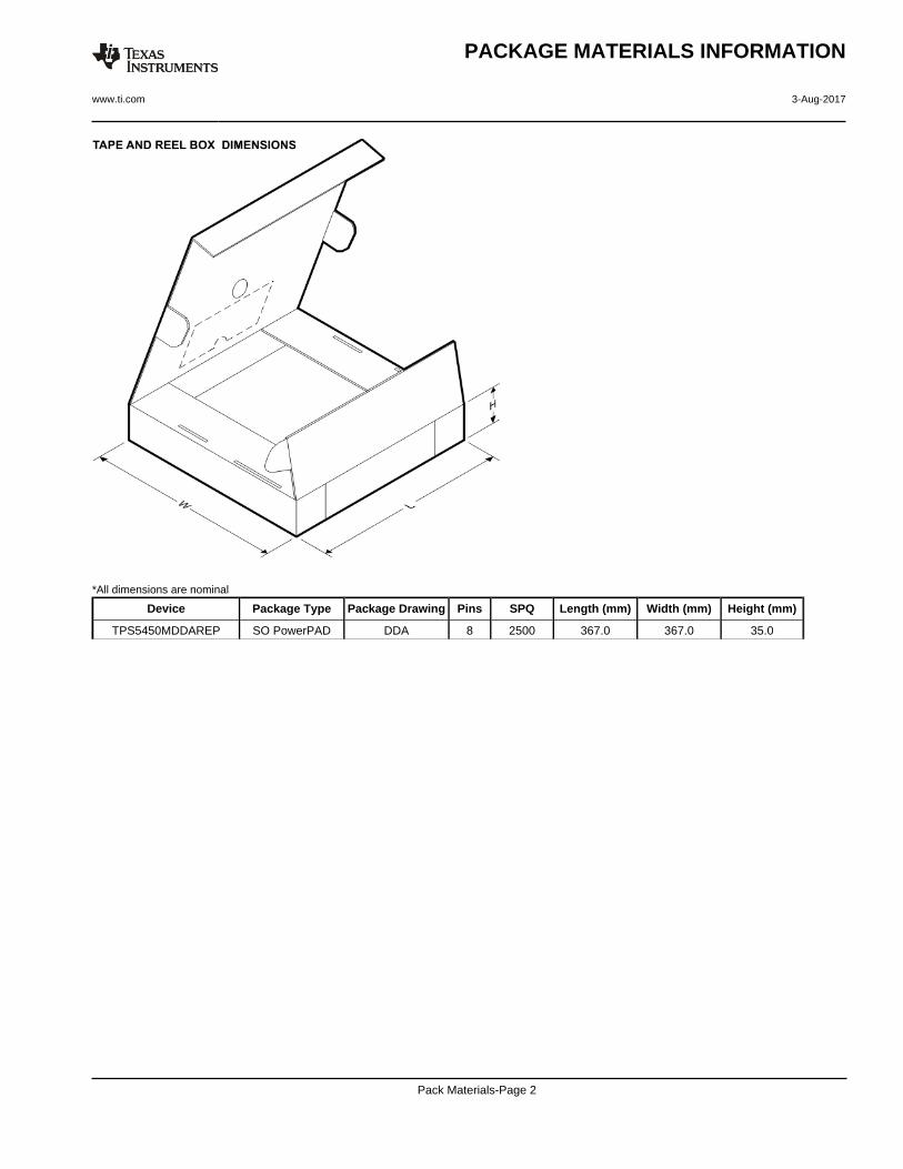
TPS5450MDDAREP SO PowerPAD DDA 8 2500 367.0 367.0 35.0
PACKAGE MATERIALS INFORMATION
www.ti.com 3-Aug-2017
Pack Materials-Page 2
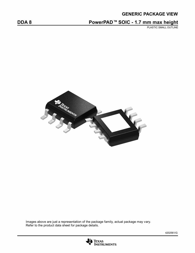
GENERIC PACKAGE VIEW
Images above are just a representation of the package family, actual package may vary.Refer to the product data sheet for package details.
DDA 8 PowerPAD TM SOIC - 1.7 mm max heightPLASTIC SMALL OUTLINE
4202561/G
www.ti.com
PACKAGE OUTLINE
C TYP6.2
5.8
1.7 MAX
6X 1.27
8X 0.510.31
2X3.81
TYP0.250.10
0 - 80.150.00
2.62.0
3.12.5
0.25GAGE PLANE
1.270.40
A
NOTE 3
5.04.8
B 4.03.8
4221637/B 03/2016
PowerPAD SOIC - 1.7 mm max heightDDA0008JPLASTIC SMALL OUTLINE
NOTES: 1. All linear dimensions are in millimeters. Any dimensions in parenthesis are for reference only. Dimensioning and tolerancing per ASME Y14.5M. 2. This drawing is subject to change without notice. 3. This dimension does not include mold flash, protrusions, or gate burrs. Mold flash, protrusions, or gate burrs shall not exceed 0.15 mm per side. 4. This dimension does not include interlead flash. Interlead flash shall not exceed 0.25 mm per side.5. Reference JEDEC registration MS-012, variation BA.
PowerPAD is a trademark of Texas Instruments.
TM
18
0.1 C A B
54
PIN 1 IDAREA
NOTE 4
SEATING PLANE
0.1 C
SEE DETAIL A
DETAIL ATYPICAL
SCALE 2.400
EXPOSEDTHERMAL PAD
4
1
5
8
www.ti.com
EXAMPLE BOARD LAYOUT
(5.4)
0.07 MAXALL AROUND
0.07 MINALL AROUND
8X (1.55)
8X (0.6)
6X (1.27)
(2.95)NOTE 9
(4.9)NOTE 9
(2.6)
(3.1)SOLDER MASK
OPENING
( ) TYPVIA
0.2
(1.3) TYP
(1.3)TYP
4221637/B 03/2016
PowerPAD SOIC - 1.7 mm max heightDDA0008JPLASTIC SMALL OUTLINE
SYMM
SYMM
SEE DETAILS
LAND PATTERN EXAMPLESCALE:10X
1
4 5
8
SOLDER MASKOPENING
METAL COVEREDBY SOLDER MASK
SOLDER MASKDEFINED PAD
NOTES: (continued) 6. Publication IPC-7351 may have alternate designs. 7. Solder mask tolerances between and around signal pads can vary based on board fabrication site. 8. This package is designed to be soldered to a thermal pad on the board. For more information, see Texas Instruments literature numbers SLMA002 (www.ti.com/lit/slma002) and SLMA004 (www.ti.com/lit/slma004).9. Size of metal pad may vary due to creepage requirement.
TM
METALSOLDER MASKOPENING
NON SOLDER MASKDEFINED
SOLDER MASK DETAILS
OPENINGSOLDER MASK METAL UNDER
SOLDER MASK
SOLDER MASKDEFINED
www.ti.com
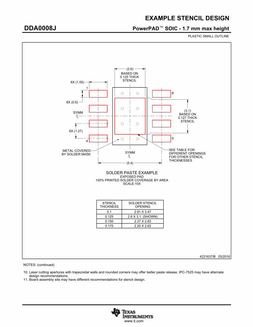
EXAMPLE STENCIL DESIGN
8X (1.55)
8X (0.6)
6X (1.27)
(5.4)
(2.6)
(3.1)BASED ON
0.127 THICKSTENCIL
4221637/B 03/2016
PowerPAD SOIC - 1.7 mm max heightDDA0008JPLASTIC SMALL OUTLINE
2.20 X 2.620.1752.37 X 2.830.150
2.6 X 3.1 (SHOWN)0.1252.91 X 3.470.1
SOLDER STENCILOPENING
STENCILTHICKNESS
NOTES: (continued) 10. Laser cutting apertures with trapezoidal walls and rounded corners may offer better paste release. IPC-7525 may have alternate design recommendations. 11. Board assembly site may have different recommendations for stencil design.
TM
SOLDER PASTE EXAMPLEEXPOSED PAD
100% PRINTED SOLDER COVERAGE BY AREASCALE:10X
SYMM
SYMM
1
45
8
BASED ON0.125 THICK
STENCIL
BY SOLDER MASKMETAL COVERED SEE TABLE FOR
DIFFERENT OPENINGSFOR OTHER STENCILTHICKNESSES
IMPORTANT NOTICE
Texas Instruments Incorporated (TI) reserves the right to make corrections, enhancements, improvements and other changes to itssemiconductor products and services per JESD46, latest issue, and to discontinue any product or service per JESD48, latest issue. Buyersshould obtain the latest relevant information before placing orders and should verify that such information is current and complete.TI’s published terms of sale for semiconductor products (http://www.ti.com/sc/docs/stdterms.htm) apply to the sale of packaged integratedcircuit products that TI has qualified and released to market. Additional terms may apply to the use or sale of other types of TI products andservices.Reproduction of significant portions of TI information in TI data sheets is permissible only if reproduction is without alteration and isaccompanied by all associated warranties, conditions, limitations, and notices. TI is not responsible or liable for such reproduceddocumentation. Information of third parties may be subject to additional restrictions. Resale of TI products or services with statementsdifferent from or beyond the parameters stated by TI for that product or service voids all express and any implied warranties for theassociated TI product or service and is an unfair and deceptive business practice. TI is not responsible or liable for any such statements.Buyers and others who are developing systems that incorporate TI products (collectively, “Designers”) understand and agree that Designersremain responsible for using their independent analysis, evaluation and judgment in designing their applications and that Designers havefull and exclusive responsibility to assure the safety of Designers' applications and compliance of their applications (and of all TI productsused in or for Designers’ applications) with all applicable regulations, laws and other applicable requirements. Designer represents that, withrespect to their applications, Designer has all the necessary expertise to create and implement safeguards that (1) anticipate dangerousconsequences of failures, (2) monitor failures and their consequences, and (3) lessen the likelihood of failures that might cause harm andtake appropriate actions. Designer agrees that prior to using or distributing any applications that include TI products, Designer willthoroughly test such applications and the functionality of such TI products as used in such applications.TI’s provision of technical, application or other design advice, quality characterization, reliability data or other services or information,including, but not limited to, reference designs and materials relating to evaluation modules, (collectively, “TI Resources”) are intended toassist designers who are developing applications that incorporate TI products; by downloading, accessing or using TI Resources in anyway, Designer (individually or, if Designer is acting on behalf of a company, Designer’s company) agrees to use any particular TI Resourcesolely for this purpose and subject to the terms of this Notice.TI’s provision of TI Resources does not expand or otherwise alter TI’s applicable published warranties or warranty disclaimers for TIproducts, and no additional obligations or liabilities arise from TI providing such TI Resources. TI reserves the right to make corrections,enhancements, improvements and other changes to its TI Resources. TI has not conducted any testing other than that specificallydescribed in the published documentation for a particular TI Resource.Designer is authorized to use, copy and modify any individual TI Resource only in connection with the development of applications thatinclude the TI product(s) identified in such TI Resource. NO OTHER LICENSE, EXPRESS OR IMPLIED, BY ESTOPPEL OR OTHERWISETO ANY OTHER TI INTELLECTUAL PROPERTY RIGHT, AND NO LICENSE TO ANY TECHNOLOGY OR INTELLECTUAL PROPERTYRIGHT OF TI OR ANY THIRD PARTY IS GRANTED HEREIN, including but not limited to any patent right, copyright, mask work right, orother intellectual property right relating to any combination, machine, or process in which TI products or services are used. Informationregarding or referencing third-party products or services does not constitute a license to use such products or services, or a warranty orendorsement thereof. Use of TI Resources may require a license from a third party under the patents or other intellectual property of thethird party, or a license from TI under the patents or other intellectual property of TI.TI RESOURCES ARE PROVIDED “AS IS” AND WITH ALL FAULTS. TI DISCLAIMS ALL OTHER WARRANTIES ORREPRESENTATIONS, EXPRESS OR IMPLIED, REGARDING RESOURCES OR USE THEREOF, INCLUDING BUT NOT LIMITED TOACCURACY OR COMPLETENESS, TITLE, ANY EPIDEMIC FAILURE WARRANTY AND ANY IMPLIED WARRANTIES OFMERCHANTABILITY, FITNESS FOR A PARTICULAR PURPOSE, AND NON-INFRINGEMENT OF ANY THIRD PARTY INTELLECTUALPROPERTY RIGHTS. TI SHALL NOT BE LIABLE FOR AND SHALL NOT DEFEND OR INDEMNIFY DESIGNER AGAINST ANY CLAIM,INCLUDING BUT NOT LIMITED TO ANY INFRINGEMENT CLAIM THAT RELATES TO OR IS BASED ON ANY COMBINATION OFPRODUCTS EVEN IF DESCRIBED IN TI RESOURCES OR OTHERWISE. IN NO EVENT SHALL TI BE LIABLE FOR ANY ACTUAL,DIRECT, SPECIAL, COLLATERAL, INDIRECT, PUNITIVE, INCIDENTAL, CONSEQUENTIAL OR EXEMPLARY DAMAGES INCONNECTION WITH OR ARISING OUT OF TI RESOURCES OR USE THEREOF, AND REGARDLESS OF WHETHER TI HAS BEENADVISED OF THE POSSIBILITY OF SUCH DAMAGES.Unless TI has explicitly designated an individual product as meeting the requirements of a particular industry standard (e.g., ISO/TS 16949and ISO 26262), TI is not responsible for any failure to meet such industry standard requirements.Where TI specifically promotes products as facilitating functional safety or as compliant with industry functional safety standards, suchproducts are intended to help enable customers to design and create their own applications that meet applicable functional safety standardsand requirements. Using products in an application does not by itself establish any safety features in the application. Designers mustensure compliance with safety-related requirements and standards applicable to their applications. Designer may not use any TI products inlife-critical medical equipment unless authorized officers of the parties have executed a special contract specifically governing such use.Life-critical medical equipment is medical equipment where failure of such equipment would cause serious bodily injury or death (e.g., lifesupport, pacemakers, defibrillators, heart pumps, neurostimulators, and implantables). Such equipment includes, without limitation, allmedical devices identified by the U.S. Food and Drug Administration as Class III devices and equivalent classifications outside the U.S.TI may expressly designate certain products as completing a particular qualification (e.g., Q100, Military Grade, or Enhanced Product).Designers agree that it has the necessary expertise to select the product with the appropriate qualification designation for their applicationsand that proper product selection is at Designers’ own risk. Designers are solely responsible for compliance with all legal and regulatoryrequirements in connection with such selection.Designer will fully indemnify TI and its representatives against any damages, costs, losses, and/or liabilities arising out of Designer’s non-compliance with the terms and provisions of this Notice.


![SWIFT Fidelity Integrity Assessment (SWIFT-FIA)swiftschools.org/sites/default/files/SWIFT_FIA_1 3... · SWIFT Fidelity Integrity Assessment [SWIFT-FIA] v.1.3 for SWIFT Partner Schools](https://static.documents.pub/doc/80x56/604484a45d3f270b4e56b476/swift-fidelity-integrity-assessment-swift-fia-3-swift-fidelity-integrity.jpg)


