AND MEDICAL APPLICATIONS• Adaptive Delay Set• Controlled Baseline• Bidirectional Oscillator Synchronization• One Assembly/Test Site• Capability for Voltage-Mode or Current-Mode• One Fabrication SiteControl• Available in Military (–55°C/125°C)• Programmable Soft Start/Soft Stop and Chip
Temperature Range (1)Disable Via a Single Pin
• Extended Product Life Cycle• 0% to 100% Duty-Cycle Control
• Product Traceability• Operation to 1 MHz• Low Active Current Consumption (5 mA Typ at
500 kHz)• Very Low Current Consumption During
Undervoltage Lock Out (150 μA Typ)
(1) Additional temperature ranges available - contact factory
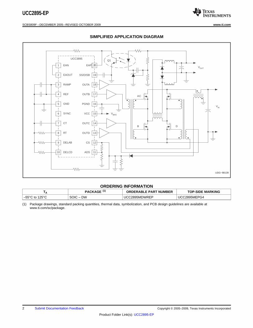
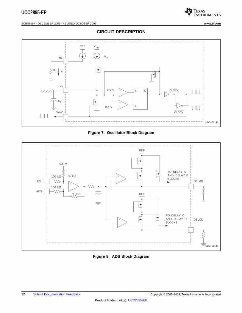
DESCRIPTIONThe UCC2895-EP is a phase-shift pulse-width modulation (PWM) controller that implements control of afull-bridge power stage by phase shifting the switching of one half bridge with respect to the other. It allowsconstant frequency PWM in conjunction with resonant zero-voltage switching to provide high efficiency at highfrequencies. The device can be used either as a voltage-mode or current-mode controller.
While the UCC2895-EP maintains the functionality of the UC2875/6/7/8 family, it improves on that controllerfamily with additional features, such as enhanced control logic, adaptive delay set, and shutdown capability.Since the device is built in BCDMOS, it operates with dramatically less supply current than its bipolarcounterparts. The UCC2895-EP can operate with a maximum clock frequency of 1 MHz.
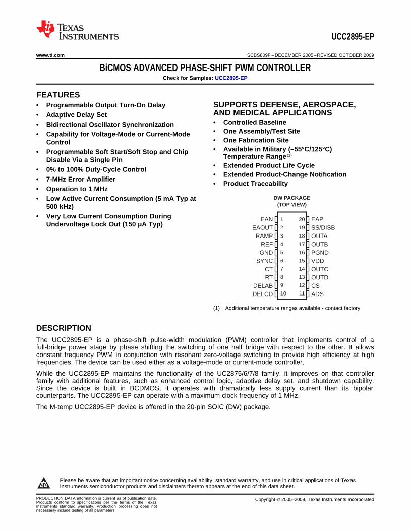
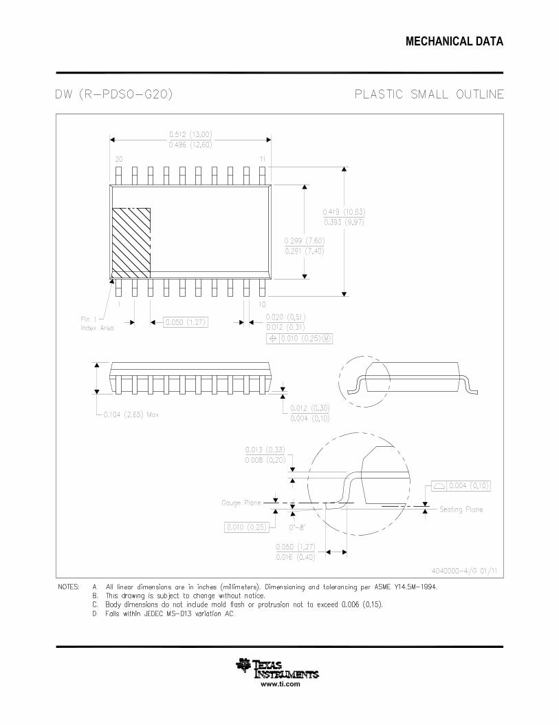
The M-temp UCC2895-EP device is offered in the 20-pin SOIC (DW) package.
1
Please be aware that an important notice concerning availability, standard warranty, and use in critical applications of TexasInstruments semiconductor products and disclaimers thereto appears at the end of this data sheet.
www.ti.com SCBS809F –DECEMBER 2005–REVISED OCTOBER 2009
Table 1. PIN DESCRIPTION
NAME DESCRIPTION
Adaptive delay set.This function sets the ratio between the maximum and minimum programmed output delay deadtime. When ADS is connected directly to CS, no delay modulation occurs. Maximum delay modulation occurs whenADS is grounded. In this case, delay time is four times longer when CS = 0 than when CS = 2 V (the peak currentthreshold). ADS changes the output voltage on the delay (DELAB and DELCD) pins by:
ADS
where VCS and VADS are in volts. ADS must be limited to between 0 V and 2.5 V and must be less than, or equalto, CS. DELAB and DELCD also are clamped to a minimum of 0.5 V.
Current sense. CS is the inverting input of the current-sense comparator, and the noninverting input of theovercurrent comparator and the ADS amplifier. The CS signal is used for cycle-by-cycle current limiting in peakCS current-mode control and for overcurrent protection in all cases with a secondary threshold for output shutdown. Anoutput disable initiated by an overcurrent fault also results in a restart cycle, called soft stop, with full soft start.
Oscillator timing capacitor (see Figure 3). The UCC2895-EP oscillator charges CT via a programmed current. Thewaveform on CT is a sawtooth, with a peak voltage of 2.35 V. The approximate oscillator period is calculated by:
CT
where CT is in farads, RT is in ohms, and tOSC is in seconds. CT can range from 100 pF to 880 pF. Note that alarge CT and a small RT combination results in extended fall times on the CT waveform. The increased fall timeincreases the SYNC pulse width, thus, limiting the maximum phase shift between OUTA/ OUTB and OUTC/ OUTDoutputs, which limits the maximum duty cycle of the converter.
Delay programming between complementary outputs. DELAB programs the dead time between switching of OUTAand OUTB, and DELCD programs the dead time between OUTC and OUTD. This delay is introduced betweencomplementary outputs in the same leg of the external bridge. The UCC2895-EP allows the user to select the delayin which the resonant switching of the external power stages takes place. Separate delays are provided for the twohalf bridges to accommodate differences in resonant capacitor charging currents. The delay in each stage is setaccording to the formula:
DELAB, DELCD
where VDEL is in volts, RDEL is in ohms, and tDELAY is in seconds. DELAB and DELCD can source approximately1 mA maximum. Delay resistors must be chosen so that this maximum is not exceeded. Programmable outputdelay can be defeated by tying DELAB and/or DELCD to REF. For optimum performance, keep stray capacitanceon these pins at <10 pF.
EAN Error amplifier negative. Inverting input to the error amplifier. Keep below 3.6 V for proper operation.
Error amplifier output. EAOUT also is connected internally to the noninverting input of the PWM comparator and theno-load comparator. EAOUT is internally clamped to the soft-start voltage. The no-load comparator shuts down theEAOUT output stages when EAOUT falls below 500 mV and allows the outputs to turn on again when EAOUT rises above600 mV.
EAP Error amplifier positive. Noninverting input to the error amplifier. Keep below 3.6 V for proper operation.
GND Ground. Chip ground for all circuits except the output stages.
Outputs. These outputs are 100-mA complementary MOS drivers and are optimized to drive FET driver circuits.OUTA and OUTB are fully complementary (assuming no programmed delay). They operate near 50% duty cycleOUTA and one-half the oscillating frequency. OUTA and OUTB are intended to drive one half-bridge circuit in an externalOUTB power stage. OUTC and OUTD drive the other half bridge and have the same characteristics as OUTA and OUTB.OUTC OUTC is phase shifted with respect to OUTA, and OUTD is phase shifted with respect to OUTB. Note thatOUTD changing the phase relationship of OUTC and OUTD, with respect to OUTA and OUTB, requires other than thenominal 50% duty ratio on OUTC and OUTD during those transients
Output stage ground. To keep output switching noise from critical analog circuits, the UCC2895-EP has twodifferent ground connections. PGND is the ground connection for the high-current output stages. Both GND andPGND PGND must be electrically tied together closely near the IC. Also, since PGND carries high current, board tracesmust be low impedance.
Inverting input of PWM comparator. RAMP receives either the CT waveform in voltage and average current-modeRAMP controls, or the current signal (plus slope compensation) in peak current-mode control. An internal discharge
transistor is provided on RAMP, which is triggered during the oscillator dead time.
SCBS809F –DECEMBER 2005–REVISED OCTOBER 2009 www.ti.com
Table 1. PIN DESCRIPTION (continued)
NAME DESCRIPTION
Oscillator timing resistor (see Figure 3). The oscillator in the UCC2895-EP operates by charging an external timingcapacitor, CT, with a fixed current programmed by RT. RT current is calculated as:
RT
RT can range from 40 kΩ to 120 kΩ. Soft-start charging and discharging current also are programmed by IRT.
5 V ± 1.2% voltage reference. REF supplies power to internal circuitry, and also can supply up to 5 mA to externalREF loads. The reference is shut down during undervoltage lockout, but is operational during all other disable modes.
For best performance, bypass with a 0.1-μF low ESR, low ESL capacitor to ground. Do not use more than 1.0 μF.
Soft start/disable. SS/DISB combines two independent functions:• Disable mode. A rapid shutdown of the chip is accomplished by any one of the following: externally forcing
SS/DISB below 0.5 V, externally forcing REF below 4 V, VDD dropping below the UVLO threshold, or anovercurrent fault is sensed (CS = 2.5 V).In the case of REF pulled below 4 V or an UVLO condition, SS/DISB actively is pulled to ground via an internalMOSFET switch. If an overcurrent is sensed, SS/DISB sinks a current of 10 × IRT until SS/DISB falls below0.5 V.
SS/DISB Note that, if SS/DISB is externally forced below 0.5 V, the pin starts to source current equal to IRT. Also notethat the only time the part switches into the low IDD current mode is when the part is in undervoltage lockout.
• Soft-start mode. After a fault or disable condition has passed and VDD is above the start threshold and/orSS/DISB falls below 0.5 V during a soft stop, SS/DISB switches to a soft-start mode. The pin now sourcescurrent equal to IRT. A user-selected capacitor on SS/DISB determines the soft start and soft-start time. Inaddition, a resistor in parallel with the capacitor may be used, limiting the maximum voltage on SS/DISB. Notethat SS/DISB actively clamps the EAOUT voltage to approximately the SS/DISB voltage during both soft-start,soft-stop, and disable conditions.
Synchronization (see Figure 3). SYNC is bidirectional. When used as an output, SYNC can be used as a clock,which is the same as the chip’s internal clock. When used as an input, SYNC overrides the chip’s internal oscillatorand acts as its clock signal. This bidirectional feature allows synchronization of multiple power supplies. SYNC alsoSYNC internally discharges the CT capacitor and any filter capacitors that are present on RAMP. The internal SYNCcircuitry is level sensitive, with an input low threshold of 1.9 V and an input high threshold of 2.1 V. A resistor assmall as 3.9 kΩ may be tied between SYNC and GND to reduce the synchronization pulse width.
VDD Power supply. VDD must be bypassed with a minimum of a 1.0-μF low ESR, low ESL capacitor to ground.
Absolute Maximum Ratings (1) (2)
over operating free-air temperature range (unless otherwise noted)MIN MAX UNIT
N package 1 WPower dissipation(at TA = 25°C) DW package 650 mW
Tstg Storage temperature range –65 150 °C
TJ Junction temperature range –55 150 °C
Lead temperature Soldering, 10 s 300 °C
(1) Stresses beyond those listed under "absolute maximum ratings" may cause permanent damage to the device. These are stress ratingsonly, and functional operation of the device at these or any other conditions beyond those indicated under "recommended operatingconditions" is not implied. Exposure to absolute-maximum-rated conditions for extended periods may affect device reliability.
(2) Currents are positive into and negative out of the specified terminal.
(1) It is recommended that there be a single point grounded between GND and PGND directly under the device. There should be aseperate ground plane associated with the GND pin and all components associated with pins 1 through 12 plus 19 and 20 be locatedover this ground plane. Any connections associated with these pins to ground should be connected to this ground plane.
(2) The VDD capacitor should be a low ESR, ESL ceramic capacitor located directly across the VDD and PGND pins. A larger bulk capacitorshould belocated as physically close as possible to the VDD pins.
(3) The VREF capacitor should be a low ESR, ESL ceramic capacitor located directly across the REF and GND pins. If a larger capacitor isdesired for the VREF then it should be located near the VREF capacitor and connected to the VREF pin with a resistor of 51 Ω or greater.The bulk capacitor on VDD must be a factor of 10 greater than the total VREF capacitance.
(4) It is not recommended that the device operate under conditions beyond those specified in this table for extended periods of time.
ADS bias current 0 V < ADS < 2.5 V, 0 V < CS < 2.5 V –20 20 μA
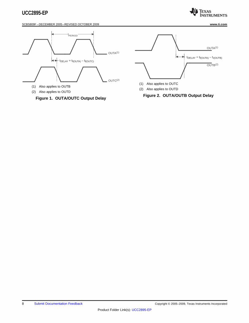
(2) Minimum phase shift is defined as:
where:tf(OUTA) = falling edge of OUTA signaltf(OUTB) = falling edge of OUTB signaltf(OUTC) = falling edge of OUTC signaltf(OUTD) = falling edge of OUTD signalt(PERIOD) = period of OUTA or OUTB signal
(3) Output delay is measured between OUTA/OUTB or OUTC/OUTD. Output delay is shown in Figure 1 and Figure 2 , where:tf(OUTA) = falling edge of OUTA signaltr(OUTB) = rising edge of OUTB signal
www.ti.com SCBS809F –DECEMBER 2005–REVISED OCTOBER 2009
APPLICATION INFORMATION
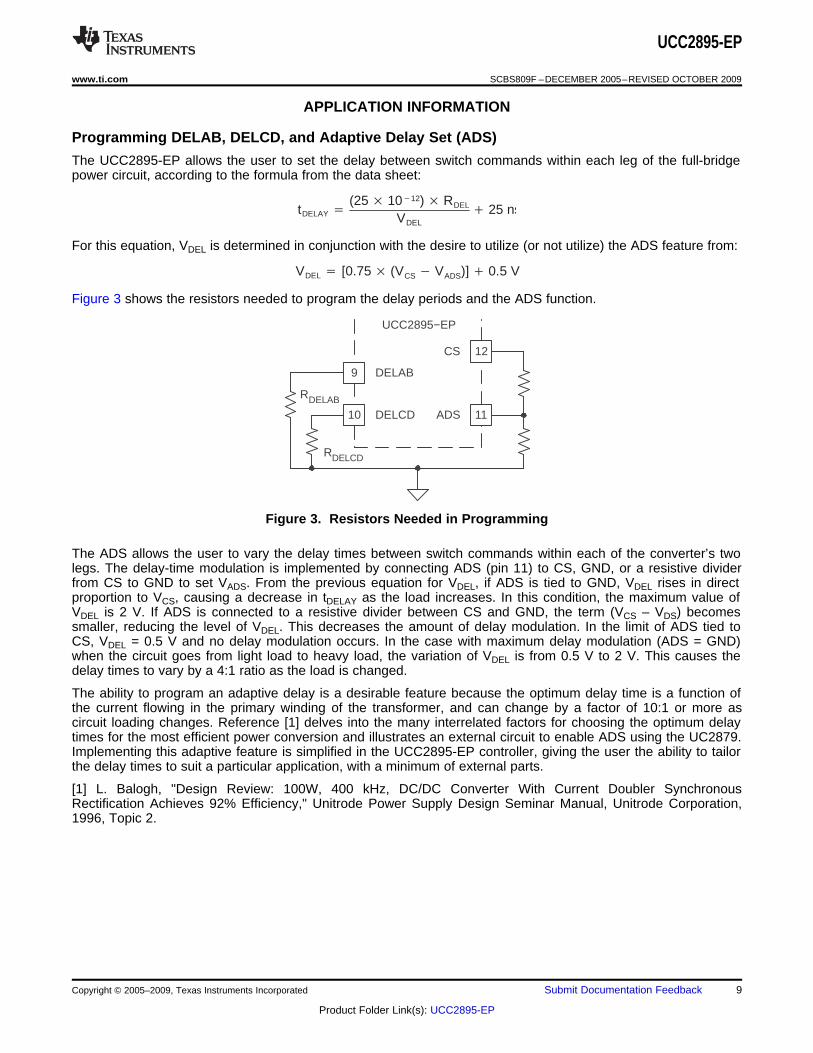
Programming DELAB, DELCD, and Adaptive Delay Set (ADS)
The UCC2895-EP allows the user to set the delay between switch commands within each leg of the full-bridgepower circuit, according to the formula from the data sheet:
For this equation, VDEL is determined in conjunction with the desire to utilize (or not utilize) the ADS feature from:
Figure 3 shows the resistors needed to program the delay periods and the ADS function.
Figure 3. Resistors Needed in Programming
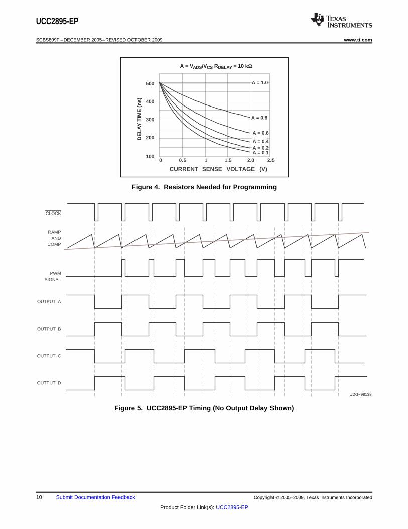
The ADS allows the user to vary the delay times between switch commands within each of the converter’s twolegs. The delay-time modulation is implemented by connecting ADS (pin 11) to CS, GND, or a resistive dividerfrom CS to GND to set VADS. From the previous equation for VDEL, if ADS is tied to GND, VDEL rises in directproportion to VCS, causing a decrease in tDELAY as the load increases. In this condition, the maximum value ofVDEL is 2 V. If ADS is connected to a resistive divider between CS and GND, the term (VCS – VDS) becomessmaller, reducing the level of VDEL. This decreases the amount of delay modulation. In the limit of ADS tied toCS, VDEL = 0.5 V and no delay modulation occurs. In the case with maximum delay modulation (ADS = GND)when the circuit goes from light load to heavy load, the variation of VDEL is from 0.5 V to 2 V. This causes thedelay times to vary by a 4:1 ratio as the load is changed.
The ability to program an adaptive delay is a desirable feature because the optimum delay time is a function ofthe current flowing in the primary winding of the transformer, and can change by a factor of 10:1 or more ascircuit loading changes. Reference [1] delves into the many interrelated factors for choosing the optimum delaytimes for the most efficient power conversion and illustrates an external circuit to enable ADS using the UC2879.Implementing this adaptive feature is simplified in the UCC2895-EP controller, giving the user the ability to tailorthe delay times to suit a particular application, with a minimum of external parts.
[1] L. Balogh, "Design Review: 100W, 400 kHz, DC/DC Converter With Current Doubler SynchronousRectification Achieves 92% Efficiency," Unitrode Power Supply Design Seminar Manual, Unitrode Corporation,1996, Topic 2.
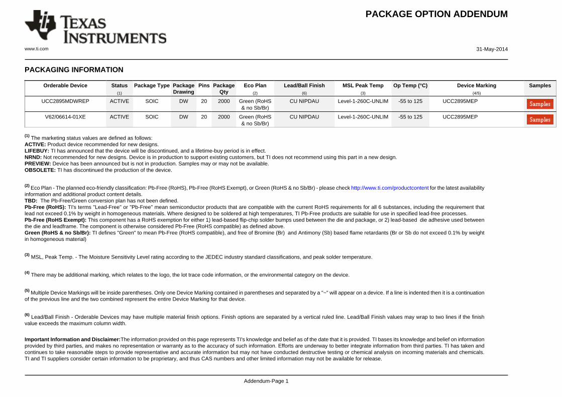
UCC2895MDWREP ACTIVE SOIC DW 20 2000 Green (RoHS& no Sb/Br)
CU NIPDAU Level-1-260C-UNLIM -55 to 125 UCC2895MEP
V62/06614-01XE ACTIVE SOIC DW 20 2000 Green (RoHS& no Sb/Br)
CU NIPDAU Level-1-260C-UNLIM -55 to 125 UCC2895MEP
(1) The marketing status values are defined as follows:ACTIVE: Product device recommended for new designs.LIFEBUY: TI has announced that the device will be discontinued, and a lifetime-buy period is in effect.NRND: Not recommended for new designs. Device is in production to support existing customers, but TI does not recommend using this part in a new design.PREVIEW: Device has been announced but is not in production. Samples may or may not be available.OBSOLETE: TI has discontinued the production of the device.
(2) Eco Plan - The planned eco-friendly classification: Pb-Free (RoHS), Pb-Free (RoHS Exempt), or Green (RoHS & no Sb/Br) - please check http://www.ti.com/productcontent for the latest availabilityinformation and additional product content details.TBD: The Pb-Free/Green conversion plan has not been defined.Pb-Free (RoHS): TI's terms "Lead-Free" or "Pb-Free" mean semiconductor products that are compatible with the current RoHS requirements for all 6 substances, including the requirement thatlead not exceed 0.1% by weight in homogeneous materials. Where designed to be soldered at high temperatures, TI Pb-Free products are suitable for use in specified lead-free processes.Pb-Free (RoHS Exempt): This component has a RoHS exemption for either 1) lead-based flip-chip solder bumps used between the die and package, or 2) lead-based die adhesive used betweenthe die and leadframe. The component is otherwise considered Pb-Free (RoHS compatible) as defined above.Green (RoHS & no Sb/Br): TI defines "Green" to mean Pb-Free (RoHS compatible), and free of Bromine (Br) and Antimony (Sb) based flame retardants (Br or Sb do not exceed 0.1% by weightin homogeneous material)
(3) MSL, Peak Temp. - The Moisture Sensitivity Level rating according to the JEDEC industry standard classifications, and peak solder temperature.
(4) There may be additional marking, which relates to the logo, the lot trace code information, or the environmental category on the device.
(5) Multiple Device Markings will be inside parentheses. Only one Device Marking contained in parentheses and separated by a "~" will appear on a device. If a line is indented then it is a continuationof the previous line and the two combined represent the entire Device Marking for that device.
(6) Lead/Ball Finish - Orderable Devices may have multiple material finish options. Finish options are separated by a vertical ruled line. Lead/Ball Finish values may wrap to two lines if the finishvalue exceeds the maximum column width.
Important Information and Disclaimer:The information provided on this page represents TI's knowledge and belief as of the date that it is provided. TI bases its knowledge and belief on informationprovided by third parties, and makes no representation or warranty as to the accuracy of such information. Efforts are underway to better integrate information from third parties. TI has taken andcontinues to take reasonable steps to provide representative and accurate information but may not have conducted destructive testing or chemical analysis on incoming materials and chemicals.TI and TI suppliers consider certain information to be proprietary, and thus CAS numbers and other limited information may not be available for release.
In no event shall TI's liability arising out of such information exceed the total purchase price of the TI part(s) at issue in this document sold by TI to Customer on an annual basis.
OTHER QUALIFIED VERSIONS OF UCC2895-EP :
• Catalog: UCC2895
• Automotive: UCC2895-Q1
NOTE: Qualified Version Definitions:
• Catalog - TI's standard catalog product
• Automotive - Q100 devices qualified for high-reliability automotive applications targeting zero defects
IMPORTANT NOTICETexas Instruments Incorporated and its subsidiaries (TI) reserve the right to make corrections, enhancements, improvements and otherchanges to its semiconductor products and services per JESD46, latest issue, and to discontinue any product or service per JESD48, latestissue. Buyers should obtain the latest relevant information before placing orders and should verify that such information is current andcomplete. All semiconductor products (also referred to herein as “components”) are sold subject to TI’s terms and conditions of salesupplied at the time of order acknowledgment.TI warrants performance of its components to the specifications applicable at the time of sale, in accordance with the warranty in TI’s termsand conditions of sale of semiconductor products. Testing and other quality control techniques are used to the extent TI deems necessaryto support this warranty. Except where mandated by applicable law, testing of all parameters of each component is not necessarilyperformed.TI assumes no liability for applications assistance or the design of Buyers’ products. Buyers are responsible for their products andapplications using TI components. To minimize the risks associated with Buyers’ products and applications, Buyers should provideadequate design and operating safeguards.TI does not warrant or represent that any license, either express or implied, is granted under any patent right, copyright, mask work right, orother intellectual property right relating to any combination, machine, or process in which TI components or services are used. Informationpublished by TI regarding third-party products or services does not constitute a license to use such products or services or a warranty orendorsement thereof. Use of such information may require a license from a third party under the patents or other intellectual property of thethird party, or a license from TI under the patents or other intellectual property of TI.Reproduction of significant portions of TI information in TI data books or data sheets is permissible only if reproduction is without alterationand is accompanied by all associated warranties, conditions, limitations, and notices. TI is not responsible or liable for such altereddocumentation. Information of third parties may be subject to additional restrictions.Resale of TI components or services with statements different from or beyond the parameters stated by TI for that component or servicevoids all express and any implied warranties for the associated TI component or service and is an unfair and deceptive business practice.TI is not responsible or liable for any such statements.Buyer acknowledges and agrees that it is solely responsible for compliance with all legal, regulatory and safety-related requirementsconcerning its products, and any use of TI components in its applications, notwithstanding any applications-related information or supportthat may be provided by TI. Buyer represents and agrees that it has all the necessary expertise to create and implement safeguards whichanticipate dangerous consequences of failures, monitor failures and their consequences, lessen the likelihood of failures that might causeharm and take appropriate remedial actions. Buyer will fully indemnify TI and its representatives against any damages arising out of the useof any TI components in safety-critical applications.In some cases, TI components may be promoted specifically to facilitate safety-related applications. With such components, TI’s goal is tohelp enable customers to design and create their own end-product solutions that meet applicable functional safety standards andrequirements. Nonetheless, such components are subject to these terms.No TI components are authorized for use in FDA Class III (or similar life-critical medical equipment) unless authorized officers of the partieshave executed a special agreement specifically governing such use.Only those TI components which TI has specifically designated as military grade or “enhanced plastic” are designed and intended for use inmilitary/aerospace applications or environments. Buyer acknowledges and agrees that any military or aerospace use of TI componentswhich have not been so designated is solely at the Buyer's risk, and that Buyer is solely responsible for compliance with all legal andregulatory requirements in connection with such use.TI has specifically designated certain components as meeting ISO/TS16949 requirements, mainly for automotive use. In any case of use ofnon-designated products, TI will not be responsible for any failure to meet ISO/TS16949.Products ApplicationsAudio www.ti.com/audio Automotive and Transportation www.ti.com/automotiveAmplifiers amplifier.ti.com Communications and Telecom www.ti.com/communicationsData Converters dataconverter.ti.com Computers and Peripherals www.ti.com/computersDLP® Products www.dlp.com Consumer Electronics www.ti.com/consumer-appsDSP dsp.ti.com Energy and Lighting www.ti.com/energyClocks and Timers www.ti.com/clocks Industrial www.ti.com/industrialInterface interface.ti.com Medical www.ti.com/medicalLogic logic.ti.com Security www.ti.com/securityPower Mgmt power.ti.com Space, Avionics and Defense www.ti.com/space-avionics-defenseMicrocontrollers microcontroller.ti.com Video and Imaging www.ti.com/videoRFID www.ti-rfid.comOMAP Applications Processors www.ti.com/omap TI E2E Community e2e.ti.comWireless Connectivity www.ti.com/wirelessconnectivity