Jennie S. HwangH–Technologies Group, Inc.Cleveland, Ohio
5.1 Introduction
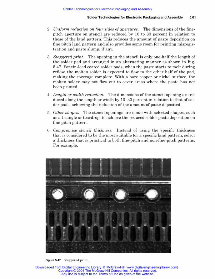
5.1.1 Scope
What drives the end-use market are the continued convergence of computing,communication, and entertainment as well as the relentless growth of thewireless, portable, handheld digital electronics and optoelectronics. On theever-changing technology landscape, the industry has responded and will con-tinue to respond to competitive demands in the global marketplace. New elec-tronic gadgets will be featured with increasingly higher functionality, furthersimplicity, lower cost, and greater operational ease. What has transpired fromthese market demands is continued technological innovation and an ever-shortening product life cycle. Environment-friendly manufacturing and thedelivery of environmentally benign end-use products that are ultimately safeat the end of the product life cycle will become essential to technology-busi-ness competitiveness. This is a continuing challenge to the industry. Solderhas served as the interconnecting material for all three levels of connections:die, package, and board assembly. In addition, tin/lead solder is commonlyused as a surface coating for component leads and PCB surface finishes. In ad-dition to solder materials, the process used to form solder joints to accomplishthe vital function of electrical, thermal, and mechanical linkages between twometallic surfaces is equally important.
Source: Electronic Materials and Processes Handbook
Any use is subject to the Terms of Use as given at the website.
5.2 Chapter 5
This chapter addresses solder technologies in both material and process as-pects for electronic packaging and assembly. Considering the established roleof lead (Pb) and the demand in Pb-free materials, solder can be classified as ei-ther lead-containing or lead-free. In light of the global environmental commit-ment, this chapter will also cover Pb-free materials in terms of theirproperties and characteristics that are important to their applications in elec-tronic packaging and assembly.
5.1.2 Surface mount technology
In this electronic and information age, we witness new technology develop-ments and new product introductions to the marketplace almost on a monthlybasis. One of the strongest trends, however, in the electronics interconnectionand packaging segment is utilization of the surface-mounting concept to de-velop superior circuit board assemblies in both performance and cost. Thisconcept has been utilized in hybrid assembly since the 1960s by interconnect-ing chip resistors, chip capacitors, and bare semiconductor dies on metallizedsubstrates. Nevertheless, the potential of surface mounting was not fully ex-plored and utilized until the early 1980s.
What is surface-mount technology? As the name implies, it is basically theapplication of science and engineering principles to board-level assembly byplacing components and devices on the surface of the printed circuit board in-stead of through the board. Although this concept appears to be straightfor-ward, the impact on the production floor is enormous, not only on componentsand design but also on materials and equipment. It also narrows the distinc-tion between hybrid circuit assembly and printed circuit assembly. The specificbenefits of surface mount technology in relation to through-hole technology in-clude
Increased circuit density Decreased component size Decreased board size Reduced weight Shorter leads Shorter interconnection Improved electrical performance Facilitated automation Lower costs in volume production
5.1.3 Industry trends
5.1.3.1 Semiconductors. Looking at the hierarchy of electronics, semiconductordevices have continuously exhibited improved reliability, reduced feature size,
Solder Technologies for Electronic Packaging and Assembly
Any use is subject to the Terms of Use as given at the website.
Solder Technologies for Electronic Packaging and Assembly 5.3
increased wafer size, and doubled complexity every 18 months, in accordancewith the Moore’s law. As examples, wafer size increased from 3 to 4 in (75 to100 mm) in the 1980s to 12 in (300 mm) this year; circuits have shrunk to sub-micrometer (0.1 to 0.25 µm) from several micrometers; IC pin count has in-creased from 40 to 80 to more than hundreds or tens of hundreds; ICfabrication techniques and equipment are developing in rapid pace from wetprocess and microanalysis to X-ray lithography and nanoanalysis.
At 45 years old, integrated circuits (ICs) are moving into another era of ma-jor developments. The new copper interconnect technology facilitates the im-plementation of deep submicron circuitry thus alleviating the RC delayproblem. Copper has a significantly better conductivity than aluminum, whichhas been the backbone of IC circuits (Cu = 1.7 µΩ-cm; Al = 3.1 µΩ-cm). Copperis also known to have better electromigration resistance than aluminum.However, copper diffusion into silicon has been one of the major obstacles tothe use of copper interconnect. Using IBM’s proprietary barrier layer to pre-vent copper diffusion along with other companion technologies, the copper in-terconnect has become increasingly prevalent since 1999. IBM’s Cu-connectASIC technology (SA-12) also demonstrated 40 percent power savings by us-ing 1.8 V rather than 2.5 V. The reduction in power consumption without sac-rificing signal-to-noise quality is critical to the performance of portableelectronics.
For example, it is reported that interconnects account for more than 70 per-cent of the signal delay in a 0.25-µm chip. Interconnect RC delay increases asthe square of the minimum feature size, thus determining the IC chip perfor-mance. As the feature size continues to shrink to 0.13 µm or finer, RC delay is-sues become more critical.
In addition to the lower resistance offered by copper, a capacitance dielectricmaterial lower than SiO2 is equally important to keep the interconnect RC de-lay in control for the nanoelectronics era. System-on-a-chip is another ongoingdevelopment. Fundamentally, the material innovations will be paramount tofuture generations of IC circuits. Combining deeper understanding in materi-als science with technology development, silicon crystals will get closer to per-fection. Perfect silicon, obtained by eliminating crystal defects such asvacancies and dislocations, offers a new level of performance. Other silicontechnologies continue to advance. IBM’s strained silicon technology is re-ported to increases chip speed up to 35 percent while reducing power con-sumption without needing to shrink silicon circuits. The new strained silicontechnology speeds the flow of electrons through transistors by stretching thematerial. The stretching concept may not be new, but the know-how to manu-facture chips from this concept is a breakthrough. The process may seem sim-ple enough, like stretching fabric, but the novelty is at the atomic level whereone manipulates the atoms in silicon.
Up to now, electrons have been the workhorses for the electronic age and in-formation era, making possible all modern products from ovens and camerasto computers and cell phones. Future technology may not only be derived fromthe conventional material theories of circuits, based on the mobility and con-ductivity of electrons and phonons, but also from photons. Nonetheless, elec-
Solder Technologies for Electronic Packaging and Assembly
Any use is subject to the Terms of Use as given at the website.
5.4 Chapter 5
tron transport will remain the main power behind future products in theforeseeable future.
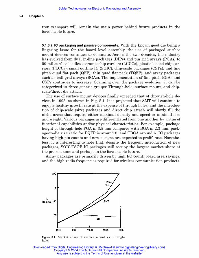
5.1.3.2 IC packaging and passive components. With the known good die being alingering issue for the board level assembly, the use of packaged surfacemount devices continues to dominate. Across the two decades, the industryhas evolved from dual in-line packages (DIPs) and pin grid arrays (PGAs) to50-mil surface leadless ceramic chip carriers (LCCCs), plastic leaded chip car-riers (PLCCs), small outline IC (SOIC), chip-scale packages (CSPs), and finepitch quad flat pack (QFP), thin quad flat pack (TQFP), and array packagessuch as ball grid arrays (BGAs). The implementation of fine-pitch BGAs andCSPs continues to increase. Scanning over the package evolution, it can becategorized in three generic groups: Through-hole, surface mount, and chip-scale/direct die attach.
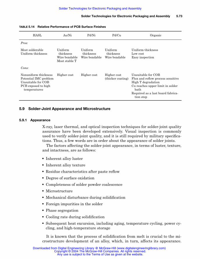
The use of surface mount devices finally exceeded that of through-hole de-vices in 1995, as shown in Fig. 5.1. It is projected that SMT will continue toenjoy a healthy growth rate at the expense of through holes, and the introduc-tion of chip-scale (size) packages and direct chip attach will slowly fill theniche areas that require either maximal density and speed or minimal sizeand weight. Various packages are differentiated from one another by virtue offunctional capabilities and/or physical characteristics. For example, packageheight of through-hole PGA in 3.5 mm compares with BGA in 2.3 mm; pack-age-to-die size ratio for PQFP is around 8, and TBGA around 5. IC packageshaving high pin counts and new designs are expected to proliferate. Nonethe-less, it is interesting to note that, despite the frequent introduction of newpackages, SOIC/TSOP IC packages still occupy the largest market share atthe present time and perhaps in the foreseeable future.
Array packages are primarily driven by high I/O count, board area savings,and the high radio frequencies required for wireless communication products.
Figure 5.1 Market share of surface mount vs. through-hole.
Solder Technologies for Electronic Packaging and Assembly
Any use is subject to the Terms of Use as given at the website.
Solder Technologies for Electronic Packaging and Assembly 5.5
The I/O pitch of BGAs generally falls in the range of 1.00 to 1.50 mm (0.040 to0.060 in). PBGA, TBGA, and CBGA all have been adopted by chip makers forthe high I/O counts required in workstations and minicomputers. Consideringall factors in performance, economics, and reliability, a 250 I/O count is consid-ered to be a break point in selecting between QFP and BGA. For products inwhich size and weight are critical to their marketability, CSP has been thecenter of attention since 1997. All six main CSP technologies (wire bond/rigidinterposer, wire bond/flex interposer, flip-chip/rigid interposer, flip-chip/flex in-terposer, lead-frame/chip on lead, and wafer-level packaging) have been put touse.
The relative size of CSPs in comparison with other SMT packages can beclearly represented by the package area/die area ratio. CSP is generally ac-cepted as less than 1.5, as opposed to BGA (1.25 mm pitch) ≅ 4, BGA (1.00 mmpitch) ≅ 2, QFP (0.4 mm pitch) ≅ 7, and QFP (0.5 mm pitch) ≅ 9.0. CSPs havemade today’s smaller portable electronics possible.
In addition to portable consumer electronics, the notebook computer is an-other application that drives the use of CSPs for relatively higher-I/O ASICchips. CSPs have also been utilized in flash memory chips and extended toDRAM and SRAM packaging. However, the requirement of high-density PCBrouting and the limited availability of package substrate materials have pre-vented the growth of high-I/O CSP technology to its fullest potential. The ma-jority of CSPs have been for low-I/O applications. While a few specific CSPdesigns have emerged as “winners,” the proliferation of new designs contin-ues. As a renewed interest, flip-chip (wherein a bare chip with solder bumpson its surface is turned upside down and bonded directly onto the substratewithout lead frame and wire bonding) has served as one of the base technolo-gies to achieve chip-size packages, although CSPs can also be accommodatedby wire bonding. As IC packages in conventional molded form or in chip size(scale) packages, or in flip-chip or in other advanced designs, are proliferating,the selection among various packages largely depends on the speed, heat dis-sipation, density (I/O), and cost desired. It is also end-use driven. For exam-ple, in the near future, while automotive ICs will use flip-chips and BGAs withhigh input/output (I/O), mobile and wearable electronics resort to ultra-thinCSP packages, stacked-chip packages, and system-in-package designs. Suchpackages will reach a higher performance level. Instead of 0.8-mm thickness,thinner CSP packages with a 0.5 mm thickness will be in demand. Forstacked-chip packages, the goal is to put an entire cell phone in a singlestacked package containing three vertically mounted dice. Because of heatmanagement considerations, stacked-chip packages will remain limited inmemory and other low-power uses in the near future.
In parallel, microelectromechanical systems (MEMS) will evolve by addingoptical or mechanical components to a package, expanding the current enduses beyond vehicle airbag sensors, printer ink jet heads, and accelerometers.In this area, wireless applications will top the development list—for example,MEMS RF switches because of their advantage of low series resistance.
To meet wireless communications market demands, not only do IC packagesneed to be miniaturized, passive device manufacturers also must strive to
Solder Technologies for Electronic Packaging and Assembly
Any use is subject to the Terms of Use as given at the website.
5.6 Chapter 5
meet requirements for minimal real estate through chip size reduction or inte-gration. In addition to physical miniaturization, increased capacitance valuesare also desirable for enhanced performance. To control and reduce cost, basemetal electrodes, replacing noble metals, will increasingly find acceptance.For high-frequency applications, sustained capacitance and low equivalent se-ries resistance (ESR) are increasingly important performance criteria for ca-pacitors. The materials and processes that enable thinner dielectric layers toachieve higher capacitance values also will see increased demand. Addition-ally, high-frequency radio frequency (RF) circuits can make use of low-temper-ature ceramic co-fired materials, as they can reduce crosstalk between circuitelements. To alleviate the supply and cost concerns, niobium may be employedas a replacement for tantalum in capacitors.
We should begin to see a significant increase in the use of small 0402 and0201 chips. Complementing discrete packages, other options are to integrateresistors, capacitors, and inductors in one package or to share the same pack-age with ICs through thin or thick film technologies.
5.1.3.3 Board-level assembly. Ongoing efforts will be made to maximize yield,minimize defect rates, and improve performance by utilizing the technicalknowledge, state-of-art equipment, and materials that have evolved in the in-dustry. Constant assessment of new IC packages in conjunction with board de-sign will become a part of the board-assembly business. Solder paste willremain the primary interconnection material, characterized by its establishedinfrastructures, metallic nature, and fitness for automated manufacturing.Solder paste will only work not for SMT interconnections but also for certainthrough-hole components (paste-in-hole). Other solder deposition techniques,including solder jetting, will be assessed for specific packaging and assemblyoperations. Automation, SMT fitness (e.g., pick-and-place operations), andcost will be the determining factors for the viability and vitality of any newtechnology.
With the introduction of new packages and the increased number of pack-age types for the PCB assembly and manufacturing processes, reflow profilein particular warrants further attention. Reflow profile not only affects theproduction defects and yield, it has an impact on the overall reliability ofthe assembly. A slower heating rate (<2°C/sec, ideally <1°C/sec in preheat-ing zone) in conjunction with lower peak temperature exposure produces agood reflow profile. The same principle should also apply to rework and re-pair; using preheating and top/bottom heat source will facilitate the processand minimize any damage that may occur during rework. BGA rework pro-cesses and procedures are being established. The role of inert atmosphere(N2) soldering using low-nitrogen-consumption reflow ovens will be moreprominent.
The accuracy and speed of placement equipment continues to improve. Inaddition, “gentle” placement capability, which allows manufacturers to workwith small and fragile CSPs, is also in demand, including reliable feedingmechanisms and vision capability. To handle CSPs of 0.50-mm (0.020-in) pitch
Solder Technologies for Electronic Packaging and Assembly
Any use is subject to the Terms of Use as given at the website.
Solder Technologies for Electronic Packaging and Assembly 5.7
or finer, positioning accuracy of ±0.05 mm (±0.002 in) is required. Printing anddispensing systems for applying solder paste, underfill, adhesives, and coat-ings are characterized by increased automation and precision. New functionalfeatures continue to emerge to facilitate production operation and to enhancethe end results.
Overall, flexible processes, agile manufacturing, and infrastructuresequipped with hardware that offer versatile process capabilities are critical tothe future success of SMT manufacturing.
As the microelectronics and electronics industries continue to strive forhigher quality and yield in every level of materials, designs, and processes,and as the density of board-level populations continues to increase, the de-mands on the soldering process and solder-paste materials will be increas-ingly stringent. Furthermore, environmentally friendly production will be arequired part of future manufacturing. This includes CFC-free processes, re-duced volatile organic compounds (VOCs), minimal waste, and lead-free sol-ders.
In view of these trends, this chapter outlines the fundamentals of solderingand solder paste and the practical techniques and know-how in the key stepsof soldering and solder-paste application, as well as new and emerging prod-ucts and processes. It is hoped that this chapter will provide integrated knowl-edge in the soldering and solder-paste arena and stimulate much neededinnovations in material, design, and processes.
5.1.4 Interdisciplinary and systems approach
It has been said that the best science and technology are produced by a combi-nation of four elements: an overriding commitment to scientific excellence, vi-sion, intuition, and initiative. Soldering and solder-paste technology is noexception. Therefore, the objective of researchers is to meet demands for ver-satility in the soldering process and in solder-paste materials, and to continueto add to the pool of technology by applying and utilizing fundamental sci-ences and technologies.
From a technology point of view, pastes come from the interplay of severalscientific disciplines. Figure 5.2 illustrates the spirit of paste technology.1
Based on this technology, a number of existing and potential application prod-uct lines can be derived. These product lines are composed of organopolymericvehicles and metallic and nonmetallic particulates, ranging from PM injectionmolding to EMI shielding composites, cermet thick film, polymer thick film,and solder paste, brazing paste, and adhesives. While each of these productlines has its unique qualities, one common fundamental is paste technology.Sciences and technologies to be utilized in paste technology include metal-lurgy and particle technology, chemistry and physics, rheology, and formula-tion technology. In addition, to meet the demands of the ever-changingelectronics packaging industry and the accelerating pace of developments, acollaborative effort among users, material suppliers, and equipment manufac-turers is much needed. They must be involved from the design state onward soas to develop the best suitable product or process system.
Solder Technologies for Electronic Packaging and Assembly
Any use is subject to the Terms of Use as given at the website.
5.8 Chapter 5
5.2 Solder Materials
5.2.1 Solder alloys
Solders are generally described as fusible alloys with liquidus temperature be-low 400°C (750°F).
The elements commonly used in solder alloys are tin (Sn), lead (Pb), silver(Ag), bismuth (Bi), indium (In), antimony (Sb), and cadmium (Cd). Their melt-ing points are listed in Table 5.1. In addition to tin-lead alloys, binary solderalloys include tin-silver, tin-antimony, tin-indium, tin-bismuth, lead-indium,and lead-bismuth. Ternary alloys include tin-lead-silver, tin-lead-bismuth,and tin-lead-indium. The basic alloy for solder bumps at the die level (particu-larly the flip-chip) contains high temperature, high lead compositions such asSn5/Pb95 or Sn10/Pb90. Eutectic or near-eutectic alloys such as Sn60/Pb40,Sn62/Pb36/Ag2, and Sn63/Pb37, have also been used successfully. The solderbump on the underside of the carrier CSP/BGA substrate, for example, can ei-ther be high temperature, high lead or eutectic, near eutectic tin/lead or tin/lead/silver materials.
Because of the temperature tolerance level of conventional board materialssuch as FR-4, board-level solder for attaching components and IC packages is
TABLE 5.1 Melting Points of Common Solder Elements
Sn Pb Ag Bi In Sb Cd
°C 232 328 961 271.5 156.6 630.5 321.2
°F 450 620 1762 520 313 1167 610
Figure 5.2 Market share of surface mount vs. through-hole.
Solder Technologies for Electronic Packaging and Assembly
Any use is subject to the Terms of Use as given at the website.
Solder Technologies for Electronic Packaging and Assembly 5.9
limited to eutectic, near-eutectic tin/lead, and tin/lead/silver solders. In somecases, tin/silver eutectic and low-temperature solder compositions containingbismuth (Bi) or indium (In) have been used.
Solder can be applied in various physical forms, including bar, ingot, wire,powder, preform, solder sphere and column, and paste, and in the moltenstate. The intrinsic properties of solder materials can be considered in threecategories: physical, metallurgical, and mechanical. With the continued devel-opment of lead-free solders, new ternary, quartnary, and pentanary systemswill proliferate.2 The solidus and liquidus temperatures of some commonlyused compositions are listed in Table 5.2.
Generally, the alloy selection is based on the following criteria:
Alloy melting range in relation to service temperature Mechanical properties of the alloy in relation to service conditions Metallurgical compatibility, consideration of leaching phenomenon, and po-
tential formation of intermetallic compounds Service environment compatibility, consideration of silver migration Wettability on specified substrate Eutectic versus noneutectic compositions
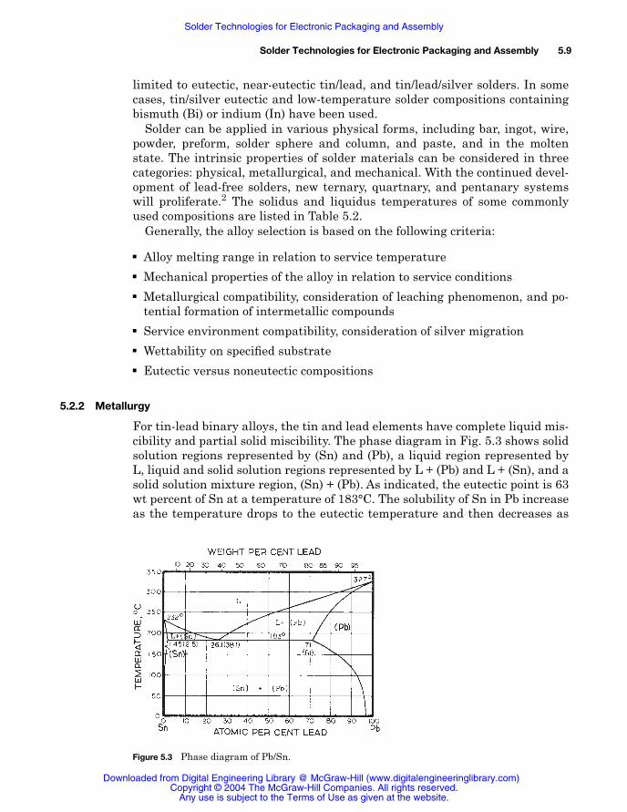
5.2.2 Metallurgy
For tin-lead binary alloys, the tin and lead elements have complete liquid mis-cibility and partial solid miscibility. The phase diagram in Fig. 5.3 shows solidsolution regions represented by (Sn) and (Pb), a liquid region represented byL, liquid and solid solution regions represented by L + (Pb) and L + (Sn), and asolid solution mixture region, (Sn) + (Pb). As indicated, the eutectic point is 63wt percent of Sn at a temperature of 183°C. The solubility of Sn in Pb increaseas the temperature drops to the eutectic temperature and then decreases as
Figure 5.3 Phase diagram of Pb/Sn.
Solder Technologies for Electronic Packaging and Assembly
Any use is subject to the Terms of Use as given at the website.
Solder Technologies for Electronic Packaging and Assembly 5.11
the temperature continues to drop. The same applies to the solubility of Pb inSn.
The maximum solubility of Pb is Sn is 2.5 wt percent; of Sn in Pb, it is 19 wtpercent. During soldering, the molten solder alloy wets the substrate with theaid of fluxes. Since the metallic surfaces involved in soldering tend to get oxi-dized or tarnished, the wettability depends to a large extent on the chemistryand reactions of fluxes. Nonetheless, the wetting phenomenon follows the ba-sic wetting principle. For a system at a constant temperature T and pressureP,
where G = free energyA = areaγ = surface tension
Then, the thermodynamic condition for spreading to occur is
The spreading of a liquid with negligible vapor pressure on a solid surface Sis as follows:
Thus,
where γls, γvl, and γsv are liquid-solid, liquid-vapor, and solid-vapor interfacialtension, respectively. Therefore, for spreading to occur,
or
In general, for a system with liquid to wet the solid substrate, spreading oc-curs only if the surface energy of the substrate to be wetted is higher than thatof the liquid to be spread.
∂G∂A-------
PT
γ=
∆G 0<
∂G∂A-------
–P ,T
γ sv γ ls γvl θcos+( )–=
γ sv γ ls γvl θcos+( ) 0>–
γ sv γ ls γvl θcos+>
Solder Technologies for Electronic Packaging and Assembly
Any use is subject to the Terms of Use as given at the website.
5.12 Chapter 5
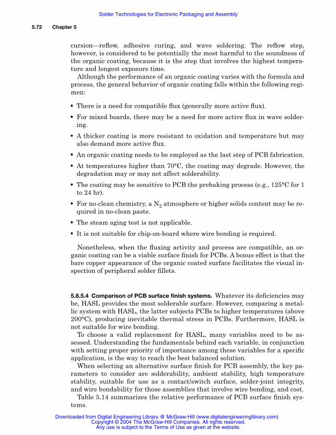
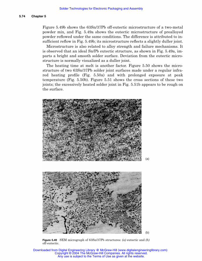
As the molten solder solidifies during cooling to form solder joints, the cool-ing process, including as the cooling rate, has a direct bearing on the resultingsolder joint as to its microstructure and the development of voids. Figure 5.4exhibits the SEM microstructure of 63 Sn/37 Pb melt under slow cooling, andFig. 5.5 exhibits the microstructure under fast cooling, with other conditionsbeing kept equal.
Because tin-lead solder alloys contain a solvus line and multiple solidphases, as shown in Fig. 5.3, they can be readily affected by heat treatment.
5.2.3 Solder powder2
Alloy powders can be produced by one of the common techniques—chemicalreduction, electrolytic deposition, mechanical processing of solid particulates,and atomization of liquid alloys.
Alloy powders made from chemical reduction under high temperature aregenerally spongy and porous. The fine particles of noble metal powders arefrequently precipitated by reduction of the salts in aqueous solution withproper pH. The precipitate slurry is then filtered, washed, and dried underhighly controlled conditions. A mechanical method is generally used to pro-duce flake-like particles. Metals possessing high malleability, such as gold(Au), silver (Ag), copper (Cu), and aluminum (Al), are most suitable for mak-ing flakes.
The electrolytic deposition process is characterized by dendrite particles,and it produces high-purity powders. The resulting particle sizes are affectedby the type, strength, and addition rate of the reducing agent and by other re-
Figure 5.4 SEM micrograph of 63Sn/37Pb under slow cooling.
Solder Technologies for Electronic Packaging and Assembly
Any use is subject to the Terms of Use as given at the website.
Solder Technologies for Electronic Packaging and Assembly 5.13
action conditions. The characteristics of the particles are also affected by cur-rent density, electrolytes, additives, and temperature. The principle ofatomization is used to disintegrate the molten metal under high pressurethrough an orifice into water or into a gaseous or vacuum chamber. The pow-ders produced by this method have relatively high apparent density, good flowrate, and are spherical in shape, as shown in Figs. 5.6 and 5.7. Powders to beused in solder paste are mostly produced by atomization because of its desir-able inherent morphology and the shape of the resulting particles. Hence, thediscussion that follows is concerned with the atomization technique only.
Figure 5.8 is a schematic of an inert gas atomization system with optionsof a bottom pouring system and a tilting crucible system. The system con-sists of a control cabinet, vacuum induction furnace, tundish, argon supplyline, ring nozzle, atomization tower, cyclone, and powder collection con-tainer. The alloy is melted under inert gas at atmospheric pressure to avoidthe evaporation of component ingredients. A high melt rate can be achieved.The molten material is then charged into the atomization tower. The melt isdisintegrated into powder at atmospheric pressure by an energy-rich streamof inert gas. The process conducted in a closed system is able to producehigh-quality powder.
In addition to inert gas and nitrogen atomization, centrifugal and rotatingelectrode processes have been studied extensively. The atomization mecha-nisms and the mean particle diameter are related to the operating parameters(diameter D, melting rate Q, and angular velocity ω of the rotating electrode)and to the material parameters (surface tension at melting point γ, dynamicviscosity η, and density at melting point ρ of the atomized liquid). The rela-tionships among these parameters are presented subsequently.
Figure 5.5 SEM micrograph of 63Sn/37Pb under fast cooling.
Solder Technologies for Electronic Packaging and Assembly
Any use is subject to the Terms of Use as given at the website.
Solder Technologies for Electronic Packaging and Assembly 5.15
It has been found that the mean volume-surface diameter d is proportionalto the surface tension of the atomized liquid and the melting rate but in-versely proportional to the angular velocity of the rotating electrode, the di-ameter of the electrode, and the density of the atomized liquid, expressed bythe following relation:
where the symbols were defined earlier.3–5
The mass proportion of secondary particles Ps is directly related to the an-gular velocity of the rotating electrode, the density of the atomized liquid, andthe melting rate but inversely proportional to the diameter of the electrodeand the surface tension of the atomized liquid, expressed by the following rela-tion:
Metal powder can also be produced by vacuum atomization, which is believedto yield clean and finer particles. For superfine alloy powder, it is reported thata new atomizing technique is available using pulverizing energy produced by a
Figure 5.8 Schematic of an inert gas atomization system.
Any use is subject to the Terms of Use as given at the website.
5.16 Chapter 5
50-MPa water pump concentrated at the apex of a conical jet by which the thinstream of molten metal is disintegrated into superfine droplets.6
Ultrasonic gas atomization is another technique that produces metal pow-ders successfully.7 A process of two-stage spinning cup atomization with a liq-uid quenching is in development to produce fine particles with greaterlatitude in particle-size control.8
5.2.4 Mechanical properties
Three fundamental mechanical properties of solders include stress vs. strainbehavior, creep resistance, and fatigue resistance.
Although stress can be applied by tension, compression, or shear force, mostalloys are weaker in shear than in tension or compression. Shear strength is im-portant, because most solder joints are subjected to shear stress during service.
Creep is a global plastic deformation that results when both temperatureand stress (load) are kept constant. This time-dependent deformation can oc-cur at any temperature above absolute zero. However, creep phenomena onlybecome significant at “active” temperatures.
Fatigue is the failure of alloys under alternating stresses. The stress that analloy can tolerate under cyclic loading is much less than that under staticloading. Therefore, the yield strength, a measure of the static stress that sol-ders will resist without permanent deformation, often does not correlate withfatigue resistance. The fatigue crack usually starts as several small cracksthat grow under repeated applications of stress, resulting in a reduction of theload-carrying cross section of the solder joint.
Solder in electronic packaging and assembly applications normally under-goes low cycle fatigue (a fatigue life less than 10,000 cycles) and is subjected tohigh stresses. Thermomechanical fatigue is another test mode used to charac-terize the behavior of solder. It subjects the material to cyclic temperature ex-tremes, i.e., a thermal fatigue test mode. Either method has its uniquefeatures and merit, yet both impose strain cycling on solders.
The ultimate tensile strength, 0.2 and 0.01 percent yield strength, and uni-form elongation of common bulk solder alloys are listed in Table 5.3. In thegroup of Sn/Pb alloys, the strength decreases with decreasing tin content. Thistrend is expected, with the exception that the eutectic composition does notshow the maximum strength. Its origin needs further confirmation.
The 96.5Sn/3.5Ag, 95Sn/5Ag, and 95Sn/5Sb compositions exhibit signifi-cantly higher strength and lower elongation. The composition 42Sn/58Bi isparticularly strong, yet extremely brittle. In/Sn alloys with high indium con-tent are extremely soft and lack adequate strength. It has been demonstratedthat the solder joint strength may not coincide with that of bulk solder alloysbecause of other external factors, such as solder joint configuration, metallur-gical reactions, interfacial wettability, interfacial effect, and the characteris-tics of other materials incorporated in the assembly.
Figures 5.9 through 5.30 show the creep behavior of solder alloys under aconstant load of 920 g (equivalent to 50 × 106 dyn/cm2 initial stress) at an am-bient temperature of 25 ± 3°C.
Solder Technologies for Electronic Packaging and Assembly
Any use is subject to the Terms of Use as given at the website.
Solder Technologies for Electronic Packaging and Assembly 5.17
Alloys of Sn/Ag, Sn/Sb, and 5Sn/85Pb/10Sb impart high creep resistance, asshown in Figs. 5.9 through 5.12. This is primarily attributed to solution hard-ening as substantiated by their high strength and low elongation. When loadis applied, the deformation is hindered by means of either interaction of soluteatoms with dislocations or interaction with the formation and movement ofvacancies, resulting in the impediment of the dislocation movement. Figure5.13 is a creep curve for the composition 85Sn/10Pb/5Sb, exhibiting relatively
TABLE 5.3 Tensile Strength and Uniform Elongation of Common Solders
Alloy composition Liquidus, °C Solidus, °C
Ultimatetensile strength,
103 lb/in2
0.2% yieldstrength,103 lb/in2
0.01% yieldstrength,103 lb/in2
Uniformelongation,%
42Sn/58Bi 138 138 9.71 6.03 3.73 1.3
43Sn/43Pb/14Bi 163 144 5.60 3.60 2.77 2.5
30In/70Sn 175 117 4.67 2.54 1.50 2.6
60In/40Sn 122 113 1.10 0.67 0.53 5.5
30In/70Pb 253 240 4.83 3.58 3.08 15.1
60In/40Pb 185 174 4.29 2.89 2.06 10.7
80Sn/20Pb 199 183 6.27 4.30 2.85 0.82
63Sn/37Pb 183 183 5.13 2.34 1.91 1.38
60Sn/40Pb 190 183 4.06 2.06 2.19 5.3
25Sn/75Pb 266 183 3.35 2.06 1.94 8.4
10Sn/90Pb 302 268 3.53 2.02 1.98 18.3
5Sn/95Pb 312 308 3.37 1.93 1.83 26.0
15Sn/82.5Pb/2.5Ag 280 275 3.85 2.40 1.94 12.8
10Sn/88Pb/2Ag 290 268 3.94 2.25 2.02 15.9
5Sn/93.5Pb/1.5Ag 301 296 6.75 3.85 2.40 1.09
1Sn/97.5Pb/1.5Ag 309 309 5.58 4.34 3.36 1.15
96.5Sn/3.5Ag 221 221 8.36 7.08 5.39 0.69
95Sn/5Ag 240 221 8.09 5.86 3.95 0.84
95Sn/5Sb 240 235 8.15 5.53 3.47 1.06
85Sn/10Pb/5Sb 230 188 6.45 3.63 2.62 1.40
5Sn/85Pb/10Sb 255 245 5.57 3.67 2.26 3.50
95Pb/5Sb 295 252 3.72 2.45 1.98 13.70
95Pb/5In 314 292 3.66 2.01 1.79 33.0
Solder Technologies for Electronic Packaging and Assembly
Any use is subject to the Terms of Use as given at the website.
Solder Technologies for Electronic Packaging and Assembly 5.25
lower creep resistance than 5Sn/85Pb/10Sb. Their melting point may be a fac-tor in creating such a difference.
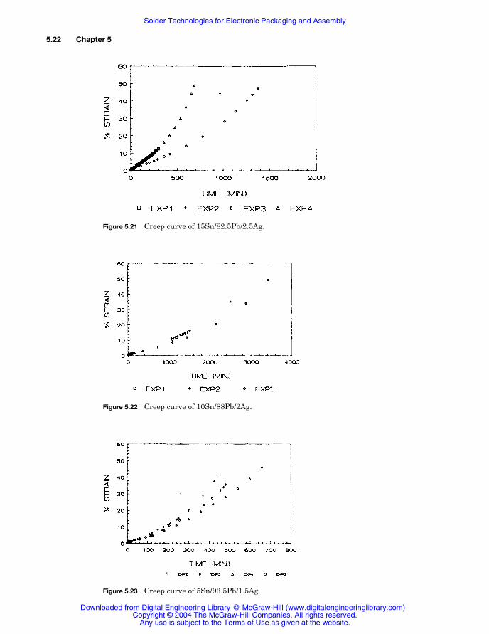
Figures 5.14 through 5.19 show the creep curves for Sn/Pb compositions.Eutectic 63Sn/37Pb has higher creep resistance than noneutectic composi-tions 60Sn/40Pb, 80Sn/20Pb, and 25Sn/75Pb. Alloys 10Sn/90Pb and 5Sn/95Pb,however, benefited from the high melting point of their microstructural con-tinuous phase, resulting in the more sluggish steady-state creep, as shown inFigs. 5.18 and 5.19. This is attributed to lower self-diffusion, although the al-loys are ductile and have moderate strengths. The creep curves for Sn/Pb/Agsystems are shown in Fig. 5.20 through 5.24. 62Sn/36Pb/2Ag has the highestcreep resistance. Its mechanism, whether through the impediment of grain-boundary sliding resulting from silver segregation or the result of high activa-tion energy for the dislocation movement, is not substantiated.
Bismuth alloys, 42Sn/58Bi and 43Sn/43Pb/14Bi, though having high tensilestrength, are found prone to creep. This may be primarily a result of their lowmelting temperatures and the predominance of the diffusion-controlled pro-cess. The corresponding creep curves are shown in Figs. 5.25 and 5.26. The In/Sn system has very poor creep resistance, as reflected in Figs. 5.27 and 5.28.The low melting point of their microstructural continuous phase is considereda main factor. While In/Pb compositions are ductile, as shown in the elonga-tion data, the single-phase microstructure and moderate melting points pro-vide moderate creep resistance, as shown in Figs. 5.29 and 5.30.
The creep resistance of the various solder alloys, as shown in Table 5.4, isranked in five groups—low, low-moderate, moderate, moderate-high, andhigh. As the testing temperature or the applied load changes, a change in thecreep behavior of the alloys may result.
5.3 Solder Paste
Solder paste, by its virtue of deformability and tackiness, is the primary mate-rial to make solder connections for surface mount and advanced surfacemount processes when it is applied on the mother board (main circuit board)
Figure 5.30 Creep curve of 60In/40Pb.
Solder Technologies for Electronic Packaging and Assembly
Any use is subject to the Terms of Use as given at the website.
5.26 Chapter 5
and/or when it is used for IC packaging on the module and package level. Thedeformable form of solder paste makes it applicable in any selected shape andsize and readily adaptable to automation; its tacky characteristics provide thecapability of holding parts in position without the need of additional adhesivesbefore the permanent bonds are formed.
5.3.1 Definition
Solder paste, by one definition, is a homogeneous and kinetically stable mix-ture of solder alloy powder, flux, and vehicle, which is capable of forming met-allurgical bonds at a set of soldering conditions and can be readily adapted toautomated production in making reliable and consistent solder joints.
In terms of functionality, a solder paste can be considered as being com-posed of three major components. These are solder alloy powder, vehicle sys-tem, and flux system. The vehicle primarily functions as a carrier for the alloypowder, a compatible matrix for the flux system, and a basis for a desirablerheology. The flux cleans the alloy powder and the substrates to be joined sothat high-reliability metallic continuity results and good wetting can beformed. Both vehicle and flux are fugitive or nonfunctional in nature aftercompletion of the soldering. They are nevertheless crucial to the formation ofreliable, permanent bonds. On a permanent basis, the alloy powder part is theonly functional component in forming a metallurgical bond.
5.3.2 Characteristics
The chemical and physical characteristics of solder paste can be representedby the following parameters:
TABLE 5.4 Relative Creep Resistance of Common Solder Alloys
Alloy composition Rank Alloy composition Rank
42Sn/58Bi Moderate 5Sn/95Pb Moderate–high
43Sn/43Pb/14Bi Low–moderate 62Sn/36Pb/2Ag High
30In/70Sn Low 15Sn/82.5Pb/2.5Ag Moderate
60In/40Sn Low 10Sn/88Pb2Ag Moderate–high
30In/70Pb Moderate 5Sn/93.5Pb/1.5Ag Moderate
60In/40Pb Moderate 1Sn/97.5Pb/1.5Ag Moderate
80Sn/20Pb Moderate 96.5Sn/3.5Ag High
63Sn/37Pb Moderate 95Sn/5Ag High
60Sn/40Pb Low 95Sn/5Sb High
25Sn/75Pb Low 85Sn/10Pb/5Sb Moderate
10Sn/90Sb Moderate 5Sn/85Pb/10Sb High
Solder Technologies for Electronic Packaging and Assembly
Any use is subject to the Terms of Use as given at the website.
Solder Technologies for Electronic Packaging and Assembly 5.27
Physical appearance Stability and shelf life Viscosity Cold slump Dispensability through fine needles Screen printability Stencil printability Tack time Adhesion Exposure life Quality and consistency Compatibility with surfaces to be joined Flow property before becoming molten Wettability Dewetting phenomenon Solder balling phenomenon Bridging phenomenon Wicking phenomenon Leaching phenomenon Quantity and properties of residue Residue corrosivity Residue cleanability Solder-joint appearance Solder-joint voids
5.3.3 Fluxes and fluxing9
The fundamental key to good solderability lies in ensuring that the surfaces tobe joined are “scientifically” clean. Cleanliness must then be maintained dur-ing soldering so that a metallic continuity at the interface can be achieved.This cleaning process is called fluxing, and the material used is the flux.
Customarily, the flux is classified based on its activity and chemical nature,namely rosin-based such as RMA, water-soluble, and no-clean.
Fluxes are applied to the surface to react with metal oxides or nonmetalliccompounds, thus “cleaning” them from the metal surfaces. Common metalsurfaces that are soldered include Sn/Pb, Sn, Cu, Au, Ag, Pd, Au/Pd, Ag/Pd,Au/Pt, Au/Ni, Pd/Ni, and Ni. Each has its own associated fluxing chemistry.
The flux activity can be determined by the combined measurements in waterextract resistivity, copper mirror test, halide test, and surface insulation test.
Solder Technologies for Electronic Packaging and Assembly
Any use is subject to the Terms of Use as given at the website.
5.28 Chapter 5
To achieve fluxing, several approaches are available. Flux can be incorpo-rated into the solder paste or inside the solder wire, it can be applied as a sep-arate chemical directly onto the component and solder paste or inside thesolder wire, or it can be applied as a separate chemical directly onto the com-ponent and solder pad surface, as with liquid flux used in wave soldering. Stillanother approach is gas-phase fluxing, which supplies a proper atmosphere tothe soldering substrates. Other in-situ cleaning process may render the solderfluxless.
5.3.4 Strength of fluxes
The fluxing strength depends on the intrinsic properties of the flux agent orflux system as well as the external conditions. The factors include the follow-ing:
Functional group and molecular structure of flux agent Melting point and boiling point of flux chemicals Thermal stability in relation to soldering conditions Chemical reactivity in relation to soldering conditions Surrounding medium of flux agent Substrates to be fluxed Environmental stability (temperature, humidity) Soldering conditions (temperature versus time, atmosphere)
The effects of molecular structure and medium on the strength of acids andbases are classified as inductive, resonance, hydrogen bonding, solvation, hy-bridization, and steric effects. For commonly adopted inductive effect, theelectronic-withdrawing groups adjacent to the carboxylic group of moleculesenhance the acidity strength of the carboxylic group as a result of anion stabi-lization. Conversely, electron-releasing groups decrease the acidity.
5.3.5 Water-cleaning flux
Water-cleaning flux is designed so that its residue after soldering can be re-moved by using either pure water or a water medium with the addition of asaponifier or an additive.
Considering performance, process, reliability, and cost, a flux chemistry thatrequires only water for removal (water-soluble) is the preferred choice. Specialnotes for using water-soluble solder paste are as follows:
In the cleaning process, to avoid flux entrapment and incomplete residue re-moval, ultrasonic cleaning is an effective aid.
In the soldering process, it is important to control the temperature profile,particularly in terms of peak temperature and dwell time at peak tempera-ture to avoid overheating.
Solder Technologies for Electronic Packaging and Assembly
Any use is subject to the Terms of Use as given at the website.
Solder Technologies for Electronic Packaging and Assembly 5.29
5.3.6 Gas-phase flux
Soldering under controlled-atmosphere conditions has been studied in recentyears. Such controlled atmospheres can generally be classified as either reac-tive or protective.
The reactive atmosphere can help the fluxing agent clean component leadsand solder pads. This approach has strong merits in solderability and leavesminimal residue. However, it should be cautioned that a reactive atmosphereis nonselective. It can react with all materials being exposed as long as theconditions meet thermodynamic and kinetic criteria. Therefore, all materialsof an assembly must be compatible with the reactive atmosphere. With thewide variety of materials used in each assembly and the continued incorpora-tion of new components and materials into assemblies, ensuring this compati-bility can be quite a task. The protective atmosphere, on the other hand,primarily functions as an oxygen and moisture repellent during solderingwithout providing external chemical activity. Controlled atmosphere solderingis discussed in Sec. 5.4.6.
5.3.7 No-clean flux
From the user’s point of view, no-clean flux (especially incorporated directlyinto solder paste) requires the following:
Minimal amount of residue; ideally none Residue that is translucent and aesthetically acceptable Residue that will not interfere with bed-of-nails testing Residue that will not interfere with conformal coating where applicable Residue that is nontacky Residue that stays inert under exposure to temperature, humidity, and volt-
age bias Ability to flux effectively without solder-ball formation
Because of the wide variety of design and performance requirements inboard assemblies, the acceptable amount of residue and the physical andchemical properties of the residue will vary from one application to another.An application-specific approach is needed. Success with a no-clean productrequires close communication and collaboration between user and supplier todesign a best-fit flux (material) and fluxing (process) system.
Common solder paste tests in chemical and physical characteristics con-tinue to apply to no-clean systems. The industry’s established test parametersand methods can be used to assess the quality and properties of the assem-blies. These include ionic contaminant test and visual examination. However,the tests for no-clean system have one difference. These tests should be con-ducted after reflow or soldering. The solder paste chemical makeup measure-ment in terms of ionic mobility must be also taken after exposure to aspecified reflow condition, not before exposure. This procedure is designed to
Solder Technologies for Electronic Packaging and Assembly
Any use is subject to the Terms of Use as given at the website.
5.30 Chapter 5
target the characteristics of the residue left on the board, not the as-is pastechemistry.
5.3.8 Comparison between water-clean and no-clean
With proper cleaning process and reflow parameters, a water-soluble processcan produce clean assemblies in both function and appearance. In addition,the nature of its chemistry imparts wider fluxing latitude, better accommodat-ing the inherent variations in solderability of components and boards. It re-quires initial equipment capital, added operating costs in energy and waterconsumption, and expenditures on consumables for a closed-loop recycle sys-tem.
No-clean (air) systems eliminate one process step, which is clearly an eco-nomic advantage. It should be noted that the cleaning process has been per-ceived as a step to remove residues from solder flux or paste, yet it actuallyhas provided the cleaning function for components and boards for many oper-ations without being noticed. It is not unusual for boards, before fluxing andsoldering, to contain higher amounts of ionic contaminants than after solder-ing and cleaning. The level of as-received contamination may exceed the ac-ceptable level, because most steps in board fabrication and component platinginvolve highly ionic chemicals.
For a no-clean system that requires soldering under a protective atmo-sphere such as N2, the cost of N2 may offset or exceed the savings gained fromno-clean operations, depending on N2 consumption and the unit cost of N2,which varies with the location. Other factors that may also complicate the as-sessment of a no-clean system are solder ball effect and the acceptability ofresidue appearance.
Nonetheless, both water-clean and no-clean routes are viable applicationsystems. A basic understanding of the principles behind each practice and thecompliance with application requirements is essential to the success of imple-menting either manufacturing system. Table 5.5 summarizes the general fea-ture comparison between water-clean and no-clean, and Table 5.6 illustratesviscosity and metal load of despensing and printing pastes.
TABLE 5.5 Comparison of Water-Soluble vs. No-Clean (Air)
Water-soluble No-clean (air)
Merits • Clean assembly in function and appearance• Latitude for solderability variation
• One less process step• Lower operating and capital expenses
Drawbacks • Extra step of process-cleaning• Operating cost—water, energy, and
consumables• Initial capital expenditure
• Unable to remove contaminants from board and components
• Often demand higher level of process control• Uncertainty in solder ball effect• Appearance issue• Possible limits for high-frequency application
and/or uses that demand extraordinary extension of fatigue
Solder Technologies for Electronic Packaging and Assembly
Any use is subject to the Terms of Use as given at the website.
Solder Technologies for Electronic Packaging and Assembly 5.31
5.3.9 Rheology
Paste applicability depends on its rheology, that is, its flow and deformationbehavior. The primary driving forces underlying the rheology of solder pasteinclude both kinetic and thermodynamic contributions. Therefore, the rheol-ogy of solder paste may be affected by the following factors:
Composition, shape, and size of suspended particles Chemical composition of suspending matrix Relative concentration of effective ingredients in matrix Structure of ingredients in matrix Interactions between matrix and suspended particles either physical or
chemical in nature, including wetting and solvation Volume fraction occupied by suspended particles—usually, the higher the
amount of particles, the more deviation from viscous flow Internal structure and its response to external forces Interactions among particles and resulting aggregates and flocculants Temperature
The difficulty of predicting the rheology of such a system is apparent and aresult a lack of knowledge of the detailed structure and the nature of forcesexerted by molecules or particles. However, its behavior can be characterized.It is also apparent that solder paste is not an elastic material, nor is it a pureviscous material. Viscoelasticity best describes the behavior of solder paste.The characterization of viscoelasticity and fundamental theories are coveredin the literature.1,10
The common methods used to transfer solder paste consistently and accu-rately onto the intended solder pads include mesh screen printing, metalmask stencil printing, pneumatic dot and line dispensing, and positive dis-placement dispensing. Figures 5.31 and 5.32 illustrate the flow behavior of adispensing paste and a printing paste, respectively.1 The paste possessing alow yield point and very slight plastic behavior is found most suitable for dis-pensing applications, and a moderate yield point and thixotropy are generallyassociated with the printing paste. Table 5.6 lists typical viscosity and metalload percentages for dispensing and printing application techniques.
TABLE 5.6 Viscosity and Metal Load of Dispensing and Printing Pastes
Any use is subject to the Terms of Use as given at the website.
5.32 Chapter 5
The size distribution of particles suitable for solder paste ranges from 45to 74 µm in diameter, corresponding to –200/+325 mesh, are compatible withthe printing standard of 0.050- to 0.25-in pitch land patterns, as well aswith dispensing up to 20 gauge. For finer-pitch applications, smaller than0.025-in pitch or 20 gauge, solder powder smaller than 45 µm in diameter isneeded.11
The printing thickness is another factor. Although the thicker paste depositmay impart a “better” joint, the maximum paste thickness for 0.050-, 0.025-,
Figure 5.31 Flow curve of dispensing paste.
Figure 5.32 Flow curve of printing paste.
Solder Technologies for Electronic Packaging and Assembly
Any use is subject to the Terms of Use as given at the website.
Solder Technologies for Electronic Packaging and Assembly 5.33
and 0.012-in pitch land patterns are generally limited to 0.015, 0.008, and0.004 in, respectively.
5.3.10 Formulation
As an example, a typical RMA solder-paste formula may contain 10 to 15 in-gredients that provide various intended functions as shown in Table 5.7. Theformula may appear to be straightforward. However, designing a viable prod-uct capable of delivering all the desired performance characteristics is com-plex and requires understanding the technologies.
The following thinking steps are one route to take in developing a product:
1. Define performance objective.
2. Utilize fundamental technologies.
3. Select raw materials.
4. Understand and anticipate potential synergistic or antagonistic interac-tions between ingredients.
5. Balance performance parameters.
6. Fine-tune the formula to meet designated specifications.
7. Develop production process.
8. Produce consistent product.
A product involves many performance parameters, and some of them aretrade-offs. For example, a high metal content is beneficial to solder joint vol-ume and reduced voids and residue, yet it makes the paste more prone to dry-ing and difficult to apply. A high-viscosity paste may improve flow controlagainst temperature, but it causes the paste to be difficult to apply. Using
TABLE 5.7 Ingredients of Typical RMA Solder Paste
Ingredient Function
Rosin Rosin system for designated softening point, acid number, thermal stability, fluxing activation, tackiness
Nonhalogen activator Activator system for accomplishing fluxing action over a wide range of temperatures, rheology
Solvent Solvent system to accommodate solubility, rheology, temperature compatibility, chemical compatibility
Any use is subject to the Terms of Use as given at the website.
5.34 Chapter 5
highly active fluxing chemicals may improve solderability in some cases, buttheir use may leave a more corrosive residue. In such cases, improving the sol-derability by selecting the proper ingredients without the use of highly activefluxing chemicals is the essence of technology. It should be noted that increas-ing the flux content does not always improve solderability in terms of wettingor the elimination of solder balling.
After the product has been designed, developing a reproducible process formaking the paste with consistent characteristics is equally important. It is notan exaggeration, but an indication of the importance of the role of the process,to state that the identical composition formula can produce different resultswhen the process is allowed to vary.
The design of water-soluble and no-clean products follows the same princi-ple, but specific chemical ingredients differ.
5.3.11 Design and use of solder paste for system reliability
With the versatility of components and the vast variation in their solderabil-ity, it is tempting to formulate a flux chemistry with high activity. It is alsoconvenient to incorporate the halide-containing organic ingredients to en-hance the activity without adversely affecting the test results in the content ofionic species. This is because organic halides can be very effective fluxingagents in a very low dosage, thus relieving the level of elaboration (skills) informulation technology. In addition, in various chemical makeups, low-dosagehalides may be able to pass the “standard” tests. It is a well established factthat, among the chemical families, mobile halides are the most reactive spe-cies toward metals that make up the circuitry. Thus, their use should be dis-couraged.
Finer powder obviously facilitates the fine-pitch deposition via printing ordispensing. Undesirably, the paste with finer powder results in higher de-mand in the content, as well as in the activity of flux, and is more often proneto solder balling during reflow. Finer powder is also associated with highercost.
Thus, it is always advantageous to use the coarsest powder that is allowableby a flux/vehicle system for achieving the printability and dispensability sothat the reduced cost and proper flux activity can be obtained.
As the large or heavy array packages are incorporated in the assembly, thedisparity of heat transfer is heightened. In those cases, increasing the temper-ature has indeed accommodated most reflow results. However, from a reliabil-ity standpoint, the approach may not be sound when considering the advent ofheat-sensitive components, more complex PCB design, and increasingly versa-tile components contained in an assembly.
Reflow profiles based on slower heating and cooler temperature will be morein sync with today’s complex assemblies, minimizing in-process heat-induceddamage as well as the level of residual stress, which may cause problems suchas PBGA package cracking, board warpage, and board delamination. Thesethree areas affect not only the production floor first-pass defect rate and yieldbut also the long-term performance of the assembly.
Solder Technologies for Electronic Packaging and Assembly
Any use is subject to the Terms of Use as given at the website.
Solder Technologies for Electronic Packaging and Assembly 5.35
The principles of design and use of solder paste—mild flux, coarse powder,and low-temperature reflow profile—work in tandem, toward achieving thehighest system reliability.
5.3.12 Quality assurance tests
Tests to assure the properties and performance of a solder paste can begrouped into five parts: paste, vehicle, powder, reflow, and post reflow. Table5.8 summarizes the tests in each of the five parts.1
5.4 Soldering Methodology
5.4.1 Types
The commercially available reflow methods include conduction, infrared, va-por phase, hot gas, convection, induction, resistance, and laser. Each of thesereflow methods has its unique features and merits in cost, performance, or op-erational convenience. For localized and fast heating, laser excels over othermethods, with hot air in second place. For uniformity of temperature, vaporphase ranks first. For versatility, volume, and economy, convection and infra-red are the choices. Conduction heating, however, is a convenience for low-vol-ume and hybrid assembly. For conductive components requiring fast heatingand high-temperature soldering, induction heating meets the requirement.Table 5.9 summarizes the strength and limitations of each method.
5.4.2 Reactions and interactions
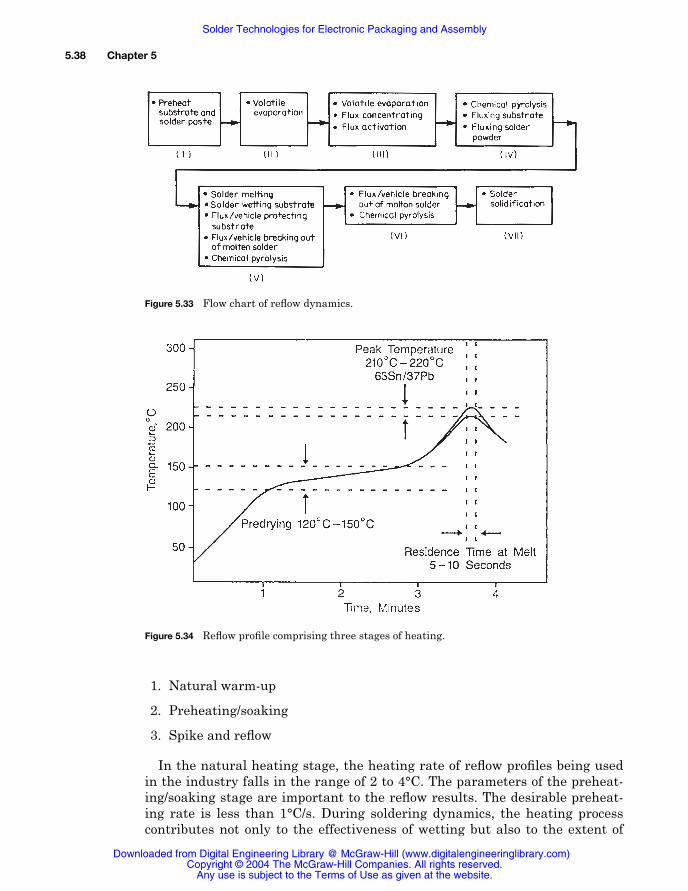
During soldering, a series of reactions and interactions occur in sequence or inparallel. These can be chemical or physical in nature in conjunction with heattransfer. The mechanism behind fluxing is often viewed as the reduction ofmetal oxides. Yet, in many situations, chemical erosion and dissolution of ox-ides and other foreign elements act as the primary fluxing mechanisms. Usinga more complex fluxing process in solder paste as an example, the primarysteps are represented by the flowchart in Fig. 5.33.
5.4.3 Process parameters
With the prevalence of infrared and convection reflow, a few more words aboutfurnace profile and furnace operating parameters are pertinent. It should bestressed that the reflow is a dynamic heating process in that the condition ofthe workpiece is constantly changing as it travels through the furnace in a rel-atively short reflow time. The momentary temperature that the workpiece ex-periences determines the reflow condition; therefore, the reflow results.
It is ultimately important to establish a correlation between the set temper-ature of a given furnace, the measured temperature of the workpiece at eachspecified belt speed, and the soldering performance. The resulting correlationbetween soldering performance and temperature setting or profile provides a“workable range” for the assembly.
Solder Technologies for Electronic Packaging and Assembly
Any use is subject to the Terms of Use as given at the website.
5.36 Chapter 5
Under mass reflow operation, both heating and cooling steps are importantto the end results. It is generally understood that the heating and coolingrates of reflow or soldering process essentially contribute to the compositionalfluctuation of the solder joint. This is particularly true when there are signifi-cant levels of metallurgical reactions occurring between the Sn/Pb solder andsubstrate metals. In the meantime, the cooling rate is expected to be responsi-ble for the evolution of the microstructure.
TABLE 5.8 Summary of Quality Assurance Tests for Solder Paste
PasteAppearanceMetal content and flux-vehicle percentageDensityViscosityViscosity versus shear rateCold slumpHot slumpMolten flowTack timeDryabilityDispensabilityPrintabilityShelf stabilityStorage, handling, and safety
Flux/vehicleWater extract resistivityCopper mirror corrosionChloride and bromideAcid NumberInfrared spectrum fingerprint and other spectroscopies
Post reflowCleanliness, resistivity of solvent extractSurface insulation resistance, before and after cleaningSolder joint appearanceSolder voidsJoint strengthPower cyclingTemperature cyclingVibration testSimulated agingThermal shock
Solder Technologies for Electronic Packaging and Assembly
Any use is subject to the Terms of Use as given at the website.
Solder Technologies for Electronic Packaging and Assembly 5.37
The key process parameters that affect the production yield as well as theintegrity of solder joints include the following:
Preheating temperature Preheating time Peak temperature Dwell time at peak temperature Cooling rate
It should be stressed that the reflow in a furnace (infrared or convection) isa dynamic heating process in that the conditions of the workpiece are con-stantly changing as it travels through the furnace in a relatively short reflowtime. The momentary temperature that the workpiece experiences determinesthe reflow conditions and therefore the reflow result.
Figure 5.34 illustrates a simulated reflow profile comprising three stages ofheating:
TABLE 5.9 Outline of Benefits and Limitations of Reflow Methods
Reflow method Benefits Limitations
Conduction Low equipment capital, rapid temperature changeover, visibility during reflow
Planar surface and single-side attachment requirement, limited surface area
Infrared High throughput, versatile temperature profiling and processing parameters, easier zone separation
Mass, geometry dependence
Vapor phase condensation
Uniform temperature, geometry indepen-dence, high throughput, consistent reflow profile
Difficult to change temperature, tempera-ture limitation, relatively high operating cost
Hot gas Low cost, fast heating rate, localized heat-ing
Temperature control, low throughput
Convection High throughput, versatility Slower heating, higher demand for flux activity
Induction Fast heating rate, high temperature capac-ity
Applicability to nonmagnetic metal parts only
Laser Localized heating with high intensity, short reflow time, superior solder joint, package crack prevention
High equipment capital, specialized paste requirement, limit in mass soldering
Focused infrared Localized heating, suitable for rework and repair
Sequential heating, limit in mass soldering
White beam Localized heating, suitable for rework and repair
Sequential heating, limit in mass soldering
Vertical reflow Floor space saving, maintenance of desired throughput
Often more costly
Solder Technologies for Electronic Packaging and Assembly
Any use is subject to the Terms of Use as given at the website.
5.38 Chapter 5
1. Natural warm-up
2. Preheating/soaking
3. Spike and reflow
In the natural heating stage, the heating rate of reflow profiles being usedin the industry falls in the range of 2 to 4°C. The parameters of the preheat-ing/soaking stage are important to the reflow results. The desirable preheat-ing rate is less than 1°C/s. During soldering dynamics, the heating processcontributes not only to the effectiveness of wetting but also to the extent of
Figure 5.33 Flow chart of reflow dynamics.
Figure 5.34 Reflow profile comprising three stages of heating.
Solder Technologies for Electronic Packaging and Assembly
Any use is subject to the Terms of Use as given at the website.
Solder Technologies for Electronic Packaging and Assembly 5.39
metallurgical reactions between solder and the substrates to which the solderinterfaces, particularly the peak temperature and the dwell time at the tem-perature above the liquidus of the solder.
Several events occur during this stage, as shown in steps (2) and (4) of theflow chart (Fig. 5.33). These include temperature set to fit the specific flux ac-tivation temperature of the chemical system of the paste and the time at heatto fit the constitutional makeup of the paste. Inadequate preheating oftencauses a spattering problem that manifests itself as discrete solder balls. Toohigh a temperature or too long a time at the elevated temperature can resultin insufficient fluxing and/or overdecomposition of organic, causing solderballing or hard-to-clean residue (if the no-clean route is adopted). The recom-mended general conditions for the second stage are 120 to 150°C for a dura-tion of 45 to 150 sec. The third stage is to spike quickly to the peak reflowtemperature at a rate of 1.0 to 4.0°C/s. The purpose of temperature spiking isto minimize the exposure time of the organic system to high temperature,thus avoiding charring or overheating. Another important characteristic is thedwell time at the peak temperature. The rule of thumb in setting the peaktemperature is 20 to 50°C above the liquidus or melting temperature; e.g., forthe eutectic Sn/Pb composition, the range of peak temperatures is 203 to233°C.
The wetting ability is directly related to the dwell time at the specific tem-perature in the proper temperature range and to the specific temperature be-ing set. Other conditions being equal, the longer the dwell time, the morewetting is expected—but only to a certain extent; the same trend applies athigher temperatures. However, as the peak temperature increases or thedwell time is prolonged, the extent of the formation of intermetallic com-pounds also increases. An excessive amount of intermetallics can be detrimen-tal to long-term solder-joint integrity. Peak temperature and dwell timeshould be set to reach a balance between good wetting and to expel any non-solder (organics) ingredients from the molten solder before it solidifies, thusminimizing void formation.
For a given system, the cooling rate is directly associated with the resultingmicrostructure, which in turn affects the mechanical behavior of solder joints.2
It was found that the microstructural variation and corresponding failuremechanisms of solder joints that were made under various reflow temperatureprofiles are extremely complex. Nonetheless, some correlation between thecooling rate and the basic properties can be obtained.
The copper/solder/copper system is a good example, because it is still themost common material combination electronics assemblies. In this system, 63Sn/37Pb solder joins copper pads (coated or uncoated) on the printed circuitboard with the Sn/Pb coated copper leads of IC components.
For the tinned Cu-63Sn/37Pb-tinned Cu assembly, the reflowed solder jointsare cooled in five different manners that deliver four cooling rates—0.1°C/sec,1.0°C/sec, 50°C/sec, and 230°C/sec, respectively, as measured above 100°C.The fifth cooling mode was conducted in a two-step cooling, resulting an un-even cooling with an average cooling rate of 12°C/sec. Each of the five coolingmodes produced a different development of microstructure of solder joint.2
Solder Technologies for Electronic Packaging and Assembly
Any use is subject to the Terms of Use as given at the website.
5.40 Chapter 5
5.4.4 Reflow temperature profile
The reflow temperature profile, representing the relationship of temperatureand time during the reflow process, depends not only on the parameter set-tings but also on the capability and flexibility of equipment. Specifically, theinstantaneous temperature conditions that a workpiece experiences are deter-mined by
Temperature settings to all zone controllers Ambient temperature Mass per board Total mass in the heating chamber (load) Efficiency of heat supply and heat transfer
For furnace-type reflow process, two profiles are taken to illustrate the ef-fect of temperature profile on the reflow results.
Figures 5.35 and 5.36 show the actual temperature profiles of a convectionoven, first with a relatively lower preheat temperature, as shown in Fig. 5.35,and then a higher preheat temperature, as shown in Fig. 5.36. The impor-tance of the compatibility of solder paste chemistry and the assembly systemwith the reflow temperature profile can be easily demonstrated. For instance,if the solder paste and the assembly require the temperature profile of Fig.5.35, performing reflow under the temperature profile of Fig. 5.36 may giverise to the following phenomena:
Deficiency of flux, resulting in solder balls Overheating of organics, resulting in cleaning difficulty for processes that
are designed to include a cleaning step
On the other hand, if the paste is designed for the higher preheat tempera-ture and/or assembly requires additional heat, using the lower preheat tem-perature profile can produce the following phenomena:
Figure 5.35 Convection reflow profile with lower-temperature preheating.
Solder Technologies for Electronic Packaging and Assembly
Any use is subject to the Terms of Use as given at the website.
Solder Technologies for Electronic Packaging and Assembly 5.41
Uneven soldering, resulting in cold solder joints An excessive amount of residue remaining or non-dry residue from no-clean
paste
The temperature profile with boosted preheating conditions, as shown inFig. 5.36 is most useful for the assembly that is densely populated with com-ponents with a large disparity in mass.
Depending on the type of conveyorized furnace, the mass of the assemblyand the degree of loading, the major operating parameters to be monitoredfor effective reflow are the belt speed and the temperature settings of individ-ual zones. The relationship between temperature settings and belt speed; in-creasing belt speed decreases the resulting peak temperature while otherconditions are equal, as shown in Fig. 5.37. Because the required peak tem-perature is set at 20 to 50°C above the melting temperature of a solder alloy,the working range of peak temperature is always fixed. For every tempera-ture profile, a relationship between peak temperature and belt speed can be
Figure 5.36 Convection reflow profile with higher-temperature preheating.
Figure 5.37 Reflow oven beltspeed vs. peak temperature.
Solder Technologies for Electronic Packaging and Assembly
Any use is subject to the Terms of Use as given at the website.
5.42 Chapter 5
established, and usable range of belt speeds as depicted in Fig. 5.37 can beobtained.
5.4.5 Effects of reflow profile
The reflow profile used for surface mount manufacturing has a direct bearingon manufacturing yield, solder-joint integrity, and the reliability of the assem-bly. Specific areas that are affected by reflow profile are listed below. Eacharea may be affected, to a different degree, by one or more of the three heatingstages.
Temperature distribution across the assembly Plastic IC package cracking Solder balling Solder beading Wetting ability Residue cleanability Residue appearance and characteristics Solder joint voids Metallurgical reaction between solder and substrate surface Microstructure of solder joints Board warpage Residual stress level of the assembly
5.4.5.1 Uniformity of temperature distribution. In a normal reflow environment,temperature differential across the assembly is inevitable. This results fromthe large disparity in mass and in the characteristics of the components cou-pled with the relatively short total reflow time (the entire cycle lasts only sev-eral minutes). A large temperature differential causes uneven soldering,resulting in localized cold joints or overheated joints. These problematic jointsmay contribute to manufacturing defects or jeopardize the long-term integrityof the solder joints under service conditions if they are not detected as manu-facturing defects and corrected.
For a given oven, the rate of natural warm-up (in °C/sec) and the intendedpreheat temperature and time are the main factors that control temperatureuniformity across the assembly. A slower heating rate in the warm-up state isdesired to reach a more uniform board temperature distribution.
5.4.5.2 Plastic IC package cracking. Along with factors such as die size, themoisture sensitivity of the molding compound, and its thickness, reflow profileplays an important role in causing or preventing plastic IC package cracks.When the IC package (e.g., BGA, QFP, SOIC) absorbs a certain level of mois-
Solder Technologies for Electronic Packaging and Assembly
Any use is subject to the Terms of Use as given at the website.
Solder Technologies for Electronic Packaging and Assembly 5.43
ture during storage, handling, or transit (without proper dry pack), the ab-sorbed moisture may cause package cracking during reflow. Setting a properreflow profile can mitigate the cracking problem; the heating rate from ambi-ent temperature to 140 to 150°C is most critical.2
5.4.5.3 Solder balling. Elevated temperatures and excessive time at those tem-peratures during the warm-up and preheating stages can result in inadequatefluxing activity or insufficient protection of solder spheres in the paste, caus-ing solder balling. In addition to the quality of solder paste, the presence ofsolder balls may be essentially related to the compatibility between the pasteand the reflow profile. On the other hand, inadequate preheating or heatingtoo fast may cause spattering, as evidenced by random solder balls. The twoheating stages preceding the spike/reflow zone are primarily responsible forthis phenomenon.
5.4.5.4 Solder beading. Solder beading refers to the occurrence of large solderballs (usually larger than 0.005 in [0.13 mm] in diameter) that are always as-sociated with small and low-clearance passive components (capacitors and re-sistors). This problem will occur even when the paste may otherwise performperfectly, i.e., free of solder balls at all other locations (components) on theboard and with good wetting. The trouble with solder beading is that it mayoccur in most or all board assemblies, rendering the first-time yield to nearlyzero. The current remedy on the production floor is to manually remove thebeads.
The formation of solder beads near or under capacitors and resistors islargely attributed to paste flow into the underside of the component body be-tween two terminations aided by capillary effect. As this portion of paste meltsduring reflow, it becomes isolated away from the main solder on the wettablesolder pads, forming large discrete solder beads. With other factors, reflowprofile is a contributor to this phenomenon The practice of adopting a slowerpreheating rate and a lower reflow peak temperature can reduce solder bead-ing. However, if the reflow profile is at its optimum, and the problem still per-sists, a new paste with a strengthened chemistry is the solution.
5.4.5.5 Wettability. The temperature setting and time spent in both preheatingand spike/reflow affect wettability. However, each stage works by a separatemechanism. In the preheating stage, the range of temperature and the timespent in this range directly affect the activity of flux. Wettability, in turn, is af-fected by the fluxing action. However, in the spike/reflow zone, wetting on the“cleaned” surface is influenced by the peak temperature because of the intrin-sic wetting ability of molten solder alloy. This ability increases on a wettablesubstrate with higher temperature. With all other conditions being equal, alonger dwell time can, to a limited degree, further enhance wetting. Modifica-tion of the spike/reflow zone may sometimes solve a minor wetting problem.
Solder Technologies for Electronic Packaging and Assembly
Any use is subject to the Terms of Use as given at the website.
5.44 Chapter 5
5.4.5.6 Cleanability. In the case of solder paste that is designed to be cleaned,particularly water cleaned, excessive heat may make it difficult for the resi-due to be removed, rendering a normal cleaning process ineffective. In thiscase, all stages of the reflow profile can be contributors.
5.4.5.7 Residue appearance and characteristics. The importance of the compati-bility of the solder paste’s chemical composition with the reflow profile can bereadily demonstrated when using a no-clean soldering process. For instance, ifthe paste is reflowed with a temperature profile below the heat requirement, ahigher amount of residue than expected will remain. In addition, the charac-teristics of that residue may range from being tacky to ionically active.
5.4.5.8 Solder joint voids. Incomplete outgassing (gases entrapped in the sol-der joint) is the main cause of voiding. In addition to design factors, the com-patibility between the reflow profile and the chemical makeup of solder pasteis important. There should also be sufficient dwell time in the molten state(above 183°C for 63Sn/37Pb) to ensure that the gases have enough time toseparate and escape from the molten solder.
5.4.6 Optimal profile
The heat transfer from the surrounding hot air to the various components onthe board, such as leaded packages, array packages, and discretes, differs dur-ing the process such that a thermal equilibrium hardly exists. This disparitycan be compensated for by either setting a reflow profile with a higher heatsupply rate and higher temperature or one with a slower heating rate andlower temperature. On most manufacturing lines, unfortunately, a reflow pro-file with a higher heating rate and higher temperature is often used.
This disparity in the heat transfer may be heightened as large or heavy ar-ray packages are incorporated. Although increasing the temperature has ac-commodated most reflow results, the approach will not work well with heat-sensitive elements or with PCBs that contain increasingly versatile compo-nents.
The initial warm-up state plays a far more influential role in the qualityand reliability of assembled boards than was first thought. An initial heatingrate at less than 1°C/sec in conjunction with the heating rate for the rest ofprofile at not more than 3°C/sec is considered most beneficial and is recom-mended. Under SMT environments, the small degree of reduction in heatingrate would not be a bottleneck for production throughput. By using the slowerrate in the warm-up and preheating stages prior to reaching 183°C, the peaktemperature can be maintained in the range of 210 to 215°C, in contrast to215 to 230°C. The total dwell time above the liquidus temperature (183°C)falls in the range of 30 to 65 sec.
Reflow profiles bases on slower heating rates and cooler temperatures willbe more in line with today’s complex assemblies, minimizing in-process heatexposure as well as residual stress.
Solder Technologies for Electronic Packaging and Assembly
Any use is subject to the Terms of Use as given at the website.
Solder Technologies for Electronic Packaging and Assembly 5.45
5.4.7 Laser soldering1
Two types of laser have been applied to solder reflow—carbon dioxide (CO2)and neodymium-doped yttrium-aluminum-garnet (Nd:YAG). Both generateradiation in the infrared region with wavelengths of about 10.6 µm from theCO2 laser and 1.06 µm for the YAG laser. The wavelength of 1.06 µm is moreeffectively absorbed by metal than by ceramics and plastics; the wavelength of10.6 µm is normally reflected by conductive surfaces (metals) and absorbed byorganics.
The main attributes of laser soldering are short-duration heating and high-intensity radiation, which can be focused onto a spot as small as 0.002 in(0.050 mm) in diameter. With these inherent attributes, laser reflow is ex-pected to
Provide highly localized heat to prevent damage to heat-sensitive compo-nents and to prevent cracking of plastic IC packages
Provide highly localized heat to serve as the second or third reflow tool forassemblies demanding multiple-step reflow
Require short reflow time Minimize intermetallic compound formation Minimize leaching problems Generate fine-grain structure of solder Reduce stress buildup in solder joint Minimize undesirable voids in solder joint
With these attributes in mind, laser soldering is particularly beneficial tosoldering densely packed regions, where local solder joints can be made with-out affecting the adjacent parts, to soldering surface-mount devices onprinted-circuit boards having heat sinks or heat pipes, and to soldering multi-layer boards. In addition, it also provides sequential flexibility of solderingdifferent components and enhances the high-temperature performance of ad-hesives used for mounting surface-mount devices.
With respect to reflow time, laser soldering can be accomplished in less than1 sec, normally in the range of 10 to 800 ms. The laser can be applied to point-to-point connections through pulsation as well as to line-to-line connectionsvia continuous laser beam scan.
The fine-pitch flat-pack devices have been connected to printed wiringboards using YAG continuous laser beam scans on each side of the package.Both the use of prebumped solder pads and the direct application of solderpaste are feasible. In directly reflowing solder paste, although using spatter-ing and heat absorption problems have been observed, they are not incurable.To eliminate these problems, the preheating and predrying step is necessary.Location of laser beam impringement is another factor. In addition, compati-ble properties of solder paste have be designed to accommodate fast heating inrelation to fluxing and paste consistency, coupled with the proper design of theequipment and its settings.
Solder Technologies for Electronic Packaging and Assembly
Any use is subject to the Terms of Use as given at the website.
5.46 Chapter 5
In using the laser, another concern is energy absorption by the printed-cir-cuit boards, which leads to board damage. This is considered to have been cor-rected by switching from CO2 laser to YAG laser. Due to the wavelengthdifference, the energy absorption by polymers can be minimized. Lish11 hasfound that sometimes complications may occur. In assembling multilayerpolyimide boards by using laser as a second-step reflow, burning was found inthe board while it was moving under the laser. The burning was traced to thecolor pigments contained in the adhesive, which was used for attaching heatsinks. The problem was eliminated by using colorless pigment in the adhesive.This is another clear demonstration that a consideration of all materials inthe reflow process is needed.
Regarding the resulting solder joint, a fine-grain microstructure and the for-mation of significantly reduced intermetallic compounds at the copper and sol-der (63Sn/37Pb) interface have been observed when laser soldering was usedas compared to other reflow methods.12 Stress buildup in the solder joint dueto the difference in thermal expansion coefficients between the materials onboth sides of the solder joint is expected when the reflow method requires thewhole assembly to be exposed to the soldering temperature. Localized heatingand exposure of short duration by using a laser are expected to generate lessstress in the joint for the assemblies having materials of different thermal ex-pansion coefficients.
5.4.8 Controlled-atmosphere soldering13
5.4.8.1 Principle. Based on its function, the atmosphere may be considered aseither protective or reactive. A protective atmosphere normally is inert towarda specific soldering material under specific conditions, and a reactive atmo-sphere may involve either an oxidizing or a reducing function toward the sub-ject system.
Broadly, chemicals that can provide oxidizing or reducing potential in rela-tion to the specific metal-oxide system, and that can generate significant va-por pressure at an operating temperature, are expected to contribute to thefunctional nature of the total atmosphere.
Following is a list of some commonly used atmospheres. Their correspond-ing nominal compositions are summarized in Table 5.10.
Dry air Nitrogen Hydrogen Nitrogen-hydrogen blends at different ratios Dissociated ammonia Exothermic gas Nitrogen dopants at different concentrations
Solder Technologies for Electronic Packaging and Assembly
Any use is subject to the Terms of Use as given at the website.
Solder Technologies for Electronic Packaging and Assembly 5.47
The thermal cracking of methanol essentially yields hydrogen and carbonmonoxide at high temperatures, as represented by the chemical equation,
CH3OH = 2H2 + CO
At low temperatures (below 800°C), side reactions may occur, leading to theformation of H2, CH4, CO2, and C.
Each component of the atmosphere gases may function as oxidant or as re-ducing agent, depending on the temperature and its oxidation-reduction po-tential relative to that of the materials involved. Among the components ofcommon atmosphere gases, oxygen, water vapor, and carbon dioxide normallyserve as oxidants to most metals and metal oxides, and hydrogen and carbonmonoxide serve as reducing agents. The ratio of oxidant content to reducing-agent content, in relation to that ratio at equilibrium, indicates whether theresulting atmosphere is oxidizing or reducing.
During soldering, the reactions and interactions of chemicals in the solderpaste and between chemicals and the metal surface can be quite complex. Insimple terms, the mechanisms may include evaporation, pyrolysis, oxidation,and reduction. The generalized oxidation and reduction reaction can be ex-pressed as follows:
To obtain the thermodynamic equilibrium constant K for each of the preced-ing reactions,
xM(s) + yO2(g) ⇒ MxO2(s) (5.1)
(5.2)
TABLE 5.10 Percentage Composition of Atmosphere Gases
Any use is subject to the Terms of Use as given at the website.
5.48 Chapter 5
xM(s) + yCO2(g) ⇒ MxOy(s) + yCO(g) (5.3)
Assuming that the compositions of solids remain constant and the gases be-have ideally,
where a represents the activities of the individual reactants as well as theproducts of reactions (5.1), (5.2), and (5.3), and , , , and rep-resent the partial pressure of H2O, H2, CO, and CO2, respectively.
By introducing the relationship between the free energy ∆Go and the equi-librium constant,
it is shown that reactions (5.1), (5.2), and (5.3) can proceed in the forward orreverse direction, depending on the temperature and the ratios of , ,
, and .Figure 5.38 shows the standard free energy of formation for some metal-
metal oxide systems and CO/CO2, H2O/H2, and CO2/C atmospheres as a func-tion of temperature. Assuming that they are under equilibrium condition andat a soldering temperature of 250°C, lead oxide and copper oxide can be re-duced by hydrogen. However, hydrogen is not effective for tin oxides until thetemperature reaches 600°C. Equation (5.2) also indicates that the presence oftoo much water vapor in the furnace atmosphere will cause oxidation to cer-tain metals. The partial pressure of water vapor should therefore be main-tained at a constant and defined value.
At a given atmosphere, composition, and dew point, the gas flow rate andthe flow pattern of the exhaust systems in the furnace are also important fac-tors in soldering performance. The gas flow rate should be high enough toavoid localized atmosphere buildup as a result of local reactions. To achievethe best performance and cost results, the required flow rate is determined bythe characteristics of the solder paste being used, the furnace belt speed, load-ing pattern, belt width, and other furnace parameters. The exhaust efficiency
K2
ax
Ma
y
H2O
aMxOya
y
H2
--------------------------=
K3
aMxO2yaCO
y
aMx aCO2
y----------------------------=
K2
HP
2Oy
HP y
2
-----------------=K11
PO2
y---------= K3
COyP
CO2yP
--------------=
PH2O PH2PCO PCO2
∆G° RT Kln–=
PH2O PH2
PCO PCO2
Solder Technologies for Electronic Packaging and Assembly
Any use is subject to the Terms of Use as given at the website.
Solder Technologies for Electronic Packaging and Assembly 5.49
and its flow pattern, in combination with the flow rate, dominate the removalof volatile components generated from the pyroloysis and evaporation ofchemicals in solder material, which in turn affects solderability.
It should be noted that a complete burn-out process is normally not feasibleat the eutectic tin-lead or tin-lead-silver soldering temperature when using asolder paste. To obtain good solderability and quality solder joints, a metalliccontinuity at the interfaces between solder and substrate must be formed dur-ing soldering. When using a solder paste, a complete coalescence of solder-powder particles has to occur in synchronization with the development of me-tallic continuity at the interfaces. At the soldering temperature, the atmo-sphere surrounding the workpiece protects or interacts with the surface ofsubstrates, the solder alloys, and the chemical ingredients in the flux-vehiclesystem. These interactions determine the chemical and physical phenomenain terms of volatilization, thermal decomposition, and surface-interfacial ten-sion. A controlled atmosphere is expected to deliver a more consistent solder-ing process.
In addition to consistency, the inert or reactive atmospheres possess furthermerits. These include
Any use is subject to the Terms of Use as given at the website.
5.50 Chapter 5
Irregular residue charring prevention Polymer-based board discoloration prevention Wider process window Overall quality and yield improvement
The inert and reactive atmospheres are expected to facilitate conventionalfluxing efficiency during soldering. It should be noted, however, that perfor-mance results rely greatly on the specific atmospheric composition and itscompatibility with the solder material, substrate, and chemicals incorporatedin the system, which must also be compatible with the soldering temperatureprofile. Figure 5.39 shows that the solderability under N2 atmosphere is sig-nificantly improved, as solder balls that are formed under ambient air condi-tions are eliminated.
5.4.9 Process parameters15–18
5.4.9.1 Gas flow rate. The gas flow rate required to achieve a specific level ofoxygen in the dynamic state of the reflow oven is largely controlled by the type
Figure 5.39 Solderability performance of solder paste under N2 atmosphere vs. ambi-ent air, reflowed under (a) N2, (b) 95N2/5H2, (c) 85N2/15H2, (d) 70N2/30H2, (e) H2, and(f) ambient air.
Solder Technologies for Electronic Packaging and Assembly
Any use is subject to the Terms of Use as given at the website.
Solder Technologies for Electronic Packaging and Assembly 5.51
of oven, categorized as closed-system, semi-closed system, or open system. Therelationship of the flow rate versus oxygen level within one type of oven andthe relationship among the different types of oven are summarized in Fig.5.40. For a given oven, the required flow rate increases when the allowable ox-ygen level is lowered. At a given flow rate, when the air tightness in oven con-struction is reduced, the achievable oxygen level will be higher.
As expected, for a given reflow system, the oxygen level is inversely relatedto gas flow rate as shown in Fig. 5.41. The gas flow rate also affects the tem-perature distribution and temperature uniformity of assembly. Figure 5.42 ex-hibits the temperature gradient between the component PLCC-84 and theboard surface, indicating that a higher gas flow rate reduces the temperaturegradient of an assembly.14 However, the downside of using high flow rate goesto the higher gas consumption, therefore increasing cost. The cost impact maybe mitigated when the design of oven is capable of internal gas recirculation inan efficient fashion.
5.4.9.2 Humidity and water vapor pressure. Water vapor pressure inside the sol-dering govern can be contributed from the following:
Figure 5.40 Oxygen level of three types of reflowoven.
Figure 5.41 N2 flow rate vs. oxygen level.
Solder Technologies for Electronic Packaging and Assembly
Any use is subject to the Terms of Use as given at the website.
5.52 Chapter 5
The composition and purity of atmosphere The reaction product of flux/vehicle chemical system with metal substrates The moisture release from the assembly including components and board The ambient humidity
Because water vapor is essentially oxidizing to metal substrates that are tobe joined by soldering, its partial pressure in the oven affects the overall func-tion of the atmosphere.
The partial pressure of water vapor in an atmosphere gas is convenientlyexpressed as dew point—that is, the temperature at which condensation ofwater vapor in air takes place. The dew point can be measured by a hygrome-ter or dewpointer by means of fog chamber, chilled mirror aluminum oxidetechnique. The relationship of dew point with the vapor pressure is shown inFigs. 5.43 and 5.44. The relative humidity, RH, is related to the actual vaporpressure of water (or represented by dew point), Pw, and the saturated vaporpressure at the prevailing ambient temperature, Ps, as follows:
The purity of incoming gas in terms of moisture is normally monitored bymeasuring the dew point.
Figure 5.42 Temperature gradient vs. flow rate.
Figure 5.43 Dew point vs. vaporpressure (high).
RH PwPs-------=
Solder Technologies for Electronic Packaging and Assembly
Any use is subject to the Terms of Use as given at the website.
Solder Technologies for Electronic Packaging and Assembly 5.53
5.4.9.3 Belt speed. For an evenly spaced loading on the belt, the belt speed notonly determines the throughput, it also affects other operating parametersthat can alter the soldering results. As examples, the parameters that are af-fected by the change of belt speed include
Peak temperature—at fixed temperature settings, increasing the belt speedresults in the decrease of peak temperature.
Atmosphere composition—while other conditions are equal, the change ofbelt speed may alter the oxygen level (including moisture content).
5.4.9.4 Temperature. The operating temperature or temperature profile is anintegral part of soldering process. It affects the physical activity and chemicalreaction of the organic system in solder paste or flux. The operating tempera-ture, particularly peak temperature, changes the wetting ability of molten sol-der on the metal substrate; wetting ability generally increases with increasingtemperature. Chemical reactions and thermal decompositions respond to therising temperature and the temperature profile.
5.4.9.5 Oxygen level. Various studies have focused on the application of no-clean processes and on the determination of the maximum allowable oxygenlevel for using nitrogen-based no-clean soldering process in solder paste reflowand wave soldering.
Each study was performed with a specific solder paste and flux or with a se-lected series of paste and flux. Tests were conducted with specific equipmentunder a designated process. In view of the continued introduction of newequipment and the diversity of processes coupled with the versatility of solderpaste and flux compositions, the test results are expected to represent the spe-cific system (paste, oven, process, assembly) and at best to provide a guidelinereference point. For example, a solder paste from the Vendor I to be used withProcess A may require a maximum 20-ppm oxygen level to obtain good solder-ability, freedom from gross solder-ball effects, and acceptable after-solderingresidue. To achieve similar results, the same paste to be used with Process B
Figure 5.44 Dew point vs. vapor pressure (low).
Solder Technologies for Electronic Packaging and Assembly
Any use is subject to the Terms of Use as given at the website.
5.54 Chapter 5
may need a maximum of 300 ppm oxygen. The same could be true for a differ-ent paste used in the same process.
The precise oxygen level requirement for a no-clean soldering is impracticalto pin down. Instead, the general principle and trends in the relationship be-tween the performance feature and the allowable maximum oxygen level canbe derived. Figure 5.45 presents the trend of performance feature merit in re-lation to oxygen level for a series of solder paste containing various levels ofsolid contents. For a given performance feature, Fig. 5.46 shows the trend ofthe effect of solid content in no-clean paste on oxygen level requirement dur-ing reflow soldering. The performance feature denotes the solderability or thereduction in solder balling.
For convenience, solderability may be monitored by measuring wettingtime, wetting force, meniscus rise, or wetting angle, or by visual wetting qual-ity. The series of the curves represents the generic groupings of no-clean sol-der paste or flux by the level of solid contents. This is, however, based on thefact that the solid content possesses a good flux system. As shown in Fig. 5.45,
Figure 5.45 Dew point vs. vapor pressure (high).
Figure 5.46 Solid content in paste vs. performance fea-ture.
Solder Technologies for Electronic Packaging and Assembly
Any use is subject to the Terms of Use as given at the website.
Solder Technologies for Electronic Packaging and Assembly 5.55
the performance trend in the increasing solderability and decreasing solderballing is enhanced when the solid content increases, and, at a given solid con-tent beyond a threshold of oxygen level, the performance will significantlydrop. It should be noted that increasing solid content creates an increasingamount of after-soldering residue. The required oxygen level may fall in anyplace within the region, depending on other factors as discussed above. For agiven level of performance, the allowable oxygen level will be relieved as thesolid content increases, as depicted in Fig. 5.46.
5.4.9.6 Optimal O2 level. In general, with levels higher than 2,000 ppm O2, theeffect of nitrogen may hardly be detected. Below 20 ppm O2, the process willbecome difficult to control and, needless to say, too costly. For a given oven andprocess, the required O2 level is essentially controlled by the chemistry andmakeup of the solder paste. For example, a solder paste from Supplier A mayrequire a maximum level of 800 ppm O2 to obtain the desirable results (goodwetting, no solder balls, etc.). To achieve similar results, solder paste fromSupplier B may need a maximum of 200 ppm O2. In practice, O2 levels in therange of 20 to 2,000 ppm should be able to accommodate most applications.
Soldering under nitrogen poses two additional demands: more stringentprocess control and higher operating cost. However, its potential effects on sol-derability, heat transfer, PCB materials, and process window may bring bene-fits in mounting large-area and heavy BGAs as well as in connecting smalland delicate CSPs onto complex PCBs.
5.4.10 Profile temperature measurement
At a steady state, and when properly used, the thermocouple can readily mea-sure true temperature. However, in a dynamic environment, such as the re-flow process, the response efficiency of a thermocouple may affect the accuracyof the temperature measurement.
To accurately measure the temperature on a solid surface (or a point), thethermocouple must be in a direct and firm contact with the surface to be mea-sured. It is common to use attaching materials such as a high-temperaturesolder and high-temperature adhesive or Kapton® tape. The application of anyof these materials inevitably introduces an additional mass into the contactarea, which works as a thermal sink. The additional mass may skew tempera-ture readings, resulting in an understanding readout. For cases in which thetip of the thermocouple is broken away from the surface contact, the oven airtemperature, rather than the intended surface temperature, may be recorded.Thus, the amount of solder or adhesive used should be as small as possible,minimizing the barrier in heat transfer and thermal mass.
A more desirable technique, however, is to make contact without the use ofextraneous material. One system (by Saunders Technology) has demonstratedits usefulness and performance. Its design features include a unique thermo-couple probe mounted in a sliding ball joint and a detachable clamp. Theprobe serves as the temperature sensor, composed of a thermocouple hermeti-
Solder Technologies for Electronic Packaging and Assembly
Any use is subject to the Terms of Use as given at the website.
5.56 Chapter 5
cally sealed in a nominally 0.020-in (0.51-mm) diameter stainless steelsheath. The sliding ball joint provides the positioning flexibility to reach a spe-cific location on the board. Each clamp secures one or two probe sensors to theedge of the board, and multiple clamps can be used for simultaneously moni-toring the temperature at selected locations. The probe can be readily con-nected to most commercially available profilers for data processing. A firmcontact that can accommodate any possible shift during the temperature ex-cursion is obviously a crucial element. A small-diameter probe tip also offersflexibility in access.
A low-mass, direct, firm contact, without the need for extraneous attach-ment material, provides a way to meet the criteria for achieving accurate tem-perature measurement.
5.5 Solderability1
5.5.1 Definition
Solderability, in a broad sense, is the ability of achieve a clean metallic surfaceon substrates to be joined during a dynamic heating process so that a goodwetting of molten solder on the surface of the substrates can be formed. Whenusing solder paste, solderability requires the additional ability to achieve aclean metallic surface on the solder powder so that a complete coalescence ofthe solder powder particles can be obtained. Solderability relies on the fluxingefficiency provided by fluxes or the solder paste and on the quality of the sur-face of the substrate.
5.5.2 Substrates
Among the common substrates to be soldered, the demand placed on the fluxfor good wetting depends on the intrinsic wettability of substrates. The wetta-bility is ranked in the order of Sn, Sn/Pb > Cu > Ag/Pd, Ag/Pt > Ni. Solderabil-ity may change as a result of variations in the quality of the substrate surface.Therefore, using the same flux system may not produce the same results if thesubstrate surface condition varies.
The demand on flux strength also depends on the reflow temperature andtechniques. Convection reflow operation under ambient atmosphere requiresmore fluxes than vapor-phase, hot air, or laser reflow. Inert or reducing atmo-spheres can modify the reflow performance in terms of wetting as well as resi-due characteristics.
5.5.3 Wetting phenomena
Good wetting is visualized as the formation of a smooth, uniform, and continu-ous solder coating on the surface of solder pads without dewetting, nonwet-ting, or pinholes.
Dewetting is the phenomenon of molten solder receding after it has coatedthe surface, leaving a rough and irregular surface with thick mounds of solderconnected by thin solder film. In dewetting, the substrate surface is not ex-
Solder Technologies for Electronic Packaging and Assembly
Any use is subject to the Terms of Use as given at the website.
Solder Technologies for Electronic Packaging and Assembly 5.57
posed. Nonwetting is defined as the phenomenon of molten solder not adher-ing to the substrate surface, thereby leaving the substrate surface exposed.The molten solder in such a case tends to form a high wetting angle (>90°).
5.5.4 Solderability of components
Component leads are commonly made of copper, copper alloys, Alloy-42 (41 to42.5 percent nickel, the balance iron), and Kovar (2 percent nickel, 17 percentcobalt, 53 percent iron, 1 percent others).
The leads are normally coated with a coating composition in a range of tin-lead alloys by means of aqueous plating or molten solder dipping. The platingprocess provides more uniform thickness, which is often porous, and moltensolder dip produces a thicker and denser fused coating.
Ideally, device leads are pretinned to assure good solderability. But in prac-tice, after tinning, most components undergo operations such as lead forming,encapsulation, or burn-in. These steps can degrade the surface quality of thelead significantly and, therefore, affect solderability. In summary, the solder-ability of tinned leads depends on the following factors:
Composition of base lead materials Composition of coating Surface finish and condition of coating Age of coating Storage of coating Thickness of coating
A coating thickness of 0.0003 in (7.6 µm) is most prevalent, and a thin coat-ing is often associated with poor solderability. Nonetheless, the ideal coatingthickness depends on several practical factors.
The solderability of coated leads, under various shelf times and conditions,is a concern. Assuming that the coating is intact, this concern can be viewedfrom two aspects: (1) how is the solderability affected by the surface degrada-tion due to oxidation or contamination during shelf time, and (2) how is thesolderability affected by the interaction between lead material and tin-leadcoating during shelf time or a treatment such as a burn-in test. The surfaceoxidation of tin-lead alloys normally is not an unsolvable problem, because thefluxing is able to take care of it.
The formation of copper-tin intermetallic compounds at the interface of cop-per-based leads and tin-based coating (Cu3Sn, Cu6Sn5) can readily occur, al-though it would be extremely sluggish at room temperature, as indicated inthe Cu-Sn phase diagram. With this interaction, the tin content at the coat-ing–lead interface will be consumed gradually, resulting in solderability deg-radation. The consumption rate depends on temperature and time. In thisregard, Alloy-42 and Kovar leads are expected to do better than copper leadswith high-tin coating. However, high-tin coating normally provides better wet-tability.
Solder Technologies for Electronic Packaging and Assembly
Any use is subject to the Terms of Use as given at the website.
5.58 Chapter 5
It should be noted that, for leads coated by molten solder dip, copper-tin in-termetallic compounds (namely, Cu6Sn5) can be formed rapidly during coat-ing. However, because of its intactness, the molten solder dip coating isexpected to be relatively more stable during storage than electroplating.Leads made of Alloy-42 and Kovar may experience deterioration with age as aresult of moisture permeation through the porous crystalline structure.
In either case, the degradation of the coating is driven by a kinetically con-trolled process and depends on other practical and environmental factors.Therefore, to assure the quality of the coated surface of leads, the shelf timeand storage temperature must be minimized. Using freshly coated leads isideal.
Component leads can also be coated with palladium. The compatibility ofsolder paste and reflow profile determines the solderability.2
5.5.5 Surface finish of PCBs
Section 5.8.5 provides a description of PCB surface finish characteristics.
5.6 Cleaning
5.6.1 Principle and options
After soldering, the residue surrounding the solder joint can be either re-moved (cleaned) or left as is. The decision about whether to clean up the resi-due depends on the property and activity of the residue and the reliabilitydesired under specified service conditions.
Residual water-soluble chemistry left on or around solder joints after sol-dering need to be cleaned. The residue from liquid flux can be a simple systemcomposed of a small amount of organic acid, high boiling solvents, surfactant,and reaction products. Residues from paste may contain a mixture of ingredi-ents, including polar organics, nonpolar organics, ionic salts, and metal salts.
Key steps in a typical cleaning process are prerinse → wash → rinse → finalrinse → drying. The parameters that affect the cleaning efficiency include
Temperature of water Spray pressure Spray angle Wash time Flow rate Agitation aid
When a compromise among the parameters is needed, higher temperatureand higher spray pressure often play more important roles than the flow rateand spray angle. In addition, mechanical agitation aids in dislodging foreignmatter from the board and the clearance between components and the board.Ultrasonic agitation and centrifugal energy can provide effective mechanical
Solder Technologies for Electronic Packaging and Assembly
Any use is subject to the Terms of Use as given at the website.
Solder Technologies for Electronic Packaging and Assembly 5.59
force. Centrifugal force that is directly proportional to the square of angularvelocity and its parallel direction to the board assist the cleaning operation.Ultrasonic cleaning employs cavitation, defined as the implosion of micro-scopic vapor cavities within the solution, which is induced by the changingpressure differentials in the ultrasonic field. The pressure differentials arecreated by the exchange between negative and positive pressure in a liquidregion. When the liquid with negative pressure is created, its boiling pointdrops, and many small vapor bubbles are formed. As the pressure changes topositive, the small bubbles implode with great violence. The mechanical waveis generated by high-frequency electrical energy released by a transducer.The cavitation phenomenon provides mechanical agitation and a scrubbingeffect.
The effectiveness of ultrasonic cleaning depends on the cavitation intensity,which in turn is controlled by the magnitude of power or pulse width and bydissolved air in the solution. The effect of dissolved air has been illustratedand tested, indicating that it can act as an acoustical screen and energy ab-sorber.19 A deaeration step is needed to remove the air so as to obtain the truevaporous cavitation. It is suggested that the high audible noise level (a pro-nounced hissing sound) and minimal visible bubbles in solution, coupled withviolent surface activity, are signs of ultrasonic efficiency. It is also suggestedthat the temperature of the solution is a factor in ultrasonic efficiency. The de-sirable temperature is approximately in the range of 80 to 98 percent of theboiling point of the solution.
Because of the concern that ultrasonics may damage wire bonding or otherchip components, compatible process parameters are to be identified. Someguidelines are proposed as follows:
Power of ultrasonic cleaner: 30 W per liter Ultrasonic range: 30 to 66 kHz Cleaning time: 3 min/cycle for five cycles (not to exceed a total
of 15 min)
Because of the narrow gap (clearance) between the components and theboard in surface mount assemblies, ensuring cleanliness has always been aproblem. To solve the dilemma of cleaning process efficiency and the accuracyof cleanliness measurements, a functional test—the surface insulation resis-tance test—provides an indication of the cleanliness level for a given assem-bly. Cleaning efficiency on the production line, however, should rely on theestablished process and its stringent control, and the tests merely provide con-firmation.
5.7 Fine-Pitch Application
In addition to the selection of solder paste, major factors contributing to thethe results in printing solder paste include stencil thickness versus aperturedesign, stencil aperture versus land pattern, and stencil selection.
Solder Technologies for Electronic Packaging and Assembly
Any use is subject to the Terms of Use as given at the website.
5.60 Chapter 5
5.7.1 Stencil thickness vs. aperture design
When printing solder paste, proper design of the relative dimensions of stencilthickness and stencil aperture is required to achieve a balance between theprinting resolution and the proper amount of solder deposit, thereby avoidingstarved solder joints and pad bridging. For a selected stencil thickness, toosmall a stencil aperture width leads to open joints or starved joints. Too largean aperture width causes pad bridging. Table 5.11 provides guidelines for de-signing stencil thickness in relation to aperture.
5.7.2 Stencil aperture design vs. land pattern
To make solder joints using a one-pass printing process, the stencil thicknessmust be selected such that it transfers a sufficient amount of paste onto thenon-fine-pitch solder pads while avoiding an excessive paste deposits on thefine-pitch pads. Several options are available to achieve the deposition of aproper amount of solder paste on the land pattern to accommodate a mix ofsizes of solder pads. These are enumerated below.
1. Step-down stencil. This is commonly achieved by chemically etching thenon-fine-pitch pattern area from one side of the stencil while etching thestep-down area for the fine-pitch pattern on the other side during a double-sided etch process. Alternatively, step-down area is etched into one foil, anda non-fine pitch pattern is etched into the other foil, after which the twofoils are registered and glued together.
The practical step gradient is 0.002 in (0.05 mm), and some commoncombinations are
0.008 in (0.20 mm) for non-fine pitch
0.006 in (0.10 mm) for fine pitch
or
0.006 in (0.15 mm) for non-fine pitch
0.004 in (0.15 mm) for fine pitch
TABLE 5.11 Guideline of Stencil Thickness vs. Aperture Width
Component lead pitch Aperture width Maximum stencil thickness
inch mm inch mm inch mm
0.050 1.26 0.023 0.58 0.0140 0.35
0.025 0.63 0.012 0.30 0.0075 0.19
0.020 0.50 0.010 0.25 0.0063 0.16
0.015 0.38 0.007 0.18 0.0043 0.11
0.008 0.20 0.004 0.10 0.0025 0.06
Solder Technologies for Electronic Packaging and Assembly
Any use is subject to the Terms of Use as given at the website.
Solder Technologies for Electronic Packaging and Assembly 5.61
2. Uniform reduction on four sides of apertures. The dimensions of the fine-pitch aperture on stencil are reduced by 10 to 30 percent in relation tothose of the land pattern. This reduces the amount of paste deposition onfine pitch land pattern and also provides some room for printing misregis-tration and paste slump, if any.
3. Staggered print. The opening in the stencil is only one-half the length ofthe solder pad and arranged in an alternating manner as shown in Fig.5.47. For tin-lead coated solder pads, when the paste starts to melt duringreflow, the molten solder is expected to flow to the other half of the pad,making the coverage complete. With a bare copper or nickel surface, themolten solder may not flow out to cover areas where the paste has notbeen printed.
4. Length or width reduction. The dimensions of the stencil opening are re-duced along the length or width by 10–30 percent in relation to that of sol-der pads, achieving the reduction of the amount of paste deposited.
5. Other shapes. The stencil openings are made with selected shapes, suchas a triangle or teardrop, to achieve the reduced solder paste deposition onfine pitch pattern.
6. Compromise stencil thickness. Instead of using the specific thicknessthat is considered to be the most suitable for a specific land pattern, selecta thickness that is practical to both fine-pitch and non-fine-pitch patterns.For example,
Figure 5.47 Staggered print.
Solder Technologies for Electronic Packaging and Assembly
Any use is subject to the Terms of Use as given at the website.
5.62 Chapter 5
5.7.3 Stencil selection
The performance of stencils is primarily driven by the foil metal and the pro-cess used to create the printing pattern. Currently, five types of stencil materi-als are commercially available—brass, stainless steel, molybdenum, Alloy-42,and electroformed nickel. The processes making the stencils may involvechemical etching, laser cutting, electropolishing, electroplating, and electro-forming. Each type of foil or fabricating process possesses inherent merits andlimitations. The key performance of a stencil is assessed in terms the straight-ness of the vertical wall, wall smoothness, and dimensional precision. In addi-tion, durability, chemical resistance, fine opening capability, and cost are alsoimportant factors.
Table 5.12 compares various stencil materials, and Table 5.13 summarizesthe relative performance characteristics of stencil-making techniques.2
5.8 Soldering-Related Issues2
5.8.1 Intermetallics vs. solder joint formation
Intermetallic compounds have often been observed at or near the solder/sub-strate interface as well as in the interior of solder joints. Metallurgically, anintermetallic compound is one type of intermediate phase that is a solid solu-
Land pattern pitch combinations Compromise stencil thickness
mil mm inch mm
50 and 25 1.26 and 0.63 0.007–0.008 0.18–0.20
50 and 20 1.26 and 0.50 0.006–0.007 0.15–0.18
TABLE 5.12 Comparison of Stencil Materials in Key Performance Areas
Any use is subject to the Terms of Use as given at the website.
Solder Technologies for Electronic Packaging and Assembly 5.63
tion with intermediate ranges of composition. Intermetallic compounds formwhen two metal elements have a limited mutual solubility. These compoundspossess a new composition of a certain stoichiometric ratio of the two ele-ments.
The new compositions have a different crystal structure from those of theirelemental components. The properties of the resulting intermetallic com-pounds also differ from component metals in that they exhibit reduced ductil-ity, density, and conductivity. Tin or tin/lead solder is metallurgically activewith most metals that are commonly used in electronics packaging and assem-bly. Various intermetallic compositions have been identified under the equilib-rium condition between tin and substrate metals, such as Au, Ag, Cu, Pd, Ni,and Pt. Indium-based solders also interact with these substrate metals, oftenforming intermetallics. One should note that thermodynamically stable com-pounds may not always be present, and some intermetallics that do not ap-pear in the equilibrium phase diagram have been identified in solderedsystems.
Relating to electronics packaging and assembly, intermetallic compoundsmay come from one or more of the following processes and sources:
Intermetallics are formed at the solder/substrate interface during soldering. Intermetallics are present in the interior of the solder joint as the inherent
metallurgical phases of a given solder composition, such as 95Sn/5Sb and96Sn/4Ag solder.
Intermetallics are developed during a service life either along the interfaceand/or in the interior of the solder joint.
When solder comes in contact with a common metal substrate for a suffi-cient amount of time at a high enough temperature, intermetallic compounds
TABLE 5.13 Comparison of Techniques in Building Stencils
Techniques Characteristics Capabilities or features
Chemical etching Most established process, sensitivity of fine pitch capability to process and control, sensitivity of aperture size and vertical wall control
Versatile, economical
Laser cut Grainy wall surface; sequential cut, not concurrent formation of openings; higher cost; difficulty in making step stencil
Fine pitch capability, no photo tools or resist needed
Electropolishing Complementary step to produce smooth wall surface
Electroforming Additive process via electrode position, concern about foil strength, difficulty in making step stencil, suitable for stencil thickness of 0.001 in to 0.012
Gasket effect minimizing bleedout, capability of producing very fine opening, no need for electropolishing
Solder Technologies for Electronic Packaging and Assembly
Any use is subject to the Terms of Use as given at the website.
5.64 Chapter 5
may form. Below a solder’s liquidus temperature, formation is primarily asolid state diffusion process and thus depends to a great extent on tempera-ture and time. While solder is in a molten state, the solubility of the elementfrom substrate into molten solder accelerates the rate of intermetallic forma-tion.
External factors such as the temperature of exposure and the time at the el-evated temperature also affect the rate of intermetallic compound formation.Thus, solder reflow conditions such as peak temperature, and the total dwelltime at elevated temperatures, influence the rate and extent of intermetallicgrowth. Also, while in storage or service, the exposure of the assembly is a fac-tor for intermetallic growth in systems.
The thickness of growth between eutectic tin/lead and copper is propor-tional to the square root of time, coinciding with the diffusion-controlled kinet-ics. As temperature rises, the rate of formation increases, with the longer timepromoting the process.
The composition of intermetallics at the interface may differ from those ofthe solder joint interior. Furthermore, the surface condition of the substrateaffects the kinetics of intermetallic development. For example, the oxidizedsurface may show a delayed development of the intermetallic phases, makinga thinner layer as compared with a clean surface for a given amount of time.Unlike high-tin-content solder, which tends to form intermetallic compoundswith small crystal structures, high-lead-content solder forms high, needle-likecrystals.
In brief, the extent of intermetallic formation, the composition of the com-pounds, and their morphology depend on intrinsic factors. These factors in-clude the following:
The metallurgical reactivity of a solder with a substrate Soldering (reflow) peak temperature Dwell time at peak temperature The surface condition of a substrate—clean versus oxidized The post-soldering storage and service conditions
Intermetallics at the interface can be beneficial or detrimental. Wetting onthe substrate followed by the formation of a thin layer of intermetallics is theprevalent mechanism in making permanent solder bonds. However, adverseeffects may occur if the intermetallic layer becomes too thick. Generally ac-ceptable thickness falls in the range of 1 to 5 µm.
The morphology, size, and distribution of intermetallics in solder determinetheir beneficial or detrimental effects on solder-joint integrity. If they possessthe correct properties, the intermetallics in the interior of the solder joint(away from the interface) act as a strengthening phase. In contrast, large andneedle-shaped compounds generally weaken the mechanical properties of asolder joint.
The formation of excessive intermetallic compounds has proven to be a fre-quent source of solder joint failure. Cracks are often initiated around the in-
Solder Technologies for Electronic Packaging and Assembly
Any use is subject to the Terms of Use as given at the website.
Solder Technologies for Electronic Packaging and Assembly 5.65
terfacial area under stressful conditions when an unacceptable amount ofintermetallic materials develop along the solder/substrate interface.
The adverse effect of intermetallic compounds on solder-joint integrity is be-lieved to be attributed to the brittle nature and thermal expansion propertiesof such compounds, which may differ from the interior solder. The differencein thermal expansion contributes to a solder’s internal stress development. Inaddition, excessive amounts of intermetallic compounds impair the solderabil-ity of some systems, depleting one element of the contact surface. For in-stance, tin depletion from tin/lead coating on copper leads causes the exposureof Cu3Sn to oxidation, resulting in inconsistent and/or poor solderability ofcomponent leads. In this case, the interface area is composed of gradients withCu3Sn phase next to the copper substrate followed by Cu6Sn5 phase and lead-rich phase away from the interface line. Also, excessive intermetallics rendera dull, rough look to solder joints.
A precise bonding process for die attach involving in-situ formation of Cu-Sn intermetallics from vapor-deposited copper-tin multilayer has been intro-duced. The unique feature of this bonding process is its fluxless nature and itscontrol of intermetallic thickness. The resulting joint is composed of uniformlydistributed Sn and Cu6Sn5 with a joint thickness of 4.5 µm.
The role of intermetallics, beneficial or detrimental, is determined by thedesign of an assembly, the service conditions in relation to that design, andthe control of the soldering process. Understanding the relationship amongthem is the key to making reliable solder joints.
5.8.2 Gold-plated substrates vs. solder joint formation2
Using gold (Au) as a surface coating to resist the oxidation of underlyingmetals in semiconductor packages and electronics assemblies is a routinepractice. Common applications include gold plating on PCBs, gold-contain-ing thick film circuitry on hybrids, soft gold (24 karat) wire bonding, andhard gold (cobalt or nickel gold) for edge fingers as connectors. However,many in the industry are concerned or uncertain about the full role goldplays in solder.
When a gold-coated substrate is in direct contact with an Sn/Pb solder, theAu combines with the Sn of the solder at a rapid rate as a result of the metal-lurgical affinity between Sn and Au, forming Au-Sn intermetallics. Gold-tinintermetallics can affect a solder’s physical and mechanical properties and al-ter a solder joint’s appearance and microstructure.
An Au concentration below 10 percent by weight in Sn/Pb solder slightly in-creases that solder’s initial tensile strength. However, beyond 3 percent, a sol-der’s shear strength slowly drops. Normally, its hardness increases with theaddition of gold. This effect is enhanced as the Au content exceeds 7 percent.A solder’s ductility is slowly reduced with Au concentrations below 7 percentby weight and then drops rapidly as the Au content exceeds 7 percent byweight.
Gold can affect a solder’s ability to wet and spread. Although a 2 percent Auconcentration has no effect on 63Sn/37Pb, concentrations above 2 percent re-
Solder Technologies for Electronic Packaging and Assembly
Any use is subject to the Terms of Use as given at the website.
5.66 Chapter 5
duce the solder’s spreadability and fluidity. For copper plated with Au, a pureAu coating has shown better wetting and spread than alloy Au when solderingwith 63Sn/37Pb under identical conditions.
The dissolution rate of Au in solder depends on temperature, time, and sol-der composition. Foreign elements (e.g., Au, In, and Zn) in Sn/Pb solder retardthis dissolution. During a reflow process with a long heating time, the quickdissolution of Au in molten solder causes that solder to wet directly onto thebase metal and not the gold coating.
Although one might expect gold’s inert nature to provide a base metal withfull protection, tests on the aging of gold-electroplated Cu indicate that thesolderability as measured by wetting time degrades with aging at a tempera-ture of 170°C. Solderability degrades from the following causes:
Diffusion of atmospheric contaminants through the porous Au film resultsin the oxidation the base material.
Diffusion of base metal reaches the surface through the coating. The diffu-sion rate is associated with the Au coating grain size, with smaller grainsizes favoring diffusion.
Gold dissolved in solder alters that solder’s microstructure. As the Au con-tent reaches 1 percent by weight, the characteristic needle-shaped phasefound in eutectic solder becomes readily detectable in the microstructure. Theamount of hard phase increases with elevated Au concentrations. At roomtemperature, the composition of these intermetallics is a mixture of AuSn4and Sn.
The incorporation of Au may or may not change a solder’s physical proper-ties. At concentrations below 10 percent by weight, Au does not significantlyaffect a solder’s electrical or thermal conductivity.
Gold can lower a solder’s solidus temperature and increase its liquidus tem-perature, thereby widening the paste range or creating a pasty range for eu-tectic solder. This affects a solder’s application performance, particularly forsolder interconnections. Lowering a solder’s softening temperature changesits mechanical response to rising temperatures. A eutectic solder is requiredfor applications demanding high solder fluidity, whereas assemblies with awide gap to fill find solder with a wide pasty range preferable.
Overall, Au has the most pronounced effect on solder joints in the followingareas:
Fluidity
Wettability and spread
Mechanical properties
Phase transition temperature
Microstructure
Appearance
Solder Technologies for Electronic Packaging and Assembly
Any use is subject to the Terms of Use as given at the website.
Solder Technologies for Electronic Packaging and Assembly 5.67
An overly thick Au coating results in a higher Au concentration in solderand an increase in material cost. If the coating is too thin, the surface protec-tion effectiveness may suffer. One should also take into account that the sur-face condition of Au, particularly its porosity, is equally important to surfaceprotection. An optimal Au application balances surface intactness, concentra-tion in solder after dissolution, and cost.
When a solder’s Au content is excessive, the following mechanical and/ormetallurgical phenomena may occur:
Premature solder joint fracture due to embrittlement Void creation Microstructure coarsening
The upper limit of Au concentration is assessed to be 3 percent by weight.Above 3 percent, deleterious effects could occur in one or more of the afore-mentioned areas. The 3-percent limit cited here is only a guideline. As a rule,one should verify the effect of Au concentration in solder for its performance ina specific electronics package and assembly under a given set of conditions.
To ensure that Au concentrations do not exceed acceptable levels, industrystandards call for Au removal immediately prior to soldering. The generalguidelines for Au removal are as follows:
A double tinning process of dynamic solder wave must be used for proper Auremoval.
An Au removal procedure is unnecessary for through-hole components in-tended for dip or wave soldering, provided that the Au on the leads is lessthan 0.0025 mm.
For surface mount parts, Au must be removed from at least 95 percent of thesurface to be soldered.
5.8.3 Solder-joint voids
Voiding is one of the adverse phenomena in solder-joint integrity and reliabil-ity. It is generally expected that a low volume of small, well dispersed voidshas little effect on solder-joint integrity; however, high-volume or large-sizevoids can degrade the joint with respect to its electrical, thermal, or mechani-cal properties.
For solder joints made from solder paste, the flow characteristics and thethermal and physical properties of the vehicle-flux system, as well as themetal load, are important factors. To minimize voiding, the processing param-eters and joint design should be optimized. These include the dosage of pastedeposit, deposit thickness, joint configuration, reflow time, cooling rate, andwettability. The same paste could generate different voiding in size and con-centration if used under varying conditions. A quality joint is, therefore, influ-enced equally by the solder-joint assembly process and the quality of thepaste. Further discussion can be found in Ref. 2.
Solder Technologies for Electronic Packaging and Assembly
Any use is subject to the Terms of Use as given at the website.
5.68 Chapter 5
5.8.4 Solder balling/beading
When using solder paste, solder balling in the reflow process is a common phe-nomenon. A continuous effort has been made through soldering process con-trol, component and board quality assurance, and solder paste design tominimize the occurrence of solder balling.
The solder balling phenomenon can be defined as the situation that occurswhen small spherical particles of various diameters are formed away from themain solder pool during reflow and do not coalesce with the solder pool aftersolidification, as shown in Fig. 5.48. Various manufacturing environmentshave revealed two distinct types of solder balling in terms of physical charac-teristics:
A. Solder balling around any components and over the board
B. Large solder balls associated with small and low-clearance passive compo-nents (e.g., 0805, 1206), with most of them being larger than 0.005 in(0.13 mm)
(a)
(b)
Figure 5.48 Solder balling.
Solder Technologies for Electronic Packaging and Assembly
Any use is subject to the Terms of Use as given at the website.
Solder Technologies for Electronic Packaging and Assembly 5.69
The type (A) solder balls normally can be removed during cleaning; type (B)solder beads, however, are difficult to remove using a normal cleaning process.With the implementation of a no-clean process, it is obviously desirable toavoid the occurrence of both types of solder balling. With the use of arraypackages (BGAs), solder balling also becomes more troublesome. In the pres-ence of solder balls, the assembly may encounter the risk of electrical shortwhen any solder balls become loose and mobile during service. Excessive sol-der balling may also deprive solder from making good solder joint fillet. Ingeneral, type A solder balls can be formed for different reasons. The followingare the likely sources that should be considered:
Solder paste with inefficient fluxing with respect to solder powder or sub-strate or reflow profile can result in discrete particles that do not coalesce,caused by either the paste design or subsequent paste degradation.
Incompatible heating with respect to paste prior to solder melt (preheatingor predry) can degrade the flux activity.
Paste spattering caused by excessively rapid heating can result in the for-mation of discrete solder particles or aggregates outside the main solderpool.
Solder paste that is contaminated with moisture or other high “energy”chemicals that promote spattering can produce solder balls.
Solder paste that contains extra-fine solder particles that are carried awayfrom the main solder by the organic portion (flux/vehicle) during heating canresult in small solder balls.
Interaction between solder paste and solder mask can cause the problem.
The appearance and distribution of solder balls often reveal the cause. Sol-der balls as a result of spattering are usually irregular and relatively large insize (larger than 20 µm is not uncommon) and are scattered over a large areaof the board; solder balls caused by fine powder in the paste often form a haloaround the solder; ineffective or insufficient fluxing results in small solderballs that are scattered around the joint; and solder mask-related solder ballsleave discoloration marks on the board.
Solder paste spattering during reflow can caused by the following phenom-ena:
Incompatibility between paste and reflow profile, such as excessively fastheating; high volatile content in the paste.
The hygroscopicity of the paste; when the open time during assembly ex-ceeds the capability of the paste or the paste is exposed to temperature and/or humidity beyond its tolerance level, the moisture absorbed by the pastecan cause spattering.
To minimize solder balling during board assembly, several issues need to beaddressed.
Solder Technologies for Electronic Packaging and Assembly
Any use is subject to the Terms of Use as given at the website.
5.70 Chapter 5
Selection of a solder paste that is able to deliver performance under the spe-cific production conditions
Understanding the characteristics of the solder paste selected Setup of the reflow process that best fits the solder paste selected Assurance of consistency and quality of the solder substrate, including
boards and components Control of ambient conditions (temperature and humidity) Control of open time that the paste can accommodate Assurance of solder mask compatibility with the solder paste Assurance of a complete cure of the solder mask
For large solder beads associated with small passive components, formationis largely attributed to the paste slump and flow under the component body,between the two terminations, via capillary effect. The slump and flow dy-namics can also be affected by the reflow temperature profile, the volume ofpaste, and component placement. To reduce the occurrence of these large sol-der beads, the following parameters are recommended for consideration:
Solder paste rheology—minimizing paste slump Amount of solder paste deposit—avoiding excess paste Component placement—avoiding paste spread during placement Reflow profile—reducing preheating temperature exposure
5.8.5 PCB surface finish
For making sound interconnections, the characteristics and properties of thecircuit board surface finish are as important as the component leads and ter-mination.
Hot air solder leveled SnPb (HASL) has been used successfully as the sur-face finish for surface mount and mixed PCBs. As the need of a flat surfacewith uniform thickness becomes increasingly important to forming consistentand reliable fine-pitch solder joints, the HASL process often falls short. Alter-natives to HASL include immersion Sn, electroplated SnPb (reflowed or non-reflowed), electroplated Au/Ni, electroless Au/electroless Ni, immersion Au/electroless Ni, immersion Pd, immersion Pb/electroless Ni, electroplated Sn-Ni alloy, and organic coating. When selecting an alternative surface finish fora PCB assembly, the key parameters to consider are solderability, ambientstability, high-temperature stability, suitability of the use as contact/switchsurface, solder-joint integrity, wire bondability of assemblies that involve wirebonding, and cost.
5.8.5.1 Basic process. The three primary techniques to deposit metallic surfacefinish are electroplating, electroless plating, and immersion. Inherently, elec-
Solder Technologies for Electronic Packaging and Assembly
Any use is subject to the Terms of Use as given at the website.
Solder Technologies for Electronic Packaging and Assembly 5.71
troplating utilizing electric current is capable of economically depositing thickcoatings up to 0.000400 in, depending on metal and process parameters. Elec-troless plating, requiring the presence of a proper reducing agent in the plat-ing bath, converts metal salts into metal and deposits them on the substrate.The immersion plating process, in the absence of electric current and reducingagent in the bath, deposits a new metal surface by replacing the base metal;plating stops when the surface of base metal is completely covered, so only alimited coating thickness can be obtained through the immersion process. Forboth electroless and immersion processes, the intricate chemistry and the con-trol of kinetics are vital to the plating results. The chosen process parametersand chemistry, including pH and chemical ingredients, must be compatiblewith the solder mask and PCB materials.
5.8.5.2 Metallic systems. Available metallic surface finishes on copper tracesinclude Sn, SnPb alloy, SnNi alloy, Au/Ni, Au/Pd, Pd/Ni, and Pd. The sys-tems containing noble or semi-noble metals, such as Au/Ni, Au/Pd, Pd/Ni,and Pd/Cu, are capable of delivering a coating surface with uniform thick-ness. Those systems imparting a pure and clean surface also provide a wire-bondable substrate. In addition, wire bonding generally requires a thickernoble metal coating—more than 0.000020 in. A unique feature of the Au/Nisystem is its stability under elevated temperature exposure during the as-sembly process as well as in subsequent service life. When in contact with amolten solder of SnPb, SnAg, or SnBi, surfaces coated with Sn and SnPb arenormally associated with a better spreading and lower wetting angle thanothers. Of the metallic systems, those containing a Ni interlayer are ex-pected to possess a more stable solder joint interface; in these systems, sol-der is expected to wet on Ni during reflow, because noble metals are readilydissolved in solder. The concentration and distribution of noble metals insolder need to be noted to prevent any adverse effect in solder joining integ-rity. For a phosphorus-containing plating bath, a balanced concentration ofphosphorus in electroless Ni plating is essential. When the P content is toohigh, wettability suffers; when it is too low, thermal-stress resistance andadhesion strength are sacrificed.
Another characteristic important to solderability is the porosity of the sur-face. A thinner coating is more prone to porosity-related problems, but thesurface density and texture can be controlled by the chemistry and kinetics.
5.8.5.3 Organic coatings. Benzotriazole has been widely recognized as an effec-tive Cu, antitarnish, and antioxidation agent for decades. Its effectiveness, at-tributable to the formation of benzotriazole complex, is largely limited toambient temperatures.
As the temperature rises, the protective function disintegrates. Azole deriv-atives such as imidazole (m.p. 90°C, b.p. 257°C) and benzimidzole (m.p. 170°C,b.p. 360°C) have been used to increase the stability under elevated tempera-tures. SMT assembly of mixed boards involves three stages of temperature ex-
Solder Technologies for Electronic Packaging and Assembly
Any use is subject to the Terms of Use as given at the website.
5.72 Chapter 5
cursion—reflow, adhesive curing, and wave soldering. The reflow step,however, is considered to be potentially the most harmful to the soundness ofthe organic coating, because it is the step that involves the highest tempera-ture and longest exposure time.
Although the performance of an organic coating varies with the formula andprocess, the general behavior of organic coating falls within the following regi-men:
There is a need for compatible flux (generally more active flux). For mixed boards, there may be a need for more active flux in wave solder-
ing. A thicker coating is more resistant to oxidation and temperature but may
also demand more active flux. An organic coating needs to be employed as the last step of PCB fabrication. At temperatures higher than 70°C, the coating may degrade. However, the
degradation may or may not affect solderability. The coating may be sensitive to PCB the prebaking process (e.g., 125°C for 1
to 24 hr). For no-clean chemistry, a N2 atmosphere or higher solids content may be re-
quired in no-clean paste. The steam aging test is not applicable. It is not suitable for chip-on-board where wire bonding is required.
Nonetheless, when the fluxing activity and process are compatible, an or-ganic coating can be a viable surface finish for PCBs. A bonus effect is that thebare copper appearance of the organic coated surface facilitates the visual in-spection of peripheral solder fillets.
5.8.5.4 Comparison of PCB surface finish systems. Whatever its deficiencies maybe, HASL provides the most solderable surface. However, comparing a metal-lic system with HASL, the latter subjects PCBs to higher temperatures (above200°C), producing inevitable thermal stress in PCBs. Furthermore, HASL isnot suitable for wire bonding.
To choose a valid replacement for HASL, many variables need to be as-sessed. Understanding the fundamentals behind each variable, in conjunctionwith setting proper priority of importance among these variables for a specificapplication, is the way to reach the best balanced solution.
When selecting an alternative surface finish for PCB assembly, the key pa-rameters to consider are solderability, ambient stability, high temperaturestability, suitable for use as a contact/switch surface, solder-joint integrity,and wire bondability for those assemblies that involve wire bonding, and cost.
Table 5.14 summarizes the relative performance of PCB surface finish sys-tems.
Solder Technologies for Electronic Packaging and Assembly
Any use is subject to the Terms of Use as given at the website.
Solder Technologies for Electronic Packaging and Assembly 5.73
5.9 Solder-Joint Appearance and Microstructure
5.9.1 Appearance
X-ray, laser thermal, and optical inspection techniques for solder-joint qualityassurance have been developed extensively. Visual inspection is commonlyused to verify solder-joint quality, and it is still required by military specifica-tions. Thus, a few words are in order about the appearance of solder joints.
The factors affecting the solder-joint appearance, in terms of luster, texture,and intactness, are as follows:
Inherent alloy luster Inherent alloy texture Residue characteristics after paste reflow Degree of surface oxidation Completeness of solder powder coalescence Microstructure Mechanical disturbance during solidification Foreign impurities in the solder Phase segregation Cooling rate during solidification Subsequent heat excursion, including aging, temperature cycling, power cy-
cling, and high-temperature storage
It is known that the process of solidification from melt is crucial to the mi-crostructure development of an alloy, which, in turn, affects its appearance.
TABLE 5.14 Relative Performance of PCB Surface Finishes
HASL Au/Ni Pd/Ni Pd/Cu Organic
Pros:
Most solderableUniform thickness
Uniformthickness
Wire bondableMost stable T
Uniformthickness
Wire bondable
Uniformthickness
Wire bondable
Uniform thicknessLow costEasy inspection
Cons:
Nonuniform thicknessPotential IMC problemUnsuitable for COBPCB exposed to high
Any use is subject to the Terms of Use as given at the website.
5.74 Chapter 5
Figure 5.49b shows the 63Sn/37Pb off-eutectic microstructure of a two-metalpowder mix, and Fig. 5.49a shows the eutectic microstructure of prealloyedpowder reflowed under the same conditions. The difference is attributed to in-sufficient reflow in Fig. 5.49b; its microstructure reflects a slightly duller joint.
Microstructure is also related to alloy strength and failure mechanisms. Itis observed that an ideal Sn/Pb eutectic structure, as shown in Fig. 5.49a, im-parts a bright and smooth solder surface. Deviation from the eutectic micro-structure is normally visualized as a duller joint.
The heating time at melt is another factor. Figure 5.50 shows the micro-structure of two 63Sn/37Pb solder joint surfaces made under a regular infra-red heating profile (Fig. 5.50a) and with prolonged exposure at peaktemperature (Fig. 5.50b). Figure 5.51 shows the cross sections of these twojoints; the excessively heated solder joint in Fig. 5.51b appears to be rough onthe surface.
(a)
(b)
Figure 5.49 SEM micrograph of 63Sn/37Pb structures: (a) eutectic and (b)off-eutectic.
Solder Technologies for Electronic Packaging and Assembly
Any use is subject to the Terms of Use as given at the website.
Solder Technologies for Electronic Packaging and Assembly 5.75
The residue interference on the molten surface and during its solidificationcan contribute to a rough texture on the solder surface. Inadequate heatingtime or temperature will cause incomplete coalescence of solder particles,which also contributes to an unsmooth surface and possibly to an inferior sol-der joint. During cooling, any mechanical agitation that disrupts the solidifi-
(a)
(b)
Figure 5.50 SEM micrograph of 63Sn/37Pb solder joint surface reflowed under (a)regular and (b) prolonged heating.
Solder Technologies for Electronic Packaging and Assembly
Any use is subject to the Terms of Use as given at the website.
5.76 Chapter 5
cation process may lead to uneven solder surface. After the completion ofreflow and solidification, heat excursion is expected to have a significant im-pact on solder-joint appearance, whether it is a surface reaction or internalstructure change. Heat excursion can come from different sources, such ashigh-temperature storage, aging, temperature fluctuation during service, andpower cycling during functioning.
(a)
(b)
Figure 5.51 SEM micrograph of 63Sn/37Pb solder joint surface cross section reflowedunder (a) regular and (b) prolonged heating.
Solder Technologies for Electronic Packaging and Assembly
Any use is subject to the Terms of Use as given at the website.
Solder Technologies for Electronic Packaging and Assembly 5.77
In many cases, a duller or a rough joint may not be necessarily defective in afunctional sense. Test may confirm that the duller and rougher joints haveequivalent mechanical strength. However, one must be prudent in drawing aconclusion regarding joint reliability in relation to joint surface appearance. Itshould be noted that the surface condition of a metal is considered to be one ofthe variable that affect its failure mechanism. It should also be noted that thesurface appearance may reflect the internal microstructure which, in turn,corresponds to the physical and mechanical properties of the solder joint. Inthe author’s viewpoint, the level of smoothness and brightness that the alloyshould show reflect a proper joint having been produced from a proper process.
5.9.2 Microstructure
When dealing with physical objects in the linear dimension larger than102 µm, we work on structure engineering. If we desire to view an object in thescale of 10–10 to 102 µm, we study material science and nuclear physics. As thescale shrinks to less than 10–10 µm, the object becomes intangible and immea-surable. Microstructure essentially falls in the range of 10–10 to 102 µm.Hence, the understanding of solder joints within this range of dimensions isgenerally considered adequate for relating material properties to end-use ap-plications.
Solders are normally polycrystallines that consist of an aggregate of manysmall crystals or grains. Most solder compositions contain multiple, physicallydistinct metallurgical phases that are formed and distributed according togiven thermodynamic and kinetic conditions. For example, 63 Sn/37Pb is typi-cally composed of lead-rich and tin-rich phases in solid state below eutectictemperature. The finer structure with features smaller than grains andphases is called the submicrostructure. Macrostructure is coarser than micro-structure and is discernible to the human eye.
The parameters affecting the formation of a microstructure during the sol-der-joint creation process include heating and cooling. For an assembly proneto the formation of intermetallic compounds at the interface or in the intrinsicsolder composition, prolonged heating may produce excessive intermetalliccompounds at the interface or in the solder joint. When the solder is liquid, in-termetallic compounds at the interface may continue to grow and migrate to-ward the solder joint interior. In extreme cases, intermetallics may emergeonto the free surface of the solder, causing a change in solder joint appearance.As to the cooling effect, the faster its rate, the finer the microstructure be-comes. When the cooling rate is slow enough and approaches equilibrium, themicrostructure of the eutectic composition normally consists of characteristiclamellar colonies. As the cooling rate increases, the degree of lamellar struc-ture degeneration increases, and colonies eventually disappear. Although it isgenerally accepted that a faster cooling rate creates a finer grain structure inbulk solder, this rule is often complicated by the interfacial boundary and met-allurgical reaction at the interface of solder joints. The nature of the substrateand its metallurgical affinity to solder composition can affect the solder jointMicrostructure development. It would not be surprising to see the microstruc-
Solder Technologies for Electronic Packaging and Assembly
Any use is subject to the Terms of Use as given at the website.
5.78 Chapter 5
ture of the 63Sn/37Pb joint interfacing with a Ni-plated substrate differ fromthat of a Cu-plated substrate.
During service life, the integrity of joints made with sound fillet design andgood wetting at the interfaces is affected by compatibility between the solderalloy and the substrate metal and subsequent in-circuit and external condi-tions such as heat dissipation, mechanical load, and environmental tempera-ture fluctuation.
Heat, load, time, and extensive metallurgical interaction between the solderand the substrate metal cause changes in microstructure. Failed solder jointshave revealed significant degradation in microstructure that is otherwise hid-den in the as-solidified counterpart. In most cases in which the failure is a re-sult of fatigue (fatigue-creep) phenomenon, grain (phase) coarsening has beenobserved to be a precursor of solder cracks.
If we assess the mechanical properties of a solder joint by using commonlyestablished techniques, then shear strength, creep, isothermal low-cycle fa-tigue, and thermomechanical creep are the top four parameters. For a eutecticsolder composition, the shear strength of the solder joint is improved by a veryslow cooling rate, which results in the formation of a near-equilibrium lamel-lar eutectic structure. On the other hand, strength is also enhanced by using avery fast cooling rate, which produces grain size refinement. For plastic defor-mation under creep mode, creep resistance depends on the operating mecha-nism. When the lattice or vacancy diffusion process is predominating step,creep resistance is often lower, with a finer microstructure. This is the resultof an increased vacancy concentration created by a faster cooling rate. Underan isothermal fatigue environment, the relationship between microstructureand fatigue resistance is more complex. Nonetheless, microstructure homoge-neity is more important to low-cycle fatigue resistance. Thermal cycling fa-tigue resistance is often associated with decreased grain size.
To examine microstructural features, a 100 to 5000× magnification isneeded. The characterization can utilize optical (light) or electron microscopyor, preferably, both.
For light microscopy, the solder specimen must be carefully preparedthrough metallagraphic techniques involving successive grinding and polish-ing. The technique uses ascending levels of abrasive particle fineness bondedon papers or used as slurry on a cloth-covered wheel. The size of the abrasiveparticles can range from 23 µm to submicrometer size. Then, the specimengoes through an etching process. In comparison, scanning electron microscopy(SEM) requires little sample preparation when the sectioning (cutting) of thespecimen is properly performed. Images from either secondary or backscat-tered electron signals can be readily obtained. Either provides informativecharacteristics with distinctive features. By combining information from bothimages, the microstructure and morphology of a solder joint can be better un-derstood.
For solder joints, the two most information-revealing parameters are ele-mental composition and microstructure. For a given solder composition, themicrostructure in the form of a quality microgram provides “sights” and “in-sights” into state of solder-joint integrity.
Solder Technologies for Electronic Packaging and Assembly
Any use is subject to the Terms of Use as given at the website.
Solder Technologies for Electronic Packaging and Assembly 5.79
5.10 Solder-Joint Integrity
Solder-joint integrity can be affected by the intrinsic nature of the solder alloy,the substrates in relation to the solder alloy, the joint design or structure, thejoint-making process, and the external environment to which the solder jointis exposed. Therefore, to assure the integrity of a solder joint, a step-by-stepevaluation of the following items is warranted:
Suitability of solder alloy for mechanical properties Suitability of solder alloy for substrate compatibility Adequacy of solder wetting on substrates Design of joint configuration in shape, thickness, and fillet area Optimal reflow method and reflow process in terms of temperature, heating
time, and cooling rate Conditions of storage in relation to the aging effect on the solder joint Conditions of actual service in terms of upper temperature, lower tempera-
ture, temperature cycling, vibration, and other mechanical stress Performance requirements under the conditions of actual service Design of viable accelerated testing conditions that correlate with actual
service conditions
5.10.1 Basic failure processes
In the real world, solder-joint failure often occurs in complex mechanisms in-volving the interaction of more than one basic failure process. Although creep-fatigue is considered to be a prevalent mechanism leading to the eventual sol-der joint failure, separate test schemes in creep and fatigue are often con-ducted to facilitate data interpretation and an understanding of the materialbehavior. The basic processes or factors that are believed to contribute to sol-der failure during service are as follows:1
Any use is subject to the Terms of Use as given at the website.
5.80 Chapter 5
5.10.2 Reliability of BGA solder interconnections
By virtue of array packages’ attributes, BGA interconnections on the motherboard generally consist of a relatively high number of solder joints per devicein comparison with SOICs, PLCCs, and QFPs. The higher number constitutesa higher probability of defect occurrence. This, coupled with less accessibilityfor inspection, rework, and repair, makes the consistency of forming array in-terconnections and their quality and integrity critically important.
The main concern for the reliability of array interconnections stems fromtwo areas. First, array solder interconnections are less compliant than con-ventional peripheral-leaded interconnections. The decreased compliance maycontribute to reduced performance under a fatigue environment because ofthe cyclic thermal stress and strain imposed on the system by temperaturefluctuation and in-circuit power on/off. The surface mount array interconnec-tion is also relatively new, and its applications are still in the infant stage forboard-level assembly. Statistically substantiated data are lacking in terms offield performance. A common failure mode of PBGA on PCB interconnection isshown in Fig. 5.52. Factors affecting long-term reliability of array solder jointsare described below.
Component package. The temperature profile to which each solder joint is ex-posed is a major contributor to the distribution of thermal stress and strainamong array solder joints. In addition to the external temperature change, thetemperature profile depends on the functional characteristics of the die, the
Figure 5.52 A common failure mode of PBGA on PCB interconnection.
Solder Technologies for Electronic Packaging and Assembly
Any use is subject to the Terms of Use as given at the website.
Solder Technologies for Electronic Packaging and Assembly 5.81
ratio of die to package size, the thermal property of the carrier substrate, andpower dissipation. A study of IC packages ranging from 81 to 421 pins underpower cycling demonstrated that outermost solder joints reached 84.3°C whilecenter joints were 98.9°C (1.2°C) below the junction temperature for an 81-pinpackage.
However, the 421-pin package, having a lower die-to-package size ratio, ex-perienced a large temperature differential between the outer joints (56.2°C)and the center joints (98.5°C).20 It was found that a 165-pin device that hadthe largest die size of the components under study had the earliest failure,and its cycle-to-failure was lower than that of the 225-pin device.
It was also found that the solder joints directly underneath the perimetersof the die failed first under temperature cycling. This indicates that solder-joint fatigue life depends more on die size than package size, and the relativelocation of solder joints to the edge of the die plays an important role in the fa-tigue performance of solder joints.
Board materials. The two characteristics of board materials that have the mostinfluence on the long-term performance of solder interconnections are planar-ity and coefficient of thermal expansion (CTE). Poor board planarity adds tothe coplanarity problem of the BGA package, contributing to the occurrence ofsolder joint distortion, which in turn may lead to early failure of the solderjoint under cyclic stresses. The CTE of conventional board material (FR-4) isapproximately 15 × 10–6/°C, while the ceramic carrier substrate of CBGA hasnominal CTE of 6 to 7 × 10⁻⁶/°C. The CTE of solder material falls in the rangeof 21 to 30 × 10–6/°C, depending on the alloy. The differential in CTE betweenthe board and carrier substrate results in an additional force of cyclic plasticdeformation in solder joints under temperature-imposed conditions. Closelymatching the board and carrier substrate CTE reduces thermally inducedstresses.
Solder composition. The solder composition of the BGA carrier solder bumps af-fects the mechanical behavior of the solder interconnections. In general, a sol-der that is “stronger” in fatigue and creep resistance is expected to deliver abetter service life. The thickness (height) of solder joints between the BGAand board is much larger than that of a fine-pitch QFP. The actual BGA solderjoint height depends on the diameter of the bumps and the dimensions of sol-der pads; for example, the 0.022-in (0.55-mm) BGA solder height compareswith a 0.003-in (0.08-mm) height for the QFP. Because the solder height forBGAs is larger, the effect of the intrinsic properties of BGA solder material isexpected to be more pronounced than for QFPs.
Solder joint configuration and volume. The shape and configuration of solder jointscan change the stress distribution and consequently affect failure mode devel-opment. Solder joint volume contributes to the kinetics of solder joint crackpropagation. In addition, uniformity and consistency in volume and configura-tion among array solder joints within a package are important.
Other material: underfill. Several studies have demonstrated that an epoxy thatfills the air gap between the solder and the underside of the component is ben-
Solder Technologies for Electronic Packaging and Assembly
Any use is subject to the Terms of Use as given at the website.
5.82 Chapter 5
eficial to the fatigue life of the solder joints. For plastic BGAs, the fatigue lifeof solder joints for over molded pad array carriers (OMPACs) under tempera-ture cycles of –40 to 125°C improved nearly two-fold with epoxy underfill.20
The underfill around the chip and the solder of the SLICC (slightly largerthan IC carrier) assembly, which is a combination of flip-chip and ball arraytechnology, was used to enhance solder joint reliability.20 The eventual solderjoint failure under thermal shock of –55 to 125°C was attributed to the sepa-ration of the underfill from the die surface. This loss of adhesion was furtherrelated to foreign contamination that was not thoroughly removed during thecleaning procedure.
A similar enhancement in solder joint performance by means of epoxy un-derfill was observed for the assembly of ceramic BGAs.
Manufacturing process. The above-described factors contribute to the long-termperformance of solder joints during their service life. However, the ability tomake high-quality solder joints at the point of production is equally impor-tant. Although an existing installed surface mount operation can be directlyused to mount BGAs on a mother board, the setup of process parameters (par-ticularly reflow temperature profile), control of the process, and proper ambi-ent conditions are keys to making quality solder joints. High humidity andhigh temperature are generally detrimental to surface mount manufacturing.
Material behavior—in relation to temperature change, component effect,and design—is a significant factor in the reliability of interconnections. Un-derstanding each of these areas in conjunction with establishing a qualitymanufacturing process is the means to full utilization of the merits of BGApackages.
5.10.3 Reliability of peripheral solder joints—component lead effect20
Consistency among components in their intended lead dimensions and consis-tency among the leads of a single component are crucial to the quality of solderjoints and to the overall yield of manufacturing surface mount assemblies. Al-though specifications for lead dimensions exist, deviations from these specifi-cations and variations within the specifications in commercial componentsuppliers often contribute to manufacturing problems in terms of quality andyield. This is because physical characteristics affect the long-term performanceof solder joints. The effect can come from various sources as listed below:
Lead material Lead length Lead width Lead thickness Lead height Lead co-planity Lead material
Solder Technologies for Electronic Packaging and Assembly
Any use is subject to the Terms of Use as given at the website.
Solder Technologies for Electronic Packaging and Assembly 5.83
Common lead materials include copper, Alloy-42, and Kovar. Lead stiffnessvaries with the design of the component package; however, the intrinsic stiff-ness follows the general order of
copper < Kovar < Alloy-42
It is believed that less stiff or more compliant lead materials are more favor-able to the fatigue life of solder joints, other conditions being equal.
Lead length. For QFPs, the lead length is measured from the toe to thecontact point with the package body in a horizontal direction. The fatiguelife of solder joints was found to increase by 67 percent as the lead lengthwas increased from 0.085 in (2.13 mm) to 0.1125 in (2.82 mm).21
Lead width. Figure 5.53 shows the effects of lead width on solder joint fa-tigue life;21 fatigue life decreases as lead width increases. It was found thatfatigue life is more sensitive to lead thickness than to lead width. The fa-tigue life drops rapidly as lead thickness increases, as shown in Fig. 5.54.
Lead height. Figure 5.55 shows the effect of lead height as measured fromthe contact point of lead and package body to the solder pad in a vertical di-rection. As can be seen, solder fatigue life increases with increasing leadheight.
Co-planarity. Production defects are often related to the co-planarity ofcomponent leads, which includes starved solder joints and open joints. Toavoid problems caused by poor co-planarity, it is advisable to maintain leadco-planarity in the range of 0.002 in (0.05 mm) for fine-pitch components, al-though 0.004 in (0.1 mm) seems to be an industry-accepted value, and
Figure 5.53 Solder joint fatiguelife vs. QFP lead width.
Figure 5.54 Solder joint fatiguelife vs. QFP lead thickness.
Solder Technologies for Electronic Packaging and Assembly
Any use is subject to the Terms of Use as given at the website.
5.84 Chapter 5
0.003 in (0.075 mm) for fine-pitch devices. JEDEC 95 specifies co-planarityfor individual components.
5.10.4 Challenges in modeling solder joint life prediction
It is well recognized that solder joint reliability relies not only on intrinsic ma-terial properties but also on design, component type, the process that producessolder connections, and the long-term service conditions. As electronic ICpackages and components continue to change at a rapid pace, it is highly de-sirable to have a model able to predict the service life and reliably of solderjoints under a specific set of conditions. However, to derive such a model is anever-daunting task. This is primarily because of the complex nature of soldermaterials in conjunction with the “active” service conditions. Solder materialsdisplay a more complex behavior in response to temperature, stress, and timethan do high-temperature materials such as steel. Much remains to be under-stood. The challenges are further complicated by the high level of versatilityin circuit boards in terms of various materials and designs.
For a given solder composition and design, the main physical factors affect-ing the solder material performance are temperature, ambient environment,strain range, strain rate, loading wave form, intrinsic microscopic structure,and surface condition of the materials. Furthermore, the solder joint is ex-pected to behave differently from bulk solder materials. Hence, some estab-lished mechanical and thermal behavior of solders may not be applicable. Thisis presumably a result of the following causes:
The presence of high ratio of substrate surface to solder volume, resulting ina large number of heterogeneous nucleation sites during solidification
A concentration gradient of elemental or metallurgical composition whenthe solder joint is formed
Either of the above conditions may lead to a structure that is not homoge-neous. As solder joint thickness decreases, the interfacial effect is more pro-nounced. Accordingly, the properties of solder joints may be altered, and thefailure mechanism may be incongruent with that derived for bulk solder. It isgenerally accepted that, under cyclic strain conditions, the creep-fatigue pro-cess essentially accounts for the solder joint degradation, assuming that theinterface problems, such as those caused by excessive intermetallics or poorwetting, are not the determining factors for failure. Consequently, most stud-
Figure 5.55 Solder joint fatiguelife vs. QFP lead height.
Solder Technologies for Electronic Packaging and Assembly
Any use is subject to the Terms of Use as given at the website.
Solder Technologies for Electronic Packaging and Assembly 5.85
ies have been carried out under creep-fatigue testing mode. The goals instudying the creep-fatigue process are as follows:
One needs to understand material behavior under cyclic strains, which oneinevitably encounters during solder joint service life in electronic assembly.
One also needs to develop or improve the resistance to degradation undercyclic strains by taking a system approach.
It is also important to predict the fatigue life of solder joints so that perfor-mance reliability at a given set of service conditions can be designed and as-sured.
Many fatigue life prediction methods have been proposed, including the fre-quency-modified Coffin-Manson (C-M) method, strain range partitioning, frac-ture mechanics, and finite element analysis (FEA). The methodologies arelargely borrowed from the established fatigue and creep phenomena of steelsas a result of extensive studies coupled with the field data obtained over alonger period of time. Both the frequency-modified C-M method and fracture-mechanics-based methods are not capable of handling a complex loading waveform, although fracture mechanics can monitor the effect of interfacial crackinitiation and propagation on life in a comprehensive manner, and the fre-quency-modified C-M method takes frequency effect into consideration. Strainrange partitioning is able to deal with the strains in any wave form, yet sepa-rating the total inelastic strain range per cycle into creep strain and plasticstrain is not easy. FEA also lacks the capability of including complex waveforms. Increased efforts in tailoring the basic life predication models estab-lished for steels are burgeoning in electronics industry. Although these effortsmay have generated models that apply to solder joints in comparative sense, atrue working model has yet to be found.
Service conditions under which solder joints must perform in electronicpackages and assemblies often involve random multiaxial stresses, which ex-pose solder joints to creep range in addition to cyclic strains. At this time, suf-ficient and integrated data regarding solder joint behavior under suchconditions, and corresponding damage evolution, are much lacking. Conse-quently, some important areas and conditions are grossly ignored in the mod-eling scheme. Listed below are the areas that either have not been included ornot adequately covered. They are in turn considered to be the reasons thatcontribute to the limitations of the existing models to the real-world applica-tions.
1. Effect of initial microstructure
2. Effect of grain size
3. Effect of microstructure that is not homogeneous
4. Change in microstructure versus external conditions
5. Multiaxial creep-fatigue
Solder Technologies for Electronic Packaging and Assembly
Any use is subject to the Terms of Use as given at the website.
5.86 Chapter 5
6. Identification of the presence or absence of crack-free materials at thestarting point
7. Size of existing cracks, if present
8. Effect of interfacial metallurgical interaction
9. Joint thickness versus interfacial effect
10. Damage mechanism—transgranular or intergranular
11. Potential damage mechanism shift (from transgranular or intergranular)
12. Presence or absence of grain boundary cavitation
13. Effect of fillet geometry
14. Effect of free surface condition
15. Correlation of accelerated testing conditions with the actual service condi-tion
16. Testing condition versus damage mechanism
17. Service conditioned to include possible variation in chip-power dissipationover time
18. Ambient temperature change
19. The number of on/off power cycles
20. Effect of variation in co-planarity among solder joints
Including the above-listed areas in modeling is not only overwhelminglytime consuming but also extremely difficult. It is a challenge indeed. However,the inclusion of all the above areas in devising a model is necessary to achievea model’s ultimate utility that predicts service life solder joints for a specificapplication. Until a universal model is validated, a practical system must becreated using a combination of existing and experimental data.
5.10.5 Creep and fatigue interaction
Serving as interconnections in electronics packaging and assembly, solder ma-terials usually entail simultaneous exposure to more than one hostile environ-ment, such as temperature. Most solder materials, even under ambienttemperature (298 K), reach homologous temperatures (T/Tm) well beyond 0.5.Under these service conditions, both creep and fatigue processes may existand operate interactively. These situations would be equivalent to creep undercyclic loading or fatigue at high temperature.
Whether a “wear-out” phenomenon should be viewed as creep-aggravatedfatigue or fatigue-accelerated creep depends on several factors. Generally,when the cyclic stress (or strain) amplitude is small in comparison with themean stress (or strain), or the applied frequency is low and/or the temperatureis high, the phenomenon can be treated as creep perturbed by fatigue. In con-
Solder Technologies for Electronic Packaging and Assembly
Any use is subject to the Terms of Use as given at the website.
Solder Technologies for Electronic Packaging and Assembly 5.87
trast, when the cyclic stress amplitude is large, or the applied frequency ishigh and/or the temperature is low, the degradation phenomenon should beconsidered fatigue accelerated by creep behavior.
Solder material in electronic interconnections may undergo changesthrough one of the two interactive behaviors involving both creep and fatigue.The material properties for obtaining maximum creep resistance often differfrom those for maximum fatigue resistance. The development of improved ma-terials should be aimed at enhancing both creep and fatigue resistance.
5.11 Lead-Free Solders
The issue of lead in electronics has gone through more than 12 years of delib-eration and debate by legislative bodies, manufacturers, and individualsaround the world. Various ideas have been exhibited, particularly in U.S., andindividual opinions expressed by both supporters and oppositions have beeneloquent. On the global landscape, the tangible progress in technology andlegislation differs in the three major continents—North America, the Euro-pean Union, and Asia. Although a uniform consensus is still to be worked out,the technology has advanced, the business climate has changed, and, overall,the marketplace is striding into a highly environmentally-conscious playingfield.
Various organizations have made dedicated effort to inform the industryabout this pivotal issue. For instance, the Swedish Institute of Production En-gineering Research (IVF) has developed the “Electronics Design-for-Environ-ment Webguide,” which disseminates updated information to the industryregarding the development of legislation and technology. The InternationalTin Research Institute (ITRI) launched the Lead-Free Soldering TechnologyCentre, and IPC initiated the Lead Free Forum on the Internet. Professionalorganizations such as Surface Mount Technology Association (SMTA) and In-ternational Microelectronics and Packaging Society (IMAPS) have organizedsymposia dedicated to disseminating knowledge and information.
Global legislations in the three regions are described separately, below.To producers and manufacturers, waste reduction, recovery, and recycling
should be and inevitably will be treated as a long-term goal supported by anongoing effort. A product should be designed for minimal environmental im-pact and with the full life cycle in mind. Life-cycle assessment includes all theenergy and resource inputs to a product, the associated wastes, and the result-ing health and ecological burdens. Overall the goal is to reduce environmentalimpacts from cradle to grave.
5.11.1 Status of worldwide legislation
5.11.1.1 United States. The Lead Exposure Reduction Act (S.391) was intro-duced in 1991, putting restrictions on lead solder, banning some and limitinglead content in others to less than 0.1 percent. In April, 1993, a sister bill
Solder Technologies for Electronic Packaging and Assembly
Any use is subject to the Terms of Use as given at the website.
5.88 Chapter 5
(S.729) to the Lead Exposure Reduction Act emerged. Under this Act, in addi-tion to banning lead solders for plumbing, an inventory and concern list, newuse notification requests, and product labeling were included. The EPA mustinventory all lead-containing products and then develop a “concern list” of allproducts that may reasonably to be anticipated to present an unreasonablerisk of injury to human health or the environment. Any person can petitionthe EPA at any time to add a product to the “concern list.” Anyone who manu-factures or imports a lead-containing product that is not on the inventory listmust submit a notification to the EPA. The products on the “concern list” mustbe labeled.
On May 25, 1994, the Lead Exposure Reduction Act (S.729) passed the Sen-ate floor. Furthermore, the Lead Tax Act (HR 2479 and S. 1357) was also in-troduced in June, 1993, placing a $0.45 per pound tax on all lead smelted inthe United States and on the lead content of all imported products.
The Resource Conservation and Recovery Act (RCRA) classifies solder skim-mings and solder pot dumpings as scrap metal, not as hazardous waste, if canbe shown that they are recycled. However, if they are disposed of as a waste,they must pass the Toxic Characteristic Leaching Procedure (TCLP) test withthe established maximum concentration of lead by TCLP testing being 5 ppm;solder skimming and pot dumpings are expected to fail. Therefore, they arenot exempted from RCRA hazardous waste regulations.
Waste solder materials are not considered hazardous if they are returned toa reclaimer or the supplier. A container with less than 3 percent by weight ofits total content is considered empty and is not subject to hazardous wasteregulation.
In 2001, the U.S. EPA tightened Toxics Release Inventory reporting require-ment by reducing the reporting threshold for lead and lead compounds from25,000 lb for manufacturing and processing (10,000 lb for other use) to 100 lb.This new EPA regulations under the Toxic Release Inventory (TRI) programrequires all facilities that manufacture, process, or otherwise use 100 lb oflead or lead compounds to report their TRI lead releases annually, beginningJuly 1, 2002. The 100-lb lead threshold is approximately 270 lb of typical elec-tronic solder based on 63Sn37Pb alloy. The new TRI lead rule mandates thatreleases be reported to within 0.1 lb, which is only 1.6 oz or 45.3 g. This is anextremely small amount over a one-year period, creating great demands on fa-cilities as they calculate their annual lead releases.
5.11.1.2 Japan. The newly enacted legislation Home Electronics Recycle Lawmandates the recovery of lead used in home electronics. Prompted by this lawand the guidelines from the Japanese EPA and government to reduce lead andincrease recycling, many Japanese electronic companies have announced vol-untary plans to reduce or eliminate the use of lead in solder.
Some companies have implemented lead-free solders in commercial prod-ucts. For example, Hitachi, Matsushita (Panasonic), and NEC announced in-tentions to reduce lead use to 50 percent of 1997 level by year 2002, and tostop using lead-containing solder in 2003.
Solder Technologies for Electronic Packaging and Assembly
Any use is subject to the Terms of Use as given at the website.
Solder Technologies for Electronic Packaging and Assembly 5.89
Most companies, including Sony, Toshiba, NEC, Hitachi, and Matsushita,have their own programs for developing or selecting a suitable lead-free alloycomposition.
5.11.1.3 Europe. Among the European Commission proposals, two main direc-tives applicable to this industry are
WEEE. Waste Electrical and Electronic Equipment Directive RoHS. The Restriction of Use of Hazardous Substances Directive
The European Commission Directive proposed implementation of WEEE by2006 (2005).
According to the proposed document, WEEE stipulates “…components con-taining lead will have to be removed from any end-of-life electrical and elec-tronic equipment (EEE) that is destined for a landfill, incineration orrecovery…,” where EEE was defined as equipment dependent on electric cur-rents or electromagnetic fields to work properly, as well as equipment designedfor use with a voltage rating not exceeding 1,000 V for AC and 1,500 V for DC.
The purpose of the WEEE Directive is, as a first priority, the prevention ofwaste electrical and electronic equipment and in the addition, reuse, recy-cling, and other forms of recovery of such wastes so as to reduce waste dis-posal of waste. It also seeks to improve the environmental performance of alleconomic operators involved in the life cycle of electrical and electronic equip-ment and in particular operators directly involved in the treatment of wasteelectrical and electronic equipment
The purpose of the RoHS Directive is to approximate the laws of the Mem-ber States in terms of restrictions on the use of hazardous substances in elec-trical and electronic equipment, and to contribute to the environmentallysound recovery and disposal of waste electrical and electronic equipment.
In 1994, Nordic Ministers of Environment stated “…in the long run thephaseout of lead is necessary to reduce risk from lead exposure on humanhealth and the environment….”
5.11.1.4 Examples of implementation. The legislative thrust in Europe and Ja-pan is moving the industry toward “green manufacturing” and environmen-tally conscious workplaces. An exemplary lead-free manufacturing process
Solder Technologies for Electronic Packaging and Assembly
Any use is subject to the Terms of Use as given at the website.
5.90 Chapter 5
has been employed successfully to produce the Panasonic-Matsushita minid-isk player models. It was reported by the manufacturer that the productionenjoyed a relatively low melting point of 210°C while offering the same work-ability, and quality and reliability in the finished product is similar to thatachieved with 63Sn/37Pb.
Figure 5.56 exhibits the main circuit card of the Panasonic MR100, whichevolved from player types (MJ30, MJ70) to this player/recorder. The maincards for all three products were produced in lead-free manufacturing withSn/Ag/Bi/Cu alloy compositions.
5.11.2 Technology and approaches
Looking back to approximately 12 years ago, when the industry started to “se-riously” explore and conduct research in lead-free solders for making elec-tronic products, this author indicated that any viable lead-free soldersintended to replace Sn/Pb eutectic or near-eutectic compositions could not es-cape from being an Sn-based system (i.e., a minimum of 60 wt percent of tin).
This conclusion was based on both fundamental and practical perspectives.Fundamentals include metallurgical bonding capability on commonly usedsubstrates, dynamic wetting ability during reflow process, and metallurgical“interactions” or alloying phenomena between elements. Practical factors in-clude the availability of natural resources, manufacturability, toxicity, andcost.
Figure 5.56 Main circuit card of Panasonic minidisk player MR100.
Solder Technologies for Electronic Packaging and Assembly
Any use is subject to the Terms of Use as given at the website.
Solder Technologies for Electronic Packaging and Assembly 5.91
My another query back then was, “What constitutes futuristic solders?”22 Isthe environmentally friendly and failure-free solder joint technology a utopiaor ultimately achievable performance? Solder alloys of Sn/Pb eutectic, alongwith near-eutectic or containing 2 percent Ag, have successfully served thefunction of making mechanical, electrical, and thermal connections for de-cades. However, the operating temperature (above room temperature) of elec-tronic products is well above the “homologous” temperature. Based on thematerial principle, even at the ambient operating temperature, it is the high-est application temperature that any engineering materials have ever en-dured. It thus comes as no surprise that local fatigue micro-cracking andglobal creep micro-cracking can occur in solder joints during their service life.
It is reasonably well substantiated that the common thermal fatigue failureis linked with the Pb-rich phase. It is therefore expected that the absence ofPb-phase in a properly designed lead-free tin-based solder may impart im-proved mechanical behavior, resulting in strengthened solders. With in-creased requirements on the integrity and reliability of interconnections inelectronic and microelectronic assemblies, a better solder should always findits useful place.
The two crucial material characteristics for selecting the constituent ele-ments and their specific dosages in the design of lead-free solders are (a) theelements’ ability to alloy with Sn and (b) their melting point lowering proper-ties while alloying with Sn.
Based on metallurgy, elements such as In, Bi, Mg, Ag, Cu, Al, Ga, and Znare the candidates that can lower the melting temperature of Sn to create Sn-based alloys that possess the required properties for electronic packaging andassembly. Table 5.15 tabulates the speculative melting point reduction withSn at the selected temperature ranges for the candidate elements.30
TABLE 5.15 Estimated Melting Temperature Reduction of Sn by the Selected Elements at the Specified Temperature Ranges
Element
Melting temperature reduction
160 to 183°C 183 to 199°C 200 to 230°C
In 2.3 2.1 1.8
Bi 1.7 1.7 1.7
Mg – – 16.0
Ag – – 3.1
Cu – – 7.1
Al – - 7.4
Ga 2.6 2.5 2.4
Zn – 3.8 3.8
Solder Technologies for Electronic Packaging and Assembly
Any use is subject to the Terms of Use as given at the website.
5.92 Chapter 5
5.11.2.1 Alloy strengthening principles. From a material point of view, the crys-talline alloys can deform via one or a combination of the following mecha-nisms:
1. Slip
2. Dislocation climb
3. Shear on grain boundary
4. In-grain vacancy or atomic diffusion
It is generally understood that fatigue failure and material cracking is oftencaused by dislocation slip and the localization of plastic deformation. It is alsogenerally understood that plastic deformation kinetics follows the power-lawdislocation climb-controlling mechanism under high-stress/low-temperatureconditions. In a low-stress region at high temperature, the grain boundarysliding becomes a rate-controlling process. Therefore, to strengthen the per-formance of conventional solders that are subject to stressful conditions as aresult of external temperature fluctuation and/or-in-circuit power dissipationand power on-off electronic circuit boards, several approaches, as listed below,can be considered.
5.11.2.2 Strengthening approaches. Under high-temperature conditions (aboveroom temperature) to which solder joints are normally exposed, the mobility ofatoms increases, and so do dislocations. Other crystallinic defects such as va-cancies also increase. Additional slip systems are introduced, and metallurgi-cal stability is unfavorably affected. In addition, environmental effects(oxidation, corrosion) become more pronounced.
Approaches that can potentially hinder the above material phenomena areexpected to enhance the performance of solders, which in turn will achieve theperformance levels required for new and future applications. Such approachesinclude
1. Microscopic incorporation of nonalloying dopant
2. Microstructural strengthening
3. Alloy strengthening
4. Macroscopic blend of selected fillers
These approaches involve both process and material factors.23–27 For exam-ple, solid solutioning where solute atoms normally reduce the stacking faultenergy and favorably control the diffusion behavior is one widely adoptedstrengthening mechanism. In any of these approaches, the objective of the al-loy design is to set the proper parameters to achieve the following properties:
Phase transition temperatures (liquidus and solidus temperature) as closeto Pb bearing counterparts as practical
Solder Technologies for Electronic Packaging and Assembly
5.11.2.3 Alloy design. For a Sn-matrix, candidates that can serve as viable al-loying elements are quite small in number, practically limited to Ag, Bi, Cu.In, and Sb. However, doping elements may extend to a larger group of ele-ments and compounds. Metallurgical interactions (reactions) and microstruc-ture evolution in relation to temperature rise provide the critical scientificbasis for developing new lead-free solders.
Binary phase diagrams provide general information about the conditionsand extent of metallurgical interactions, although complete phase diagramsbeyond the binary system are scarce. Nonetheless, binary phase diagrams of-fer a useful starting point.
After a decade of research, we found that the actual test results of the de-signed multiple-element alloy compositions came very close to the anticipatedfeatures in terms of properties and performance between a candidate elementand Sn-matrix.24–28
To illustrate the point, as examples, Se and Te were found to readily embrit-tle the Sn-based alloys. Sb in an improper amount quickly jeopardizes the al-loy’s wetting ability. The distribution of In atoms in the Sn host lattice issensitively reflected in the fatigue performance. An improper dosage of Bi mayresult in Bi second-phase precipitation, which can render the solder extremelybrittle. The formation of intermediate phases and intermetallic compoundsbetween Sn and Cu, Ag, or Sb, remarkably affect the strength and fatigue lifeof the alloy, which in turn depends on the concentration of each element aswell as on the relative concentration among the elements.
The general performance is as predictable as stated, but a high-performancealloy composition demands a stunningly intricate balance of the elementalconstituents. In each of compositional system, the useful products are often aspecific composition or a narrow range of compositions at best.32–34 Over thepast decade, many compositions have been developed and disclosed. Morethan 75 patents on lead-free solder alloys have been issued worldwide. Amongthem, most compositions made public are not ready to be used in commercialapplications. However, lead-free alloys exist that can be put to use, deliveringdesirable performance that is superior to that of their lead-containing coun-terparts.
Solder Technologies for Electronic Packaging and Assembly
Any use is subject to the Terms of Use as given at the website.
5.94 Chapter 5
New solder alloys must possess the characteristics that are compatible withthe practical manufacturing techniques and end-use environment. The basicmaterial properties such as liquidus/solidus temperature, electrical/thermalconductivity, intrinsic wetting ability on surfaces that are commonly used, me-chanical properties, and environmental shelf stability, must be gauged. Underthe current framework, conductivity and shelf stability are not as sensitive tothe makeup of a specific system as intrinsic wetting ability, mechanical perfor-mance, and phase transition temperatures. Ability to optimize these proper-ties through in-depth application of materials science and metallurgicalphenomena is the key.
5.11.3 Pb-free solder vs. Pb-bearing solder29–31
The driving forces behind the lead free solders are primarily performance de-mands and environmental/health concerns. It is reasonably well substanti-ated that common thermal fatigue failure for solder interconnections is linkedto the Pb-rich phase. This Pb-rich phase cannot be effectively strengthened bySn solute atoms because of limited solubility and Sn precipitation. At roomtemperature, the limited solubility of Pb in an Sn matrix renders it incapableof improving the plastic deformation slip. Under temperature cycling (thermo-mechanical fatigue) conditions, this Pb-rich phase tends to coarsen and even-tually leads to the solder joint crack. It is therefore expected that the absenceof Pb-phase in a properly designed lead-free tin-based solder may impart im-proved mechanical behavior, resulting in strengthened solders. The new alloysselected and listed below manifest improved performance over 63Sn/37Pb.
On the international landscape, some companies have implemented lead-freesolders in commercial products. Many manufacturers have initiated their ownprograms for developing or selecting a suitable lead-free alloy composition.
5.11.4 Solder alloy selection—general criteria
Generally, the alloy selection is based on the following criteria:
Alloy melting range in relation to service temperature Mechanical properties of the alloy in relation to service conditions Metallurgical compatibility, consideration of leaching phenomenon, and the
potential formation of intermetallic compounds Rate of intermetallic formation in relation to service temperature Other service compatibility (considerations such as silver migration) Wettability on specified substrate Eutectic versus noneutectic compositions Ambient environment stability
5.11.5 Selection menu—Pb-free solder30
From the simplest alloy (a binary system) to incrementally complex systemscontaining more than two elements, lead-free materials have been thoroughly
Solder Technologies for Electronic Packaging and Assembly
Any use is subject to the Terms of Use as given at the website.
Solder Technologies for Electronic Packaging and Assembly 5.95
explored, designed and studied.30,32–34 Six systems and their correspondingcompositions stand out in terms of their performance merits. Their strengthsin comparison with the established alloy compositions are summarized below.These six systems are
1. Sn/Ag/Bi
2. Sn/Ag/Cu
3. Sn/Ag/Cu/Bi
4. Sn/Ag/Bi/In
5. Sn/Ag/Cu/In
6. Sn/Cu/In/Ga
A detailed discussion of each of these systems is omitted in this text. Read-ers can obtain detailed illustrations and data for each of these systems in anewly released textbook.30 Some compositions are covered by patents.32–42
The selected compositions from each of the systems are also compared withthe pertinent known lead-free alloys as well as with 63Sn/37Pb. Figures 5.57through 5.66 summarize the relative performance of these selected composi-tions with the established solder alloys. An overall comparison is providedamong these six systems, leading to the ranking by melting temperature (Ta-ble 5.16) and fatigue life (Table 5.17), respectively, and to a final slate of selec-tions.
The alloy also has impressively higher strength than any of the binary al-loys—63Sn/37Pb or 96.5Sn/3.5Ag or 99.3Sn/0.7Cu.
TABLE 5.16 Ranking of Viable Alloy Compositions by Melting Temperature
Any use is subject to the Terms of Use as given at the website.
Solder Technologies for Electronic Packaging and Assembly 5.103
5.11.6 Pb-free recommendations
An optimal composition should be determined based on the required theperformance level for a specific application. Tables 5.16 and 5.17 provide therelative performance of the selected alloys that show the most promise.
A slate of compositions as listed below can be considered:
Sn/3.0-3.5Ag/0.5-0.5Cu/4.0-8.0In
Sn/3.0-3.5Ag/3.0-3.5Bi/0.5-0.7Cu
Sn/3.3-3.5Ag/1.0-3.0Bi/1.7-4.0In
TABLE 5.17 Ranking of Viable Alloy Compositions by Fatigue Resistance
Any use is subject to the Terms of Use as given at the website.
5.106 Chapter 5
Sn/0.5-0.7Cu/5.0-6.0In/0.4-0.6Ga
Sn/3.0-3.5Ag/0.5-1.5Cu
Sn/3.0-3.5Ag/1.0-4.8Bi
99.3Sn/0.7Cu
96.5Sn/3.5Ag Melting temperature (liquidus temperature) is an important selection crite-
rion. A proper reflow profile is able to compensate, to some extent, for the higher
melting temperature (higher than 183°C) associated with lead-free alloys. For surface mount PCB assembly, the melting temperature of solder alloys
below 215°C provides the necessary process window. For a reflow process, the peak temperature should be kept below 240°C,
preferably 235°C; for wave soldering, the temperature should be below245°C.
Alloy intrinsic wetting ability is crucial to the quality and integrity of solderjoints and the production yield.
Overall, technological advancement has been made in enhancing creep andfatigue resistance by lead-free research and the viable alloys are identifiedfor highly fatigue-resistant applications.
References
1. J.S. Hwang, Solder Paste in Electronics Packaging, Van Nostrand Reinhold, New York, 1989,ISBN 0442207549.
2. J.S. Hwang, Advanced Solder Technology of Comparative Electronics Manufacturing,McGraw-Hill, New York, 1996.
3. B. Champagne and R. Angers, “Size Distribution of Powders Atomized by the Rotating Elec-trode Process,” Mod. Devel. In Powder Metall., Vol. 12, pp. 83–104, 1980.
4. B. Champagne and R. Angers, “Fabrication of Powder by the Rotating Electrode Process,” Int.J. Powder Metall. Powder Technol., Vol. 16, No. 4, pp. 319–367, 1980.
5. B. Champagne and R. Angers, “Rotating Electrode Atomization Mechanisms,” Powder Metall.Int., Vol. 16, No. 4, pp. 125, 1984.
6. T. Takeda, Japan Nat. Research Inst. for Metals, Tokyo, Japan.7. U. Backmark, N. Backstrom, and L. Arnberg, “Production of Metal Powder by Ultrasonic Gas
Atomization,” Powder Metall. Int., Vol. 18, No. 5, 1986.8. D.L. Erick, Battelle Memorial Inst., Columbus, OH.9. J.S. Hwang, “New Developments in Fluxing and Fluxes,” Electron Packag. Prod., June 1990.
10. J.D. Ferry, Viscoelastic Properties of Polymers, Wiley, New York, 1979. 11. J.S. Hwang and N.C. Lee, “A New Development in Solder Paste with Unique Rheology for
Surface Mounting,” in Proc. 1985 Int. Symp. on Microelectronics.12. E.F. Lish, Martin Marietta Corp., private communication.13. E.A. Wright, “Laser versus Vapor Phase Soldering,” Soc. Advancement of Material and Pro-
cessing Eng., 1985.14. J.S. Hwang, “Controlled Atmosphere Soldering—Principles and Practice,” in Proc. NEPCON
West, pp. 1539–1546, 1990.15. Norman R. Cox, “The influence of Varying Input Gas Flow on the Performance of a Nitrogen/
Convection Oven,” Proceedings NEPCON East, p. 323, 1994.16. J.S. Hwang, “Soldering and Solder Paste Prospects,” Surface Mount Technol., Oct. 1989.17. P. Ford and P.J. Lensch, “Cover Gas Soldering Leaves Nothing to Clean off PCB Assembly,”
Electron. Packag. Prod., Apr. 1990.
Solder Technologies for Electronic Packaging and Assembly
Any use is subject to the Terms of Use as given at the website.
Solder Technologies for Electronic Packaging and Assembly 5.107
18. E. Small, “No-Clean Fluxes: New Technology Needs New Test,” Circuits Manuf., Dec. 1989.19. James B. Halbert, “Solvent cleaning of SMDs with Boiling and Quiescent Ultrasonics,” Sur-
face Mount Compendium, IEPS20. J. S. Hwang, Ball Grid Array and Fine Pitch Peripheral Interconnections, Electrochemical
Publications, Great Britain, 1995, ISBN 0901150290.21. D.B. Barker, I. Sharif A. Dasqupta, and M.G. Pecht, “Effect of SMC Lead Dimensional Vari-
abilities on a lead compliance and solder joint fatigue life,” Journal of Electronic Packaging,Vol. 114, p. 117, June 1192.
22. J.S. Hwang, G. Lucey, R.B. Clough, and J. Marshall, “Futuristic Solders—Utopia or UltimatePerformance,” Surface Mount Technology, September 1991, p. 40.
23. William B. Hampshire, “The Search for Lead-Free Solders,” Proceedings SMI Conference,1992, p. 729.
24. J.S. Hwang and Z. Guo, “Lead-Free Solders for Electronic Packaging and Assembly,” Proceed-ings SMI Conference, 1993, p. 732.
25. J.S. Hwang, “Overview of Lead-Free Solders for Electronic Microelectronics,” ProceedingsSurface Mount International, 1994, p. 405.
26. J.S. Hwang, “Modern Solder Technology for Competitive Electronics Manufacturing,”McGraw-Hill, New York 1996, Chapter 15, ISBN 0070317496.
27. J.S. Hwang and H. Koenigsmann, “New Developments of Lead-Free Solders,” ProceedingsSurface Mount International, 1997.
28. H-Technologies Group, Inc. Internal Reports, 1996, 1997, 1998, 1999.29. J.S. Hwang, “Solder Materials,” Surface Mount Technology, March, 2002, p. 56.30. J.S. Hwang, “Environment-Friendly Electronics—Lead Free Technology,” 2001, Electrochemi-
cal Publications, Great Britain, ISBN 0-90-115040-131. J.S. Hwang, Modern Solder Technology for Competitive Electronics Manufacturing, 1996,
McGraw Hill, New York.32. G.K. Lucey, “Composite Solders,” U.S. Patent No. 5,520,75233. J.S. Hwang, “High Strength Lead Free Solder Materials,” U.S. Patent No. 5,985,21134. J.S. Hwang, “Lead-Free Solders,” U.S. Patent No. 6,176,94735. C. Melton, “Low Temperature-Wetting Tin-based Solder Paste,” U.S. Patent No. 5,229,070.36. A.Lubrano, “Low Toxicity Corrosion Resistant Solder,” U.S. Patent No. 4,778,733.37. T.E. Wylam, “No-leaded Solders,” U.S. Patent No. 5,102,748.38. H.S. Chen, “Article Comprising Pb-Free Solder having Improved Mechanical Properties,” U.S.
Patent No. 5,538,68639. P.E. Naton, “Lead- and Antimony-Free Solder Composition,” U.S. Patent No. 4,879,096.40. I.E. Anderson, “Pb-Free Sn-Ag-Cu Ternary Eutectic Solder,” U.S. Patent No. 5,527,628.41. K.F. Seelig, “Lead-Free and Bismuth-Free Tin Alloy Solder Composition,” International
Patent WO 94/2563442. R.M. Henson, “Solder Composition,” U.S. Patent No. 4,670,217.
5.12 Suggested Reading
R. Prasad, “Lead Free Solder,” Surface Mount Technology, p. 26, 2000.S. Bhattacharya and D. Baldwin, “Gallium ally breakthrough for via-filling application,” Ad-
vanced Packing, p. 61, September 2000.National Center for Manufacturing Sciences Lead-free Solder Project, Surface Mount Technology,
p. 73, February 2000.J. Chappell, “Agilent Sees Through Lead,” Electronic News, p. 26, May 22, 2000.D. Shangguan and A. Achari, “Evaluation of lead-free Eutectic Sn-Ag Solder for Automotive Elec-
tronics Packaging Applications,” Proceedings IEEE International Electronics ManufacturingTechnology Symposium, p. 25, 1994.
M. Kwoka and D. Foster, “Lead finish comparison of lead-free solders versus eutectic solder,” Pro-ceedings, SMI, p. 102, 1994.
D. Suraski, “A study of antimony in solder,” private communication.B. Fuller and R. Wilson, “Researchers trying to bump lead from solder,” Electronic Times, p. 7,
September 6, 1999.I. Anderson, K. Kirkland and W. Willenberg, “Implementing Pb-free soldering,” Surface Mount
Technology, p. 78, November, 2000.A. Forsten, et. al., “Development and validation of lead-free wave soldering process,” Soldering
and Surface Mount Technology, p. 29, 12/3, 2000.
Solder Technologies for Electronic Packaging and Assembly
Any use is subject to the Terms of Use as given at the website.
5.108 Chapter 5
T. Kim, “Impending technology requires industry support for advanced packaging,” AdvancedPackaging, November/December, p. 52, 1999.
J. Carlton, “Environmentalists to fight globalization,” The Wall Street Journal, July 17, 2000.R. Gleen and J. Smetana, “Some fundamental concerns in lead-free implementation,” Proceedings
Lead Free Interconnect Technology Symposium, SMTA, p. 7, June 2000.A. Rae, “A strong vote for lead-free processing,” Proceedings Lead Free Interconnect Technology
Symposium, SMTA, p. 1, June 2000.P. Biocca, “Lead-Free Alloys for Wave and SMT Assembly—with Two Alloys,” Proceedings Lead
Free Interconnect Technology Symposium, SMTA, June 2000, p. 42.K. Lin, et. al., “The interaction of Sn-Ag and Sn-Ag-Cu solder balls with BGA pad,” Proceedings
Lead Free Interconnect Technology Symposium, SMTA, p. 47, June 2000.L. Kloeser, “Lead free solders for area array packaging,” Proceedings Lead free Interconnect tech-
nology Symposium, SMTA, p. 69, June 2000.G. Diepstraten, “Analyzing lead-free wave soldering defects,” Surface Mount Technology, p. 48,
October 2000. www.npl.co.uk/npl/ei/index.htmlwww.panasonicfa.comJ.S. Hwang, “Modern Solder Technology for Competitive Electronics Manufacturing,” Chapter 5,
McGraw-Hill, New York, New York, 1996.Texas Instruments Report, Shelf-life evaluation of Ni/Pd lead finish for integrated circuits.D. Romm and N. McLellan, Texas Instruments Report, Palladium lead finish.Ken Snowdon, “Lead Free—the Nortel Experience,” Conference Proceedings, IPC Works ’99, Octo-
ber, 1999, p. S-05-1-4.D. Romm and D. Abbott, Texas Instruments Report, Pb-Free Solder Joint Evaluation.C. Fan, J. Abys, and A. Blair, “Nickel/palladium-plated leadframes,” Circuits Assembly, p. 80, Sep-
tober, 1999, p. S-02-4-9.B.F. Stacy, I.V. Kadija, L.J. Mayer, E.J. Kudrak, C. Fan, J.A. Abys, and H.K. Straschil, “Palladium
for PWB Applications,” Conference Proceedings NEPCON-West, 1997, p. 1569.D.C. Abbot, R.A. Frechette, G. Haynes, and D.W. Romm, “Shelf-Life Evaluation for Palladium-
Finish ICs,” Circuits Assembly, p. 40, July 1998.P. Seto, J. Evans, and S. Bishop, “Analysis of the Palladium Finish,” SMT, p. 60, June 1999.E.E. Benedetto, “Evaluation of Palladium Lead,” SMT, p. 90, February, 1999.C. Hunt, “An Assessment of Lead-Free Palladium-Finished Components: The Impact on Assembly
Yields with Conventional Tin/lead Solder,” Conference Proceedings, IPCWorks ’99, 1999, p. S-02-2-1.
Nikkei Sangyo, Tokyo, Japan, November, 1998.R. Schetty, “Pb-free Component Finishes,” Conference Proceedings, IPC Works’99, 19999, p. S-02-
3-1.C. Fan, J. A. Abys, and A. Blair, “Wirebonding to Palladium Surface Finishes,” Conference Pro-
ceedings NEPCON-West, p. 1505, 1999.V. Sloberg, “The Impact of PC Board Surface Finish on SMT Assembly Process Yield and Reliabil-
ity,” Chip Scale Review, p. 65, July/August, 1999.J. Guy, “Solder Joint Reliability Impact of Using Immersion Metallic Coatings,” Conference Pro-
ceedings NEPCON-West, p. 1540, 1997.J. Baliga, “Tin for No-Lead Solder,” Semiconductor International, p. 74, July, 1999.D.H. Ormerod, “The Development and Use of a Modified Immersion Tin as a High Performance
Solderable Finish,” Conference Proceedings NEPCON-West, p. 1515, 1999.D.H. Ormerod, “Production Application For Flat Tin Finishes,” Conference Proceedings NEPCON-
mance Results,” Journal of SMT, p. 17, October, 1999.L. Lee Parker, “The Performance and Attributes of the Immersion Silver Solderability Finish,”
Conference Proceedings NEPCON-West, p. 444, 1999.E. Stafsrom, K. Wengenroth, “OSPs: The Next Generation,” Conference Proceedings NEPCON-
west, p. 875, 2000.T.J. Baggio, K. Suetsugu, and T. Okumura, “Challenges and Solutions for Lead-Free Soldering of
Large PCB Assembly,” Conference Proceedings Apex, 2000, p. P-MT3/1-4.ANSI-STD-003.K. Feldmann and M. Reichenberger, “Assessment of Lead-Free Solders for SMT,” Conference Pro-
ceedings APEX, 2000, p. P-MT2/2-3.
Solder Technologies for Electronic Packaging and Assembly
Any use is subject to the Terms of Use as given at the website.
Solder Technologies for Electronic Packaging and Assembly 5.109
G.L. Bailey and H.C. Watkins, “The Flow of Liquid Metals on Solid Metal Surfaces and its Rela-tion to Soldering, Brazing and Hot-Dip Coating,” I. Ins. Metals, Vol. 80, p. 57, 1951–1952.
G. Ghosh and M.E. Fine, “Tin Base Solder Contains Silver and Indium,” International Patent WO97/43456.
J.H. Vincent and G. Humpston, “Lead-Free Solders for Electronic Assembly,” GEC Journal of Re-search, Vol. 11. No. 2, pp. 76–89, 1994.
P. T. Vianco, I. Artaki, and A. M. Jones, “Assembly Feasibility and Reliability Studies of SurfaceMount Boards Manufactured with Lead-Free Solders,” SMI’94.
D. Shangguan and A. Achari, “Evaluation of Lead-free Eutectic Sn-Ag Solder for Automotive Elec-tronics Packaging Applications,” Proc. 1994 IEEE/CPMT Intl. Electronic Manufacturing Tech-nology Symposium, pp. 25-37.
N.F. Mott and F.R.N. Nabarro, “Report on Conference on the Strength of Solids,” Phys. Soc., Lon-don, p. 1, 1948.
F. Hua and J. Glazer, “Lead-Free Solders for Electronic Assembly,” TMS Design and Reliability ofSolders And Solder Interconnections,” pp. 66–73.
F.M. Hosking, P.T. Vianco, C.L. Hernandez, and J.A. Rejent, “Wetting Behavior of Alternative Sol-der Alloys,” SMI’93, pp. 476–483.
C.E. Tallis, “Solder,” UK Patent GB 2158459, November 13, 1985.K.G. Snowdon, C. G. Tanner, D. P. Francis, G. Mackerness and T. Bowden, “Applications of Lead
Free Solders in the Telecommunications Industry,” Future Circuits International, pp.21–25.R.E. Pratt and B. Trumble, “Process and Material Characterization for Lead-Free Tin-Copper Sol-
der Alloy,” pp. 589–602.R. Labusch, “A Statistic Theory of Solid Solution Hardening,” Phydica Status Solidi, Vol. 41, pp.
M.A. Whitmore, S.R. Billington, A.C. Harman, and E. Knight, “Alternative Solders for Elec-tronics Assemblies,” Circuit World, Vol. 19, No. 31, pp. 32–34, 1993.
C. Madore, D. Landolt, C. Habenpflug, and J.A. Hermann, “Application of the Rotating CylinderHull Cell to the Measurement of Throwing Power and the Monitoring of Copper PlatingBaths,” Plat. and Surf. Fin., 82, 36 1995.
Solder Technologies for Electronic Packaging and Assembly