Page 1
tre :
Université Toulouse 3 Paul Sabatier (UT3 Paul Sabatier)
ED SDM : Nano-physique, nano-composants, nano-mesures - COP 00
David Fernando Reyes Vasquezjeudi 13 octobre 2016
Magnetic configurations in Co-based nanowires explored by electronholography and micromagnetic calculations
Centre d'Élaboration de Matériaux et d'Études Structurales (CEMES-CNRS)
Dr. Bénédicte Warot-Fonrose, CR CNRS-HdR, CEMES, (France)Dr. Christophe Gatel, MdC, Université Paul Sabatier, CEMES, (France)
Dr. Martha R McCartney, FAPS, FMSA, Professor, Arizona State University, (USA)Dr. Olivier Fruchart, DR CNRS, SPINTEC laboratory (CEA/CNRS/Univ. Grenoble Alpes), (France)
Dr. Jean-Philippe Ansermet, Professor, EPFL SB IPHYS LPMN, (Suisse)Dr. Michel Goiran, Professeur, LNCMI, (France)
Dr. Nicolas Biziere, CR CNRS, (France)
Page 3
tre :
Université Toulouse 3 Paul Sabatier (UT3 Paul Sabatier)
ED SDM : Nano-physique, nano-composants, nano-mesures - COP 00
David Fernando Reyes Vasquezjeudi 13 octobre 2016
Magnetic configurations in Co-based nanowires explored by electronholography and micromagnetic calculations
Centre d'Élaboration de Matériaux et d'Études Structurales (CEMES-CNRS)
Dr. Bénédicte Warot-Fonrose, CR CNRS-HdR, CEMES, (France)Dr. Christophe Gatel, MdC, Université Paul Sabatier, CEMES, (France)
Dr. Martha R McCartney, FAPS, FMSA, Professor, Arizona State University, (USA)Dr. Olivier Fruchart, DR CNRS, SPINTEC laboratory (CEA/CNRS/Univ. Grenoble Alpes), (France)
Dr. Jean-Philippe Ansermet, Professor, EPFL SB IPHYS LPMN, (Suisse)Dr. Michel Goiran, Professeur, LNCMI, (France)
Dr. Nicolas Biziere, CR CNRS, (France)
Page 5
To my parents,
especially to my Mother María,
my lovely Luci
and my grandmother Ana
“I am not sure that I exist, actually. I am all the writers that I have read, all the people that I
have met, all the women that I have loved; all the cities I have visited”
Jorge Luis Borges
Page 7
Acknowledgements
Acknowledgements
I would like to begin saying that this work is the result of the effort of several
people. First, I want to thanks to my supervisors, Bénédicte and Christophe for their
advice, guidance, help and patience during this process. I’m very grateful to them for
this invaluable opportunity (I admire you so much). Also, I would like to thanks to
Nicolas for being a kind of 3rd supervisor and help me with the production of the samples
and the simulations, it is always good to have another point of view and this one was
always useful and wise. I want to say thanks to Etienne for letting me be part of the
groups and be aware of my things, even if he wasn’t my supervisor, it is always nice to
find people who work well and also you can talk with them (you are a great leader).
Thanks to Luis Alfredo which I regard as a good friend and scientist for all his advice
and help during the whole process. Special thanks to Travis who show me part of the
“art” of the electrodeposition, and was patient with me during the process.
I feel so lucky to have worked in the CEMES where I found people who are a
specialist in the TEM and also are great human beings. In this place, during my three
years, I found many people who helped me in one way or another. My friends Xiao
Xiao, Luis, Lucho, Lama, Iman, Ines, Ricardo, Lluís, Nuria, Celia, Mathieu, Marion,
Zofia, Roberta, Rémi, Marie, Victor, Benoît, Peter, Alessandro, Giuseppe and
Delphine!!!. All of them made my life easier and colourful. Really, thanks guys.
I want to say thanks to my Colombian friends in Toulouse and Europe. Thanks
to you I could feel like in Colombia in some days. I really enjoyed to meet you and share
those special moments with you: Nathaly, Pacho, Angie, Diana, Pablo, Mario, Las
Yuris, Edwin, Martha, Julio, James, Claudia, Roque, Jacke, Lore and Luis.
Page 8
Acknowledgements
Thanks to my lovely Luci for her unconditional support, to keep my heart
happy, in love and my mind clear. Really thanks for being the great human being that
you are and to travel to the other side of the world to live this adventure with me. Thanks
for all the discussions during our friendship and our relationship, for all these walks and
more…Thanks to our lovely neighbour Doushka who has been a source of light and
love.
Thanks to my family, my mother who are one of the most important people for
me, for her sacrifice during all these years. You deserve the best and even more. To my
grandmother and my aunt Merce who are as my second mothers and for teaching me
that nothing is impossible and that you always can be positive to defeat all the
difficulties, for their invaluable love and to show me the sweet scent of the matriarchy
(in a good way). Special thanks to Sakura for their love and softness.
Special thanks to my dear friends Lorena and Luis, because they started a
butterfly effect in my life which resulted in this work, thanks for trusting me. Thanks
Lore for all the support and the advice, for all the talks about the physics and the life
during our friendship.
Finally, I want to thanks to the reporters of my thesis work Marta McCartney
and Olivier Fruchart to accept to read my manuscript and do a very professional report.
Thanks to the other members of the jury: Jean-Philippe Ansermet and Michel Goiran,
for their valuables advice, their words and the analysis my work, I really enjoyed reading
your comments and listening to your words during the defence of the thesis.
Page 9
i Abstract
Abstract
Magnetic nanowires have raised significant interest in the last 15 years due to
their potential use for spintronics. Technical achievements require a detailed description
of the local magnetic states inside the nanowires at the remnant state. In this thesis, I
performed quantitative and qualitative studies of the remnant magnetic states on
magnetic nanowires by Electron Holography (EH) experiments and micromagnetic
simulations. A detailed investigation was carried out on two types of nanowires:
multilayered Co/Cu and diameter-modulated FeCoCu nanowires. Both systems were
grown by template-based synthesis using electrodeposition process. The combination
of local magnetic, structural and chemical characterizations obtained in a TEM with
micromagnetic simulations brought a complete description of the systems.
In the multilayered Co/Cu nanowires, I analysed how different factors such as
the Co and Cu thicknesses or the Co crystal structure define the remnant magnetic
configuration into isolated nanowires. After applying saturation fields along directions
either parallel or perpendicular to the NW axis, I studied multilayered Co/Cu nanowires
with the following relative Co/Cu thickness layers: 25nm/15nm, 25nm/45nm,
50nm/50nm, and 100nm/100nm. Three main remnant configurations were found: (i)
antiparallel coupling between Co layers, (ii) mono-domain-like state and (iii) vortex
state. In the Co(25 nm)/Cu(15 nm) nanowires, depending on the direction of the
saturation field, the Co layers can present either an antiparallel coupling (perpendicular
saturation field) or vortex coupling (parallel saturation field) with their core aligned
parallel to the wire axis. However, 10% of the nanowires studied present a mono-
domain-like state that remains for both parallel and perpendicular saturation fields. In
Page 10
ii Abstract
the Co(50 nm)/Cu(50 nm) and Co(25 nm)/Cu(45 nm) nanowires, a larger Cu
thickness separating the ferromagnetic layers reduces the magnetic interaction between
neighbouring Co layers. The remnant state is hence formed by the combination of
monodomain Co layers oriented perpendicularly to the wire axis and some tilted vortex
states. Finally for the Co(100 nm)/Cu(100 nm) nanowires a monodomain-like state is
found no matters the direction of the saturation field. All these magnetic configurations
were determined and simulated using micromagnetic calculations until a quantitative
agreement with experimental results has been obtained. I was able to explain the
appearance and stability of these configurations according to the main magnetic
parameters such as exchange, value and direction of the anisotropy and magnetization.
The comparison between simulations and experimental results were used to precisely
determine the value of these parameters.
In the diameter-modulated cylindrical FeCoCu nanowires, a detailed
description of the geometry-induced effect on the local spin configuration was
performed. EH experiments seem to reveal that the wires present a remnant single-
domain magnetic state with the spins longitudinally aligned. However, we found
through micromagnetic simulations that such apparent single-domain state is strongly
affected by the local variation of the diameter.
The study of the leakage field and the demagnetizing field inside the nanowire
highlighted the leading role of magnetic charges in modulated areas. The magnetization
presents a more complicated structure than a simple alignment along the wire axis.
Finally my results have led to a new interpretation of previous MFM experiments.
Page 11
iii Résumé
Résumé
Les nanofils magnétiques suscitent un intérêt considérable depuis une quinzaine
d’années en raison de leur utilisation potentielle pour la spintronique. Leur utilisation
potentielle dans des dispositifs exige une description détaillée des états magnétiques
locaux des nanofils. Dans cette thèse, j'ai étudié qualitativement et quantitativement les
états magnétiques à l’état rémanent de nanofils magnétiques par holographie
électronique (EH) et simulations micromagnétiques. Une analyse détaillée a été réalisée
sur deux types de nanofils: multicouches Co/Cu et nanofils FeCoCu à diamètre modulé.
Les deux systèmes ont été synthétisés par électrodéposition dans des membranes. La
combinaison des caractérisations magnétiques, structurales et chimiques locales
obtenues dans un TEM avec des simulations micromagnétiques ont permis une
description complète de ces systèmes.
Pour les nanofils multicouches Co / Cu, j'ai analysé l’influence des épaisseurs de
cobalt et de cuivre ou de la structure cristalline de Co sur la configuration magnétique
de nanofils isolés. Après l'application d’un champs de saturation dans des directions
parallèle et perpendiculaire à l'axe des nanofils, j'ai étudié les configurations magnétiques
pour les épaisseurs de Co / Cu suivantes: 25nm / 15nm, 25nm / 45nm, 50nm / 50nm
et 100nm / 100nm. Trois configurations principales à la rémanence ont été trouvées: (i)
un couplage antiparallèle entre les couches Co, (ii) une structure mono-domaine et (iii)
un état vortex. Dans les nanofils Co (25 nm) / Cu (15 nm), en fonction de la direction
du champ de saturation, les couches de Co peuvent présenter soit un couplage
antiparallèle (champ de saturation perpendiculaire) ou un couplage de type vortex
(champ de saturation en parallèle) avec un coeur aligné parallèlement à l'axe du fil.
Page 12
iv Résumé
Cependant, 10% des nanofils étudié présente un état mono-domaine quel que soit le
champ de saturation parallèle et perpendiculaire. Dans le cas Co (50 nm) / Cu (50 nm)
et Co (25 nm) / Cu (45 nm), l’épaisseur plus grande de Cu séparant les couches
ferromagnétiques réduit l'interaction magnétique entre des couches de Co voisines.
L'état rémanent est donc formé de la combinaison de couches de Co monodomaines
orientés perpendiculairement à l'axe du fil et de certains états vortex. Enfin pour la
configuration Co (100 nm) / Cu (100 nm), un état monodomaine est observé quel que
soit la direction du champ appliqué lors de la saturation. Toutes ces configurations
magnétiques ont été déterminées et simulées à l’aide des calculs micromagnétiques
jusqu’à ce qu’un accord quantitatif avec les résultats expérimentaux aient été obtenus.
J’ai ainsi pu expliquer l’apparition et la stabilité de ces configurations en fonction des
principaux paramètres magnétiques tels que l’échange, la valeur et la direction de
l’anisotropie et l’aimantation. La comparaison entre les simulations et les résultats
expérimentaux ont ainsi servi à déterminer précisément la valeur de ces paramètres.
Dans les nanofils FeCoCu à diamètre modulé, une description détaillée de
l’influence de la géométrie sur la configuration locale de spins a été réalisée. Les
expériences d’holographie électronique montrent une structure magnétique
monodomaines avec l’aimantation alignée longitudinalement. Cependant, nous avons
trouvé grâce à des simulations micromagnétiques que cette configuration monodomaine
est fortement affectée par la variation locale du diamètre. L’étude en particulier du
champ de fuite mais aussi du champ démagnétisant à l’intérieur des nanofils a mis en
évidence le rôle prépondérant des charges magnétiques aux zones de variation de
diamètre. De plus l’aimantation présente une structure plus compliquée qu’un simple
alignement le long de l’axe du fil. Enfin les résultats que j’ai obtenus ont abouti à une
interprétation différente d’expériences précédentes en MFM
Page 13
v Index
Index
Introduction ………………………………………………1
Single element nanowires ………………………………………………………….…. 2
Multilayered nanowires …………………………………………………………….… 4
New prospects in magnetic devices based on nanowires ………………….……….… 6
Objectives and outline of the Thesis ………………………………………….……... 10
References ………………………………………………………………………….... 13
Chapter 1: Magnetic properties …………………………19
1.1 Introduction ……………………………………………………………….... 19
1.2 Microscopic origin of magnetism ………………………………………….... 19
1.3 Ferromagnetic properties …………………………………….……………... 22
1.4 Micromagnetic energy ……………………………………….……………... 23
1.4.1 Exchange energy …………...……………………….……………… 23
1.4.2 Zeeman energy ………………………………...……..…………….. 24
1.4.3 Magnetocrystalline energy …………………………….…………… 24
1.4.4 Demagnetizing energy (or magnetostatic energy) ……..…………… 25
1.4.5 Magnetostriction and stress energy ……………………..………….. 26
1.4.6 Comparison of different energies ………………………..…………. 27
Page 14
vi Index
1.5 Magnetic domains …………………………………………….……………. 28
1.6 Magnetic states in magnetic nanowires ………………………..……………. 30
1.7 Micromagnetic simulations …………………………………….…………... 35
References ……………………………………………………………….…….…….. 38
Chapter 2: Experimental techniques …………………… 41
2.1 Introduction …………………………………………………….…………... 41
2.2 Growth of nanowires …………………………………………….………..... 41
2.2.1 Vapour-liquid-solid (VLS) technique ………………...…..………... 42
2.2.2 Laser-assisted growth …………………...………………….…....… 43
2.2.3 Thermal evaporation ………………………………………..……… 44
2.2.4 Lithography from thin films and other modern methods …...…...… 45
2.2.5 Solution methods ……………………………………………..……. 45
2.2.6 Template-based synthesis ……………………………………..…… 46
2.3 Electrodeposition ………………………………………………………..….. 47
2.3.1 Faraday laws ……………………………………………………..…. 50
2.3.2 Electron transfer ………………………………………………..….. 50
2.3.3 Parameters involved during the electrodeposition ………………….. 52
2.4 Imaging magnetic domains ……………………………………………...….. 53
2.5 TEM imaging ………………………………………………………………. 56
Page 15
vii Index
2.5.1 Image formation in TEM ………………………………………….. 58
2.5.2 Electron beam phase shift measurements: recording the
magnetism ………………………………………………………….. 63
2.5.3 The objective lens …………………………………………………... 65
2.6 Electron holography ………………………………………………………... 68
2.6.1 Off-axis electron holography ……………………………………….. 68
2.6.2 Phase reconstruction …………………………………………..…… 71
2.6.3 Separation of the phase shift contributions ……………………...…. 73
References ………………………………………………………………………..….. 79
Chapter 3: Methodology ……………………………….. 89
3.1 Introduction ……………………………………………………………….... 89
3.2 Growth of nanowires ………………………………………………….……. 89
3.2.1 Growth of Co/Cu nanowires in the template ………………………. 89
3.2.2 Growth of Ni nanowires in the template ………………………….... 93
3.2.3 Dissolution of the membrane …………………………………….… 96
3.2.4 Observations of Co/Cu and Ni isolated nanowires ………………… 97
3.2.4.1 Ni nanowires ………………………………………………. 98
3.3 Magnetic configurations in Co/Cu nanowires …………………………...…. 99
3.3.1 Electron holography ……………………………………………..... 100
Page 16
viii Index
3.3.2 Hologram reconstruction …………………………………….…… 104
3.3.3 Important facts to consider in phase shift maps ………………….... 110
3.3.4 Measurement of the Co magnetization …………………………… 114
3.3.5 Micromagnetic simulations …………………………………..…… 115
References ………………………………………………………………………….. 119
Chapter 4: Co/Cu multilayered nanowires …………..... 121
4.1 Introduction ……………………………………………………………….. 121
4.2 Nanowires growth ……………………………………………………...…. 132
4.3 Structural and morphological properties ………………………………….. 133
4.3.1 TEM analyses of the Co/Cu nanowires …………………………... 133
4.3.2 Pore size and nanowires diameters ………………………………... 137
4.4 Local chemical analysis ….……………………………………………….... 141
4.5 Magnetic configurations in Co/Cu nanowires ………………………….…. 148
4.5.1 Co/Cu = 25nm/15nm …………………………………………..… 148
4.5.2 Co/Cu = 25nm/45nm ……………………………………….……. 157
4.5.3 Co/Cu = 50nm/50nm …………………………………………….. 163
4.5.4 Co/Cu = 100nm/100nm ……………………………………..…… 169
4.5.5 Summary of magnetic states ………………………………….…… 176
4.6 Magnetic properties of Co nanocylinders …………………………….…… 178
Page 17
ix Index
4.7 Relation between magnetic states in Co/Cu NWs and Co nanocylinders
phase diagrams ………………………….…………………….…………… 186
4.7.1 Co/Cu = 25nm/15nm ………………………………………….…. 186
4.7.2 Co/Cu = 25nm/45nm …………………………………………….. 187
4.7.3 Co/Cu = 50nm/50nm ………………………………………..…… 187
4.7.4 Co/Cu = 100nm/100nm ………………………………………..… 188
4.8 Aspect ratio and influence of the diameter and thickness on the
magnetic states …………………………………………………………….. 189
References ………………………………………………………………………….. 193
Chapter 5: FeCoCu diameter-modulated nanowires ..... 199
5.1 Introduction ……………………………………………………………..… 199
5.2 Growth of nanowires …………………………………………………...…. 204
5.3 Isolated FeCoCu nanowires, structural and morphological properties …..... 206
5.4 Magnetic remnant configuration of FeCoCu NWs ……………………….. 209
5.4.1 Micromagnetic simulations in FeCoCu NWs …………………..... 213
References ……………………………………………………………………..…… 225
Conclusions and outlooks …………………………...… 229
Résumé étendu de la thèse …..……………………...… 237
Page 19
Introduction
The achievement of the deposition of thin films in the middle of the 20th
century gave access to new properties in the field of material science. These 2D-
materials could be synthetized thanks to rapid advances in vacuum technology. In thin
films, deviations from the properties of the corresponding bulk materials arise because
of their small thickness, large surface-to-volume ratio, and dimensions comparable to
characteristic length (electronic, magnetic…). 1D (nanowires) and 0D (nanodots)
materials have been synthetized since then and open access to new device architectures.
Carbon nanotubes are the most famous example of one-dimensional materials.
But the development of synthesis methods allowed for the nanowire growth with others
various materials (semiconductors [1], [2], metal [3], [4], oxides [5]–[7]…). These
nanowires can be either single-element or include several materials. They can be grown
by physical and chemical methods as vapour-liquid-solid (VLS) technique [8], [9],
thermal evaporation [10], lift-off process and e-beam lithography [11]–[14], focused
ion beam (FIB) [15], solution [16]–[18] and template-based synthesis [19]–[21] among
others.
Beyond carbon nanotubes, known for the mechanical and electrical peculiar
properties [22]–[24], nanowire applications are wide and can be found in many fields
like optics [25], field emission transistors[26] designs and magnetic memories based on
phenomena like magnetoresistance [27], spin-torque [28], spin accumulation [29], and
domain walls movement [30].
In the next sections, we are going to discuss about the single element and
multilayered magnetic nanowires and show some of their most important and recent
Page 20
2 Introduction
applications. The possible magnetic states in single and multilayer magnetic nanowires
are also presented.
Single element nanowires
Applications for mono element nanowires are found in various fields, and only
two of them will be detailed hereafter. Let’s cite nanophotonics or medicine.
The imminent limitations of electronic integrated circuits are stimulating
intense activity in the area of nanophotonics for the development of on-chip optical
components [31]. Optical processing of data at the nanometre scale is promising for
overcome these limitations, but requires the development of a toolbox of components
including emitters, detectors, modulators, wave guides and switches. Piccione et al. [25]
have demonstrated on-chip all-optical switching using individual CdS nanowires
(NWs) and leveraged the concept into a working all-optical, semiconductor nanowire
NAND logic gate. Another example of nanowires used for nanophotonics field are the
nanolasers. These nanolasers have emerged as a new class of miniaturized
semiconductor lasers that are potentially cost-effective and easier to integrate [32].
Ni nanowires were used to probe the cellular traction forces [33]. They also
work as a tool for the cell manipulation [34] and outperform the commercial magnetic
beads. M. Contreras and her team [35] also used Ni nanowires to kill cancer cells. The
idea is to exploit a magneto-mechanical effect, where nanowires cause cell death through
vibrating in a low power magnetic field. Specifically, magnetic nanowires were
combined with an alternating magnetic field, with variable intensity and frequency.
After the magnetic field application, cell activity was measured at the mitochondrial
scale to know the level of damage produced inside the cells. Considering all these
applications, nanowires are a versatile structure with a very promising present and future.
Page 21
3 Single element nanowires
Single element nanowires have also found various applications in magnetism
and are explored for storage applications. The problem of storage limit has evolved with
technology. A first report in 1997 on the thermal stability problem of magnetically
stored information [36] introduced a projected upper limit of about 36 Gbit/in2. But
the recent technology has already achieved densities over one order of magnitude over
this value. The difference between the projected and the real values for the upper limit
reside in the advances on the non-magnetic aspects of the recording technology as the
mechanical actuator systems used to position the read and write sensors. A more recent
study suggests that the main limitation is essentially determined by the maximum
tolerable bit error rate and certain materials parameters, which include the saturation
magnetization of the recording medium. They show that storage densities will be
limited to 15 to 20 Tbit/in2 unless technology can move beyond the currently available
write field magnitudes [37]. Actually, some companies like Sony and Fujifilm have
developed data storage on tape of 185 and 154 Tb/in2 [38], [39].
Magnetic nanowire arrays from a single element could be used in ultra-high
density magnetic storage devices. In this case, each nanowire can store one or more bit
of information and, thanks to their inherent anisotropy, they can lower the limit where
each bit size is limited by the size of the single magnetic domain. The fundamental
study of domain wall pinning is thus of great interest. Micromagnetic simulations were
used to investigate the propagation of a domain wall in magnetic nanowires[40], [41]
Forster et al. [40] showed that for a wire diameter d 20 nm just transverse walls are
formed and for d 20 nm vortex walls are formed. For d = 20 nm the energy of the
transverse and the vortex walls is rather similar. The velocity of a vortex wall is about
1.3 times higher than the wall velocity of the transverse wall. Between the vortex walls
a Bloch point wall can be observed in the middle of the wire for the simulations. This
Bloch point was observed experimentally by combining surface and transmission x-ray
Page 22
4 Introduction
magnetic circular dichroism photoemission electron microscopy by Da Col and co-
workers [42]. He et al. [43] used notched permalloy nanowires to pin transversal domain
walls (TDW). In recent reports Da Col et al. implemented two methods for the
controlled nucleation of domain walls in cylindrical permalloy nanowires [44]. Fast
magnetic domain wall motion has been reached in ring-shaped nanowires of CoFeB
showing the higher average velocity up to 550 m/s that has been reported [45].
Multilayered nanowires
Multilayered nanowires gained special attention with the study of GMR
phenomena [46]–[48] which consist in a large modification of the electrical resistance
in a structure composed of alternating magnetic/non-magnetic (metal) layers when a
magnetic field is applied to this. The changes can be as large as 150% [46], [47] from
the original resistance (measured at the remnant state) when a magnetic field is applied
at low temperature and 15% for Co/Cu nanowires at room temperature [49]. Similar
results were obtained by several authors [50]–[53]. The GMR was first observed in films
consisting of a magnetic/non-magnetic multilayer films: these first observations were
made in the current in-plane geometry (CIP), where the current flows in the same
direction as the layers planes (Figure 1a)). The current perpendicular to plane (CPP)
configuration was also investigated [54], [55]. This last configuration is especially
attractive because of the higher GMR values that can reach 3 to 10 times the values
obtained with the CIP configuration in thin films. In addition micron thick multilayers
can be used [27]. Later the fundamental study of the CPP configuration on GMR has
revealed the spin accumulation effect [29] which governs the propagation of a spin-
polarized current (spin injection) through a succession of magnetic and nonmagnetic
materials and plays an important role in all the actual developments of spintronics [48].
The multilayered nanowires combining magnetic/non-magnetic materials appear as the
Page 23
5 Multilayered nanowires
best structures for the study of the temperature dependence of CPP-GMR, as the high
aspect ratio leads to large signals and precise measurements on GMR, spin accumulation
and injection [27]. Figure 1b) presents a multi-layered nanowire used for the CPP
configuration.
Figure 1. Scheme of disposition for a measure of magnetoresistance in: a) CIP configuration in thin films and b)
CPP configuration in NW.
Magnetic multilayered nanowires composed of magnetic/magnetic materials
also present others interesting properties and applications. Using Co/Ni NW , Ivanov
et al. [56] have created a periodic potential for domain wall pinning: the pinning sites
are generated by the interfaces between the materials of different magnetic anisotropies
( hcp for Co and fcc for Ni). These magnetic nanowires are attractive materials for the
next generation data storage devices owing to the theoretically achievable high domain
wall velocity and their efficient fabrication. Other authors have reported magnetic
nanowires composed of two kinds of segments of CoNi alloys [57] and also modulations
in the shape of Co and FeCoCu NWs [58], [59] for similar application making use of
the domain wall control.
Page 24
6 Introduction
New prospects in magnetic devices based on nanowires
The new non-volatile memory concepts include phase change memory [61],
[62], ferroelectric memory [63] and resistive random access memory (ReRAM) or
memristor. These memories are promising as an alternative to flash memory due to the
structural simplicity and the memory performance, including high switching speed and
endurance [64]. Alternatively, domain wall memories or racetrack memory concept as a
universal data storage device has stimulated much research. In these devices domain
walls in magnetic nanowires are used as bits of information which can be shifted to
locate them at the position of the read or write head, without the need to move
physically any part of the device. The research in materials for promising properties of
domain walls and domain wall motions has increased in the last years. However two
critical parameters need to be optimized: the first one is the lateral size of the domain
wall which directly governs the possible information density, and the second one is the
domain wall movement which is related to the pinning/depinning process. This last
parameter will determine the access time and energy consumption [65]. Figure 2 shows
the horizontal magnetic domain-wall racetrack memory model proposed by S. S. P.
Parkin [66] based on magnetic nanowires in which magnetic domains act as the bits.
Here the nanowire where the domain walls are located as well as the read and write
heads are fixed, leading to much faster achievable access time and, in particular,
eliminating all mechanical motion. This kind of memories present velocities of domain
walls about 110m/s but recently velocities of 550m/s has been achieved in ring-shaped,
rough-edged magnetic nanowire on top of a piezoelectric disk, by strain-mediated
voltage-driven (i.e. application of a static and dynamic voltage to the piezoelectric disk).
This velocity is comparable to current-driven wall velocity [44].
Page 25
7 New prospects in magnetic devices based on nanowires
Figure 2. Racetrack memory proposed by S.S. Parkin et al. [66].
Magnetic nanowires also promise an alternate route to traditional
semiconductor electronics. A complete logic architecture can be constructed using
planar magnetic nanowires with simple geometric designs. They can be integrated
together into one circuit [67]. Devices made of hybrid systems of piezoelectric/spin-
valve nanowires can generate sizeable anisotropy changes, through induced strains
driven by applied electric fields, creating magnetic domain wall gates. The same
principle can be used for the racetrack memory. Figure 3 shows a design of a multi-
input NOR logic function by using voltage control of elementary domain wall gates.
Control A is used for current-driven DW motion, and the writing line is used to
generate a domain wall. Inputs B0 and B1 are piezoelectric-controlled DW gates, and
output C serves as read out for the magnetization direction in the wire through the
tunnelling magnetoresistance effect [68].
Page 26
8 Introduction
Figure 3. Scheme of a multi-input NOR logic gate with current-drive DW motion [67].
The working process of this circuit is detailed hereafter. First, a DW is
nucleated inside the wire with the Oersted field generated by current flowing through
the write line. If either or both gate voltages B0 and B1 are applied (that is the 1 state),
then a local stress is induced due to the piezo-electric layer, followed by the DW
blockade (due to the local stress 43 MPa), which leaves the output C in the 0 state.
However, if both gate voltages are off (inputs B0 and B1 set to 0), then the generated
DW can propagate freely along the wire, driven by the spin-polarized currents
controlled by A, leading to magnetization reversal at the output C and thereby switching
this state to 1.
Magnetic and particularly multilayered nanowires are also promising candidates
to produce spin-torque nano-oscillators (STO) for on-chip microwave signal sources.
For application purposes, they are expected to have a broad working frequency, narrow
spectral linewidth, high output power and low power consumption. Zhang et al. [68]
have proposed a new kind of spin transfer nano-oscillators on nanocylinders composed
of three layers, a magnetically fixed layer, a non-magnetic spacer and a magnetically free
Page 27
9 New prospects in magnetic devices based on nanowires
layer. They showed by simulations that a magnetic skyrmion or a group of them can be
excited into oscillation by a spin-polarized current. The working frequency of this
oscillators can range from nearly 0Hz to GHz with a linewidth about 1MHz.
Furthermore, this device can work at current density magnitude as small as 108 A.m-2.
Spin current applied to a nanoscale region of a ferromagnet can act as negative
magnetic damping factor and thereby excite self-oscillations of its magnetization. In
contrast, spin torque uniformly applied to the magnetization of an extended
ferromagnetic film does not generate self-oscillatory magnetic dynamics but leads to the
reduction of the saturation magnetization. Duan et al. [70] have worked on a system
with a ferromagnetic nanowire of Pt(5nm)/Py(5nm) such as that shown in Figure 4.
They have reported the coherent self-oscillations of magnetization in the ferromagnetic
layer of the nanowire serving as the active region of a spin torque oscillator driven by
spin-orbit torques. The system shows microwave emission around 6GHz.
Figure 4. Scheme of a Pt/Py nanowire STO device: external magnetic field is shown as a black arrow, precessing
Py magnetization is shown as a red arrow, green arrows indicate the flow of the direct electric current applied to
the nanowire, microwave voltage generated by the sample is depicted as a wave with an arrow [69].
Mourik et al. [71] have proposed a model of STO using magnetic nanowires.
This model has been demonstrated by simulations; they designed a scheme to use
magnetic nanowire with a rectangular section as it is shown in Figure 5.
Page 28
10 Introduction
Figure 5. Schematic of the in-line spin-torque nano-oscillator proposed by Mourik et al. [70]
These thin nanowires should have perpendicular magnetic anisotropy (PMA)
so that the magnetization points out-of-plane, except for a small region without PMA.
Under these conditions, the competition between the in-plane shape anisotropy and the
exchange energy leaves the magnetization canted between the in-plane and out-plane
directions. Simply sourcing a current through the nanowire introduces the necessary
spin-torque-transfer (STT) and induces a spin wave traveling along the nanowire
length, composed of spins precessing around the out-of-plane directions. If there are
several regions of no-PMA, the nanowire will present multiple STO, that will be
coupled between them retaining the phase and this leads to amplified signal and reduces
the linewidth of emission. Mourik et al. [70] also proposed the way to implement the
scheme in practice. Nanowires are patterned from a PMA material such as Co/Ni
bilayers [71] that are few nm thick and a few tens of nm wide. Some regions can be
stripped of their PMA using ion irradiation [72].
Objectives and outline of the Thesis
Magnetic nanowires are also particularly interesting for fundamental studies of
magnetic interactions at the nanoscale and very good candidates to produce non-volatile
magnetic memory devices or spin-torque nano-oscillators connected in series to increase
radio frequency (RF) output power [28], [73], [74]. However the technical
Page 29
11 Objectives and outline of the Thesis
achievements in spintronic require a detailed description of the magnetic states in each
layer at the remnant state.
The aim of this thesis is the development of qualitative and quantitative studies
of local magnetic states of Co-based nanowires such as Co/Cu multilayered nanowires,
and Fe28Co67Cu5 (FeCoCu) diameter modulated nanowires by Electron Holography
(EH). For the system of Co/Cu nanowires, a magnetic field is applied perpendicular
and parallel to the axis of the wire and the remnant state is quantitatively mapped.
Different thicknesses of Co and Cu layers are proposed in order to study the magnetic
configurations and the effect of the dipolar coupling between the layers. The remnant
state has been also studied in FeCoCu modulated nanowires for observing the internal
and external magnetic induction. In order to reveal the 3D magnetic state in both
systems, micromagnetic simulations are performed and compared qualitatively and
quantitatively.
This thesis work has been structured in 5 chapters, conclusions and outlooks
after the present introduction:
In Chapter 1: “Magnetic properties”, the basic concepts in magnetism are
described. The microscopic origin of the magnetism and the ferromagnetic properties
of the materials are discussed. An overview of the micromagnetic energies that
contribute to the ferromagnetic system is followed by a discussion about the magnetic
states in magnetic nanowires. Finally, I will present the importance to perform
micromagnetic simulations and the code used during this work.
In Chapter 2: “Experimental Techniques”, I will give a description of a wide range
of techniques to elaborate nanowires, with a special emphasis on the template-based
synthesis by the electrodeposition process used to fabricate the nanowires studied in this
Page 30
12 Introduction
work. Then the chapter is dedicated for introducing the image formation in a TEM and
how the magnetic properties can be observed by the Electron Holography technique.
The Chapter 3: “Methodology”, explains the procedures and the experimental
methodology followed. Along the first part, a detailed description of the elaboration
process of nanowires, then the procedure to perform electro holography and the
treatment of the data is shown. Also the procedure to perform micromagnetic
simulations is discussed.
The Chapter 4: “Co/Cu multilayered nanowires”, will show the qualitative and
quantitative study of Co/Cu multilayered nanowires at the remnant state after applying
a magnetic field perpendicular/parallel to the axis of the wire. This study performed by
EH is supported by micromagnetic simulations. Different magnetic states are revealed
which depend strongly on Co and Cu thicknesses balanced by the diameter of the NW.
For the Chapter 5: “FeCoCu diameter-modulated nanowires”, a detailed
description by EH and micromagnetic simulations of the magnetic state inside and
outside the nanowires are performed. The importance of the stray field generated by
this segments is shown and the interesting features of the magnetic states in the larger
and smaller diameter segments are discussed.
Conclusions and outlooks
Page 31
13 References
References
[1] C. M. Lieber, “Semiconductor nanowires: A platform for nanoscience and nanotechnology,” MRS
Bull., vol. 36, no. 12, pp. 1052–1063, Dec. 2011.
[2] L. Chen, W. Lu, and C. M. Lieber, “Chapter 1. Semiconductor Nanowire Growth and Integration,”
in RSC Smart Materials, W. Lu and J. Xiang, Eds. Cambridge: Royal Society of Chemistry, 2014,
pp. 1–53.
[3] P.-C. Hsu et al., “Performance enhancement of metal nanowire transparent conducting electrodes
by mesoscale metal wires,” Nat. Commun., vol. 4, Sep. 2013.
[4] J.-Y. Lee, S. T. Connor, Y. Cui, and P. Peumans, “Solution-Processed Metal Nanowire Mesh
Transparent Electrodes,” Nano Lett., vol. 8, no. 2, pp. 689–692, Feb. 2008.
[5] E. Comini and G. Sberveglieri, “Metal oxide nanowires as chemical sensors,” Mater. Today, vol. 13,
no. 7, pp. 36–44, 2010.
[6] J. Cui, “Zinc oxide nanowires,” Mater. Charact., vol. 64, pp. 43–52, Feb. 2012.
[7] D. Han, X. Zhang, Z. Wu, Z. Hua, Z. Wang, and S. Yang, “Synthesis and magnetic properties of
complex oxides La0.67Sr0.33MnO3 nanowire arrays,” Ceram. Int., Jul. 2016.
[8] R. S. Wagner and W. C. Ellis, “VAPOR-LIQUID-SOLID MECHANISM OF SINGLE
CRYSTAL GROWTH,” Appl. Phys. Lett., vol. 4, no. 5, p. 89, 1964.
[9] Y. Li, Y. Wang, S. Ryu, A. F. Marshall, W. Cai, and P. C. McIntyre, “Spontaneous, Defect-Free
Kinking via Capillary Instability during Vapor–Liquid–Solid Nanowire Growth,” Nano Lett., vol.
16, no. 3, pp. 1713–1718, Mar. 2016.
[10] Z. R. Dai, Z. W. Pan, and Z. L. Wang, “Novel nanostructures of functional oxides synthesized by
thermal evaporation,” Adv. Funct. Mater., vol. 13, no. 1, pp. 9–24, 2003.
[11] A. Pierret et al., “Generic nano-imprint process for fabrication of nanowire arrays,” Nanotechnology,
vol. 21, no. 6, p. 65305, Feb. 2010.
[12] R.-H. Horng, H.-I. Lin, and D.-S. Wuu, “ZnO nanowires lift-off from silicon substrate embedded
in flexible films,” in Nanoelectronics Conference (INEC), 2013 IEEE 5th International, 2013, pp. 1–3.
[13] P. Mohan, J. Motohisa, and T. Fukui, “Controlled growth of highly uniform, axial/radial direction-
defined, individually addressable InP nanowire arrays,” Nanotechnology, vol. 16, no. 12, pp. 2903–
2907, Dec. 2005.
[14] S. F. A. Rahman et al., “Nanowire Formation Using Electron Beam Lithography,” 2009, pp. 504–
508.
[15] A. Fernández-Pacheco et al., “Three dimensional magnetic nanowires grown by focused electron-
beam induced deposition,” Sci. Rep., vol. 3, Mar. 2013.
Page 32
14 References
[16] L.-M. Lacroix, R. Arenal, and G. Viau, “Dynamic HAADF-STEM Observation of a Single-Atom
Chain as the Transient State of Gold Ultrathin Nanowire Breakdown,” J. Am. Chem. Soc., vol. 136,
no. 38, pp. 13075–13077, Sep. 2014.
[17] A. Loubat et al., “Ultrathin Gold Nanowires: Soft-Templating versus Liquid Phase Synthesis, a
Quantitative Study,” J. Phys. Chem. C, vol. 119, no. 8, pp. 4422–4430, Feb. 2015.
[18] F. Ott et al., “Soft chemistry nanowires for permanent magnet fabrication,” in Magnetic Nano- and
Microwires, Elsevier, 2015, pp. 629–651.
[19] T. L. Wade and J.-E. Wegrowe, “Template synthesis of nanomaterials,” Eur. Phys. J. Appl. Phys.,
vol. 29, no. 1, pp. 3–22, Jan. 2005.
[20] M. Vázquez et al., “Arrays of Ni nanowires in alumina membranes: magnetic properties and spatial
ordering,” Eur. Phys. J. B, vol. 40, no. 4, pp. 489–497, Aug. 2004.
[21] D. L. Zagorskiy et al., “Track Pore Matrixes for the Preparation of Co, Ni and Fe Nanowires:
Electrodeposition and their Properties,” Phys. Procedia, vol. 80, pp. 144–147, 2015.
[22] H. Dai, “Carbon Nanotubes: Synthesis, Integration, and Properties,” Acc. Chem. Res., vol. 35, no.
12, pp. 1035–1044, Dec. 2002.
[23] M. M. J. Treacy, T. W. Ebbesen, and J. M. Gibson, “Exceptionally high Young’s modulus observed
for individual carbon nanotubes,” Nature, vol. 381, no. 6584, pp. 678–680, Jun. 1996.
[24] P. R. Bandaru, “Electrical Properties and Applications of Carbon Nanotube Structures,” J. Nanosci.
Nanotechnol., vol. 7, no. 4, pp. 1239–1267, Apr. 2007.
[25] B. Piccione, C.-H. Cho, L. K. van Vugt, and R. Agarwal, “All-optical active switching in individual
semiconductor nanowires,” Nat. Nanotechnol., vol. 7, no. 10, pp. 640–645, Sep. 2012.
[26] G.-C. Yi, Ed., Semiconductor Nanostructures for Optoelectronic Devices. Berlin, Heidelberg: Springer
Berlin Heidelberg, 2012.
[27] A. Fert and L. Piraux, “Magnetic nanowires,” J. Magn. Magn. Mater., vol. 200, no. 1, pp. 338–358,
1999.
[28] J.-V. Kim, “Spin-Torque Oscillators,” in Solid State Physics, vol. 63, Elsevier, 2012, pp. 217–294.
[29] T. Valet and A. Fert, “Theory of the perpendicular magnetoresistance in magnetic multilayers,”
Phys. Rev. B, vol. 48, no. 10, p. 7099, 1993.
[30] L. O’Brien et al., “Tunable Remote Pinning of Domain Walls in Magnetic Nanowires,” Phys. Rev.
Lett., vol. 106, no. 8, Feb. 2011.
[31] R. Kirchain and L. Kimerling, “A roadmap for nanophotonics,” Nat Photon, vol. 1, no. 6, pp. 303–
305, Jun. 2007.
Page 33
15 References
[32] C. Couteau, A. Larrue, C. Wilhelm, and C. Soci, “Nanowire Lasers,” Nanophotonics, vol. 4, no. 1,
Jan. 2015.
[33] Y.-C. Lin, C. M. Kramer, C. S. Chen, and D. H. Reich, “Probing cellular traction forces with
magnetic nanowires and microfabricated force sensor arrays,” Nanotechnology, vol. 23, no. 7, p.
75101, Feb. 2012.
[34] A. Hultgren, M. Tanase, C. S. Chen, G. J. Meyer, and D. H. Reich, “Cell manipulation using
magnetic nanowires,” J. Appl. Phys., vol. 93, no. 10, p. 7554, 2003.
[35] M. Contreras, R. Sougrat, A. Zaher, T. Ravasi, and J. Kosel, “Non-chemotoxic induction of cancer
cell death using magnetic nanowires,” Int. J. Nanomedicine, p. 2141, Mar. 2015.
[36] S. H. Charap, P.-L. Lu, and Y. He, “Thermal stability of recorded information at high densities,”
Magn. IEEE Trans. On, vol. 33, no. 1, pp. 978–983, 1997.
[37] R. F. L. Evans, R. W. Chantrell, U. Nowak, A. Lyberatos, and H.-J. Richter, “Thermally induced
error: Density limit for magnetic data storage,” Appl. Phys. Lett., vol. 100, no. 10, p. 102402, 2012.
[38] “FujiFilm achieves 154TB data storage record on Tape,” StorageServers, 20-May-2014. .
[39] “Sony creates an 185TB tape cartridge!,” StorageServers, 01-May-2014. .
[40] H. Forster et al., “Domain wall motion in nanowires using moving grids (invited),” J. Appl. Phys.,
vol. 91, no. 10, p. 6914, 2002.
[41] R. Hertel, “Computational micromagnetism of magnetization processes in nickel nanowires,” J.
Magn. Magn. Mater., vol. 249, no. 1, pp. 251–256, 2002.
[42] S. Da Col et al., “Observation of Bloch-point domain walls in cylindrical magnetic nanowires,” Phys.
Rev. B, vol. 89, no. 18, May 2014.
[43] K. He, D. J. Smith, and M. R. McCartney, “Observation of asymmetrical pinning of domain walls
in notched Permalloy nanowires using electron holography,” Appl. Phys. Lett., vol. 95, no. 18, p.
182507, 2009.
[44] S. Da Col et al., “Nucleation, imaging and motion of magnetic domain walls in cylindrical
nanowires,” ArXiv Prepr. ArXiv160307240, 2016.
[45] J.-M. Hu et al., “Fast Magnetic Domain-Wall Motion in a Ring-Shaped Nanowire Driven by a
Voltage,” Nano Lett., Mar. 2016.
[46] M. N. Baibich et al., “Giant Magnetoresistance of (001)Fe/(001)Cr Magnetic Superlattices,” Phys.
Rev. Lett., vol. 61, no. 21, pp. 2472–2475, Nov. 1988.
[47] G. Binasch, P. Grünberg, F. Saurenbach, and W. Zinn, “Enhanced magnetoresistance in layered
magnetic structures with antiferromagnetic interlayer exchange,” Phys. Rev. B, vol. 39, no. 7, p. 4828,
1989.
Page 34
16 References
[48] A. Fert, “Nobel Lecture: Origin, development, and future of spintronics,” Rev. Mod. Phys., vol. 80,
no. 4, pp. 1517–1530, Dec. 2008.
[49] L. Piraux et al., “Giant magnetoresistance in magnetic multilayered nanowires,” Appl. Phys. Lett.,
vol. 65, no. 19, p. 2484, 1994.
[50] A. Blondel, J. P. Meier, B. Doudin, and J.-P. Ansermet, “Giant magnetoresistance of nanowires of
multilayers,” Appl. Phys. Lett., vol. 65, no. 23, p. 3019, 1994.
[51] T. Ohgai, N. Goya, Y. Zenimoto, K. Takao, M. Nakai, and S. Hasuo, “CPP-GMR of Co/Cu
Multilayered Nanowires Electrodeposited into Anodized Aluminum Oxide Nanochannels with
Large Aspect Ratio,” ECS Trans., vol. 50, no. 10, pp. 201–206, Mar. 2013.
[52] F. Nasirpouri, P. Southern, M. Ghorbani, A. Iraji zad, and W. Schwarzacher, “GMR in
multilayered nanowires electrodeposited in track-etched polyester and polycarbonate membranes,”
J. Magn. Magn. Mater., vol. 308, no. 1, pp. 35–39, Jan. 2007.
[53] D. Pullini, D. Busquets, A. Ruotolo, G. Innocenti, and V. Amigó, “Insights into pulsed
electrodeposition of GMR multilayered nanowires,” J. Magn. Magn. Mater., vol. 316, no. 2, pp.
e242–e245, Sep. 2007.
[54] W. P. Pratt Jr, S.-F. Lee, J. M. Slaughter, R. Loloee, P. A. Schroeder, and J. Bass, “Perpendicular
giant magnetoresistances of Ag/Co multilayers,” Phys. Rev. Lett., vol. 66, no. 23, p. 3060, 1991.
[55] J. Bass and W. P. P. Jr, “Current-perpendicular (CPP) magnetoresistance in magnetic metallic
multilayers,” J. Magn. Magn. Mater., vol. 200, no. 1–3, pp. 274–289, 1999.
[56] Y. P. Ivanov, A. Chuvilin, S. Lopatin, and J. Kosel, “Modulated Magnetic Nanowires for
Controlling Domain Wall Motion: Toward 3D Magnetic Memories,” ACS Nano, vol. 10, no. 5, pp.
5326–5332, May 2016.
[57] J. Cantu-Valle et al., “Quantitative magnetometry analysis and structural characterization of
multisegmented cobalt–nickel nanowires,” J. Magn. Magn. Mater., vol. 379, pp. 294–299, Apr. 2015.
[58] I. Minguez-Bacho, S. Rodriguez-López, M. Vázquez, M. Hernández-Vélez, and K. Nielsch,
“Electrochemical synthesis and magnetic characterization of periodically modulated Co nanowires,”
Nanotechnology, vol. 25, no. 14, p. 145301, Apr. 2014.
[59] C. Bran et al., “Spin configuration of cylindrical bamboo-like magnetic nanowires,” J Mater Chem
C, vol. 4, no. 5, pp. 978–984, 2016.
[60] G. W. Burr et al., “Phase change memory technology,” J. Vac. Sci. Technol. B, vol. 28, no. 2, pp. 223–
262, 2010.
[61] W. W. Koelmans, A. Sebastian, V. P. Jonnalagadda, D. Krebs, L. Dellmann, and E. Eleftheriou,
“Projected phase-change memory devices,” Nat. Commun., vol. 6, p. 8181, Sep. 2015.
Page 35
17 References
[62] S. K. Hwang et al., “Non-Volatile Ferroelectric Memory with Position-Addressable Polymer
Semiconducting Nanowire,” Small, vol. 10, no. 10, pp. 1976–1984, May 2014.
[63] J. J. Yang, D. B. Strukov, and D. R. Stewart, “Memristive devices for computing,” Nat. Nanotechnol.,
vol. 8, no. 1, pp. 13–24, Dec. 2012.
[64] M. Foerster, O. Boulle, S. Esefelder, R. Mattheis, and M. Kläui, “Domain Wall Memory Device,”
in Handbook of Spintronics, Y. Xu, D. D. Awschalom, and J. Nitta, Eds. Dordrecht: Springer
Netherlands, 2015, pp. 1–46.
[65] S. S. Parkin, M. Hayashi, and L. Thomas, “Magnetic domain-wall racetrack memory,” Science, vol.
320, no. 5873, pp. 190–194, 2008.
[66] D. A. Allwood, G. Xiong, C. C. Faulkner, D. Atkinson, D. Petit, and R. P. Cowburn, “Magnetic
domain-wall logic,” Science, vol. 309, no. 5741, pp. 1688–1692, 2005.
[67] N. Lei et al., “Strain-controlled magnetic domain wall propagation in hybrid
piezoelectric/ferromagnetic structures,” Nat. Commun., vol. 4, p. 1378, Jan. 2013.
[68] S. Zhang et al., “Current-induced magnetic skyrmions oscillator,” New J. Phys., vol. 17, no. 2, p.
23061, Feb. 2015.
[69] Z. Duan et al., “Nanowire spin torque oscillator driven by spin orbit torques,” Nat. Commun., vol. 5,
p. 5616, Dec. 2014.
[70] R. A. van Mourik, T. Phung, S. S. P. Parkin, and B. Koopmans, “In-line spin-torque nano-
oscillators in perpendicularly magnetized nanowires,” Phys. Rev. B, vol. 93, no. 1, Jan. 2016.
[71] M. Haertinger, C. H. Back, S.-H. Yang, S. S. P. Parkin, and G. Woltersdorf, “Properties of Ni/Co
multilayers as a function of the number of multilayer repetitions,” J. Phys. Appl. Phys., vol. 46, no.
17, p. 175001, May 2013.
[72] R. Hyndman et al., “Modification of Co/Pt multilayers by gallium irradiation—Part 1: The effect
on structural and magnetic properties,” J. Appl. Phys., vol. 90, no. 8, p. 3843, 2001.
[73] W. Rippard, M. Pufall, S. Kaka, T. Silva, S. Russek, and J. Katine, “Injection Locking and Phase
Control of Spin Transfer Nano-oscillators,” Phys. Rev. Lett., vol. 95, no. 6, Aug. 2005.
[74] M. D. Stiles and J. Miltat, “Spin-transfer torque and dynamics,” in Spin dynamics in confined magnetic
structures III, Springer, 2006, pp. 225–308.
Page 37
Chapter 1
Magnetic properties
1.1 Introduction
In this chapter, some basic schemes and concepts in magnetism are described,
as well as the microscopic origin of the magnetism and the definition of magnetic
domains. The importance of the energy minimization in the ferromagnetic systems is
discussed and the different terms of energy are introduced. Finally I present the
particular code of micromagnetic simulations used to obtain simulated magnetic phase
images during this work.
1.2 Microscopic origin of magnetism
The magnetism has its origin in the magnetic moment of the atoms produced
by the angular momenta of its constituent electrons. Each atomic electron presents two
types of angular momenta: an orbital moment li associated with its orbital motion around
the nucleus, and a spin momentum si, intrinsic to its nature (see Figure 1.2.1. a). Most of
the atoms are composed of several electrons, and their individual orbital angular
moments li couple to produce a total orbital angular momentum ∑ . The same
effect occurs with the spin angular moment si giving ∑ . Thus, the magnetic
moment μ associated with each total atomic angular momentum can be expressed as:
Eq. 1.2.1
2 Eq. 1.2.2
Page 38
20 Chapter 1: Magnetic properties
where μB is the Bohr magneton, a physical constant depending on the electron charge e,
electron rest mass m, and reduced Planck constant : 2⁄ 9.274
10 ⁄ .
Figure 1.2.1. Schematic representation of the electron motion in an atom. a) Orbital motion around the nucleus,
b) and c) spin motion around its own axis, two orientations are possible.
The total magnetic moment in the atom is then given by:
According to the Pauli exclusion principle and the Hund’s rules [1], [2], atoms
with “close electronic shells” (their orbitals fully occupied) have a net magnetic moment
equal to zero because, in each shell, the electrons are paired: there are as many electrons
orbiting or spinning in one direction as in the opposite direction. Atoms with “partially
filled electronic shells” have however unpaired electrons, usually in the outermost shell,
that contribute producing a net atomic magnetic moment different to zero. Thus, unpaired
electrons in the atomic shells produce the magnetic response of the materials. This
atomic magnetic moment will be equal to:
Eq. 1.2.4
2 Eq. 1.2.3
Page 39
21 Microscopic origin of magnetism
where is the total electronic angular momentum of the unpaired electrons and is
called the Landé g-factor, which is related to the different total quantum numbers L, S,
and J
11 1 1
2 1
Eq. 1.2.5
Even if Eq. 1.2.4 considers both orbital and spin angular momenta of the atom,
the largest contribution to the total magnetic moment is due to the spin, which is for
instance 10 times stronger that the orbital angular momentum, for instance, in the
ferromagnetic elements Fe, Co and Ni elements [3]. In an arrangement of atoms (e.g.,
a crystal lattice), the atomic magnetic moments of neighbouring atoms interact with
each other through a quantum phenomenon known as the exchange interaction.
Proposed for the first time by Heisenberg in 1928 [2], [4], [5], two atoms with unpaired
electrons of spins and interact with an energy :
2 ∙ Eq. 1.2.6
where is the exchange constant. If 0, the energy is lowest when is parallel to
, while an antiparallel alignment of the spins will minimize the energy if 0. Thus,
the type of exchange interaction defines the type of magnetism: in the absence of an
external magnetic field, a parallel alignment of spins produces a long-range ferromagnetic
(FM) order, while an antiparallel alignment of neighbouring spins induces an
antiferromagnetic (AFM) order.
Page 40
22 Chapter 1: Magnetic properties
1.3 Ferromagnetic properties
From a macroscopic point of view, a microscopic ferromagnetic order induces a
spontaneous magnetization M at zero applied magnetic field, the magnetization being
defined as the magnetic moment density per volume unit. The existence of a net
magnetization produces a magnetic induction field inside and around the material,
which results in the strong attractive or repulsive force that magnetic materials exert on
other magnetic materials. The first theory explaining such spontaneous magnetization
was postulated by P. Weiss in 1907 [2], [4], [6]. He considered that, in the site of each
spin, there is an effective field produced by the interaction with the neighbouring spins.
Thus, the effective induction field, B, associate with the total magnetization of the
system M is:
Eq. 1.3.1
where is the mean field parameter that represents the strength of the interaction
(Weiss constant). These ordered spins states could be altered by the temperature. When
the temperature of the system increases, the thermal agitation decreases such long-range
spin order. Above a critical temperature, called Curie temperature (TC), the thermal
excitation dominates and their magnetic moments are randomly oriented producing a
paramagnetic state. Thus, Curie temperature and spontaneous magnetization are two
characteristic parameters of ferromagnetic materials.
Another important feature of ferromagnetic materials is the fact that, even if
the exchange interaction is strong enough to align all spins in the same direction at a
microscopic scale, this state cannot be preserved macroscopically unless an external
magnetic field is applied. At a micromagnetic scale, not only the exchange interaction
and thermal excitation contribute to the internal energy of the system: others energy
Page 41
23 Ferromagnetic properties
contributions related to additional factors such as the crystal structure, the shape, the
external magnetic field, stress and magnetostriction have to be taken into account.
1.4 Micromagnetic energy
The equilibrium state of a ferromagnetic material is determined by the
minimization of the total “magnetic” Gibbs free energy of the system [7], [8]. This
expression is composed of the sum of several energy contributions:
where the first three terms are intrinsic to the ferromagnetic material: exchange ( ),
magnetocrystalline anisotropy ( ) and demagnetizing energies. The fourth
energy, the Zeeman energy ( , is associated with the response of the material to the
application of an external magnetic field. The last energy term is related to applied stress
and magnetostriction ( . A description of each energy term is given in the following.
1.4.1 Exchange energy
It is caused by the exchange coupling between the spins which tends to align
them up in the same or opposite direction. A detailed description about this
contribution is made in the section 1.2. Other models such superexchange [1], [2], [4]
(in oxides) or Ruderman-Kittel-Kasuya-Yoshida (RKKY) interaction [1], [2] (in
metals) are used to describe indirect exchange interactions.
Involved with this exchange energy, the exchange stiffness constant or simply
exchange constant, A is a measure of the force which acts to maintain the electron spin
alignment. It can be expressed as:
Eq. 1.4.2
Eq. 1.4.1
Page 42
24 Chapter 1: Magnetic properties
where is the value of the individual spins, is the lattice parameter, and is the
number of atoms in the unit cell. The SI unit is J m⁄ .
1.4.2 Zeeman energy
The existence of an applied magnetic field influences the resulting
magnetization. This energy is minimized or maximized when the magnetic moments
are aligned parallel or antiparallel respectively to the applied magnetic field and is given
by:
∙ Eq. 1.4.3
Eq. 1.4.3 describes the interaction of the magnetization M of a sample with an external
magnetic field H. This energy is minimal if M is parallel to the external field H. In a
homogeneous external field, only the average magnetization of the sample contributes
to this energy.
1.4.3 Magnetocrystalline energy
This energy contribution reflects the influence of the crystal lattice on the
magnetization. It is associated with the Coulomb interaction between the electrons of a
magnetic ion and the surrounding ions in a crystal. The coordination and symmetry of
the crystal environment affect the spatial distribution and population of the orbitals of
the magnetic ions and, through the spin-orbit coupling, cause a preferred orientation of
the magnetization with respect to the crystal. Thus, the magnetization easy axis depends
on the crystal structure of the magnetic material. In the case of uniaxial anisotropy, the
magnetocrystalline anisotropy energy will be:
sin sin Eq. 1.4.4
Page 43
25 Micromagnetic energy
where is the angle between the easy axis and the magnetization, , ⁄ are the
anisotropy constants and the volume element. In general for a system with a uniaxial
anisotropy, the second term of the magnetocrystalline anisotropy energy can be
neglected. In cubic crystals (with more than one preferential magnetization direction
allowed by symmetry) the energy density is given by:
Eq. 1.4.5
where and are anisotropy constants, the volume of the region and the ( =1,
2 and 3) are direction cosines, i.e., the cosines of the angle between the magnetization
and the crystal axis.
1.4.4 Demagnetizing energy (or magnetostatic energy):
The magnetostatic energy is an anisotropic term related to the geometry of the
nanostructure. For example, it is equally easy to magnetize a sphere of a magnetic
material without magnetocrystalline anisotropy along any direction, whilst non-
spherical shapes are more easily magnetized along their long axis than their short axis.
This phenomenon is known as shape anisotropy. The shape anisotropy arises from the
magnetic dipolar interaction. The corresponding magnetic energy is given by:
12
∙ Eq. 1.4.6
where is the magnetic permeability of the vacuum and is the demagnetizing field,
which depends on the magnetic configuration of the system, which in turn depends on
the shape of the magnetic material. If the magnetization of the specimen is oriented
along one direction (for instance with a strong applied magnetic field), “magnetic free
poles” appears producing a magnetic field opposite to the magnetization. Its intensity is
proportional to the magnetic free pole density and the shape of the specimen.
Page 44
26 Chapter 1: Magnetic properties
Eq. 1.4.7
where is the magnitude of the magnetization and is the demagnetizing factor, which
depends only on the shape of the specimen. In the Table 1.4.1 the demagnetizing factors
for simples shapes is shown. The demagnetizing or stray field has important
implications in ferromagnetic materials: it acts on the magnetic field produced by the
permanent magnets and, at the same time, induces the formation of “magnetic domains”.
Table 1.4.1. Demagnetizing factors for simple shapes [1].
Shape Magnetization direction N
Long needle
Parallel to axis 0
Perpendicular to axis 1 2⁄
Sphere Any direction 1 3⁄
Thin film
Parallel to plane 0
Perpendicular to plane 1
General ellipsoid of
revolution
1 2
With and as demagnetizing factors for the c and a axes.
1.4.5 Magnetostriction and stress energy
When a ferromagnetic material is exposed to a magnetic field, its dimensions
change. This effect called magnetostriction ( [4] is defined as the fractional change
Δ ⁄ in a material of length . This fractional change in the length presents very small
Page 45
27 Micromagnetic energy
values in the range of 10 10 . The value is negative (positive) when the material
shrinks (expands) for a Δ measured from the demagnetized state to the saturated state.
The associated energy when an external stress is applied to a material is given
by:
,Eq. 1.4.8
where is the magnetoelastic strain tensor, which depends on the magnetization and
the external applied field.
1.4.6 Comparison of different energies
To summarize the different contributions to the final energy in a ferromagnetic
material, the Table 1.4.2 gives the corresponding orders of magnitude.
Table 1.4.2. Energy contributions in a ferromagnet [1].
Energy Order of magnitude
⁄
Exchange 10 10
Crystalline anisotropy 10 10
Magnetostatic 0 10
Zeeman (for 1T) 10 10
Stress (under 1GPa) 1 10
Magnetostrictive 0 1
In the following, we will not consider the stress and magnetostrictive energies
as they are not present in our systems.
Page 46
28 Chapter 1: Magnetic properties
1.5 Magnetic domains
The final stationary micromagnetic state of a magnetic body minimizes the total
magnetic energy of the system, i.e., the sum of the different energy terms of the Eq.
1.4.1. If we consider an equilibrium state free of external magnetic fields ( 0), with
a temperature sufficiently low that the thermal energy can be neglected (i.e. ≪ ), a
saturation magnetization condition along the easy magnetization direction will
minimize both exchange and magnetocrystalline energies. However, this configuration
will induce the appearance of positive and negative magnetic charges at the surfaces,
producing a large demagnetizing field. The best solution to decrease the demagnetizing
energy is to create small regions where the magnitude of the magnetization is the same
at each point, but with different directions. This effect favours the minimization of
by the reduction of the stray field, but increases and/or . Thus, the competition
of the different terms of micromagnetic energy produces magnetic domains in a
ferromagnetic material as presented in the Figure 1.5.1. The shape and size of each
domain depend on the precise balance between these terms, which is determined by the
magnetic parameters of the material (exchange constant ; anisotropy constant ,
saturation magnetization ), the shape of the structure (demagnetizing factor ) and
the magnetic history.
Figure 1.5.1. Formation of magnetic domains: a) alignment of the magnetization results in an intensive stray
field (large magnetostatic energy); b) division into small magnetic domains permits the reduction of the
magnetostatic energy [3].
Page 47
29 Magnetic domains
The boundaries between the domains are known as domain walls (DW). These
are transition regions between adjacent domains where the magnetic moments realign
over many atomic planes and not in one discontinuous jump across a single atomic
plane. The total angular displacement of the magnetic moments across the wall is often
90° or 180°. Depending on the material thickness, two types of domain walls may occur,
known as Bloch and Néel domain walls (Figure 1.5.2). The Bloch wall is usually
preferable in bulk materials where the spins rotate in the plane parallel to the wall plane.
The wall width of a 180° Bloch wall is most commonly defined by ⁄ . In thin
films, however, a Bloch wall induces surface changes by its stray field. Then the Néel
wall becomes more favourable when the film thickness becomes smaller than the wall
width: the Bloch wall, which orientates locally the magnetization normal to the plane
of the material, causes a large demagnetization energy, while the Néel wall, in which
the moments rotate in the plane of the specimen but perpendicular to the wall plane,
results in a lower energy [2], [4], [9].
Figure 1.5.2. Schematic representation of: a) Bloch and b) Néel domain wall.
Page 48
30 Chapter 1: Magnetic properties
1.6 Magnetic states in magnetic nanowires
The equilibrium state of magnetic nanowires will be determined by the
minimization of the several energy terms. The most observed state (but not the only) in
magnetic nanowires of a single material is a monodomain state where the magnetization
is aligned along the longest axis of the wire axis, due to the shape anisotropy.
When the magnetization is aligned along the wire, the demagnetization energy
tries to keep this orientation by creating a demagnetizing field antiparallel to the
magnetization. Figure 1.6.1 a) shows a scheme of a single nanowire with a limited
length magnetized along the wire axis and the corresponding stray field at remnant state.
This is the ideal case in which there is no other anisotropy source or external magnetic
field than the one initially used to magnetize the sample. An “array” of nanowires
composed by 3 NWs magnetized by an external magnetic field parallel to the wire axis
is presented Figure 1.6.1 b) and c).In b) the magnetic moments of the wires are all
aligned in the same direction, the magnetization is saturated and follows the initial
applied magnetic field. For c) the magnetic moments of the outside wires are still in the
same direction following the initial applied magnetic field but the middle wire has
already switched. In this case, the distance between the nanowires is shorter than in b).
The stray field interaction between neighbours causes the switching of the
magnetization.
Page 49
31 Magnetic states in magnetic nanowires
Figure 1.6.1. Magnetization configurations for: a) single wire saturated along the wire axis, b) three wires
saturated in the same direction under an external magnetic field and c) three wires where the magnetization of
middle wire has been switched antiparallel to the others due to the stray field interaction.
We can deduce from this basic analysis that the magnetic states of magnetic
nanowires will depend on the material properties, its shape, and the interaction with
other magnetic objects or external fields by dipolar coupling. Nanowires of high aspect
ratio made of single elements or alloys present a magnetization lying along the wire axis
in the case of zero magnetocrystalline anisotropy, due to the shape anisotropy or the
demagnetizing field. If the nanowire has a magnetocrystalline anisotropy, the direction
of the magnetization will be the result of the competition between the shape and the
magnetocrystalline anisotropy. If the value of this magnetocrystalline anisotropy is small
compared to the shape anisotropy of the NW, the magnetization direction will be still
along the wire axis. However if the direction and magnitude of the crystal anisotropy
compensate the shape anisotropy, the appearance of multi-domain magnetization
configuration could be favoured. This kind of behaviour has been observed in Co
nanowires with hcp structure and with the c-axis nearly perpendicular to the wire axis
[10]. The magnetization is then waving along the wire due to the competition between
the crystal anisotropy energy and the shape anisotropy. Other authors are also reporting
single crystal structure Co NWs with c-axis perpendicular to wire axis and a magnetic
Page 50
32 Chapter 1: Magnetic properties
state consisting in magnetic vortices with alternating chirality along the wire at the
remnant state [11]. For NWs arrays, magnetic properties depend on the nature of the
wires and the interactions between them like dipole-dipole interaction. Vivas et al. [12]
studied Co NWs arrays with an hcp structure and c-axis with different orientations: 0°,
45° and 90° with respect to the wire axis. Also, the control over the magnetic domains
along the wire has been reached by the pinning and control of domain walls [13]. The
global behaviour of the hysteresis loops was totally different and depends on the
magneto-crystalline properties of the wire as well as on the interaction between them.
On another hand Ivanov et al. [14] observed stable vortex states in arrays of Co NWs
with diameters as small as 45 nm and lengths of 200 nm. They also show that multiple
vortices with different chirality can exist along NWs with higher aspect ratios. A nearly
negligible dipole-dipole interaction was found in the array of NWs.
In multilayered nanowires, in particular for non-magnetic/magnetic layer
alternation, each magnetic layer can be considered as a small magnet whose behaviour
will be determined by different parameters: shape anisotropy, crystal anisotropy and the
possible interaction with the adjacent layers, this in the case of isolated NW. The
interaction with the neighbouring NWs will also influence the magnetic behaviour in
the case of a periodic arrangement of NWs (array). For an array of nanowires, we can
use the effective field model [15] in which each nanowire is subject to a total field which
is the sum of the applied field with the magnetostatic interaction field. This dipolar
interaction field can be separated into the interwire and intrawire contributions. For
multilayered nanowires (MNWs), the intrawire interaction can be further separated into
the demagnetizing field of the single layers and the intrawire interaction between these
layers. In addition to these interactions, the crystalline anisotropy will play an important
role as in the case of single element NWs. Therefore, the resulting magnetic state in a
Page 51
33 Magnetic states in magnetic nanowires
multilayered nanowire will be determined by the competition between energies linked
to all previous parameters.
Multilayered nanowires can be considered as an ensemble of small cylinders.
The fundamental analysis of these MNWs requires first the study of isolated magnetic
cylinders. Depending on the aspect ratio (thickness/diameter), the magnetic
configuration of nanocylinders with dimensions less than 100nm is based on one of
three ground states: a single domain with in-plane magnetization (in-plane state), a
single domain with out-of-plane magnetization (out-of-plane state), or a vortex state
[16], [17] as presented Figure 1.6.2.
Figure 1.6.2. Schematic illustration of the three ground states for isolated magnetic nanocylinders: a) in-plane
state, b) out-of-plane state and c) vortex state.
Chung et al. [17] calculated the phase diagram for NiFeMo nanocylinders. In
the Figure 1.6.3 a) the three regions out-of-plane (O), in-plane (I) and vortex states (V)
are delimited. However, the phase boundaries are not sharply defined. Near the
boundaries and especially the triple point some metastable phases appear. These
metastable regions are delimited in the Figure 1.6.3 b). In the metastable regions the
capital letters correspond to the magnetic ground phase while the small letters represent
metastable phases. They also used scanning electron microscopy with polarization
analysis (SEMPA) to image the magnetic configurations in nanocylinders of
Ni80Fe15Mo5. They observe nanocylinders with a mixture of metastable ground states
and also variations of the basic states, such as tilted vortex configuration.
Page 52
34 Chapter 1: Magnetic properties
Figure 1.6.3. a) Phase diagram of the thickness in function of the diameter for NiFeMo nanocylinders obtained by
micromagnetic simulations. Magnetization along the cylinder axis (Mz) in color scale, b) inset of a) showing the
metastable phase boundaries. Extracted from [17].
Consequently, the magnetic states of multilayered nanowires will have in principle one
or more of these ground states. However the crystalline anisotropy and the dipolar
interaction between the layers can produce differences from these three magnetic states,
with or without a magnetic coupling between them. This coupling between layers can
be antiparallel, coupling vortices or monodomain-like with all the layers pointing in one
direction for example. There are reports of antiparallel coupling between consecutive
magnetic layers separated by a non-magnetic element [18], [19], and others having
nanowires with vortices at remanence state while a magnetization reversal process is
performed [20], [21]. Akhtari et al. [22] studied Cu/CoFeB isolated NWs in remnant
state after applying a magnetic field. They found that the magnetization is lying along
the long axis of the wire when a magnetic field parallel to the wire axis is applied. But
with a perpendicular magnetic field, the orientation of the magnetization has an angle
respect with the wire axis. This study also reported the vortex-shaped state in
Cu/CoFeB/Cu tri-layers.
In summary, the final magnetic state will be the result of a competition between
the different energies involved during the process. It can be “simple” or very complex
Page 53
35 Magnetic states in magnetic nanowires
depending on the different energies and interactions involved. Reveal and analyse the
magnetic states in Co-based NWs at remanent state is one of the aims of this work.
1.7 Micromagnetic simulations
Local measurements as electron holography give information about the
magnetic state inside and outside the sample. This information is the result of the
integration of the magnetic induction along the observation axis. Therefore, the phase
images that reveals these magnetic states of the sample are the two-dimensionnal (2D )
projection of a three-dimensional (3D) system. In order to complete the analysis of these
magnetic states, micromagnetic simulations should be performed. These can reveal the
3D magnetic state inside and outside the sample by direct comparison between the
simulated and experimental phase images.
Magnetic states in a ferromagnetic material can be simulated by the Landau-
Lifshitz-Gilbert (LLG) equation [23], [24], which defines the time evolution of the
magnetization under a local effective magnetic field . Such magnetization equation
of motion is usually expressed as:
| ̅|| ̅|
Eq. 1.7.1
where is the magnetization, is the effective field, ̅ is the gyromagnetic ratio,
and is the damping constant. The effective field can be expressed as a functional
derivate of the average energy density Etot, as a function of the magnetization:
1Eq. 1.7.2
where . This effective field is then associated with the different
sources of energy that were discussed in section 1.4. It exerts a torque on the
Page 54
36 Chapter 1: Magnetic properties
magnetization vector of each “magnetic unit cell” that induces a precession movement,
which is described by the first term of Eq. 1.7.1. The magnetization is reoriented toward
the effective field following a damping process as a function of time, which is described
by the second term of Eq. 1.7.1. There are very few situations where the LLG equation
can be solved analytically; in general, we need to use numerical methods for its solution.
In addition, Eq. 1.7.1 is only valid assuming that: (i) magnetization is a continuous
function of the position ; and (ii) magnetization modulus is constant in every
point and equal to the saturation magnetization, | | .
There are several micromagnetic simulation packages available to solve the
LLG equation such as MuMax3 [25], GPMagnet [26], Nmag [27], MicroMagnum
[28] and OOMMF [29]. The OOMMF code has been chosen for this work to perform
the micromagnetic simulations.
The aim of the simulations is to minimize the total energy of the magnetic
system which is usually subdivided in a rectangular mesh of cubes (in the case of
OOMMF) called the magnetic unit cell. These cells should have lateral sizes preferably
less than the characteristic exchange length 2 ⁄ of each magnetic
material (in most ferromagnetic materials has a value of 2-6 nm) [1].
Depending on the specific problem OOMMF can use different “evolvers”,
which are responsible for updating the magnetization configuration from one step to
the next. There are two types of evolvers: time evolvers, which track LLG dynamics, and
minimization evolvers, the latter locate local minima in the energy surface through direct
minimization techniques. For our case, the minimization evolvers were used. This allows
stopping the simulation with a torque criteria for the spins that make part of the sample.
This code allows also the entrance of an exchange constant, the magnetocrystalline
Page 55
37 Micromagnetic simulations
anisotropy as a vectorial value and the saturation magnetization for the whole sample.
With these initial conditions, the simulation runs iteratively to minimize the energy
until a given convergence criterion is satisfied, which can be a maximum number of
iterations, or the minimization of the “torque” that experiences the spins, or the
variation of the magnetization of the system with the time when this reaches a certain
minimum value, etc. The final magnetic configuration is considered as being the
equilibrium state for a given external magnetic field. The details about our particular
simulations and the problem statement will be described in chapter 3.
Page 56
38 References
References
[1] J. M. D. Coey, Magnetism and magnetic materials. Cambridge; New York: Cambridge University
Press, 2009.
[2] S. Blundell, Magnetism in condensed matter. Oxford ; New York: Oxford University Press, 2001.
[3] C.-G. Stefanita, Magnetism. Berlin, Heidelberg: Springer Berlin Heidelberg, 2012.
[4] B. D. Cullity and C. D. Graham, Introduction to magnetic materials, 2nd ed. Hoboken, N.J:
IEEE/Wiley, 2009.
[5] W. Heisenberg, “Zur theorie des ferromagnetismus,” Z. Für Phys., vol. 49, no. 9–10, pp. 619–636,
1928.
[6] P. Weiss, “L’hypothèse du champ moléculaire et la propriété ferromagnétique,” J. Phys., vol. 6, no.
661, p. 36, 1907.
[7] W. Brown, Micromagnetics, by w.f. brown. Interscience, 1963.
[8] T. Schrefl, D. Suess, W. Scholz, H. Forster, V. Tsiantos, and J. Fidler, “Finite element
micromagnetics,” in Computational Electromagnetics, Springer, 2003, pp. 165–181.
[9] D. Jiles, Introduction to Magnetism and Magnetic Materials. Boston, MA: Springer US, 1991.
[10] J. Cantu-Valle, I. Betancourt, J. E. Sanchez, F. Ruiz-Zepeda, M. M. Maqableh, F. Mendoza-
Santoyo, B. J. H. Stadler, and A. Ponce, “Mapping the magnetic and crystal structure in cobalt
nanowires,” J. Appl. Phys., vol. 118, no. 2, p. 24302, Jul. 2015.
[11] Y. P. Ivanov, L. G. Vivas, A. Asenjo, A. Chuvilin, O. Chubykalo-fesenko, and M. Vázquez,
“Magnetic structure of a single-crystal hcp electrodeposited cobalt nanowire,” EPL Europhys. Lett.,
vol. 102, no. 1, p. 17009, Apr. 2013.
[12] L. G. Vivas, J. Escrig, D. G. Trabada, G. A. Badini-Confalonieri, and M. Vázquez, “Magnetic
anisotropy in ordered textured Co nanowires,” Appl. Phys. Lett., vol. 100, no. 25, p. 252405, 2012.
[13] S. Da Col, S. Jamet, M. Staňo, B. Trapp, S. Le Denmat, L. Cagnon, J. C. Toussaint, and O.
Fruchart, “Nucleation, imaging and motion of magnetic domain walls in cylindrical nanowires,”
ArXiv Prepr. ArXiv160307240, 2016.
[14] Y. P. Ivanov, A. Chuvilin, L. G. Vivas, J. Kosel, O. Chubykalo-Fesenko, and M. Vázquez, “Single
crystalline cylindrical nanowires – toward dense 3D arrays of magnetic vortices,” Sci. Rep., vol. 6, p.
23844, Mar. 2016.
[15] L.-P. Carignan, C. Lacroix, A. Ouimet, M. Ciureanu, A. Yelon, and D. Ménard, “Magnetic
anisotropy in arrays of Ni, CoFeB, and Ni/Cu nanowires,” J. Appl. Phys., vol. 102, no. 2, p. 23905,
2007.
Page 57
39 References
[16] J. d’Albuquerque e Castro, D. Altbir, J. C. Retamal, and P. Vargas, “Scaling Approach to the
Magnetic Phase Diagram of Nanosized Systems,” Phys. Rev. Lett., vol. 88, no. 23, May 2002.
[17] S.-H. Chung, R. D. McMichael, D. T. Pierce, and J. Unguris, “Phase diagram of magnetic
nanodisks measured by scanning electron microscopy with polarization analysis,” Phys. Rev. B, vol.
81, no. 2, Jan. 2010.
[18] C. Beeli, B. Doudin, J.-P. Ansermet, and P. Stadelmann, “Study of Co, Ni and Co/Cu nanowires:
Magnetic flux imaging by off-axis electron holography,” J. Magn. Magn. Mater., vol. 164, pp. 77–
90, 1996.
[19] L. Belliard, J. Miltat, A. Thiaville, S. Dubois, J. L. Duvail, and L. Piraux, “Observing magnetic
nanowires means of magnetic force microscopy,” J. Magn. Magn. Mater., vol. 190, pp. 1–16, 1998.
[20] J. Zhang, H. Ma, S. Zhang, H. Zhang, X. Deng, Q. Lan, D. Xue, F. Bai, N. J. Mellors, and Y.
Peng, “Nanoscale characterisation and magnetic properties of Co 81 Cu 19 /Cu multilayer nanowires,”
J Mater Chem C, vol. 3, no. 1, pp. 85–93, 2015.
[21] J. Wong, P. Greene, R. K. Dumas, and K. Liu, “Probing magnetic configurations in Co/Cu
multilayered nanowires,” Appl. Phys. Lett., vol. 94, no. 3, p. 32504, 2009.
[22] A. Akhtari-Zavareh, L. P. Carignan, A. Yelon, D. Menard, T. Kasama, R. Herring, R. E. Dunin-
Borkowski, M. R. McCartney, and K. L. Kavanagh, “Off-axis electron holography of ferromagnetic
multilayer nanowires,” J. Appl. Phys., vol. 116, no. 2, p. 23902, 2014.
[23] L. D. Landau and E. Lifshitz, “On the theory of the dispersion of magnetic permeability in
ferromagnetic bodies,” Phys Z Sowjetunion, vol. 8, no. 153, pp. 101–114, 1935.
[24] T. L. Gilbert, “A Lagrangian formulation of the gyromagnetic equation of the magnetic field.”
[25] A. Vansteenkiste, J. Leliaert, M. Dvornik, M. Helsen, F. Garcia-Sanchez, and B. Van
Waeyenberge, “The design and verification of MuMax3,” AIP Adv., vol. 4, no. 10, p. 107133, Oct.
2014.
[26] L. Lopez-Diaz, D. Aurelio, L. Torres, E. Martinez, M. A. Hernandez-Lopez, J. Gomez, O. Alejos,
M. Carpentieri, G. Finocchio, and G. Consolo, “Micromagnetic simulations using Graphics
Processing Units,” J. Phys. Appl. Phys., vol. 45, no. 32, p. 323001, Aug. 2012.
[27] T. Fischbacher, M. Franchin, G. Bordignon, and H. Fangohr, “A systematic approach to
multiphysics extensions of finite-element-based micromagnetic simulations: Nmag,” Magn. IEEE
Trans. On, vol. 43, no. 6, pp. 2896–2898, 2007.
[28] C. Abert, L. Exl, F. Bruckner, A. Drews, and D. Suess, “magnum.fe: A micromagnetic finite-
element simulation code based on FEniCS,” J. Magn. Magn. Mater., vol. 345, pp. 29–35, Nov. 2013.
[29] M. J. Donahue and D. G. Porter, “OOMMF User’s Guide, Version 1.0, Interagency Report
NISTIR 6376.” 1999.
Page 59
Chapter 2
Experimental techniques
2.1 Introduction
Magnetic nanostructures with different shape, size and aspect ratios have been
designed for technological applications and study of physical phenomena. The
properties of these structures are usually studied macroscopically, but the reduction of
device sizes requires spatially resolved measurement with a high sensitivity. The interest
in the spintronic field and the nanomagnetism leads indeed to find local techniques that
allow for a detailed description of the magnetic states in each part of the object under
study.
A large part of this manuscript is focused on the study of magnetic nanowires
which are particularly interesting for fundamentals studies of magnetic interactions at
the nanoscale. They are also very good candidates to produce spin torque nano-oscillator
connected in series to increase radio frequency (RF) output power [1]–[3]. This chapter
gives an overview of the most important techniques to elaborate nanowires. A special
emphasis in the electrodeposition process is presented followed by a review of the
techniques used to image magnetic domains. Finally, transmission electron microscopy
fundaments are explained and the electron holography technique is detailed.
2.2 Growth of nanowires
Synthesis of one-dimensional (1D) structures has been of great interest since
the carbon nanotubes discovery by Iijima [4]. These structures offer models to study the
Page 60
42 Chapter 2: Experimental techniques
relationship between electrical, optical or magnetic properties with dimensionality and
size confinement. In the last 15 years, a large variety of nanowires (semiconductors,
metals, oxides) has been synthesised by several techniques, each of them presenting
advantages and drawbacks. In the next sections, a review of several techniques of NWs
growth will be presented.
2.2.1 Vapour-liquid-solid (VLS) technique
This technique described for the first time by Wagner and Ellis [5] uses Au
particles as a catalyst to grow crystalline semiconductors whiskers. The process is the
following: a droplet of Au is deposited on the surface of a Si substrate {111}, then the
temperature is increased until 950°C forming a small droplet of Au-Si, and later a
mixture of hydrogen and SiCl4 is introduced. The liquid acts as a sink for the Si atoms.
The Si atoms enter the liquid and freeze out with a very small concentration of Au in
solid solution at the interface between solid Si and the liquid alloy. Then the droplet is
separated from the substrate due to the growth of the whiskers. The growth direction
of the nanowire normally is the same as the orientation of the <111> substrate (other
orientations are possible depending on the lattice mismatch between the substrate and
the NW material [6]). The whiskers grow in length by this mechanism until the Au is
consumed or until the growth conditions are changed. A schema of the growing process
is shown in Figure 2.2.1.
Figure 2.2.1. Schematic illustration: Growth of a silicon crystal by Vapour-liquid-solid technique. a) Initial
conditions with Au-Si liquid droplet. b) Growing crystal with the liquid droplet at the tip.
Page 61
43 Growth of nanowires
The main characteristic of this technique is the possibility to grow mainly
semiconductor nanowires with a high crystallinity. In Table 2.2.1 is consigned a list of
some nanowires produced by this technique, their characteristics and applications.
Table 2.2.1. Nanowires grown by VLS technique.
2.2.2 Laser-assisted growth
The laser-assisted growth technique consists in ablating the source materials
with a laser source into a vapour phase and transferring it to the substrate where the
nanowires nucleate and grow. A mixture of powders of the desired elements is enough
to start the growth process. This method has the unique advantage over the other
growth techniques to prepare nanowires containing complex chemical compositions.
This is possible because a mixture of powders of the desired elements is enough to start
the growth process. This is an advantage compared with other techniques in which a
stoichiometric and crystalline phase of the elements should be present in the precursor
material. There is also the possibility to add some metal particles to act as catalysts like
in VLS [13]–[15]. The scheme of the laser-assisted growth consisting of a chamber
with a laser source, the material to be ablated and the cold finger to capture the vapour
Nanowire Characteristic or application
Si Single-crystal. Photoelectrodes for solar-to-fuel conversion devices
[7] and FET transistors [8]
Ge Single-crystal. Defect-Free Kinking [9]
GaN Single crystal, Atomic resolution in-situ imaging growth [10]
NiO Gas sensing device [11]
InAs/InP Heterostructure keeping the crystallinity [12]
Page 62
44 Chapter 2: Experimental techniques
and act as a substrate for the nucleation of the nanowires is represented in the Figure
2.2.2.
Figure 2.2.2. Experimental setup for the synthesis of nanowires by laser ablation.
The nanowires grown by this technique have diameters between 10-50 nm. The growth
rate is around 500 μm/h for Si nanowires, which is higher than classical VLS growth
(between 60-100μm/h for NWs with the same diameter) [16], [17].
2.2.3 Thermal evaporation
The set-up of this technique consists in a chamber with two temperatures, one
in which the original materials as powder are evaporated and the second one with a
substrate at a lower temperature to deposit the nanowires. A gas flux creates an inert
atmosphere inside a quartz tube. In the Figure 2.2.3, a scheme of the set-up is presented.
Figure 2.2.3. Experimental setup for the thermal evaporation technique to obtain nanowires.
The materials suitable for this fabrication are metal oxides like ZnO, SnO2, In2O3, VO,
etc. [18]. This method has been improved to grow pure semiconductors materials [19]
by adding graphite, SiO2 or other oxides. This feature permits an enhancement of the
Page 63
45 Growth of nanowires
nanowire growth process, decreasing the temperature at which the materials can be
evaporated to form nanostructures [20]–[23].
2.2.4 Lithography from thin films and other modern methods
Nanowires can also be obtained from others nanostructures like thin films using
techniques like soft nanoimprint lithography combined with lift-off process [24], [25]
and e-beam lithography [26], [27]. These methods consist in designing a pattern on a
thin film surface and removing part of the material from the surface until the desired
shape is reached. One problem is that the wire is attached to the substrate of the thin
film. But in some cases, this is also an advantage when electric contacts are required.
These wires normally present a non-cylindrical shape. The combination of atomic force
microscopy nanoscratching and lift-off process can be used as a way to design a nanowire
too [28]. Focused ion beam technique is another method to make nanopatterned
nanowires from thin films of complex oxides and metals [29], [30] forming square-sided
nanowires. This technique can also be used to grow isolated nanowires by induced
deposition [31]. The main drawback here being that it is time-consuming.
2.2.5 Solution methods
The solution based-technique in aqueous or non-hydrolytic media presents
some advantages for the synthesis of nanomaterials: high yield, low cost and easy
fabrication. Polyol soft chemistry process is one of these solution based-techniques and
can be used to synthesize a wide range of metal nanowires with sizes ranging from 8 to
20nm in diameter and 50 to 400nm in length. It consists in a reduction of metal salts in
a liquid. Besides this well-controlled morphology, these nanowires are single crystals
[32]. For instance, pure Co nanowires with HCP structure have been grown by this
method [33]. Other solution based methods have been developed for the synthesis of
cobalt nanowires using organometallic chemistry [34]. Moutet et al. [35] have
Page 64
46 Chapter 2: Experimental techniques
synthetized ultrathin Au nanowires and studied the direct assembly of them by atomic
force microscopy (AFM) nanoxerography.
2.2.6 Template-based synthesis
In this technique templates of anodic alumina and polymer ion track
membranes [36]–[40] are used to host and give the shape to the nanostructure. The
templates can be nanoscale canals filled by sol-gel, solutions or electrochemical
methods. The most popular templates are the anodic aluminium oxide and
polycarbonate membranes. Then the nanowires can be released by dissolving the
membrane with a chemical solution [37]. Different materials have been synthesised like
pure metals Co, Ni, Fe, Au [41]–[43]. There is the possibility to create some alloys like
NiMn, CoNi [44], [45] and multilayered nanowires like Co/Cu, Ag/Cu, Ni-
Fe/Cu/Co/Co [46]–[48]. Semiconductors as InSb [49], CdSe [50] and Bi2Te3 [51],
and oxide-base materials as ZnO [52] and MnO2 [53] have been also grown by this
method. This wide variety of materials shows the versatility of this method. Compared
with other technics, the template-based synthesis is less expensive and relatively easy.
The only drawback is the difficulty to obtain materials with a single-crystal structure.
However, some authors have obtained a single-crystal structure in InN, CdS, Ni and
Co [54]–[56]. Figure 2.2.4 shows a scheme of a typical template used for the growing
of the nanowires. It is composed of a holy polymeric or alumina membrane. The
dimensions of the holes will define the diameter size of the nanowires. The membrane
is covered by one side with a metal thin layer to act as an electrode and substrate.
Page 65
47 Growth of nanowires
Figure 2.2.4. Scheme of a typical template used to grow nanowires.
One of the most used techniques to elaborate nanowires via template-based
synthesis is the electrodeposition technique. This technique was employed to grow the
nanowires studied in this thesis. In the next section, a description of the principles and
the most relevant parameters of the electrodeposition in template membranes are
discussed.
2.3 Electrodeposition
The electrodeposition of pure metals and alloys involve the reduction of cations
by the gain of electrons. This process is carried out on the electrode surface called
working electrode. The desired material is deposited over this electrode. We can
simplify the deposition reaction by:
→ Eq. 2.3.1
where n indicates the number of electrons involved in the reaction with the metal ( ).
The electrochemical reaction can take place if there is a reaction of oxidation that gives
the necessary electrons. For the basic electrodeposition system, three electrodes are
required: anode, cathode and reference. The three electrodes are immersed into the
solution so-called electrolyte (only aqueous solutions are analysed in this work).
Normally the working electrode (anode) is made from a non-reactive material or a
material which ions are already in the solution [57]. The reference electrode is used to
Page 66
48 Chapter 2: Experimental techniques
measure the characteristic response of current and voltage from the cathode. These
electrodes are controlled by an external circuit called potentiostat or galvanostat (the
difference between them will be explained later). The potentiostat controls the potential
between the cathode and the reference electrode. It also allows maintaining the potential
between the electrodes by providing the necessary electrical current. In the Figure 2.3.1,
the scheme of the electrodeposition setup is represented.
Figure 2.3.1. Electrodeposition scheme
During the electrodeposition process, two main processes are involved, and they
are happening continuously and simultaneously: the transport of mass and the transfer
of electrons. The slowest process is the limiting process.
In aqueous solutions, the electrodeposition mechanism is very complex. When
a difference of potential is applied to the circuit, the ions close to the working electrode
surface are regrouped. These create two layers: an electrical layer called Helmholtz
double layer and a diffusion layer. All of these two layers is well known as Gouy-
Chapman layer [58]. The scheme of this ions arrangement is shown in the Figure 2.3.2.
Page 67
49 Electrodeposition
Figure 2.3.2. Scheme of the double layer.
The electrodeposition process follows these steps
Migration: The hydrated metal ions in the solution migrate towards the
cathode under the influence of current flow as well as by diffusion and
convection (heat transfer due to the temperature increase by the current
flow or heating the solution)
Electron transfer: At the cathode surface, a hydrated metal ion enters the
diffused double layer where the water molecules of the hydrated ion are
aligned. Then the metal ion enters the Helmholtz double layer where
it is deprived of its hydrate envelope
The dehydrated ion is neutralised and adsorbed on the cathode surface.
The adsorbed atom then migrates or diffuses to the growth point on
the cathode surface.
Page 68
50 Chapter 2: Experimental techniques
2.3.1 Faraday laws
The relation between the charge flowing through the circuit during an
electrochemical experience and the quantity of material released or deposited in each
electrode is given by the Faraday laws:
The chemical deposition due to flow current through an electrolyte is
directly proportional to the quantity of charge passed through it.
If the charge passing through several electrolytes is constant, the mass
of the substance deposited is proportional to its chemical equivalent
( ⁄ ) [59].
Combining the two laws, the charge that has flowed in the circuit must
correspond to the charge provided by the reacting atoms in each electrode, and can be
summarized in the equation:
Eq. 2.3.2
where q is the charge flowing through the circuit in a time t, NA is the Avogadro’s
number, m the mass deposited or released, M the atomic weight of the reacting
substance, n the valence number and e the electron charge. Eq. 2.3.2 is valid if only one
substance is reacting on the working electrode. If there is more than one substance, each
substance consumes one part of the charge and we should redefine this equation putting
a fraction of charge for each substance.
2.3.2 Electron transfer
When a metal is immersed in a solution which contains ions of the same
material, the surface atoms of the metal are hydrated and dissolved. On the same way,
the solution ions are deposited over the metal. The potential in which the rates of both
Page 69
51 Electrodeposition
processes are the same is called equilibrium potential. The equilibrium potential of any
metal in a solution is determined by:
The intrinsic electrolytic solution pressure of the metal
The concentration of the ions of the metal in the adjacent solution
The mathematical expression that connects the concentration of each substance
with the equilibrium potential of the reaction is called the Nernst equation:
Eq. 2.3.3
where E0 is the normal potential of reduction, R the gas constant, T the absolute
temperature, n the valence of the metal (number of the transfer electrons), F the Faraday
constant, and the concentrations of the elements that are oxidized and reduced
respectively [60].
During the nanowire growth, a reference electrode with a well-defined and
stable potential is used as only the difference of potentials can be measured. The current
provides the energy necessary to defeat the spontaneous tendency to conserve its ionic
state. Two main ways to perform the electrodeposition exist:
Galvanostatic deposition in which the external source acts as a current source
keeping the electrical current constant during the deposition process. The
reference electrode is not necessary and we can obtain easily the value of the
total charge passing through the circuit. The main problem is that during the
deposition the concentration of the solution will change. This produces a
different mass transfer during the whole experiment and the samples can have
some inhomogeneity in composition.
Page 70
52 Chapter 2: Experimental techniques
Potentiostatic deposition uses the source to keep a constant value of voltage. This
source provides the necessary current to have the same potential difference
between the working electrode and the reference electrode. This induces that
the same composition is deposited during the time of the experiment. The only
drawback is the requirement of the intensity curve as a function of the
deposition time to obtain the total charge.
2.3.3 Parameters involved during the electrodeposition
During the electrodeposition process we must consider several parameters that
affect the process and influence the properties of the resulting sample:
Temperature: has a big influence on the ionic diffusion as well as the atoms
already deposited. High temperatures provide solubility and electric
conductivity improvement but on the other hand, this tends to accelerate
solution evaporation and corrosion processes. There is also an influence on
the rating process: a temperature increase of 1°C results in a 10% increase
in the rate of electrochemical processes and in an enhancement in the rate
of mass transfer of 2%.
Stirring of the solution: enhances the ion transport to the substrate and
decreases the thickness of the diffusion layer.
pH of the solution: is a very important parameter that will influence the
properties of the deposited metals. If the pH is too high, the presence of
hydroxide ions surrounding the metal ions can affect the deposition. And if
the pH is too low, the release in the cathode can be considerable [58].
Cathode potential: allows choosing which metal is deposited when the
electrodeposition bath contains two or more materials as in alloys or
Page 71
53 Electrodeposition
multilayer structures. Its stability can affect the homogeneity of the
composition along the process.
The electrodeposition process is a versatile technique that allows growing
nanowires in a relatively easy way even if there are many parameters involved during the
growth process. The average growth rates in some case are between 10 μm/h at a
deposition temperature of 0 °C and 2682 μm/h for 60 °C [61]–[63]. We have used this
technique to growth multilayered nanowires in polycarbonate membranes composed of
pores of nanometric size. In the results chapter, the details about the specific process are
presented.
2.4 Imaging magnetic domains
The study of the magnetic properties of nanoscale ferromagnets requires the
combination of macroscopic characterization techniques which provide magnetic
information averaged over large length scales with local techniques capable of probing
magnetic properties with high spatial resolution and sensitivity. Among the latter,
magnetic imaging techniques permit a direct study of the magnetic configurations,
particularly magnetic domain structures at the submicron scale. The possibility of
imaging ferromagnetic order together with the improvement of the computational time
of micromagnetic simulations have significantly contributed to the understanding of the
magnetic phenomena at the local scale that has enabled the latest technological
applications in the field of nanomagnetism and spintronic [64]–[66]. Today, there are
a substantial number of magnetic imaging techniques. Among them we can list the Kerr
microscopy based on the magneto-optical Kerr effect (MOKE) [67]–[69]; the scanning
electron microscopy with polarization analysis (SEMPA) [70]–[72]; the spin-polarized
low-energy electron microscopy (SPLEEM) [70]; synchrotron radiation-based
techniques such as x-ray magnetic circular dichroism, photoelectron emission
Page 72
54 Chapter 2: Experimental techniques
microscopy (XMCD-PEEM) [73], [74] and magnetic x-ray transmission microscopy
(M-XTM) [70]; the scanning probe techniques such as magnetic force microscopy
(MFM) [75], [76] and spin-polarized scanning tunnelling microscopy (SP-STM) [77];
and TEM-based techniques such as Lorentz microscopy (LM) and electron holography
(EH) [78]–[80]. All these experimental methods offer a wide range of possibilities to
study micromagnetic phenomena in different setups as can be seen in the comparative
list of their main features presented in Table 2.4.1. Altogether they provide a spatial
resolution ranging from microns to few angstroms, a high sensitivity to detect small
changes of the local magnetization, probing the surface or the volume properties and
sufficient versatility to enable the application of multiple external stimuli (temperature,
electromagnetic fields, etc.). None of these techniques covers all the possibilities, and
they are therefore complementary
From Table 2.4.1, we could classify the methods of magnetic imaging following
different criteria that determine their range of application in terms of (spatial and time)
resolution and sensitivity:
The acquisition method: the image can be recorded using either a parallel
acquisition of the signal at every point of the image simultaneously (e.g.
XMCD-PEEM, LM) or a serial acquisition in which a fine probe is
scanned across the sample (e.g. MFM, SP-STM).
The probe-specimen interaction on which the magnetic contrast is based:
the Lorentz force experienced by electrons in the magnetic field of the
sample (e.g. LM and EH); the magnetic force on a magnetic tip caused by
a stray field gradient (e.g. MFM); and magneto-optic coupling between
photons and the magnetization of the material (e.g. Kerr microscopy).
Page 73
55 Imaging magnetic domains
The depth sensitivity, directly related to the probe-specimen interaction
determines whether the technique is sensitive only to the sample surface
(e.g. MOKE, SPLEEM) or to the whole volume of the specimen such as
in transmission techniques (e.g. M-XTM, LM and EH).
Table 2.4.1. Local techniques of magnetic mapping and theirs main characteristics.
Technique
Best
spatial
resolution
(nm)
Information
depth
(nm)
Acquisition
time
(s)
Quantitative Type of
information
depth
Type of
imaging
XMCD–
PEEM
20 2-20 0.03-10 Yes Surface Parallel
M-XTM 20
Sample
thickness
3 Yes Volume Parallel-
scanning
Kerr
Microscopy
200 20 10-8 to 1 Yes Surface Parallel-
scanning
MFM 30 200-500 300 to 1800 No Surface Scanning
SEMPA 10 2 60-6000 Yes Surface Scanning
SPLEEM 20 1 1 Yes Surface Parallel
DPC 2
Sample
thickness
5-50 Yes Volume Parallel-
scanning
Lorentz
Microscopy
10 Sample
thickness
0.04-30 Yes Volume Parallel
Electron
Holography
2 Sample
thickness
0.03-10 Yes Volume Parallel
SP-STM 0.02 0.2 30-1800 Yes Surface Scanning
Page 74
56 Chapter 2: Experimental techniques
For the study of the local magnetic states, one of the most important requests
is the achievable spatial resolution. This makes the TEM-based techniques very
powerful tools that provide quantitative magnetic information of the volume of the
sample with flexibility to apply external stimuli (magnetic and electric fields, injection
of the electrical current, changes in temperature, stress, light, etc.) with a spatial
resolution going down to atomic scale. To achieve the goals of the current
“nanotechnology revolution” - to understand and control matter at the nanoscale for the
industrial and technological application that benefit the society – magnetic TEM
imaging techniques have become an indispensable instrument for the development of
magnetic-based nanodevices.
2.5 TEM imaging
Historically, the first attempts to study magnetic materials by TEM were to
correlate the microstructure with the magnetic domain configuration measured by other
techniques. Mayer [81] established the first method to observe the magnetism adapting
an electron mirror microscope. He observed artificial magnetic domain patterns
produced by an array of linear magnetic stray fields and the magnetic contrast of
ferromagnetic barium and nickel ferrite films. In 1959, Hale et al. [82] developed the
first methods to image domain patterns in ferromagnetic thin films through defocused
TEM imaging and thanks to the use of an off-centred objective diaphragm to image
magnetic domains [83]. They established the basis of LM in Fresnel and Foucault mode
respectively. In the 1970s and 1980s, other TEM-based magnetic techniques such as
phase contrast microscopy [84]–[87] and off-axis EH [88], [89] were developed. In
EH, the magnetic information is obtained by retrieving the phase of the electron wave,
although the electron beam phase shift measurements with sufficient sensitivity had to
wait for the development of high coherence electron sources which were available in
Page 75
57 TEM imaging
commercial microscopes in the 90’s. The basics principle of EH is based on an original
idea proposed by Gabor [90], [91], in 1949 to overcome the resolution-limiting
spherical aberration of the objective lens. In 1980 Tonomura [88] made use of the off-
axis electron holography to observe the fine structure of magnetic domain walls. The
principle of the off-axis electron holography is based in an interferometric experiment
in TEM by overlapping the exit electron wave that interacts with the object with an
unperturbed electron wave that passes entirely through the vacuum (reference wave),
allowing extracting the full information of the exit electron wave (amplitude and phase).
The reconstruction of the hologram was made by an optical method using a Mach
Zender interferometer. Two years later he observed the Aharonov-Bohm effect in
permalloy magnets by the same method [92]. And for a long time he focused his
research on the applications of the electron holography in different systems [89], [93].
Thus, EH can be used to measure the phase shift of the electron wave that has interacted
with a magnetic field and therefore to measure the magnetic induction. Several studies
have been carried out using electron holography, Almeida et al. have studied the
magnetic configurations of Fe3O4 nanoparticles of 150nm of length at different
temperatures showing a vortex behaviour with the core parallel and perpendicular to the
observation axis [94]. Midgley and Dunin-Borkowski have shown the versatility of the
EH and the combination of this with electron tomography as a tool to reveal the 3D
electrostatic and magnetic fields inside nanostructured materials [95]. McCartney and
Smith highlighted the importance of EH at nanometric scale and presented the
mapping of electrostatics potential in p-doped MOS device structure and the field
emission of a carbon nanotube among others [96].
All these studies result in the quantitative and qualitative analysis of electrostatic
potentials and magnetic states at the nanometric scale. Snoeck et al. studied the
magnetic configurations of 30 nm iron nanocubes by EH. They found a vortex state and
Page 76
58 Chapter 2: Experimental techniques
determined the core size of this [97]. Biziere et al. used EH to image the fine structure
of a domain wall in a Ni nanocylinder [98]. Later Gatel et al. reported the different spin
configurations in the vicinity of the single-domain/vortex transition in isolated magnetic
Fe nanocubes [99]. Marin, Rodriguez et al. also used the magnetic mapping result of
the EH to observe the magnetic phase segregation in manganite thin films due to the
strain [100]. In another study Wolf et al. combined electron holographic and
tomography to reveal the 3D magnetic nanostructure of a 100 nm diameter cobalt
nanowire grown by focused electron beam. They were capable of resolving magnetic
features with a spatial resolution below 10nm and signal resolution of 0.1 T [101].
Electrostatic fields can be mapped using EH. McCartney et al. have performed
a quantitative analysis of one-dimensional silicon p-n junction with a spatial resolution
of 5 nm and sensitivity of 0.1 V [102], other p-n junctions in Si nanowires were studied
too [103]. Linck, Lichte and Lehmann discussed the EH at atomic resolution for the
material analysis, the interpretation of the atomic phase shift revealing that the
interpretation of the measured phase shift in terms of atomic species is generally rather
complex [104]. Hÿtch et al. have used the dark field EH for the strain mapping at the
nanoscale obtaining quantitative results about the strain in MOSFET devices for
instance [105].
2.5.1 Image formation in TEM
The overall process of the image formation in TEM can be summarized in six
steps, which follow the electron wave trajectory:
1. Creation and acceleration of an electron beam from an electron source.
2. Illumination of the specimen with the (coherent) electron probe.
3. Scattering of the electron wave by the specimen,
Page 77
59 TEM imaging
4. Formation of a diffraction pattern in the back focal plane of the objective
lens.
5. Formation of an image of the specimen in the image plane of the
objective lens.
6. Projection of the image (or the diffraction pattern) on the detector
plane.
In the first step, electrons are generated either by the thermionic emission of a filament
(tungsten or LaB6) heated at high temperatures, or by using cold Field Emission (C-
FEG) where the electrons are extracted from an extremely sharp tungsten tip (W(310))
at room temperature or by the combination of both methods in the so-called Schottky
Field Emission Gun (S-FEG). The C-FEG and S-FEG guns are highly coherent and
produce bright electrons sources, essential for EH, while thermionic source provides
more intense but poorly coherent beam. In the second step, electron waves are
accelerated (typically up to 60 kV to 300 kV) and the illumination system (a set of two
or three condenser lenses) allows defining the beam (probe size, convergence angle,
electron dose) that irradiates the top surface of the specimen. The electron wave then
interacts with the sample through various process of scattering, both elastic and inelastic.
After that the formation of a diffraction pattern in the back focal plane occurs. Finally
the formation of the image is possible in the image plane [106]. A schematic
representation of the image formation in TEM following this simple idea is displayed
in Figure 2.5.1.
The electron-specimen interaction makes that the incident electron wave
changes its initial state by elastic and inelastic scattering phenomena. A summary of the
signals generated by the electron-specimen interaction is also illustrated in Figure 2.5.1.
In inelastic scattering processes, the electrons loose a small amount of energy that is
Page 78
60 Chapter 2: Experimental techniques
transferred to the specimen producing the emission of a wide range of secondary signals
(x-rays, visible light, secondary electrons, phonons and plasmons excitations), also
damaging the specimen [107]. These secondary signals are very useful to perform
analytical TEM experiments such as X-ray energy-dispersive spectroscopy (XEDS),
electron energy-loss spectroscopy (EELS) or cathodoluminescence. On the other hand,
in elastic processes the electrons are scattered without losing energy. In crystalline
materials, the elastic scattering gives rise to Bragg diffraction related to the constructive
interference of the scattered electron waves in a periodic crystal. Thus, Bragg scattering
results in a series of diffracted beams scattered at angles dependent on the lattice
periodicities of the crystal structure. The elastically scattered electron beams are the ones
used to form images in TEM techniques such as diffraction-contrast TEM [108] and
phase-contrast High-Resolution TEM (HRTEM) [107].
Figure 2.5.1. Left: signals generated by the electron beam-specimen interaction. Right: basic schematic
representation of the image formation by the objective lens in a TEM. Red lines represent the optical path
followed by the electrons during the image formation process.
The mathematical description of the image formation process in a TEM is
described as follows. According to quantum mechanics, the scattering of a high energy
Page 79
61 TEM imaging
electron plane wave interacting with a crystalline specimen can be well explained by the
relativistic time-independent Schrödinger equation, also known as Dirac equation
[109]. Considering a weak phase object approximation (electrons are scattered elastically
by a thin specimen and absorption effects are neglected), its solution at the exit surface
of the specimen is a transmitted wave function in the direct space , , called
object electron wave:
Eq. 2.5.1
where is the amplitude of the exit wave function and is a phase shift induced
by the potential with which the electrons interact when passing through the sample.
Next, the object electron wave is propagated by the objective lens to create a diffraction
pattern in its back focal plane and an image of the specimen in its image plane.
According to diffraction theory, electrons scattered by the same lattice planes converge
in a common point in the back focal plane of the objective lens, creating a representation
of the specimen in the reciprocal space (i.e. a diffraction pattern). From a mathematical
point of view, such diffraction pattern is the Fourier transform ( ) of the object electron
wave:
Ψ Eq. 2.5.2
where is the reciprocal vector. The Fourier transform Ψ is defined as:
Ψ ∙ Eq. 2.5.3
In the image formation process, the object electron wave is modified by the
aberrations of the objective lens (mainly defocus, astigmatism and spherical aberration).
These optical artefacts can be introduced by means of a transfer function, ,
Page 80
62 Chapter 2: Experimental techniques
multiplying the object electron wave in reciprocal space, Ψ . Thus, the diffraction
wave function, Ψ , on the back focal plane becomes the following function [110],
[111]:
Ψ Ψ Eq. 2.5.4
In general, the transfer function can be expressed as:
Eq. 2.5.5
where is a pre-exponential function associated with the use of a cut-off aperture
and magnification effects, is a damping function which accounts for all the
microscope instabilities (lens current, acceleration voltage, etc.) and the incoherence of
the electron probe, and is the phase contrast function, which contains the phase shift
introduced by the lens aberrations (defocus, astigmatism, coma, spherical aberrations,
etc.). Neglecting high order aberration factors, can be expressed as:
24
∆2 2
Eq. 2.5.6
where is the spherical aberration coefficient, is the axial astigmatism coefficient,
is the electron wavelength and ∆ is the defocus. Finally, the objective lens forms an
image of the object in the image plane Ψ in real space, which corresponds to an
inverse Fourier transform of Ψ .
Ψ Ψ Ψ Eq. 2.5.7
Afterwards, a series of projector lenses transfers the image of the object to a
conjugated plane where the detector (e.g. fluorescent screen, charge-coupled-device
Page 81
63 TEM imaging
CCD camera, CMOS camera, direct electron detector,…) records the image as an
intensity map of the image electron wave. The image intensity is expressed as the
squared modulus of Ψ :
Ψ Ψ ∙ Ψ∗ Eq. 2.5.8
In an ideal microscope free of optical defects where images are recorded at zero
defocus (Gaussian focus), without aberrations, aperture cut-off or incoherence,
1, and the intensity is:
Ψ | | Eq. 2.5.9
In such ideal case, only records the amplitude of the object electron wave,
losing the information contained in the phase shift, . Furthermore, in weak phase
objects the amplitude is homogeneous, resulting an image without any contrast at all.
As we will see in the next section, the study of magnetic materials by TEM experiments
requires being able to record the phase shift of the object electron wave.
2.5.2 Electron beam phase shift measurements: recording the magnetism
The phase of an electron wave is modified when interacting with an object and
with any electromagnetic field around it. From quantum mechanics, we know that the
electron function that describes the behaviour of relativistic electrons in an
electromagnetic field can be deduced from the Dirac equation, where the electron spin
would be neglected:
12
Ψ , , ∗ Ψ , , Eq. 2.5.10
Page 82
64 Chapter 2: Experimental techniques
where and are the magnetic and electric potential respectively, is the electron
charge, is the rest mass of the electron, is the relativistic Lorentz factor
1 ⁄ and ∗ is the relativistic corrected accelerating potential [ ∗
2⁄ 1 , where is the non-relativistic accelerating potential]. The solution of
this equation corresponds to the object electron wave
(Eq. 2.5.1), where its phase shift is modified due to the
Aharonov-Bohm effect [112]:
∗ V , , Eq. 2.5.11
where 2 ∗ ⁄⁄ is the electron relativistic wavelength, and is the
component of the magnetic vector potential along the beam direction. This 1D
equation for the phase shift can be generalise to a 2D vector in the case of a two-
dimensional phase shift , in the plane , . Eq. 2.5.11 can be written in terms
of the corresponding magnetic induction as [113]:
, ′, ′ Eq. 2.5.12
where corresponds to the mean inner potential and is the magnetic component of
the induction along the y direction and ∗⁄ is an interaction constant that
only depends on the energy of the incident electron beam. takes values of 7.29
10 , 6.53 10 and 5.39 10 . . at accelerating voltages of 200kV,
300kV and 1MV, respectively [114]. Eq. 2.5.11 underlines that when the electrons
propagate through a ferromagnetic specimen, the phase shift will contain information
about the electrostatic potential (mean inner potential related to the composition and
density) and the magnetic vector potential (magnetic induction). Therefore, the imaging
Page 83
65 TEM imaging
of magnetic properties by TEM methods requires measuring the magnetic contribution
of the phase shift resulting from the interaction of the object electron wave with the
magnetic induction.
A common strategy to extract information from the phase shift of the electron
wave is to tune the transfer function of the microscope in order to modulate the electron
wave and obtain an image whose intensity is related to the phase shift. This strategy is
used in HRTEM to resolve atomic columns, and it is known as phase-contrast imaging.
In advanced TEM with -aberration corrector, the transfer function can be modulated
through the phase contrast function by slight variation of the focal distance ∆ . The
main problem of such reconstruction is the fact that HRTEM imaging requires the use
of the conventional objective lens of the microscope, which cannot be used for magnetic
imaging.
2.5.3 The objective lens
The objective lens (OL) is the most important of the different lenses that
constitute a TEM. It forms the first highly magnified image of the object and therefore
determines the quality and the spatial resolution of the final image. The OL, as all the
lenses of the electron microscope, is an electromagnetic lens that creates a magnetic field
with a focusing effect on the electron beam. It is composed of a copper coil winded
inside a cylindrical magnetic yoke excited with a high electric current to generate an
axial magnetic field. The pole pieces of the yoke are designed to concentrate the flux
lines in a small region where the electrons pass through the pole piece gap.
Page 84
66 Chapter 2: Experimental techniques
Figure 2.5.2. a) Schematic representation of the magnetic field lines (dash red lines) inside a twin type OL. (b)
The column of I2TEM microscope (CEMES-CNRS). In the inset, Young fringes experiment revealing the limit
of the spatial resolution of the I2TEM in HRTEM mode (80 pm) [115].
In Figure 2.5.2 a), we schematize a twin-type OL used in advanced
microscopes. In this optical system, the specimen is placed just in the centre of the gap
between the pole pieces of two symmetric magnetic lenses, immersing the sample in a
very intense and uniform magnetic field. The disposition of these two pole pieces,
together with a mini-condenser lens placed in the upper part of the OL, gives the
possibility to easily change the operation mode of the microscope between microprobe
and nanoprobe modes.
For the OL of an electron microscope, the magnetic field in the centre of the
pole pieces gap can be experimentally measured using a special holder equipped with
a dedicated Hall probe fitted in the sample position. Rodríguez et al. have reported an
approximate value of 2.4 in the HRTEM mode for a FEI Titan3 microscope
[116]. This magnetic field has also been measured at about 1T for the Hitachi HF3300
(I2TEM) we used for this work. Therefore, the magnetic field of the OL is sufficiently
high to saturate most ferromagnetic materials, aligning the magnetization almost
parallel to the optical axis. This does not only alter the magnetic state of the specimen
but also minimizes the magnetic contrast because the TEM magnetic imaging
Page 85
67 TEM imaging
techniques are only sensitive to magnetic induction components perpendicular to the
optical axis. Thus classical HRTEM conditions is not adequate to study the magnetic
configurations of ferromagnets.
The OL has then to be switched off for TEM magnetic studies and other
optical alignments of the microscope have to be set in which the sample remains in a
field-free environment. In dedicated TEM a special lens called Lorentz lens, located just
below the OL is used in this case to magnify and form the image of the object. The
Lorentz lens has a weak focusing power in order to produce a very weak magnetic field
on the specimen. The combined effect of the Lorentz lens and the remnant field of the
OL leads to a residual magnetic field of the order of few mT, which can be eventually
compensated with the mini-condenser lens. This imaging mode called Lorentz mode can
be used in EH as well as in LM. Both allow studying magnetic materials in a remnant
state without altering their magnetic states. Due to its long focal length (few tens of
millimetres), the Lorentz lens has a large spherical aberration, degrading the spatial
resolution to few nanometers and limiting the total magnification up to approximately
70.000. Fortunately, recent developments in aberration correction set-ups have made
possible to correct the spherical aberration of the Lorentz lens, improving the spatial
resolution [117]. Furthermore, recent prototypes of dedicated Lorentz microscopes like
Hitachi I2TEM (Interferometry In-situ TEM), designed between CEMES-CNRS and
Hitachi High Technology can reach a spatial resolution of 0.5 nm in Lorentz mode
using another stage above the OL to guarantee field-free conditions. Once we provide
a field free environment for the sample, a phase contrast method is then able to recover
the magnetic contribution to the phase shift of the electron wave using a Lorentz mode
to form the image of the object. Under these conditions, the two magnetic imaging
techniques currently available in TEM can come into play: Lorentz microscopy and
Electron Holography.
Page 86
68 Chapter 2: Experimental techniques
2.6 Electron holography
When an electron beam passes through a material, the amplitude and phase of
the electron wave will change. In conventional TEM imaging, the amplitude and phase
information are mixed and only the spatial distribution of the intensity (the square of
the amplitude) of the electron wave is recorded as we saw in the previous section. While
a single recorded image considered as a bright-field TEM image has information about
the structure of the material, any information about the phase of the electron wave
function is lost. Electron holography (EH) is an interferometric technique that allows
recording directly the phase shift of the high-energy electron wave that passed through
a specimen. The phase shift can, in turn, be used to provide information about local
variations in the magnetic induction and electrostatic potential within and around the
specimen.
The concept of electron holography was initially proposed and developed in
1948 by Denis Gabor [91], [118], who was interested in overcoming electron
microscope instrument limitations due to the unwanted aberration in electromagnetic
lenses [90]. The type of holography initially proposed by Gabor is called in-line
holography, but this one has for the most part been superseded by off-axis holography,
which does not suffer from the twin image problem. An explanation of the technique is
detailed in the next section. There are, in fact, many other proposed schemes for
holography, both in-line and off-axis using TEM and STEM as discussed in the review
of Cowley [107].
2.6.1 Off-axis electron holography
In off-axis electron holography, the phase shift can be extracted by performing an
interferometry experiment where the object electron wave interferes with a reference
Page 87
69 Electron holography
electron wave. The resulting interference pattern, the hologram, is a set of fringes with
local periodicity variations and shifts due to the relative difference of the phase of the
object wave and the reference wave. The hologram intensity and contrast are related to
the amplitude of the object wave [93] and its stability over the exposure time. To
implement this technique, the electron microscope requires the use of a high brightness
and highly coherent electron source associated with an electron biprism to create the
overlap of the two beams [120]. Particularly a high spatial coherence and a high
brightness permit recording holograms with a very good fringe contrast and intensity
within a short acquisition time, of few seconds, to avoid specimen and/or beam drift
effects. This has been possible with the generalization of a new generation of
instruments with high-brightness coherent and stable electron sources such as Schottky
and Cold Field Emission Guns (S-FEG and C-FEG). The electron biprism is usually
a very thin Au-coated glass fibre or a Pt wire with a diameter of 1μm, it is used to
deflect both object and reference electron wave to produce an overlap region that enables
the interference phenomenon [121], [122]. Such deflection is achieved by the
application of a positive voltage to the biprism. Although there is an optimum geometric
arrangement of the biprism in the column of the microscope to obtain the highest
hologram quality [123], most electron microscopes have to assemble it among the
selected area apertures for technical reasons. As the interference is produced between
one electron wave that passes by the vacuum and another through the sample, a vacuum
area close to the sample is required. Then, both electron waves are deflected by the
electric potential induced by the biprism, they overlap and interfere to form a hologram
in the image plane. A scheme of the off-axis electron holography arrangement is shown
in Figure 2.6.1.
Page 88
70 Chapter 2: Experimental techniques
Figure 2.6.1. Off-axis electron holography scheme
Mathematically, the hologram formation is described as follow. We consider
that the reference electron wave is a plane wave ∙ , and the object electron
wave is the wave function of Eq. 2.5.1. The action of the biprism makes that both
reference and object electron waves are tilted with a certain angle ( 2⁄ and 2⁄ ,
respectively). Thus the wave function resulting from the interferences along the -axis
is given by:
Eq. 2.6.1
and the intensity is:
| | 1 2 cos 2 Eq. 2.6.2
From Eq. 2.6.2, we see that the hologram is formed by the conventional bright
field image 1 , superimposed over the sinusoidal term that represents
mathematically the fringe pattern of the hologram, and depends on both amplitude and
Page 89
71 Electron holography
phase shift of the object wave. Thus the hologram contains all the information of the
object electron wave. The period of the interference fringes, ⁄ , depends on the
deflection angle induced by the biprism voltage. Performing a Fourier transform on the
hologram, we obtain:
| | ⊗
⊗
Eq. 2.6.3
where ⊗ indicates the convolution operation, and are the variables in the Fourier
space for and respectively. In the Fourier space, the hologram is represented by a
central spot (central band) and two collinear spots (sidebands) equally spaced with
respect to the centre. The central band contains the conventional bright-field image,
while each sideband stores the information of the amplitude and phase. Choosing one
of the sidebands and performing the inverse Fourier transform allows to extract the
object electron wave.
⊗ Eq. 2.6.4
From Eq. 2.6.4, we can reconstruct the complete object electron wave.
2.6.2 Phase reconstruction
The reconstruction process starts calculating the fast Fourier transform of a
digitally recorded hologram through, for instance, a CCD camera in order to obtain the
spectrum image. Using a numerical mask, one of the sidebands is isolated and centred
before calculating its inverse Fourier transform. Finally, the calculation of the amplitude
and phase shift of the resulting complex image can be done through the following
expression:
Page 90
72 Chapter 2: Experimental techniques
Ψ
Ψ
Eq. 2.6.5
Ψ Ψ Eq. 2.6.6
where Ψ and Ψ are the imaginary and real parts of the wave
function respectively. [124]. The choice of the type and the size of the numerical mask
is essential as it defines partly the final resolution but also the noise of the phase images.
The fringe space ( is another important factor for the spatial resolution of the
reconstructed image [125]. A summary of the phase reconstruction process is
represented in the Figure 2.6.2, using as example a Co/Cu multilayered magnetic
nanowire.
In addition, it is important to record a reference hologram in some place of the vacuum,
free of electric and magnetic stray fields produced by the specimen. The phase shift of
this reference hologram is extracted following the same procedure than the initial
hologram and is used to remove unavoidable Fresnel fringes due to the biprism itself as
well as to compensate for phase artefacts caused by distortions of the imaging and
recording system [126].
Although many EH users develop their own computational routines, there are
commercial scripts that run under Digital Micrograph (Gatan) software to perform
the complete phase reconstruction. In our case, we have used the GPA software
developed by M. Hÿtch and extended for EH applications by C. Gatel to extract the
amplitude and the phase [124].
Page 91
73 Electron holography
Figure 2.6.2. Scheme of the reconstruction process of a multilayered Co/Cu nanowire: the hologram, Fourier
transform with the sideband choice, phase shift image and amplitude image.
2.6.3 Separation of the phase shift contributions
The electrostatic potential and the in-plane component of the magnetic
induction in the specimen can be determined from the phase image. According to Eq.
2.5.12, the corresponding phase shift can be expressed as a lineal combination of each
potential contribution given by:
Eq. 2.6.7
where and are the electrostatic and magnetic phase shift contributions
(first and the second term of Eq. 2.5.12) respectively. Several procedures have been
proposed to separate the two contributions; some of them are more or less suitable
depending on the magnetic behaviour of the sample and their implementation:
Saturating the sample magnetization in two opposite directions: this procedure
can be reached by recording two holograms after saturating the
magnetization of the sample in two opposite direction [127]. This method
uses either the conventional objective lens or a dedicated magnetizing
Page 92
74 Chapter 2: Experimental techniques
holder to switch and saturate the magnetization in opposite directions.
Perfectly antiparallel saturation states induce a change of the sign in the
magnetic phase shift contribution keeping constant the electrostatic
contribution. This method is very useful in nanostructures with high in-
plane shape anisotropy (e.g. nanowires, nanostripes, TEM lamellas for
polycrystalline magnets or in-plane magnetic anisotropy thin films) where
the magnetostatic energy confines the magnetization in specific and stable
orientations. But non saturated magnetic state (different magnetic domains
separated by walls…) cannot be studied.
Change the electron acceleration voltage: in this procedure, two holograms are
taken at two different electron acceleration voltages. In this way, the
potential of the electron’s relativistic acceleration ∗ is modified while the
magnetic phase shift contribution remains constant (independent of the
electron velocity) and therefore can be obtained by dividing both phase
shifts. According to Eq. 2.5.12 and Eq. 2.6.7, such division can be expressed
as:
∗
∗ Eq. 2.6.8
where the subscripts 1 and 2 are associated with each acceleration voltage.
As the magnetic phase shift does not depend on the electron acceleration,
, and therefore:
,∗ ∗
∗ ∗Eq. 2.6.9
Page 93
75 Electron holography
Unfortunately, the change of the acceleration voltage modifies dramatically
the optical alignment of the microscope such as the image magnifications,
aberrations, resolution and the Lorentz deflection angles. This makes the
image reconstruction difficult and also compromises the optical stability of
the microscope. This method is rarely used.
Take two holograms at two different temperatures: the two holograms are
recorded above and below the Curie temperature ( ) of the material [128],
[129]. In this way, at corresponding to the paramagnetic state, the
phase shift only contains information of the electrostatic contribution.
Subtracting this phase shift with those obtained at allows extracting
the magnetic phase shift contribution. The implementation of this
procedure requires the use of cooling/heating holders in order to induce the
magnetic transition. The main drawbacks are the sample drift due to the
high temperature, also it is not suitable for many systems as materials with
high (e.g. Fe, Co and Ni oxides [130], [131]), nanoparticles
(deterioration, coalescence or reaction with ligands [132], [133]).
Switching upside down the sample: The main advantage of this method is that
it can be applied in all the cases. It consists in recording two holograms
where one of them is taken after manually flipping the sample upside down.
It was proposed by Tonomura considering the “time-reversal operation of
the electron beam” [134], where the sign of the magnetic phase shift
contribution is changed by flipping the sample while the electrostatic phase
shift (a scalar) remains constant. By this way the magnetic state of the
specimen is not altered. The main drawback is the realignment of the phase
Page 94
76 Chapter 2: Experimental techniques
images for correcting their relative shift and rotation before computing the
half sum and the half difference. We have chosen this method for our study
An example of the phase shift separations using switching upside down method
for a Co/Cu NW is shown in the Figure 2.6.3. The phase shift image resulting from
the first experiment is called Up, then the second phase shift image (Down) is obtained.
The two phase shift images are aligned, then the half sum and the half subtraction of
them resulting in the contribution corresponding to the main inner potential (MIP) and
the magnetic (MAG) contribution.
Figure 2.6.3. Phase separation in a multilayered nanowire. Left: up and down holograms from switching upside
down the sample. Right: MIP phase shift map and magnetic phase shift map resulting of add or subtract the two
phases of the left.
The final phase images have values between –π and +π and phase discontinuities
appears at positions where the phase exceeds this amount (wrapped image). The phase
image can be “unwrapped” using some suitable algorithms (developed at CEMES by M.
Hÿtch and C. Gatel) to remove the phase jumps and to obtain a continuous variation of
Page 95
77 Electron holography
the phase shift. In the Figure 2.6.4 MIP and magnetic phase shift maps unwrapped are
shown.
Figure 2.6.4. a) MIP phase shift map, b) unwrapped MIP and c) magnetic phase shift map unwrapped.
A Hitachi HF 3300C (I2TEM) microscope was used for electron holography
experiments. This microscope has been specially designed to perform in-situ and
interferometry experiments. Associated to a cold field emission source with an
accelerating voltage up to 300kV, two goniometers are available on the column: one of
them is called Lorentz stage and is located above of the objective lens, where the sample
can be in real free magnetic field position and the other one is the normal stage in which
the sample is located in the middle of the OL. This microscope has a spherical
aberration corrector (B-Corr) dedicated to large field of view modes allowing to reach a
spatial resolution < 0.5 nm in Lorentz mode. Four rotatable electrostatic biprisms have
been installed. We have used two of them in a double biprism configuration [125] to
avoid artefacts linked to Fresnel fringes [135] and to set separately the interference area
size and the fringe spacing . The fringe space partly determines the spatial
resolution of a reconstructed image, and is related to the observable size of the
specimen [125].
The I2TEM microscope has also another biprism placed in the condenser
system of the microscope. This allows to split the beam of electrons for off-axis electron
holography experiments. That feature permits to increase the distance between the
Page 96
78 Chapter 2: Experimental techniques
object and the reference wave at the object plane [136]. This allows to tilt the reference
wave, which is useful in the dark-field electron holography [137]. In Figure 2.6.5 a
photo of the I2TEM microscope is shown.
Figure 2.6.5. Photo of Hitachi HF 3300C located in CEMES-CNRS, Toulouse.
Page 97
79 References
References
[1] W. Rippard, M. Pufall, S. Kaka, T. Silva, S. Russek, and J. Katine, “Injection Locking and Phase
Control of Spin Transfer Nano-oscillators,” Phys. Rev. Lett., vol. 95, no. 6, Aug. 2005.
[2] J.-V. Kim, “Spin-Torque Oscillators,” in Solid State Physics, vol. 63, Elsevier, 2012, pp. 217–294.
[3] M. D. Stiles and J. Miltat, “Spin-transfer torque and dynamics,” in Spin dynamics in confined
magnetic structures III, Springer, 2006, pp. 225–308.
[4] S. Iijima, “Helical microtubules of graphitic carbon,” Nature, vol. 354, no. 6348, pp. 56–58, Nov.
1991.
[5] R. S. Wagner and W. C. Ellis, “VAPOR-LIQUID-SOLID MECHANISM OF SINGLE
CRYSTAL GROWTH,” Appl. Phys. Lett., vol. 4, no. 5, p. 89, 1964.
[6] B. Krishnan, R. V. K. G. Thirumalai, Y. Koshka, S. Sundaresan, I. Levin, A. V. Davydov, and J. N.
Merrett, “Substrate-Dependent Orientation and Polytype Control in SiC Nanowires Grown on
4H-SiC Substrates,” Cryst. Growth Des., vol. 11, no. 2, pp. 538–541, Feb. 2011.
[7] Y. Su, C. Liu, S. Brittman, J. Tang, A. Fu, N. Kornienko, Q. Kong, and P. Yang, “Single-nanowire
photoelectrochemistry,” Nat. Nanotechnol., Mar. 2016.
[8] K. Winkler, E. Bertagnolli, and A. Lugstein, “Origin of Anomalous Piezoresistive Effects in VLS
Grown Si Nanowires,” Nano Lett., vol. 15, no. 3, pp. 1780–1785, Mar. 2015.
[9] Y. Li, Y. Wang, S. Ryu, A. F. Marshall, W. Cai, and P. C. McIntyre, “Spontaneous, Defect-Free
Kinking via Capillary Instability during Vapor–Liquid–Solid Nanowire Growth,” Nano Lett., vol.
16, no. 3, pp. 1713–1718, Mar. 2016.
[10] A. D. Gamalski, J. Tersoff, and E. A. Stach, “Atomic Resolution in Situ Imaging of a Double-
Bilayer Multistep Growth Mode in Gallium Nitride Nanowires,” Nano Lett., vol. 16, no. 4, pp.
2283–2288, Apr. 2016.
[11] N. Kaur, E. Comini, D. Zappa, N. Poli, and G. Sberveglieri, “Nickel oxide nanowires: vapor liquid
solid synthesis and integration into a gas sensing device,” Nanotechnology, vol. 27, no. 20, p.
205701, May 2016.
[12] M. T. Björk, B. J. Ohlsson, T. Sass, A. I. Persson, C. Thelander, M. H. Magnusson, K. Deppert,
L. R. Wallenberg, and L. Samuelson, “One-dimensional Steeplechase for Electrons Realized,” Nano
Lett., vol. 2, no. 2, pp. 87–89, Feb. 2002.
[13] Y. Zhang, R. E. Russo, and S. S. Mao, “Femtosecond laser assisted growth of ZnO nanowires,”
Appl. Phys. Lett., vol. 87, no. 13, p. 133115, 2005.
[14] X. Duan and C. M. Lieber, “Laser-Assisted Catalytic Growth of Single Crystal GaN Nanowires,”
J. Am. Chem. Soc., vol. 122, no. 1, pp. 188–189, Jan. 2000.
Page 98
80 References
[15] Y. F. Zhang, Y. H. Tang, H. Y. Peng, N. Wang, C. S. Lee, I. Bello, and S. T. Lee, “Diameter
modification of silicon nanowires by ambient gas,” Appl. Phys. Lett., vol. 75, no. 13, p. 1842, 1999.
[16] T. E. Clark, P. Nimmatoori, K.-K. Lew, L. Pan, J. M. Redwing, and E. C. Dickey, “Diameter
Dependent Growth Rate and Interfacial Abruptness in Vapor–Liquid–Solid Si/Si1−xGex
Heterostructure Nanowires,” Nano Lett., vol. 8, no. 4, pp. 1246–1252, Apr. 2008.
[17] D. Shakthivel, W. Taube, S. Raghavan, and R. Dahiya, “VLS growth mechanism of Si-nanowires
for flexible electronics,” in Ph. D. Research in Microelectronics and Electronics (PRIME), 2015
11th Conference on, 2015, pp. 349–352.
[18] Z. R. Dai, Z. W. Pan, and Z. L. Wang, “Novel nanostructures of functional oxides synthesized by
thermal evaporation,” Adv. Funct. Mater., vol. 13, no. 1, pp. 9–24, 2003.
[19] Z. W. Pan, Z. R. Dai, and Z. L. Wang, “Nanobelts of semiconducting oxides,” Science, vol. 291,
no. 5510, pp. 1947–1949, 2001.
[20] B. D. Yao, Y. F. Chan, and N. Wang, “Formation of ZnO nanostructures by a simple way of thermal
evaporation,” Appl. Phys. Lett., vol. 81, no. 4, p. 757, 2002.
[21] N. Wang, Y. H. Tang, Y. F. Zhang, C. S. Lee, and S. T. Lee, “Nucleation and growth of Si
nanowires from silicon oxide,” Phys. Rev. B, vol. 58, no. 24, p. R16024, 1998.
[22] J. Niu, J. Sha, and D. Yang, “Silicon nanowires fabricated by thermal evaporation of silicon
monoxide,” Phys. E Low-Dimens. Syst. Nanostructures, vol. 23, no. 1–2, pp. 131–134, Jun. 2004.
[23] Y. J. Xing, Z. H. Xi, X. D. Zhang, J. H. Song, R. M. Wang, J. Xu, Z. Q. Xue, and D. P. Yu,
“Thermal evaporation synthesis of zinc oxide nanowires,” Appl. Phys. A, vol. 80, no. 7, pp. 1527–
1530, Apr. 2005.
[24] A. Pierret, M. Hocevar, S. L. Diedenhofen, R. E. Algra, E. Vlieg, E. C. Timmering, M. A.
Verschuuren, G. W. G. Immink, M. A. Verheijen, and E. P. A. M. Bakkers, “Generic nano-imprint
process for fabrication of nanowire arrays,” Nanotechnology, vol. 21, no. 6, p. 65305, Feb. 2010.
[25] R.-H. Horng, H.-I. Lin, and D.-S. Wuu, “ZnO nanowires lift-off from silicon substrate embedded
in flexible films,” in Nanoelectronics Conference (INEC), 2013 IEEE 5th International, 2013, pp.
1–3.
[26] P. Mohan, J. Motohisa, and T. Fukui, “Controlled growth of highly uniform, axial/radial direction-
defined, individually addressable InP nanowire arrays,” Nanotechnology, vol. 16, no. 12, pp. 2903–
2907, Dec. 2005.
[27] S. F. A. Rahman, U. Hashim, M. N. M. Nor, A. M. M. Nuri, M. E. A. Shohini, S. Salleh, M.
Rusop, and T. Soga, “Nanowire Formation Using Electron Beam Lithography,” 2009, pp. 504–508.
[28] Y.-J. Chen, J.-H. Hsu, and H.-N. Lin, “Fabrication of metal nanowires by atomic force microscopy
nanoscratching and lift-off process,” Nanotechnology, vol. 16, no. 8, pp. 1112–1115, Aug. 2005.
Page 99
81 References
[29] L. Marín, L. Morellón, P. A. Algarabel, L. A. Rodríguez, C. Magén, J. M. De Teresa, and M. R.
Ibarra, “Enhanced Magnetotransport in Nanopatterned Manganite Nanowires,” Nano Lett., vol.
14, no. 2, pp. 423–428, Feb. 2014.
[30] D. McGrouther and J. N. Chapman, “Nanopatterning of a thin ferromagnetic CoFe film by
focused-ion-beam irradiation,” Appl. Phys. Lett., vol. 87, no. 2, p. 22507, 2005.
[31] A. Fernández-Pacheco, L. Serrano-Ramón, J. M. Michalik, M. R. Ibarra, J. M. De Teresa, L.
O’Brien, D. Petit, J. Lee, and R. P. Cowburn, “Three dimensional magnetic nanowires grown by
focused electron-beam induced deposition,” Sci. Rep., vol. 3, Mar. 2013.
[32] F. Ott, I. Panagiotopoulos, E. Anagnostopoulou, M. Pousthomis, L.-M. Lacroix, G. Viau, and J.-
Y. Piquemal, “Soft chemistry nanowires for permanent magnet fabrication,” in Magnetic Nano- and
Microwires, Elsevier, 2015, pp. 629–651.
[33] M. Pousthomis, E. Anagnostopoulou, I. Panagiotopoulos, R. Boubekri, W. Fang, F. Ott, K. A.
Atmane, J.-Y. Piquemal, L.-M. Lacroix, and G. Viau, “Localized magnetization reversal processes
in cobalt nanorods with different aspect ratios,” Nano Res., vol. 8, no. 7, pp. 2231–2241, Jul. 2015.
[34] K. Soulantica, F. Wetz, J. Maynadié, A. Falqui, R. P. Tan, T. Blon, B. Chaudret, and M. Respaud,
“Magnetism of single-crystalline Co nanorods,” Appl. Phys. Lett., vol. 95, no. 15, p. 152504, 2009.
[35] P. Moutet, L.-M. Lacroix, A. Robert, M. Impéror-Clerc, G. Viau, and L. Ressier, “Directed
Assembly of Single Colloidal Gold Nanowires by AFM Nanoxerography,” Langmuir, vol. 31, no.
14, pp. 4106–4112, Apr. 2015.
[36] B. B. L. Guangli Che and C. R. M. Ellen R. Fisher, “Carbon nanotubule membranes for
electrochemical energy storage and production,” science, vol. 393, pp. 346–349, 1998.
[37] T. L. Wade and J.-E. Wegrowe, “Template synthesis of nanomaterials,” Eur. Phys. J. Appl. Phys.,
vol. 29, no. 1, pp. 3–22, Jan. 2005.
[38] Y. Henry, K. Ounadjela, L. Piraux, S. Dubois, J.-M. George, and J.-L. Duvail, “Magnetic
anisotropy and domain patterns in electrodeposited cobalt nanowires,” Eur. Phys. J. B-Condens.
Matter Complex Syst., vol. 20, no. 1, pp. 35–54, 2001.
[39] J. Y. Miao, Y. Cai, Y. F. Chan, P. Sheng, and N. Wang, “A Novel Carbon Nanotube Structure
Formed in Ultra-Long Nanochannels of Anodic Aluminum Oxide Templates,” J. Phys. Chem. B,
vol. 110, no. 5, pp. 2080–2083, Feb. 2006.
[40] M. Vázquez, M. Hernández-Vélez, K. Pirota, A. Asenjo, D. Navas, J. Velázquez, P. Vargas, and
C. Ramos, “Arrays of Ni nanowires in alumina membranes: magnetic properties and spatial
ordering,” Eur. Phys. J. B, vol. 40, no. 4, pp. 489–497, Aug. 2004.
[41] T. Mehmood, B. Shahzad Khan, A. Mukhtar, X. Chen, P. Yi, and M. Tan, “Mechanism for
formation of fcc-cobalt nanowires in electrodeposition at ambient temperature,” Mater. Lett., vol.
130, pp. 256–258, Sep. 2014.
Page 100
82 References
[42] D. L. Zagorskiy, V. V. Korotkov, K. V. Frolov, S. N. Sulyanov, V. N. Kudryavtsev, S. S. Kruglikov,
and S. A. Bedin, “Track Pore Matrixes for the Preparation of Co, Ni and Fe Nanowires:
Electrodeposition and their Properties,” Phys. Procedia, vol. 80, pp. 144–147, 2015.
[43] L. Soleimany, A. Dolati, and M. Ghorbani, “A study on the kinetics of gold nanowire
electrodeposition in polycarbonate templates,” J. Electroanal. Chem., vol. 645, no. 1, pp. 28–34, Jun.
2010.
[44] R. Fathi, S. Sanjabi, and N. Bayat, “Synthesis and characterization of NiMn alloy nanowires via
electrodeposition in AAO template,” Mater. Lett., vol. 66, no. 1, pp. 346–348, Jan. 2012.
[45] Y. Rheem, B.-Y. Yoo, W. P. Beyermann, and N. V. Myung, “Electro- and magneto-transport
properties of a single CoNi nanowire,” Nanotechnology, vol. 18, no. 12, p. 125204, Mar. 2007.
[46] A. Fert and L. Piraux, “Magnetic nanowires,” J. Magn. Magn. Mater., vol. 200, no. 1, pp. 338–358,
1999.
[47] X. R. Zhu, C. M. Wang, Q. B. Fu, Z. Jiao, W. D. Wang, G. Y. Qin, and J. M. Xue, “Preparation
of Ag/Cu Janus nanowires: Electrodeposition in track-etched polymer templates,” Nucl. Instrum.
Methods Phys. Res. Sect. B Beam Interact. Mater. At., vol. 356–357, pp. 57–61, 2015.
[48] H. Wang, B. Huang, H. Deng, H. Li, W. Zhang, and S. Yao, “Effect of sub-layer thickness on
magnetic and giant magnetoresistance properties of Ni–Fe/Cu/Co/Cu multilayered nanowire
arrays,” Chin. J. Chem. Eng., vol. 23, no. 7, pp. 1231–1235, Jul. 2015.
[49] A. Mohammad, S. R. Das, Y. P. Chen, T. D. Sands, and D. B. Janes, “Electrodeposition of Indium
Antimonide Nanowires in Porous Anodic Alumina Membranes,” in 2010 18th Biennial
University/Government/Industry Micro/Nano Symposium, 2010, pp. 1–4.
[50] K. Yu-Zhang, D. Z. Guo, J. Mallet, M. Molinari, A. Loualiche, and M. Troyon, “Electrodeposition
and Characterization of CdSe Semiconducting Nanowires,” J. Nanosci. Nanotechnol., vol. 8, no. 4,
pp. 2022–2028, Apr. 2008.
[51] İ. Şişman, “Template-assisted electrochemical synthesis of semiconductor nanowires,” in
Nanowires–Implementations and Applications, InTech, 2011, pp. 41–58.
[52] F. L. Boughey, T. Davies, A. Datta, R. A. Whiter, S.-L. Sahonta, and S. Kar-Narayan, “Vertically
aligned zinc oxide nanowires electrodeposited within porous polycarbonate templates for vibrational
energy harvesting,” Nanotechnology, vol. 27, no. 28, p. 28LT02, Jul. 2016.
[53] W. C. West, N. V. Myung, J. F. Whitacre, and B. V. Ratnakumar, “Electrodeposited amorphous
manganese oxide nanowire arrays for high energy and power density electrodes,” J. Power Sources,
vol. 126, no. 1–2, pp. 203–206, Feb. 2004.
[54] Z. Chen, Y. Li, J. Jiang, C. Cao, T. Xu, Q. Chen, X. Xu, and H. Zhu, “Template-assisted synthesis
of ordered single crystal InN nanowires,” RSC Adv., vol. 2, no. 17, p. 6806, 2012.
Page 101
83 References
[55] H. Q. Cao, Y. Xu, J. M. Hong, H. B. Liu, G. Yin, B. L. Li, C. Y. Tie, and Z. Xu, “Sol–Gel
Template Synthesis of an Array of Single Crystal CdS Nanowires on a Porous Alumina Template,”
Adv. Mater., vol. 13, no. 18, pp. 1393–1394, 2001.
[56] H. Pan, B. Liu, J. Yi, C. Poh, S. Lim, J. Ding, Y. Feng, C. H. A. Huan, and J. Lin, “Growth of
Single-Crystalline Ni and Co Nanowires via Electrochemical Deposition and Their Magnetic
Properties,” J. Phys. Chem. B, vol. 109, no. 8, pp. 3094–3098, Mar. 2005.
[57] S.-I. Pyun, H.-C. Shin, J.-W. Lee, and J.-Y. Go, “Electrochemical Methods,” in Electrochemistry
of Insertion Materials for Hydrogen and Lithium, Berlin, Heidelberg: Springer Berlin Heidelberg,
2012, pp. 11–32.
[58] Y. D. Gamburg and G. Zangari, Theory and Practice of Metal Electrodeposition. New York, NY:
Springer New York, 2011.
[59] “Faraday’s laws in one equation,” J. Chem. Educ., vol. 38, no. 2, p. 98, 1961.
[60] W. Blum, “Teaching principles of electrodeposition,” J. Chem. Educ., vol. 2, no. 7, p. 556, 1925.
[61] S. Shin, B. H. Kong, B. S. Kim, K. M. Kim, H. K. Cho, and H. H. Cho, “Over 95% of large-scale
length uniformity in template-assisted electrodeposited nanowires by subzero-temperature
electrodeposition,” Nanoscale Res. Lett., vol. 6, no. 1, p. 1, 2011.
[62] Giray Kartopu and Orhan Yalçın, Fabrication and Applications of Metal Nanowire Arrays
Electrodeposited in Ordered Porous Templates. INTECH Open Access Publisher, 2010.
[63] X. Dou, G. Li, H. Lei, X. Huang, L. Li, and I. W. Boyd, “Template Epitaxial Growth of
Thermoelectric Bi/BiSb Superlattice Nanowires by Charge-Controlled Pulse Electrodeposition,” J.
Electrochem. Soc., vol. 156, no. 9, p. K149, 2009.
[64] F. Nasirpouri and A. Nogaret, Eds., Nanomagnetism and spintronics: fabrication, materials,
characterization and applications. Singapore: World Scientific, 2011.
[65] J. Kim, Advances in Nanotechnology and the Environment. CRC Press, 2011.
[66] T. Shinjō, Ed., Nanomagnetism and spintronics. Amsterdam ; New York: Elsevier, 2009.
[67] J. McCord, “Progress in magnetic domain observation by advanced magneto-optical microscopy,” J.
Phys. Appl. Phys., vol. 48, no. 33, p. 333001, Aug. 2015.
[68] B. Mozooni and J. McCord, “Direct observation of closure domain wall mediated spin waves,” Appl.
Phys. Lett., vol. 107, no. 4, p. 42402, Jul. 2015.
[69] E. Nikulina, O. Idigoras, P. Vavassori, A. Chuvilin, and A. Berger, “Magneto-optical magnetometry
of individual 30 nm cobalt nanowires grown by electron beam induced deposition,” Appl. Phys.
Lett., vol. 100, no. 14, p. 142401, 2012.
[70] W. Kuch, “Magnetic imaging,” in Magnetism: A Synchrotron Radiation Approach, Springer, 2006,
pp. 275–320.
Page 102
84 References
[71] S. A. Gusev, V. N. Petrov, and E. V. Skorokhodov, “Problems of implementing SEMPA in
experiments,” J. Surf. Investig. X-Ray Synchrotron Neutron Tech., vol. 4, no. 4, pp. 582–587, Aug.
2010.
[72] T. Kohashi and K. Koike, “A spin-polarized scanning electron microscope with 5-nm resolution,”
Jpn. J. Appl. Phys., vol. 40, no. 11B, p. L1264, 2001.
[73] O. Boulle, J. Vogel, H. Yang, S. Pizzini, D. de Souza Chaves, A. Locatelli, T. O. Menteş, A. Sala,
L. D. Buda-Prejbeanu, O. Klein, M. Belmeguenai, Y. Roussigné, A. Stashkevich, S. M. Chérif, L.
Aballe, M. Foerster, M. Chshiev, S. Auffret, I. M. Miron, and G. Gaudin, “Room-temperature
chiral magnetic skyrmions in ultrathin magnetic nanostructures,” Nat. Nanotechnol., Jan. 2016.
[74] J. Vogel, W. Kuch, M. Bonfim, J. Camarero, Y. Pennec, F. Offi, K. Fukumoto, J. Kirschner, A.
Fontaine, and S. Pizzini, “Time-resolved magnetic domain imaging by x-ray photoemission electron
microscopy,” Appl. Phys. Lett., vol. 82, no. 14, p. 2299, 2003.
[75] L. Abelmann, S. Porthun, M. Haast, C. Lodder, A. Moser, M. E. Best, P. J. van Schendel, B.
Stiefel, H. J. Hug, G. P. Heydon, and others, “Comparing the resolution of magnetic force
microscopes using the CAMST reference samples,” J. Magn. Magn. Mater., vol. 190, no. 1, pp.
135–147, 1998.
[76] M. R. Koblischka and U. Hartmann, “Recent advances in magnetic force microscopy,”
Ultramicroscopy, vol. 97, no. 1–4, pp. 103–112, Oct. 2003.
[77] R. Wiesendanger, “Spin mapping at the nanoscale and atomic scale,” Rev. Mod. Phys., vol. 81, no.
4, pp. 1495–1550, Nov. 2009.
[78] H. Hopster and H. P. Oepen, Eds., Magnetic microscopy of nanostructures, 1st ed. Berlin ; New
York: Springer, 2004.
[79] Y. Zhu, Ed., Modern techniques for characterizing magnetic materials. Boston: Kluwer Academic
Publishers, 2005.
[80] R. J. Celotta, J. Unguris, M. H. Kelley, and D. T. Pierce, “Techniques to measure magnetic domain
structures,” Charact. Mater., 1999.
[81] L. Mayer, “Electron Mirror Microscopy of Magnetic Domains,” J. Appl. Phys., vol. 28, no. 9, p.
975, 1957.
[82] M. E. Hale, H. W. Fuller, and H. Rubinstein, “Magnetic Domain Observations by Electron
Microscopy,” J. Appl. Phys., vol. 30, no. 5, p. 789, 1959.
[83] H. W. Fuller and M. E. Hale, “Domains in Thin Magnetic Films Observed by Electron
Microscopy,” J. Appl. Phys., vol. 31, no. 10, p. 1699, 1960.
[84] J. N. Chapman, P. E. Batson, E. M. Waddell, and R. P. Ferrier, “The direct determination of
magnetic domain wall profiles by differential phase contrast electron microscopy,” Ultramicroscopy,
vol. 3, pp. 203–214, 1978.
Page 103
85 References
[85] E. M. Waddell and J. N. Chapman, “Linear imaging of strong phase objects using asymmetrical
detectors in STEM,” Opt. Stuttg, vol. 54, pp. 83–96, 1979.
[86] J. N. Chapman, “The investigation of magnetic domain structures in thin foils by electron
microscopy,” J. Phys. Appl. Phys., vol. 17, no. 4, p. 623, 1984.
[87] J. N. Chapman, I. R. McFadyen, and S. McVitie, “Modified differential phase contrast Lorentz
microscopy for improved imaging of magnetic structures,” Magn. IEEE Trans. On, vol. 26, no. 5,
pp. 1506–1511, 1990.
[88] A. Tonomura, T. Matsuda, J. Endo, T. Arii, and K. Mihama, “Direct Observation of Fine Structure
of Magnetic Domain Walls by Electron Holography,” Phys Rev Lett, vol. 44, no. 21, pp. 1430–
1433, May 1980.
[89] A. Tonomura, “Applications of electron holography,” Rev. Mod. Phys., vol. 59, no. 3, p. 639, 1987.
[90] D. Gabor, “A New Microscopic Principle,” \nat, vol. 161, pp. 777–778, May 1948.
[91] D. Gabor, “Microscopy by Reconstructed Wave-Fronts,” Proc. R. Soc. Math. Phys. Eng. Sci., vol.
197, no. 1051, pp. 454–487, Jul. 1949.
[92] A. Tonomura, T. Matsuda, R. Suzuki, A. Fukuhara, N. Osakabe, H. Umezaki, J. Endo, K.
Shinagawa, Y. Sugita, and H. Fujiwara, “Observation of Aharonov-Bohm Effect by Electron
Holography,” Phys Rev Lett, vol. 48, no. 21, pp. 1443–1446, May 1982.
[93] A. Tonomura, “Electron-holographic interference microscopy,” Adv. Phys., vol. 41, no. 1, pp. 59–
103, Feb. 1992.
[94] T. P. Almeida, A. R. Muxworthy, A. Kovacs, W. Williams, P. D. Brown, and R. E. Dunin-
Borkowski, “Direct visualization of the thermomagnetic behavior of pseudo-single-domain
magnetite particles,” Sci. Adv., vol. 2, no. 4, pp. e1501801–e1501801, Apr. 2016.
[95] P. A. Midgley and R. E. Dunin-Borkowski, “Electron tomography and holography in materials
science,” Nat. Mater., vol. 8, no. 4, pp. 271–280, 2009.
[96] J. Cumings, A. Zettl, M. R. McCartney, and J. C. H. Spence, “Electron Holography of Field-
Emitting Carbon Nanotubes,” Phys. Rev. Lett., vol. 88, no. 5, Jan. 2002.
[97] E. Snoeck, C. Gatel, L. M. Lacroix, T. Blon, S. Lachaize, J. Carrey, M. Respaud, and B. Chaudret,
“Magnetic Configurations of 30 nm Iron Nanocubes Studied by Electron Holography,” Nano Lett.,
vol. 8, no. 12, pp. 4293–4298, Dec. 2008.
[98] N. Biziere, C. Gatel, R. Lassalle-Balier, M. C. Clochard, J. E. Wegrowe, and E. Snoeck, “Imaging
the fine structure of a magnetic domain wall in a Ni nanocylinder,” Nano Lett., vol. 13, no. 5, pp.
2053–2057, 2013.
Page 104
86 References
[99] C. Gatel, F. J. Bonilla, A. Meffre, E. Snoeck, B. Warot-Fonrose, B. Chaudret, L.-M. Lacroix, and
T. Blon, “Size-Specific Spin Configurations in Single Iron Nanomagnet: From Flower to Exotic
Vortices,” Nano Lett., vol. 15, no. 10, pp. 6952–6957, Oct. 2015.
[100] L. Marín, L. A. Rodríguez, C. Magén, E. Snoeck, R. Arras, I. Lucas, L. Morellón, P. A. Algarabel,
J. M. De Teresa, and M. R. Ibarra, “Observation of the Strain Induced Magnetic Phase Segregation
in Manganite Thin Films,” Nano Lett., vol. 15, no. 1, pp. 492–497, Jan. 2015.
[101] D. Wolf, L. A. Rodriguez, A. Béché, E. Javon, L. Serrano, C. Magen, C. Gatel, A. Lubk, H. Lichte,
S. Bals, G. Van Tendeloo, A. Fernández-Pacheco, J. M. De Teresa, and E. Snoeck, “3D Magnetic
Induction Maps of Nanoscale Materials Revealed by Electron Holographic Tomography,” Chem.
Mater., vol. 27, no. 19, pp. 6771–6778, Oct. 2015.
[102] M. R. McCartney, M. A. Gribelyuk, J. Li, P. Ronsheim, J. S. McMurray, and D. J. Smith,
“Quantitative analysis of one-dimensional dopant profile by electron holography,” Appl. Phys. Lett.,
vol. 80, no. 17, p. 3213, 2002.
[103] Z. Gan, D. E. Perea, J. Yoo, S. Tom Picraux, D. J. Smith, and M. R. McCartney, “Mapping
electrostatic profiles across axial p-n junctions in Si nanowires using off-axis electron holography,”
Appl. Phys. Lett., vol. 103, no. 15, p. 153108, 2013.
[104] M. Linck, H. Lichte, and M. Lehmann, “Off-axis electron holography: Materials analysis at atomic
resolution: Dedicated to Professor Dr. Knut Urban on the occasion of his 65th birthday,” Z. Für
Met., vol. 97, no. 7, pp. 890–898, 2006.
[105] M. Hÿtch, C. Gatel, F. Houdellier, E. Snoeck, and K. Ishizuka, “Darkfield electron holography for
strain mapping at the nanoscale,” Microsc. Anal., vol. 121, pp. 6–10, 2012.
[106] H. Köhler, “On Abbe’s Theory of Image Formation in the Microscope,” Opt. Acta Int. J. Opt., vol.
28, no. 12, pp. 1691–1701, Dec. 1981.
[107] D. B. Williams and C. B. Carter, Transmission electron microscopy: a textbook for materials
science, 2nd ed. New York: Springer, 2008.
[108] B. Fultz and J. M. Howe, Transmission Electron Microscopy and Diffractometry of Materials.
Berlin, Heidelberg: Springer Berlin Heidelberg, 2002.
[109] R. Jagannathan, “Quantum theory of electron lenses based on the Dirac equation,” Phys. Rev. A,
vol. 42, no. 11, p. 6674, 1990.
[110] E. J. Kirkland, Advanced Computing in Electron Microscopy. Boston, MA: Springer US, 2010.
[111] J. C. H. Spence, High-resolution electron microscopy, Fourth edition. Oxford: Oxford University
Press, 2013.
[112] Y. Aharonov and D. Bohm, “Significance of electromagnetic potentials in the quantum theory,”
Phys. Rev., vol. 115, no. 3, p. 485, 1959.
Page 105
87 References
[113] H. Lichte and M. Lehmann, “Electron holography—basics and applications,” Rep. Prog. Phys., vol.
71, no. 1, p. 16102, Jan. 2008.
[114] A. Kirkland and S. Haigh, Eds., “Front Matter,” in RSC Nanoscience & Nanotechnology, 2nd ed.,
Cambridge: Royal Society of Chemistry, 2015, pp. P001–P006.
[115] L. A. Rodríguez González, “In situ Lorentz microscopy and electron holography in magnetic
nanostructures,” Université Paul Sabatier/Universidad de Zaragoza, France/Spain, 2014.
[116] L. A. Rodríguez, C. Magén, E. Snoeck, C. Gatel, L. Marín, L. Serrano-Ramón, J. L. Prieto, M.
Muñoz, P. A. Algarabel, L. Morellon, J. M. De Teresa, and M. R. Ibarra, “Quantitative in situ
magnetization reversal studies in Lorentz microscopy and electron holography,” Ultramicroscopy,
vol. 134, pp. 144–154, Nov. 2013.
[117] N. Nuhfer, A. Budruk, and M. De Graef, “Aberration-Corrected Lorentz Microscopy,” Microsc.
Microanal., vol. 16, no. S2, pp. 142–143, Jul. 2010.
[118] D. Gabor, “Microscopy by reconstructed wave fronts: II,” Proc. Phys. Soc. Sect. B, vol. 64, no. 6, p.
449, 1951.
[119] J. M. Cowley, “Twenty forms of electron holography,” Ultramicroscopy, vol. 41, no. 4, pp. 335–348,
1992.
[120] H. Lichte, “Parameters for high-resolution electron holography,” Ultramicroscopy, vol. 51, no. 1,
pp. 15–20, 1993.
[121] H. Lichte, “Gottfried Möllenstedt and his electron biprism: four decades of challenging and exciting
electron physics,” J. Electron Microsc. (Tokyo), vol. 47, no. 5, pp. 387–394, 1998.
[122] R. E. Dunin-Borkowski, T. Kasama, M. Beleggia, and G. Pozzi, “Lorentz Microscopy and Electron
Holography of Magnetic Materials,” in Handbook of Nanoscopy, vol. 1&2, Wiley-VCH, 2012, pp.
221–251.
[123] H. Lichte, “Electron holography: optimum position of the biprism in the electron microscope,”
Ultramicroscopy, vol. 64, no. 1, pp. 79–86, 1996.
[124] M. J. Hÿtch, E. Snoeck, and R. Kilaas, “Quantitative measurement of displacement and strain fields
from HREM micrographs,” Ultramicroscopy, vol. 74, no. 3, pp. 131–146, 1998.
[125] K. Harada, T. Akashi, Y. Togawa, T. Matsuda, and A. Tonomura, “Optical system for double-
biprism electron holography,” J. Electron Microsc. (Tokyo), vol. 54, no. 1, pp. 19–27, 2005.
[126] W. J. de Ruijter and J. K. Weiss, “Detection limits in quantitative off-axis electron holography,”
Ultramicroscopy, vol. 50, no. 3, pp. 269–283, 1993.
[127] R. E. Dunin-Borkowski, M. R. McCartney, B. Kardynal, and D. J. Smith, “Magnetic interactions
within patterned cobalt nanostructures using off-axis electron holography,” J. Appl. Phys., vol. 84,
no. 1, p. 374, 1998.
Page 106
88 References
[128] J. C. Loudon, N. D. Mathur, and P. A. Midgley, “Charge-ordered ferromagnetic phase in
La0.5Ca0.5MnO3,” Nature, vol. 420, no. 6917, pp. 797–800, Dec. 2002.
[129] J. H. Yoo, Y. Murakami, D. Shindo, T. Atou, and M. Kikuchi, “Behavior of magnetic domains in
La 0.46 Sr 0.54 MnO 3 during the ferromagnetic phase transformation studied by electron
holography,” Phys. Rev. B, vol. 66, no. 21, Dec. 2002.
[130] D. Levy, R. Giustetto, and A. Hoser, “Structure of magnetite (Fe3O4) above the Curie temperature:
a cation ordering study,” Phys. Chem. Miner., vol. 39, no. 2, pp. 169–176, Feb. 2012.
[131] B. Chatterjee, “Oxidation of iron, cobalt and nickel at the Curie temperature,” Solid State
Commun., vol. 27, no. 12, pp. 1455–1458, 1978.
[132] D. R. Glenn, H. Zhang, N. Kasthuri, R. Schalek, P. K. Lo, A. S. Trifonov, H. Park, J. W.
Lichtman, and R. L. Walsworth, “Correlative light and electron microscopy using
cathodoluminescence from nanoparticles with distinguishable colours,” Sci. Rep., vol. 2, Nov. 2012.
[133] W. D. Pyrz and D. J. Buttrey, “Particle size determination using TEM: a discussion of image
acquisition and analysis for the novice microscopist,” Langmuir, vol. 24, no. 20, pp. 11350–11360,
2008.
[134] A. Tonomura, T. Matsuda, J. Endo, T. Arii, and K. Mihama, “Holographic interference electron
microscopy for determining specimen magnetic structure and thickness distribution,” Phys. Rev. B,
vol. 34, no. 5, p. 3397, 1986.
[135] J. Endo, J. Chen, D. Kobayashi, Y. Wada, and H. Fujita, “Transmission laser microscope using the
phase-shifting technique and its application to measurement of optical waveguides,” Appl. Opt., vol.
41, no. 7, pp. 1308–1314, 2002.
[136] T. Tanigaki, S. Aizawa, H. S. Park, T. Matsuda, K. Harada, and D. Shindo, “Advanced split-
illumination electron holography without Fresnel fringes,” Ultramicroscopy, vol. 137, pp. 7–11, Feb.
2014.
[137] F. Röder, F. Houdellier, T. Denneulin, E. Snoeck, and M. Hÿtch, “Realization of a tilted reference
wave for electron holography by means of a condenser biprism,” Ultramicroscopy, vol. 161, pp. 23–
40, Feb. 2016.
Page 107
Chapter 3
Methodology
3.1 Introduction
This chapter is dedicated to the detailed description of the methodology used
during this work. The first part of this chapter gives the detailed process of elaboration
of multilayered Co/Cu NWs in LSI-Palaiseau. This knowledge was used to install a
similar set-up where Ni NWs were grown in the CEMES lab. The second part shows
the process to perform electron holography (EH) and the hologram treatment to obtain
the magnetic phase shift maps. Finally, the micromagnetic simulations process are
detailed.
3.2 Growth of nanowires
Three different magnetic NWs have been studied in this thesis: Co/Cu
multilayered NWs, Ni NWs and FeCoCu NWs with modulated diameter. In this
section, the two first cases are treated and the last one will be detailed in chapter 5.
3.2.1 Growth of Co/Cu nanowires in the template
For this study, Co/Cu multilayered nanowires were grown by template
synthesis, using pulsed electrodeposition technique. These multilayered Co/Cu NWs
were grown with the help of Travis Wade at the “Laboratoire des Solides Irradiés” (LSI)
which is located inside the “Ecole Polytechnique”. Through this collaboration possible
thanks to Nicolas Biziere, we have learnt the growth process, produced the
Page 108
90 Chapter 3: Methodology
electrodeposited Co/Cu NWs and obtained the expertise to dissolve and clean the
NWs.
A global scheme of the electrodeposition set-up is shown in Figure 3.2.1. The
electrodeposition process refers to a film growth process which consists in the formation
of a metallic coating onto a base material occurring through the electrochemical
reduction of metal ions from an electrolyte. This process can be made into templates
and form materials with different shapes as nanowires. The electrolyte is an ionic
conductor, where chemical species containing the metal of interest are dissolved into a
suitable solvent or brought to the liquid state to form a molten salt.
Figure 3.2.1. Scheme of the electrodeposition set-up
The principle of electrodeposition consists essentially of the immersion of the
object where the deposition will be held (membrane) in a vessel containing the
electrolyte (aqueous solution) and a counter electrode, followed by the connection of the
two electrodes to an external power supply to make current flow possible (potentiostat).
The object to be filled is connected to a negative terminal of the power supply, in such
a way that the metal ions are reduced to metal atoms, which eventually perform the
deposition on the templates. A reference electrode is added to measure the real voltage
between the counter electrode and the membrane (Ag/AgCl electrode).
Page 109
91 Growth of nanowires
In the first place, an aqueous solution composed of the elements in an ionic
form is prepared. Table 3.2.1 shows the different compounds in the solution.
Table 3.2.1. The molar concentration of the compounds involves in the solution for the electrodeposition process.
Molar concentration
(mol/L)
Chemical compound
0.43 CoSO ∙ H O
0.01 CuSO
0.58 H BO
Cu is the nobler element, hence easier to deposit and the voltage range used to
deposit Cu is overlapping with the voltage at which the Co is deposited. This produces
a codeposition of the two metals during the deposition of the Co. In order to minimize
this problem, the Cu concentration in the solution has to be very low with respect to
the Co concentration (less than 3% of the Co concentration in this case).
Commercial polycarbonate membranes (Main manufacturing, LLC) with a
pore size of 30nm were used to the deposition process. To create a substrate with
electrical contact for the deposition of the nanowires, a thin film of gold of 100nm thick
was deposited by sputtering over one side of the membrane as shown Figure 3.2.2.
Figure 3.2.2. Scheme of the polycarbonate membrane with the thin film of gold and how this is attached to the
aluminium piece.
Page 110
92 Chapter 3: Methodology
The membrane is attached to an aluminium piece by scanning electron
microscope (SEM) commercial double-faced tapes, which allows the electrical
conduction between the aluminium piece and the gold film. These SEM tapes are a
helpful solution when the dissolution of the membrane is carried out as we will see in
next sections. The set of membrane and SEM tape are surrounded by Kapton tape to
electrically isolate the aluminium piece as shown Figure 3.2.2. The electrodeposition
was carried out using a potentiostat in pulsed mode with a reference electrode of
Ag/AgCl and a gold sheet acting as a counter electrode. The potential used for the Co
and Cu deposition were -1.0V and -0.3V respectively. In the Figure 3.2.3, pulses applied
to grown the multilayered nanowires are detailed.
Figure 3.2.3. Scheme for the electrodeposition set-up and the pulses to grown the multilayered nanowire.
Different thickness of Co and Cu layers were grown varying the time of the
pulses. Each pulse at -1.0V or -0.3V corresponds to one layer of Co or Cu respectively.
In the Figure 3.2.4 a relation of the samples, time of each pulse and the nominal
thickness are given. A single element (Co) nanowire was grown to study the inclusion
of the Cu during the deposition of Co due to the single bath technique. The single Co
NWs allowed us to extract experimentally the saturation magnetization of Co for this
particular case.
Page 111
93 Growth of nanowires
Sample M1 Co Cu
Time (s) 1.00 10.00
Thickness (nm) 25 15
Sample M2 Co Cu
Time (s) 1.00 30.00
Thickness (nm) 25 45
Sample M3 Co Cu
Time (s) 2.00 35.00
Thickness (nm) 50 50
Sample M4 Co Cu
Time (s) 4.00 70.00
Thickness (nm) 100 100
Sample M5 Co Cu
Time (s) 300.00 0.00
Thickness (nm) 7500
Figure 3.2.4. Relation of samples grown, time of pulses and nominal thickness for Co and Cu layers.
3.2.2 Growth of Ni nanowires in the template
With the help of Nicolas Biziere, I installed a similar set-up to electrodeposit
NWs at CEMES laboratory. For this purpose, a potentiostat-galvanostat 2549 from
the AMEL Company was used. The setup and a photo of the potentiostat are shown
in the Figure 3.2.5. The main difference of this potentiostat with the one used in the
LSI is that the last one is specially designed to perform pulsed electrodepositions. A
current source and other instruments should be added to this setup in order to perform
pulsed electrodeposition with as in the case of Co/Cu multilayer NW. However, this
system is good enough to perform electrodeposition of pure materials and alloys.
Page 112
94 Chapter 3: Methodology
In this particular case, I report the first attempts of electrodeposition of nickel
NWs at CEMES. Polycarbonate membranes with 30 nm of pore sizes were used. The
membrane was prepared in the same way as for the electrodeposition of Co/Cu NWs
(section 3.2.1). The membrane is immersed into an aqueous electrolytic solution. For
this, 65.5 g of nickel sulfate (NiSO4·6H2O) and 15 g of boric acid H3BO3 are dissolved
in 500 mL deionized water. The electric potential between the golden surface of the
membrane (working electrode) and an Ag/AgCl reference electrode is set to -1 volts.
Figure 3.2.5. a) Potentiostat-galvanostat used at CEMES and b) setup indicating the different electrodes for the
electrodeposition of NWs.
Before performing the electrodeposition of the desired sample, a calibration of
the system should be done. Calibration curves of current vs time were performed in
order to determine when the pores are filled. When the pores are filled, a layer of the
same material as the NWs is deposited on top and the NWs will be stacked on one side
in the film of gold and on the other one by the deposited material Figure 3.2.6 shows
the calibration curve for a polycarbonate membrane of 30 nm of pore size and their
different stages during the filling pores. In the stage (1) the pores are filling, in the
second stage (2) the current is increasing and the pores are full filled, then a huge change
Page 113
95 Growth of nanowires
in the current followed by a stabilization of this indicates that a film is depositing on the
top of the membrane surface.
Figure 3.2.6. Calibration curve for a polycarbonate membrane of 30 nm of pore size into a solution to growing
Ni NWs.
The deposition time was sufficient to obtain long NWs ( 300 s) without
creating the film on the top of the membrane. A photo of the membranes for the
calibration and the sample of 300 s of deposition time is shown Figure 3.2.7.
Figure 3.2.7. Photo of a) calibrate and b) sample for 300 s electrodeposited membranes of 30 nm of pore size.
Page 114
96 Chapter 3: Methodology
The color difference between the calibration and the sample with 300 s of
deposition time on Figure 3.2.7, is due to the Ni film created on top of the surface for
the calibration sample, whilst in the sample deposited during 300 s all the pores are not
filled totally. White lines observed on this last sample corresponds to places where the
membrane is not totally flat. Unfortunately, we could not have enough time to perform
more experiments, particularly using EH, but the electrodeposition set-up is ready to be
used. Few results obtained by conventional TEM observations are given in the next
section.
3.2.3 Dissolution of the membrane
After the electrodeposition process, the NWs are in an array stuck on the
membranes: the first step to obtaining isolated nanowires is to dissolve the membrane.
The membrane that contains the NWs is immersed into dichloromethane. The wires
will be released from the membrane but they will contain still some trace of the
membrane. In order to minimize the amount of remaining membrane a repetitive
cleaning process is made as follows:
The membrane with the NWs is immersed into the dichloromethane
during 1 minute.
The nanowires will be released into the dichloromethane, this mixture
is placed in the ultrasound box during 1 minute.
The solution is centrifuged during 3 minutes at 10.000 rpm.
The dichloromethane is discarded while the NWs are retaining by
putting a magnet close to the baker that contains the solution.
New dichloromethane is added to the NWs and the process is repeated
at least 3 times.
Page 115
97 Growth of nanowires
This cleaning process is essential to perform EH experiments of high quality by
minimizing the artefacts due to the membrane (noise and edges effects during the
alignment of phase shift maps to extract the magnetic contribution). We should say that
the SEM tapes allow avoiding the impurities coming from the gold layer during the
dissolution process. These impurities of gold have been found for the process where the
SEM tapes are not used and they are significant. This cleaning process allows obtaining
NWs free of membrane traces or with just a small amount of this. The NWs are put
now into ethanol to avoid the agglomeration. The agglomeration in other systems
prepared by solution methods is treated by the presence of ligands [1]–[3]. But these
ligands can only separate the NWs a couple of nm which unfortunately is not enough
for our purpose of having totally isolated NWs. In order to observe theses NWs in the
TEM, some drops of the solution that contains the NWs are deposited on a TEM
holey-carbon grid. After depositing the NWs into the TEM grid, bright field images at
low magnification were acquired.
3.2.4 Observations of Co/Cu and Ni isolated nanowires
Groups of hundreds of Co/Cu NWs but also isolated NWs can be found as we
can observe Figure 3.2.8. An exhaustive selection up to 85 isolated wires for each Co/Cu
thickness configuration was made to select NWs with the axis orientated along the bars
of the grids. This is mandatory to make sure that the saturation magnetic field is applied
along a direction parallel or perpendicular to the wire axis. We should remark that only
10 to 15% of all selected NWs will allow obtaining a clear identification of the magnetic
mapping (problem of adjacent NWs, carbon foil, loss of interfringes due to diffraction
contrast, poor alignment of images,…).
Page 116
98 Chapter 3: Methodology
Figure 3.2.8. Bright field images at low magnification, a) group of nanowires. b) Isolated nanowires
3.2.4.1 Ni nanowires
For Ni NWs grown at CEMES, the same process of dissolution than for the
Co/Cu NWs was carried out. Groups of Ni NWs were obtained: some of NWs are long
enough that a portion is so far from the rest and it can be considered for potential EH
experiments as “isolated” NWs. Figure 3.2.9 shows the two different configurations
found for the Ni NWs.
Figure 3.2.9. a) A group of Ni NWs and b) Potential Ni NW for EH experiments.
Page 117
99 Growth of nanowires
Ni NWs have an average diameter of 44 ± 2 nm. The distribution of these
diameters is shown on Figure 3.2.10. Their diameters have a small dispersion as in the
case of the Co/Cu NWs. In chapter 4, a discussion about the diameter changes along
the NWs deposited into polycarbonate membranes is made. An important fact is that
the cleaning process has been successful and most of the Ni NWs are free of residual
pieces coming from the membrane.
Figure 3.2.10. Distribution of diameters for Ni NWs
3.3 Magnetic configurations in Co/Cu nanowires
An exact localization and study of the orientation of the wires axis are
mandatory to determine the direction of the magnetic field applied. This is possible by
scanning the whole TEM carbon grid to find NWs with the axis perpendicular (PP) or
parallel (PL) to an arbitrary reference axis located in the same grid (sides of the grid),
then the external magnetic field is applied PP or PL respect to this reference axis. One
of the major interests of this work consists in quantitatively mapping the remnant
magnetic configurations at the nanoscale. Prior to the first EH observation, the
nanowires have been saturated using a magnetic field of 1 T produced by an external
electromagnet in the direction parallel to the wire axis. Then a second observation is
Page 118
100 Chapter 3: Methodology
performed for an ex-situ saturation field applied in the sample plane but now
perpendicular to the wire axis. In the Figure 3.3.1, a photograph of the electromagnet
used and the scheme of the two different configurations are shown.
Figure 3.3.1. Scheme for the magnetic field applied: a) parallel (PL) and b) perpendicular (PP) respect to the
wire axis. c) Electromagnet used to apply the external magnetic field.
3.3.1 Electron holography
Off-axis electron holography experiments were performed using a dedicated
HF3300C Hitachi TEM fitted with a cold emission gun to achieve a high phase shift
sensitivity, and a special corrected Lorentz mode allowing for an unprecedented spatial
resolution of 0.5nm. This microscope has two stages: the normal stage where the sample
is placed between the polar pieces of the objective lens, and the Lorentz stage which
offers a perfect magnetic field-free sample environment keeping the objective lens on as
shown Figure 3.3.2. The electron holography observations were performed just after
applying a magnetic field PP and PL to the wire axis as we saw in the previous section.
Several wires of micrometric length were studied (around 25 to 30 % of NWs located
previously) for each Co/Cu thickness configurations. For instance, it corresponds to 20
NWs studied by EH from 85 selected NWs using conventional TEM observations.
Page 119
101 Magnetic configurations in Co/Cu nanowires
Figure 3.3.2. Scheme of the double stage in the I2TEM microscope, the sample can be placed into the normal stage
under the influence of the objective lens or in a free magnetic field environment in the Lorentz stage.
An initial standard TEM alignment is performed before the biprism alignment.
Two biprisms were used in order to avoid Fresnel fringes and to have a completely
independent control of the field of view and the fringe spacing. In a low magnification,
the first biprism (BP1) is placed parallel to the wire axis (the interference fringes will be
oriented in the same direction). Then the second biprism (BP2) is aligned in the same
orientation as the first to create the interference region. The process is repeated until
reaching the desired high magnification. An elliptical illumination is required to
perform EH: its long axis has to be perpendicular to the fringe orientations to maximize
the contrast into the fringes. BP1 governs the fringe spacing by changing the applied
voltage while BP2 controls the field of view. If we increase the voltage on BP1 and BP2
the fringe spacing decreases and the field of view increases. In practice, the fringe
spacing is defined in order to obtain a good contrast between the interference fringes
Page 120
102 Chapter 3: Methodology
and the desired spatial resolution on the phase shift maps. Then the field of view is fixed
depending on the region of interest. Finally, the fringe spacing of the interference area
should be adjusted for the new field of view. The voltages of the two biprisms are
adjusted such that the fringe spacing is lower than 1 nm in the interest area. This fringe
spacing partly determines the spatial resolution of a reconstructed image (see Figure
3.3.3). The typical values of voltage for a field of view 0.4 μm of width are 1 80
and 1 140 (these values are just a reference and can vary of some tens of volts).
Another important parameter to take into account is the interference fringe contrast.
This can be adjusted by putting the elongation direction of the illumination aligned
exactly perpendicular to the biprism wire. A slight misalignment can lead to a dramatic
decrease in the interference fringe contrast. This contrast was adjusted to be the highest
and corresponds at about 20-25% for most of the holograms. An important parameter
linked to the contrast is the noise along the fringes, this parameter is even more
important than the contrast. It is better to minimize the noise with a low contrast than
to have a huge contrast with a lot of noise. Thus, there is a compromise between the
contrast and the noise along the fringes. The arrangement of the BP1 and BP2 inside
the microscope can be founded in the work of Harada et al. [4]
Page 121
103 Magnetic configurations in Co/Cu nanowires
Figure 3.3.3. Hologram of a Co/Cu NW. The interference fringes are shown and their corresponding profile
showing a fringe space of 1nm.
Besides the orientation, these nanowires should be isolated nanowires and be
near to a vacuum area to perform off-axis electron holography. This constraint reduces
considerably the number of nanowires suitable on the grid for this study (60 to 70% of
NWs do not fulfil this condition). Once the system is aligned, holograms for the first
configuration (up-PL) are acquired using a CCD 4k camera and displayed by Digital
micrograph (Gatan Inc.) software. The interest of “up” and “down” experiments will be
detailed below. Finally, a home-made software (phase live GPA) was used to perform
live processing of the phase extraction. This software was very important because it
allows us to select the regions with magnetic signal and avoid others than presents phase
jumps due to several reasons as diffraction reflections.
Page 122
104 Chapter 3: Methodology
The exposure time for each hologram was of 4s. The holograms were taken
along the wire with a minimum of 3 holograms and a maximum of 8 holograms for each
NW allowing to map a large field of view, in the up or down configuration. After
acquiring all the holograms for the up-PL configuration, the sample was flipped thanks
to a special sample holder allowing for a direct 180° rotation of the sample. The same
NW portions acquired for the up-PL configuration were obtained for the down-PL
configuration using the same settings.
It is important to note that 6 holograms were acquired to obtain a magnetic
map for every single portion of each NW: an “up” hologram with two reference
holograms (recorded in the vacuum) and a “down” hologram with other two reference
hologram. This process was also repeated for the PP configuration. In the next section,
an example of the hologram reconstruction and the separation of the electrostatic and
magnetic contributions to the phase is shown.
3.3.2 Hologram reconstruction
A special treatment of the holograms has to be performed to obtain nice phase
shift maps. In this section, the specific data treatment using GPA software developed
by M. Hÿtch and extended for EH applications by C. Gatel is shown [5]. This software
is running under Digital Micrograph (Gatan Inc) software.
We used a new procedure using two reference holograms instead one. This
allow to solve the problems occurring during the reconstruction process due to the
undetermined phase slopes in the corresponding phase shift maps. We also used the
method of switching upside down the sample to separate the magnetic contribution
from the MIP (chapter 2). The following steps have to be performed for the
reconstruction of the magnetic phase maps. As an example, the phase reconstruction of
a Ni NW electrodeposited at CEMES will be used.
Page 123
105 Magnetic configurations in Co/Cu nanowires
Phase shift map from the reference hologram:
The microscope and the camera are responsible for distortions that could
modify the signal from the wire itself. A first reference hologram R1up recorded
in the vacuum is then used to get these distortions for up observation. A second
reference R2up is used to set properly the centre of the sideband used to
reconstruct the phase shift map from the FFT. If the centre of the sideband is
not accurately selected, then an artificial gradient can be introduced into the
reconstructed phase shift map.
R1up FFT is calculated and a numerical mask is used to choose one of the
sidebands. Figure 3.3.4 shows the phase shift map extracted from this reference
hologram. After the sideband selection, the inverse of the FFT is calculated
using just the information enclosed by the mask (phase calculation). The
software allows choosing the type (cosine, or circular) and size of the mask
applied to the sideband. The mask size is directly linked to the spatial resolution
achieved on the phase shift map. With a large mask, the spatial resolution
increases, but more noise is kept and the signal over noise ratio decreases. To
improve this ratio, a smaller mask can be applied leading to a reduced spatial
resolution. Thus the choice of mask size is very important and should be chosen
carefully as a balance between the optimized signal over noise ratio and a nice
spatial resolution. The phase shift map in the Figure 3.3.4 is the result of the
first stage of this process.
Page 124
106 Chapter 3: Methodology
Figure 3.3.4. Phase obtaining from a reference hologram by GPA software.
To remove the slope linked to the approximation in the sideband position, the
exact localization of the carrier frequency and should be identified and
applied to the hologram of interest (recorded on a portion of a NW). The
procedure shown in the Figure 3.3.4 is repeated for the R2up choosing the same
carrier frequency and (By locating the mask in the same position than for
R1up). These two phase shift maps are subtracted and the carrier frequency
, is extracted from the image information after correcting the linear
slope using a polynomial fit applied on the whole image (Define Reference
Page 125
107 Magnetic configurations in Co/Cu nanowires
Area). For instance, the values obtained in this case were 0.194518 and
0.0289014.
Figure 3.3.5. Obtaining of the phase carrier frequency from the reference holograms.
Phase shift map for the sample, removing distortions and the phase slope: for this step
the phase shift map of the region of interest on the sample (Hup) is obtained by
the same procedure as shown Figure 3.3.4. The only difference with that
process is that the amplitude image is recorded too. The phase shift map for the
sample up (Pup) is shown Figure 3.3.6. Once we have obtained Pup, a simple
subtraction with the phase shift map of the references up (R1up phase) is
performed. This procedure removes the phase shift contributions coming from
the camera and microscope set-up distortions. The resulting phase shift image
Pup corrected has some phase jumps and a linear slope around the NW. To
remove this slope, the and values calculated previously are applied to Pup
corrected. The mentioned procedure to define a reference manually is shown
Figure 3.3.6. This new procedure is essential when a stray field is visible around
Page 126
108 Chapter 3: Methodology
the NW. The magnetic induction inside and outside the NW can thus be
mapped with a high accuracy without losing or modifying any information.
Figure 3.3.6. Hologram and amplitude image, below the removing the camera distortions and the phase shift
slope process are shown.
The whole process described in this subsection is performed for each studied
area of NWs in the down configuration.
Page 127
109 Magnetic configurations in Co/Cu nanowires
Phase separation: the phase obtained for each portion of the sample in up and
down configurations is composed by the electrostatic contribution and the
magnetic one as we discussed in chapter 2. In order to separate these
contributions, we should add and subtract the two total phases for the up and
down configurations. An alignment of the amplitude images is performed. Two
lines of interest (ROI) are placed into the amplitude images as is shown in the
Figure 3.3.7. These two lines are placed specifically delimiting the same region
of the NW in both images.
Figure 3.3.7. Up configuration: a) Amplitude image, b) Phase shift image. For down configuration: c) Amplitude
image, b) phase shift image.
A special script to perform the alignment is used to add and subtract the two
phase shift maps. Then the electrostatic contribution (MIP) is separated from
the magnetic phase contribution (MAG) as detailed Figure 3.3.8 a) and b). The
final phase shift maps have values between - and + (wrapped images). The
phase shift maps can be unwrapped using suitable algorithms: this unwrapping
process removes the phase jumps and allows obtaining a continuous variation of
Page 128
110 Chapter 3: Methodology
the phase shift. Figure 3.3.8 shows the unwrapped phase shift maps for the MIP
and the MAG. The last step is the division by 2 of the unwrapped phase shift
images. As we sum or subtract the final phase shift maps resulting from the up
and down configurations the final phase shift maps has the double of
contribution to the phase shift map.
Figure 3.3.8. Phase tools used to align the two phase shift maps. a) Magnetic contribution to the phase (MAG).
b) Electrostatic contribution to the phase (MIP). c) The unwrapped phase shift image from the MAG. D)
Unwrapped phase shift image from the MIP
3.3.3 Important facts to consider in phase shift maps
Some important facts need to be discussed about the phase shift maps and also
some concepts must be clarified.
Page 129
111 Magnetic configurations in Co/Cu nanowires
Regarding the phase shift maps in multilayered Co/Co NWs, it is important to
determine the exact position of the Co layers along the NW. These Co layers were
identified by EFTEM images as we will see in chapter 4. A superimposition of the
elemental maps and the corresponding magnetic phase shift images was performed. It
is important to note that for this work a complete identification of each NW is crucial.
Each EFTEM experiment has been realized on the same portion of the NWs allowing
the identification of structural and chemical properties. With the superimposition of the
EFTEM elemental maps and the phase shift maps we can identify each Co and Cu
layer into the phase shift maps. An important fact to consider is the tilt character of the
layers. The measure of these tilted layers has been discussed by Pullini [6]. He noticed
this tilt behaviour in Co/Cu NWs and discussed the importance to measure these layers
in the normal direction of the layer plane. In our case, the Co and Cu thicknesses can
be measured accurately from the EFTEM elemental maps. The identification of the
diameter of the NWs is obtained using the EFTEM elemental maps, the amplitude
images and bright-field images of the same portion of NWs. Some imperfections can
arise due to a thin oxide layer around the wire.
If the diameters and layers are identified, the next step is to perform the analysis
of the direction of the magnetization on the phase shift maps. The phase shift maps
have a color scale (radians) which corresponds to the value of the phase shift in each
point. Figure 3.3.9 shows an example of the phase variation through a Ni wire.
Page 130
112 Chapter 3: Methodology
Figure 3.3.9. a) Magnetic phase shift image. b) Profile of the phase shift obtained on the dotted rectangle drawn
along X direction in a)
Figure 3.3.9 b) shows the profile of the phase shift map obtained for the
rectangle drawn in Figure 3.3.9 a). Now, taking into account the Aharanov-Bohm
equation for a 1D dimension:
, ′ Eq. 3.3.1
Taking the differential function along the X direction:
, Eq. 3.3.2
This equation suggests that a change of the phase shift along the X direction is
the result of a magnetic induction along the Y axis. In the particular case of Figure 3.3.9,
this magnetic induction is pointing along the wire axis and can be deduced from the
phase shift change along the direction perpendicular to the NW. The regions where the
phase shift keep the same value are called isophases. In Figure 3.3.10, show the
corresponding induction lines (in black).
Page 131
113 Magnetic configurations in Co/Cu nanowires
Figure 3.3.10. Isophase lines delimiting the isophase regions.
One of the main problems of EH is that the phase shift linked to the
electromagnetic signal is integrated along the electron path. This can result in
misinterpretations of the magnetic configurations. Accurate knowledge of the specimen
thickness is a basic prerequisite for making quantitative measurements of electrostatic
and magnetic fields via EH [7]. If the magnetic induction remains constant in terms of
amplitude and direction along the incident beam (observation direction), the Eq. 3.3.1
and Eq. 3.3.2 can be written as:
′ ′ Eq. 3.3.3
Eq. 3.3.4
where is the sample thickness. In our case, we have a cylindrical volume where the
integration of the magnetic induction is performed perpendicular to the NW axis. Thus
the calculation of the magnetic induction should be performed taking into account the
cross-section of the NW as we will see in the next section.
Page 132
114 Chapter 3: Methodology
By EH the internal magnetic configuration of the sample and the fields that
acts outside the structures are observed. This is the case for the stray field which is the
demagnetizing field outside the magnetic structure.
3.3.4 Measurement of the Co magnetization
Co NWs were also grown with the set of Co/Cu samples (sample M5 as
presented in 3.2.1). These NWs were deposited using the same electrochemical bath
than for the Co/Cu NWs. Co NWs has some Cu impurities as detected for the Co
layers in the multilayered Co/Cu NWs. The Co NWs were dissolved from the
membrane by the method explained previously before to be placed in ethanol solution.
Then a drop of the solution was deposited in a holey carbon grid. EH experiments were
carried out in Co isolated NWs in order to study the remnant magnetic state. The
magnetic induction of the NWs can be affected by the Cu impurities [8]. Figure 3.3.11
shows a magnetic phase shift map after the extraction process and the phase separation
(magnetic and electrostatic contribution). The isophase lines parallel to the Y direction
reflect an integrated magnetization pointing toward the wire axis.
Figure 3.3.11. a) Experimental magnetic phase shift map. b) Profile of the phase shift obtained from the dotted
rectangle drawn in a).
Page 133
115 Magnetic configurations in Co/Cu nanowires
Figure 3.3.11 b) shows a profile of the phase shift obtained from the dotted
rectangle drawn in the Figure 3.3.11 a). Now the magnetic phase shift along
the X axis corresponding to a magnetic induction along the Y axis :
′, ′ Eq. 3.3.5
Assuming that our NW is a perfect cylinder, an integration over the area should
be performed. Eq. 3.3.5 show the relation between the change of the phase and the
magnetic induction for a uniformly-magnetized infinite cylinder of radius a [9].
|∆ | Eq. 3.3.6
Using Eq. 3.3.6, the magnetic induction in the Co NWs can be found. The
phase shift change can be extracted from the profile of Figure 3.3.11 b) |∆ |
3.5 . The Co NW under study has a diameter of 44.3 ± 2 nm, determined by bright
field TEM images, thus, replacing these values into Eq. 3.3.6 the magnetic induction
along the Z direction is 1.5T. This value is slightly lower than for the bulk for Co
(1.78 T) [10]. The reduction on the magnetic induction can be explained by the
inclusion of Cu into the Co due to the single bath technique used. This behaviour has
been discussed by Akhtari et al. [8], where the magnetization of CoFeB was reduced by
the inclusion of up to 50% of Cu. The calculation of this magnetic induction is very
useful because it will be used as a parameter into the micromagnetic simulations.
3.3.5 Micromagnetic simulations
To deeper analyse the experimental results, the 3D remnant magnetic states and
stray fields of 20 bilayers of Co/Cu have been simulated using the 3D OOMMF
freeware [11] in a universe of 1000 500 500 nm3 with a cell size of 2nm
corresponding to the spatial resolution of the experimental magnetic phase shift maps.
The saturation field is applied at 10° from the Y or X axis to reproduce the uncertainty
Page 134
116 Chapter 3: Methodology
of the experimental conditions. However, a verification that all simulations performed
with angles less than 10° lead to similar results was done. Geometrical parameters
obtained from structural and chemical studies are implemented in the 3D calculations
(averaged tilted angle of the layers, thickness and diameter). The magnetization of the
Co layers was set to 1200 10 A m⁄ 1.5T , which is the averaged value
determined from the electron holography experiments on single Co nanowires grown
from the same electrochemical bath (see section 3.3.4). Finally, the adjustable magnetic
parameters in the simulations are the direction and amplitude of the magnetocrystalline
anisotropy constant as well as the exchange value A. To take into account the
polycrystalline nature of the Co layers, we choose to define a simple model with a
uniaxial magnetocrystalline anisotropy, which is randomly distributed from one layer to
the other, instead of a cubic anisotropy as for fcc materials. This is valid whatever the
crystal structure of the Co, i.e fcc or hcp. In Figure 3.3.12, a scheme for the uniaxial
model used to perform the micromagnetic simulations is shown. In this scheme,
corresponds to tilt angle of the layers with respect to the wire axis, and is the angle
between the uniaxial anisotropy and angle. The anisotropy orientations are lying in a
cone delimited by Δ and Δ and are randomly distributed as was mentioned
before. A home-made program to obtain the component of 3D vectors, change the
different adjustable parameters and implement these to the code for OOMMF was
designed by Nicolas Biziere.
Page 135
117 Magnetic configurations in Co/Cu nanowires
Figure 3.3.12. Schema of the uniaxial anisotropy model used to perform micromagnetic simulations.
As we have used a cell size of 2 nm and a universe of 1000 500 500 nm3,
the simulations must be performed in a supercomputer located in the centre of
calculations of midi-pyrénées (Calmip). The supercomputer used was EOS which has
128 cores in 16 processors. Previous to the calculations in the supercomputer, small
calculations were performed with a cell size of 5 nm in order to test some configurations
of the magnetocrystalline anisotropy, tilt of the layers and anisotropy orientation.
For each simulation, the magnetization and the demagnetization field were
calculated. On the basis of these simulations, we calculated the corresponding in-plane
components of the induction field before integrating them along the electron path
(direction Y) to obtain the electron phase shift map using the Aharanov-Bohm equation
as detailed in chapter 3. The integration of the magnetic induction was carried out by
another home-made software designed by Nicolas Biziere. The data result of the
integration is treated in Digital Micrograph software using a script developed by
Christophe Gatel, which converts these data into maps of the magnetic induction and
subsequently into magnetic phase shift images. This simulated magnetic phase shift
map was then quantitatively compared to the experimental one to discretize between
the different observed magnetic states. The exchange and anisotropy values were
Page 136
118 Chapter 3: Methodology
adjusted to reproduce the magnetic behaviour as a function of the saturation field but
also to get a quantitative agreement between the experimental and the calculated
magnetic phase shift. The 3D representation of the data was possible by two software:
MuView and MayaVi (both of them are freeware). The 3D representation of the
magnetization is usually displayed by the color scale of one component of this. Figure
3.3.13 gives an example of a Co cylinder of 80 nm in diameter and 60 nm in thickness.
The magnetic state displayed by this layer is a vortex with the core parallel to the Y
direction. Figure 3.3.13 a) shows in the color scale the X-component of the
magnetization, this indicates that the magnetization is rotating in the XZ plane. From
the Figure 3.3.13 b) the direction of the core is seen easily due to the color scale which
represents the Y-component of the magnetization. Therefore different color scales
corresponding to the different directions of the magnetization will be used in order to
give a clear representation of each magnetic state.
Figure 3.3.13. 3D representation of the magnetization for a Co layer of 80 nm in diameter and 60 nm in
thickness. The color scales correspond to a) x-component of the magnetization and b) y-component of the
magnetization. Black arrows shows the chirality of the vortex
Page 137
119 References
References
[1] A. Loubat et al., “Ultrathin Gold Nanowires: Soft-Templating versus Liquid Phase Synthesis, a
Quantitative Study,” J. Phys. Chem. C, vol. 119, no. 8, pp. 4422–4430, Feb. 2015.
[2] L.-M. Lacroix, R. Arenal, and G. Viau, “Dynamic HAADF-STEM Observation of a Single-Atom
Chain as the Transient State of Gold Ultrathin Nanowire Breakdown,” J. Am. Chem. Soc., vol. 136,
no. 38, pp. 13075–13077, Sep. 2014.
[3] N. Liakakos et al., “Co–Fe Nanodumbbells: Synthesis, Structure, and Magnetic Properties,” Nano
Lett., vol. 14, no. 5, pp. 2747–2754, May 2014.
[4] K. Harada, A. Tonomura, Y. Togawa, T. Akashi, and T. Matsuda, “Double-biprism electron
interferometry,” Appl. Phys. Lett., vol. 84, no. 17, p. 3229, 2004.
[5] M. J. Hÿtch, E. Snoeck, and R. Kilaas, “Quantitative measurement of displacement and strain fields
from HREM micrographs,” Ultramicroscopy, vol. 74, no. 3, pp. 131–146, 1998.
[6] D. Pullini, G. Innocenti, D. Busquets, and A. Ruotolo, “Investigation of multilayer local tilt within
long portion of single Co∕Cu nanowires,” Appl. Phys. Lett., vol. 90, no. 13, p. 133106, 2007.
[7] M. R. McCartney and D. J. Smith, “Electron holography: phase imaging with nanometer
resolution,” Annu Rev Mater Res, vol. 37, pp. 729–767, 2007.
[8] A. Akhtari-Zavareh et al., “Off-axis electron holography of ferromagnetic multilayer nanowires,” J.
Appl. Phys., vol. 116, no. 2, p. 23902, 2014.
[9] T. Kasama, M. Beleggia, and R. E. Dunin-Borkowski, Electron holography of magnetic materials.
INTECH Open Access Publisher, 2011.
[10] B. D. Cullity and C. D. Graham, Introduction to magnetic materials, 2nd ed. Hoboken, N.J:
IEEE/Wiley, 2009.
[11] M. J. Donahue and D. G. Porter, “OOMMF User’s Guide, Version 1.0, Interagency Report
NISTIR 6376.” 1999.
Page 139
Chapter 4
Co/Cu multilayered nanowires
4.1 Introduction
Magnetic and structural properties of single element nanowires are of great
interest due to their application in the data storage field [1]–[4]. Some years ago, Henry
et al. [5] grew electrodeposited Co nanowires into polycarbonate membranes. The
resulting NWs had lengths of 10 or 20 μm and diameters ranging from 30 to 450 nm
with a hcp structure. They used magnetic torque measurements, as well as magnetic
force microscopy to characterize such nanowires. These experimental results revealed
that crystal anisotropy either competes with shape anisotropy in maintaining the Co
magnetization aligned along the wire or favours an orientation of the magnetization
perpendicular to the wire. This competition is linked to the diameter of the wires,
smaller or larger than a critical diameter of 50 nm. An important relation between the
first order magnetocrystalline anisotropy constant and the diameter of the Co NWs
was found as shown in the Figure 4.1.1.
Page 140
122 Chapter 4: Co/Cu multilayered nanowires
Figure 4.1.1. Variation of the first order magnetocrystalline anisotropy constant K1 with the average diameter of
the Co nanowires. Extracted from [5].
The sign of changes when the diameter exceeds a critical diameter 50 nm.
Below this critical diameter, for example, 35 nm, is positive. It means that
magnetocrystalline anisotropy collaborates with the shape anisotropy in maintaining the
magnetization aligned along the wire axis. Above the critical diameter, is negative.
Thus, magnetocrystalline anisotropy tends to align the Co magnetization perpendicular
to the wires and competes with the shape anisotropy. Considering the remnant
magnetic states in these Co NWs after application of a magnetic field of 1.3T
perpendicular (PP) and parallel (PL) to the wire axis, they found that:
NWs with diameter values below 50 nm: for the PL configuration a homogeneous
longitudinal magnetization was found. For the PP configuration, the
magnetization is divided into domains and domain walls appear along the wire.
NWs with diameter values above 50 nm: a mixture of states is displayed for both
directions of the magnetic field applied (PP and PL). Stripe-shape domains are
formed with transversal and longitudinal domain walls.
Page 141
123 Introduction
Following the work of Henry et al. [5], several authors studied the tuning of the
magnetic properties by changing the deposition parameters. Vivas et al. [6] have been
working on Co NWs produced by electrodeposition in membranes prepared by
anodized aluminium membranes (AAO). They changed the pH of the solution in order
to obtain a Co with a hcp structure presenting different orientations of the c-axis. For a
pH value of 3.5, 5.0 and 6.7, the corresponding direction of c-axis was nearly
perpendicular, inclined at 45° and parallel to the wire axis respectively. They also studied
the magnetization reversal process of these NWs and, using comparaison with
simulation, concluded that this process is dominated by the appearance of a transverse
wall. Similar Co NWs with the c-axis at 75°±5° respect to the wire axis were studied by
Ivanov et al. [7]. The magnetic structure in the remnant state consists of magnetic
vortices with alternating chirality along the wire axis.
Two recent studies on Co nanowires have investigated their magnetic states.
The first one published by Cantu-Valle and co-workers [8] correlates the structure of
the Co NWs grown by electrodeposition in AAO templates and the magnetization
distribution along the wires. The wires are 95 nm ± 5nm of diameter and have lengths
of 240 nm – 5.75 μm which corresponds to aspect ratios varying from 2.5 to 60.
Precession electron diffraction (PED) experiments demonstrate that NWs are
composed of several large Co grains (200-300 nm) presenting a hcp structure with
different orientations. The c-axis is lying nearly perpendicular to the NW axis. The tip
contains smaller grains (<80 nm) with a random orientation. The remnant magnetic
state of the NWs was analysed by off-axis electron holography. In Figure 4.1.2 the
crystal orientation and the magnetic phase contour of the Co nanowire are shown. The
magnetization is aligned in a direction parallel to the wire axis but with a wavy character.
This feature is explained by the competition between the shape anisotropy and the
Page 142
124 Chapter 4: Co/Cu multilayered nanowires
magnetocrystalline anisotropy of the hcp cobalt. This kind of frustration was also
observed by Bergmann et al. [9]. Finally, a vortex structure is present at the tip of the
nanowire where the magnetic flux lines follow a clockwise direction. The observed
vortex axis lies perpendicular to the main axis of the nanowire, as a consequence of the
local competing easy axis promoted by the random orientation of the polycrystalline
structure at the tip.
Figure 4.1.2. a) Crystal orientation and b) magnetic phase contour maps of the Co nanowire. The crystal
orientation map is displayed with respect to the direction of observation z (color key code displayed on the right)
and is over-layered with the reliability map to reveal zones where crystallites overlap. The magnetic phase
contour map is obtained by amplifying 3 times the cosine of the unwrapped magnetic phase (magnetic flux
direction color-wheel displayed on the right). The outline of the nanowire is marked by the thin white line.
Arrows represent the magnetic flux direction. Extracted from [8]
Ivanov et al. [7] studied the magnetic configurations of monocrystalline Co
NWs deposited in AAO membranes. These NWs have the c-axis perpendicular to the
wire axis, which creates a competition between the shape and magnetocrystalline
anisotropy. The vortex states were observed by Lorentz microscopy on arrays of NWs
with diameters as small as 45nm and lengths of 200 nm. This is an important difference
with permalloy dots and nanopillars, which show no vortex state at similar dimensions.
Micromagnetic simulations performed on this system confirm a stable vortex state for
NWs with dimensions that exceed a critical aspect ratio. They also show that multiple
vortices with different chirality can exist along NWs with higher aspect ratios.
Page 143
125 Introduction
Beyond the static magnetic configuration, some studies have also been
dedicated to the domain wall motion.
Numerical studies have been performed by Usov and co-workers [10] in soft
nanowires with diameters (D) between 100-300 nm and lengths (L) which satisfy the
high aspect ratio condition ⁄ ≫ 1. The magnetocrystalline anisotropy was oriented
parallel to the NW axis with values of 1 10 , 5 10 and 10 10 J m⁄ . The
remnant states found were: symmetrical Néel type domain wall, deformed Néel type
wall and a toroidal domain wall. Other authors such as He et al. [11] have studied
notched permalloy nanowires to pin transverse domain walls (TDWs). Their nanowires
were fabricated using electron-beam lithography, with a length of 5 μm, 400 nm in with
and 20 nm of thickness. They have observed the nucleation, injection, pinning and
depinning of this kind of domain walls: an in situ experiment was carried out in a TEM
using the objective lens to apply a magnetic field of 440 Oe and thus to control the
movement of the DW during the observation. Lorentz microscopy was firstly used to
qualitatively identify the DW positions before applying electron holography for the
quantification of DW configurations. Micromagnetic simulations completed the study.
The relative chirality of the notch and the nucleation pad had a major influence in
determining the TDW propagation: the walls were preferentially pinned for a notch of
opposite chirality, but simply passed through when the notch had the same chirality.
Focusing our attention on cylindrical NWs (NWs with a circular section), 2
main types of domain walls have been predicted to exist: the transverse wall (TW) and
the Bloch-point wall (BPW) [12], [13]. Biziere et al. [14] presented the first
experimental imaging of the internal DW structure in Ni nanocylinders of 55 and 85nm
of diameter. They used a combination of EH and micromagnetic simulations to
demonstrate the transition between a hybrid magnetic state with both vortex and
transverse DW in 85 nm diameter Ni nanocylinders to a pure transverse wall in thinner
Page 144
126 Chapter 4: Co/Cu multilayered nanowires
nanowires. Another interesting study by Yan et al. [15] on permalloy NWs with a
cylindrical shape shows transverse domain wall for NWs with diameters below 50 nm
which differ significantly from those know from flat nanostripes. These domain walls
are zero-mass micromagnetic objects: as a consequence, they are not subject to the
breakdown velocity known as the Walker limit [16], [17]. In recent studies Da Col et
al. [18] discussed the importance that represents the Bloch point (BP). As zero-
dimensional objects, they were predicted to be required in the transient state allowing
magnetization reversal along one-dimensional objects, such magnetic vortices. Da Col
and co-workers combined surface and transmission x-ray magnetic circular dichroism
photoemission electron microscopy to confirm the existence of the Bloch-point domain
wall in permalloy cylindrical magnetic nanowires. Micromagnetic simulations were
performed to confirm the experimental results and compute simulated contrast that can
be compared directly with the measured ones. This demonstration of the existence of
BPWs opens the way for the investigation of its peculiar motion behaviour. They
mentioned that its expected steady motion and high velocity [13].
Several studies have been carried out on multi-layered NWs. Using off-axis
electron holography, Beeli and co-workers [19], [20] studied the magnetic states in
Co/Cu NWs grown in polycarbonate membranes. Single Co/Cu NWs were studied in
the remnant state after applying a magnetic field of 2T in a direction parallel to the grid
plane. The Co segments were 1.2 μm long separated by Cu segments of 0.3 μm long in
a NW of 40 ± 2.5 nm of diameter. The Co segments were large enough to keep the
magnetic anisotropy along the nanowire axis. The observation and analysis of the phase
shift maps confirmed a magnetization along the wire axis. This parallel configuration
(along the wire axis) of the Co segments remnant is theoretically favoured as it
minimizes the magnetic energy of the NW. They also found an antiparallel
Page 145
127 Introduction
configuration ( ): each segment acts as an individual magnet and six different
possibilities are found as metastable states.
A couple of years after the work of Beeli [20], several works were published on
Co/Cu NWs obtained by electrodeposition methods in template membranes. Two
main works can be highlighted, Blondel et al. [21] and Piraux et al. [22]. They produced
multilayered Co/Co NWs and performed the first measurement of giant
magnetoresistance (GMR) in the current perpendicular to the layer plane (CPP)
geometry for these Co/Cu NWs. They obtained values of 14% and 15% respectively at
room temperature. Years later Fert and Piraux [23] proposed a review about the recent
developments in the field of research on magnetic nanowires electrodeposited into pores
membranes. They present a description of the preparation methods, typical examples of
structural characterization and the magnetic properties on isolated and arrays of NWs.
They do a special emphasis about the magnetoresistance properties of multilayered
nanowires by focusing on the great interest of the CPP-GMR configuration and the
determination of the spin diffusion lengths. They discuss about the complex magnetic
states found in Co and Co/Cu nanowires observed by MFM and how a mixture of
magnetic configurations can appear along the wire. These configurations were observed
by Henry [5] as was previously discussed in Co NWs but also in Co/Cu multilayered
NWs by Belliard et al. [24]. The last team observed the antiparallel coupling between
the Co layers, but they also pay a special attention to the limit of MFM measurements
to distinguish between the in-plane and perpendicular to the plane magnetization
distributions for some configurations. This limitation comes from the fact that this
probing technique measures only the stray field of the NW surface. In Figure 4.1.3 the
scheme showing the incapacity of the MFM to distinguish between the two antiparallel
states in Co/Cu NWs is shown.
Page 146
128 Chapter 4: Co/Cu multilayered nanowires
Figure 4.1.3. a), b) On the incapacity of MFM to distinguish between periodic in-plane and perpendicular to the
plane magnetization distributions. c), d) Magnetic period doubling for antiparallel type magnetization sequences.
Extracted from [24]
Wong et al. [25] have studied the magnetic configurations of Co/Cu NWs by
magnetometry-based first order reversal curves (FORC) technique to investigate the
magnetization reversal process. NWs of 200 nm in diameter, Cu layers of 250-350 nm
(to minimize the dipolar interaction between the Co layers) and Co layer thickness of
10-50 nm were investigated. When the thickness of the Co layer is 10-32 nm, the
magnetization reversal process presents a single domain behaviour. However, for the
range of 37-55 nm of thickness in the Co layer, vortex state reversal dominates. In this
last configuration, a superposition of giant magnetoresistance and anisotropy
magnetoresistance was found and measured.
After the articles of Blondel et al. [21], Piraux et al. [22] and Fert and Piraux
[23], different works on Co/Cu multilayered nanowires appeared about the tuning of
the structural and magnetic properties. Cho et al. [26] fabricated Co/Cu Nws arrays
using DC electrodeposition in AAO templates. These NWs were 200 nm of diameter
with segments of 145 nm of Co and 80 nm of Cu. They reported the decrease of the
thickness of the Co layer after several periods of deposition. This problem can be
explained by the kind of electrodeposition used (DC electrodeposition). For this system,
the aspect ratio of the Co layers < 1: the shape anisotropy of each layer is thus expected
Page 147
129 Introduction
perpendicular to the wire axis. This idea was confirmed by hysteresis loops which show
a magnetic easy axis perpendicular to the wire axis.
The electrodeposition technique is known to be “straightforward” and it is often
assumed that layers are parallel to each other along the entire length of the nanowires;
for this reason, the thickness of the layers are usually calculated from the efficiency or
directly measured only over small portions of single nanowires. Pullini et al. [27], [28]
found a dispersion of the nanowire diameter (around 20% between the NW ends and
their central part), this results in smaller and smaller bilayers period from the end to the
centre of the wires. This effect can be produced because the thickness of the template is
not perfectly constant or the electric field is not uniform over the deposition area (top
electrode not perfectly shaped), the nanowires start emerging at different times. Pullini
also reported the increase of the layer tilt layer when the diameter of the NW increases.
An angle of 24° to 31° is measured when the diameter change from 50 to 100 nm.
Two important facts can influence the magnetic properties and/or the
observation of the magnetic states inside the multilayer NWs: impurities of the non-
magnetic material inside the magnetic layers and process of preparation to obtain
isolated NWs. For Co/Cu NWs Tan et al. [29] found by EDX that Cu impurities in
Co layers were about 7% and Co impurities in Cu were less than 1%. Bran et al. [30]
described the Co layers as an alloy of Co-rich with 10-15% of Cu. Similar results have
been obtained by other authors for similar systems [31], [32].
About the preparation to obtain isolated NWs, the first step is to dissolve the
membrane in order to recover the NWs into a solution. Pullini and co-workers [28]
used an alternative method to the centrifugal separation. They propose to place a part
of the membrane on a proper sample holder (Al stab for SEM or Cu grid for TEM)
and they flushed several times with the solvent; this method promises to save time and
Page 148
130 Chapter 4: Co/Cu multilayered nanowires
avoid the nanowire aggregation. Another problem arises when the diameter of the NWs
is so high that the electrons in a TEM cannot go through them. In this case a special
preparation to decrease the thickness of this is performed by methods like focus ion
beam (FIB). The direct consequence of the use of this technique is the implantation of
gallium ions but also a modification of the magnetic properties as the diameter/length
ratio will be modified. Thus the importance of having an appropriate reduction of the
impurities into the magnetic layers and the preparation process is of vital importance in
this kind of multilayered systems.
Concerning the observation method, transmission electron microscopy (TEM)
is one the most appropriate tools: its broad sensitivity ranges from atomic structure to
electromagnetic fields and includes atomic-scale analysis of valence states and chemistry.
Its ability to probe individual nano-objects instead of assemblies of nano-objects
provides a remarkable potential. Among the different TEM methods, off-axis electron
holography (EH) [33] is a powerful interferometric method, which gives access to the
in-plane induction inside and outside of the nano-object [34], [35]. Few studies using
EH have been performed on magnetic nanowires. One of the recent studies using EH
was performed by Akhtari et al. [36]. They investigated the local magnetic behaviour of
isolated multilayered NWs composed by Cu/CoFeB and electrodeposited in
nanoporous alumina membranes. They observed the remnant states after applying a
magnetic field parallel and perpendicular to the wire axis. When the CoFeB layer was
thicker than the diameter (50 nm), magnetization was axial for all external field
orientations, while thinner layers could be randomized via a perpendicular field. In some
cases, magnetization inside the wire was detected at an angle with respect to the axis of
the wires. They also studied combinations of tri-layers of Cu/CoFeB/Cu (<10 nm each)
where magnetic field vortices were detected. EDS profiles were traced showing the
abrupt character of the interfaces magnetic/non-magnetic material. However, Cu is
Page 149
131 Introduction
found inside the magnetic layers with a content that varied from 5% to 50%. This
inclusion of the Cu into the magnetic layer produces a significant reduction of the
magnetic induction measured (0.2-1 T) compared with the CoFeB in bulk (1.7 T).
Micromagnetic simulations complete this study.
Two more works about multilayered NWs were performed by Cantu-Valle et
al. [37] and Ivanov et al. [38] in Co54Ni46/Co85Ni15 and Co/Ni NWs respectively. For
the reference [37], the remnant magnetic state displayed by EH for the multisegmented
wires correspond to a magnetization lying along the wire axis, except for a zigzag pattern
orientation observed at the interfaces between the segments. In the case of Ivanov et al.,
they used the interfaces between the Co and Ni as pinning sites for DW. This is
produced by the change of the value and direction of anisotropy. The Co uniaxial
anisotropy is lying nearly perpendicular to the wire axis while the Ni has a cubic
anisotropy. By combining electron holography with micromagnetic simulations, the
pinning effect can be explained by the interaction of the stray fields generated at the
interface and the domain wall. They also used differential phase contrast imaging to
visualize the pinned domain wall with a high resolution, revealing its three-dimensional
vortex structure with the previously predicted Bloch point at its centre. The application
suggested for this kind of NWs is the development of high-density, three-dimensional
data storage devices.
In my thesis, Co/Cu multilayers in nanocylinders are grown by template
synthesis. This method is one of the most used techniques due to the ability to obtain
nanowires with different sizes, shapes and composition in a relative easy and inexpensive
way. The magnetic configurations of these nanocylinders are quantitatively mapped by
EH, the structural and chemical properties have been obtained by high resolution TEM
(HRTEM) associated with electron energy-loss spectroscopy and imaging. By 3D
Page 150
132 Chapter 4: Co/Cu multilayered nanowires
micromagnetic simulations including the geometrical parameters extracted from
electron microscopy experiments, we recovered the different remnant configurations by
electron phase shift reconstruction. A comparison of the remnant magnetic states
obtained by EH and the states of isolated nanocylinders are compared using phase
diagrams.
4.2 Nanowires growth
The list of the grown nanowires is given Figure 4.2.1. The different thicknesses
of the Co and Cu layers were chosen to study the aspect ratio between the Co layer and
the diameter of each NW and also the magnetic coupling between the adjacent Co layers
along the wire. As we discussed in chapter 3, a NW of pure Co was grown to extract
the magnetization of saturation of the Co with the Cu impurities due to the single bath
technique.
Sample M1 Co Cu
Time (s) 1.00 10.00
Thickness (nm) 25 15
Sample M2 Co Cu
Time (s) 1.00 30.00
Thickness (nm) 25 45
Sample M3 Co Cu
Time (s) 2.00 35.00
Thickness (nm) 50 50
Sample M4 Co Cu
Time (s) 4.00 70.00
Thickness (nm) 100 100
Sample M5 Co Cu
Time (s) 300.00 0.00
Thickness (nm) 7500
Figure 4.2.1. List of grown samples, time of pulses and nominal thickness for Co and Cu layers
Page 151
133 Nanowires grown
The 25nm/15nm sample was grown to study the magnetic coupling produced
by a small separation of copper compared with the 25nm/45nm where the dipolar effects
should be smaller. The 50nm/50nm sample was grown to study the weak dipolar effect
between the adjacent Co layers and increase the shape anisotropy in the direction
parallel to the wire axis respect to the 25nm/15 and 25nm/45nm samples. Finally, a
100nm/100nm sample was grown with the expectation of avoiding the dipolar coupling
and study the limit case for a shape anisotropy totally oriented parallel to the wire axis
(high aspect ratio between the Co thickness and the diameter of the NW). We can say
in summary that the interest of this set of samples is the study of magnetic states
considering different influences, like dipolar coupling and the aspect ratio.
4.3 Structural and morphological properties
4.3.1 TEM analyses of the Co/Cu nanowires
A bright field (BF) TEM image of a typical Co/Cu multilayered NW with
25nm/15nm of nominal thickness is shown in the Figure 4.3.1. The NW in Figure 4.3.1
a) presents an average diameter of 64 ± 4nm. The polycrystalline character of the Co
and Cu layers is shown by selected area diffraction pattern (SADP) as presented in
Figure 4.3.1 c). The analysis of the ring diameters and spacing indicates polycristalline
cubic (fcc) phases for Co and Cu as expected when some Cu is inserted in the Co layer
[39]. High resolution (HR) TEM images confirm the polycrystalline structure of Co
and Cu layers with grains randomly oriented and sizes of 7nm ± 2 (Figure 4.3.1 b).
Page 152
134 Chapter 4: Co/Cu multilayered nanowires
Figure 4.3.1. a) Bright field TEM image of a typical Co/Cu multilayer nanowire for 25nm/15nm configuration,
b) High resolution TEM image, c) diffraction pattern of a Co area.
Regarding the configuration of a 50nm/50nm Co/Cu wire, Figure 4.3.2 a)
shows a wire of 85 ± 2nm of diameter and the multilayered character of the NWs is
easily seen from the bright field image. The change in diameter along the different
periods and the decrease of the layer thickness on the tip is also evidenced. Figure 4.3.2
b) shows a high resolution TEM (HRTEM) in which different grains are clearly
oriented in different directions. This polycrystalline character can be seen in the fast
Fourier transform (FFT) applied to the HRTEM image (Figure 4.3.2 d)) in which
different orientations for the Co can be indexed.
Page 153
135 Structural and morphological properties
Figure 4.3.2. a) Bright field TEM image of a typical Co/Cu multilayer nanowire for 50nm/50nm configuration,
b) High resolution TEM image, c) FFT pattern of a Co area.
Similar characteristics as the ones presented in the Figure 4.3.1 and Figure 4.3.2
are found for all multilayered Co/Cu NWs whatever the Co and Cu thicknesses. The
diameter of the wires varies between 50-90nm regardless the thickness of the layers.
These values represent an increment of 2 and even 3 times the nominal pore size labelled
by the manufacturer (30 nm).
Generally, this kind of nanowires with a polycrystalline texture, Co presents
many structural defects as stacking faults. It can become difficult to make the difference
between hcp and fcc structures: it is then possible to get polycrystalline Co with
Page 154
136 Chapter 4: Co/Cu multilayered nanowires
structural properties mainly similar to fcc but with some magnetic characteristics
corresponding to an hcp structure.
Attempts to map the crystal structure of the entire wire were made by electron
precession diffraction (using the ASTAR setup). This is an automatic crystallographic
indexing and orientation/phase mapping tool. The electron beam is scanned in
combination with beam precession through the sample area of interest. A number of
electron diffraction (ED) patterns from several sample locations are acquired at high
speed using a dedicated fast CCD camera placed in front of the TEM screen; local
crystalline orientations are obtained by comparing all individually obtained ED spots
patterns via cross-correlation matching techniques with pre-calculated ED templates.
The precession resolution on a TEM is determined by the electron probe size [40]–
[42]. This technique has been used on NWs [43] to observe the misorientation of Co
and Ge NWs. Also, Cantu-Valle et al. [8] mapped the crystal structure of the Co as we
discussed in the introduction of this chapter. In our case, several measurements were
performed in order to map the crystalline orientations of the Co/Cu NWs and to
distinguish between the possible hcp and fcc phases of Co. Indeed Maurice et al. [39]
found that the inclusion of the fcc Cu into Co layers in multilayered Co/Cu NWs
induces a preferential fcc structure but they also found that few hexagonal regions can
be found.
Unfortunately, the experiments in precession electron diffraction were not
successful due to the grain size of our samples and the resolution achieved in the
microscope. In the case of most reports the grain size are bigger than in our case: we
measured a mean size of 7 ± 2 nm using HRTEM images while in the case of Cantu-
Valle et al. [8] the grains present a size of about 200-300 nm in the intermedia part of
the wire and just a few grains on the top <80 nm.
Page 155
137 Structural and morphological properties
4.3.2 Pore size and nanowires diameters
The pore size distribution is a key characteristic in NWs growth. In the case of
track-etched membranes of polycarbonate, scanning electron microscopy (SEM) is the
standard method used by manufacturers for pore size determination, but becomes hardly
applicable for sizes below 100 nm due to charging effects (limiting the resolution). Gold
coatings can reduce these charge problems, but they can be 20 nm of thickness: the holes
may be partly covered, leading to an underestimate of the actual pore diameter. Another
disadvantage is the missing information about the internal shape of the membrane.
Also, these membranes have been assumed to be cylindrical with an inner diameter that
corresponds to the one tabulated by the manufacturer (nominal diameter). This
hypothesis was challenged first by Chlebny et al. [44]. They used a replica method,
whereby the pores were filled by a metal electrodeposition. Co and Ni metals were used;
after the dissolution of the membrane, the remaining metallic replicas were observed by
transmission electron microscope (TEM), which resolves nanometric dimensions.
Three different templates labelled A, B and C with different pore sizes were studied.
Table 4.3.1 presents the results found by Chlebny et al. for the different commercial
polycarbonate membranes with several pore sizes. They found that diameters of
nanowires analysed by TEM could be larger by up to a factor of 3 compared to the
nominal diameter of the nanopores.
Schönenberger et al. [45] observed the cross section variation along the wire:
the wire diameter, which is argued to directly reflect the pore diameter, is observed to
be substantially larger in the middle than at both ends (Also discussed by Pullini et al.
[28]). Therefore, the pores are not cylindrical with constant cross-section, but appear to
be “cigar-like”. They also found that inside the membrane, the pores are wider by up to
Page 156
138 Chapter 4: Co/Cu multilayered nanowires
a factor 3. The values obtained by Chlebny and Schönenberger teams are compared in
Table 4.3.2.
Table 4.3.1. Comparison between nominal pore diameters and mean values deduced from metallic replicas.
Manufacturers are indicated in parentheses. Values extracted from [44].
Nominal diameter
(nm)
Diameter measured by Chlebny et al.
(nm)
10 (A) 36 3
10 (C) 36 2
15 (C) 43 2
30 (A) 57 3
50 (A) 61 2
50 (B) 81 3
80 (A) 164 9
100 (A) 184 6
200 (A) 260 4
Table 4.3.2. Comparison of values: nominal pore size, results from Schönenberger and Chlebny teams.
Nominal diameter
(nm)
Diameter by
Schönenberger (SEM)
(nm)
Diameter by
Chlebny (TEM)
(nm)
10 50 18 36 3
30 80 20 57 3
80 180 40 164 10
The question about why the pores are wider inside the membrane than close to
the surface was treated by Schönenberger et al. [45]. They discussed that this effect is a
consequence of the ion impact during “exposure”. Each pore is formed by a single highly
Page 157
139 Structural and morphological properties
energetic ion traversing the membrane. The direct impact interaction produces a
damage zone along the ion track (damage track). The membrane is then etched in a
solution with a high selectivity for damage tracks; i.e., the etching rate for damaged zone
is much larger than for the undamaged material. During this process, a physical hole is
opened in the membrane. Since etching proceeds from the top and bottom surface, the
pore is expected to assume a shape with a thinner middle cross section. This is just the
opposite of what is observed in our work and Schönenberger studies. However, the
primary damage zone is localized within a very narrow region. A typical damage
diameter is 10 nm. Once the pores are open, they widen with progressive etching time,
ideally homogeneously, in which case cylindrical holes will develop. Besides the primary
damage, caused by the ion impact, a large number of secondary electrons are generated
at any point along the track (electronic collision cascade) [46], [47]. These electrons
themselves have sufficient energy to interact destructively with the polymer membrane.
The resulting smaller polymeric fragments are etched more easily than the original
polymer, and since the range of secondary electrons is large (up to 1 μm), the etch rate
can also be enhanced at positions away from the track centre. This effect is well-known
in electron beam lithography (e-beam lithography). Here, a focused medium energy
electron is used to expose a resist. In the developing step (etching), the exposed material
is dissolved. A fundamental problem in e-beam lithography is that also secondary
electrons expose the resist, often they even dominate the exposure. Since secondary
electrons can penetrate the polymer over rather long distances, the resist is effectively
exposed laterally away from the position of the primary beam. This effect has been
termed “proximity effect” in e-beam lithography (Figure 4.3.3). Schönenberger and co-
workers proposed that the pore widening is a consequence of the proximity exposure.
This suggestion allows one to understand why etched pores are generally wider inside
than at the top and bottom end of the membrane. Let us assume that the secondary
Page 158
140 Chapter 4: Co/Cu multilayered nanowires
electrons are generated isotropically at each point along the ion track, but sufficiently
inside the membrane, receives exposure from secondary electrons generated above and
below this point. This is different from a point close to the membrane surface. On the
top surface, for example, impinging secondary electrons can only originate from below
this point, since the impacting ion moves through vacuum above. For this reason,
proximity exposure is reduced by approximately a factor of 2 close to the membrane
surface. Thus, the pore will develop a smaller diameter at the top and bottom of the
membrane compared to regions inside.
Figure 4.3.3. Variation of the width due to the proximity effect in an electron beam lithography a) Initial resist
and substrate. b) Desired pattern. c) Obtained pattern after performing the lithography. d) Comparison of the
remaining resist profile with the desired one.
In a more recent work [48] Apel et al. showed that the paradoxical profile of
track-etched is governed at least by two factors: the heterogeneity of the polycarbonate
cast films and the hindered diffusion of surfactants into the etched out nanochannels.
However during their work they removed the “dense” surface layers from the
polycarbonate film and showed that even in this case the cigar-like pores can be
produced by the surfactant-controlled etching. The combination of several factors
Page 159
141 Structural and morphological properties
makes the process quite intricate and difficult to explain quantitatively. Fink et al. [49]
suggested that the polymer becomes denser due to a complex interaction with the
etching solution. They mentioned that the etchant penetration into polycarbonate
membranes proceeds by different stages. Apparently, ion irradiation enables a slightly
enhanced surface-near etchant uptake.
4.4 Local chemical analysis
Figure 4.4.1 a) shows a TEM image of a representative wire with a mean
diameter of 64 ± 2 nm (configuration 25nm/15nm). Local chemical analysis has been
performed by electron energy loss spectroscopy (EELS) and energy-filtered TEM
(EFTEM) to distinguish the layers. Figure 4.4.1 b) and Figure 4.4.1 c) present the
corresponding elemental maps of Co and Cu, respectively. Figure 4.4.1 d) is the
combination of the previous maps where the alternation of Co and Cu layers is clearly
seen in red and blue, respectively. We observe that some of the layers are rotated a few
degrees with respect to the wire axis. While Co impurities are barely visible in the Cu
layers, a non-negligible amount of Cu seems to be present into the Co layers.
Page 160
142 Chapter 4: Co/Cu multilayered nanowires
Figure 4.4.1. a) BF-TEM image of a Co/Cu nanowire. b) EFTEM image of the wire recorded at the cobalt
edge. c) EFTEM image of the wire recorded at the copper edge. c) Cobalt (red) and copper (blue) map as the result
of the superimposition of b and c maps.
To quantify the proportion of the Cu impurities, EELS spectra have been
recorded on Co/Cu multilayered nanocylinders. Figure 4.4.2 shows a scheme to perform
STEM-EELS. The probe of the TEM scans the sample and the high-energy
convergent electron beam in STEM mode provides local information of the sample.
With the use of EELS, elemental identification is possible. The low-angle inelastically
scattered electrons used in EELS are complementary to the high-angle scattered
electrons in the annular dark field detector (ADF). The energy losses of the inelastically
scattered electrons are collected and separated using a magnetic prism as shown Figure
4.4.2.
Page 161
143 Local chemical analysis
Figure 4.4.2. Scheme for STEM-EELS measurement.
To avoid projection problems, the EELS profiles have been performed on thick
layers (100nm), as the layers are not strictly parallel to the electron beam. If thin layers
are used, the tilt of the layers will make the electron beam pass through adjacent cobalt
and copper layers and the determination of the composition of a single layer will be
difficult. By working on 100nm thick layers for cobalt and copper, we can get rid of the
projection problem and as the deposition conditions are the same for all the wires, the
relative composition measured on these wires can be transferred to the thinner ones.
Page 162
144 Chapter 4: Co/Cu multilayered nanowires
Figure 4.4.3. EELS spectrum extracted from a line scan, the Co L edge is at 778eV, the Cu L edge at 930eV.
Scanning TEM has been used to get the dark field image presented on Figure
4.4.4 a) and to acquire EELS spectra along a line drawn on the wire. For each position
of the probe, a spectrum is recorded between 700eV and 1100eV to have access to both
Co-L edge (778ev) and Cu-L edge (931eV) (Figure 4.4.3). Using a quantification
routine, the relative composition between the cobalt and copper is extracted for each
position on the spectrum line. Figure 4.4.4 b) shows the composition profiles. Around
15% of copper is measured in the cobalt layers, whereas nearly pure copper is observed
in the copper layer. This result has already been obtained in other works [31], [32], [50]
and its explanation is well known: as the deposition potential is lower for Co (-1.0V)
than for the Cu (-0.3V), a small amount of Cu is codeposited during the Co deposition
if a single bath method is used in the electrodeposition process. This inclusion of fcc Cu
into the Co layers favours the fcc structure of the cobalt [39], [51].
700 800 900 1000 1100Energy (eV)
Page 163
145 Local chemical analysis
Figure 4.4.4. STEM dark field image of Co/Cu multilayered nanowire (layers of 100nm each) and b) line profile
used for the EELS quantification.
A statistical analysis was performed from the EFTEM images on tens of layers
observed in the different wires and configurations (layer thickness) that give a
distribution of thickness for each configuration. In Figure 4.4.5, the histograms for the
distribution of the thickness for each configuration of samples and element (Co and Cu)
are shown. The nominal and real average thicknesses (for Co and Cu layers) and
respectively are shown also in Figure 4.4.5.
Page 164
146 Chapter 4: Co/Cu multilayered nanowires
Figure 4.4.5. Distribution of thickness layer for Co/Co nanowires, nominal and real values: a) 25nm/15nm, b)
25nm/45nm, c) 50nm/50nm, d) 100nm/100nm configuration.
Page 165
147 Local chemical analysis
In Table 4.4.1 the relation of the nominal, measured thickness of the layers and
its corresponding standard deviation are shown. The distribution shows that the
standard deviation increases with the increase of the nanowires thickness. However, the
mean thickness of the electrodeposited layers remains with a good agreement between
the nominal thicknesses. The layers close to extremities/tips increase the standard
deviation due to the non-constant diameter of the membrane pores as was discussed in
previous sections. As an example, Figure 4.4.6 shows four different configurations for
Co/Cu NWs in which the ends display a decreasing of the thickness layer compare to
its central part. Pullini, Chlebny and Schönenberger have found this behaviour and also
proposed some possible reasons to this features [28], [44], [45] as we discussed in
previous sections.
Figure 4.4.6. EFTEM elemental maps, in red Co and Cu in blue for Co/Cu NWs with configurations of: a)
25/15, b) 25/45, c) 50/50 and d) 100/100. The NWs ends show a decreasing of the thickness layer compare to its
central part.
Page 166
148 Chapter 4: Co/Cu multilayered nanowires
Table 4.4.1. Nominal and measured thickness for the different configurations of Co/Cu nanowires with the
corresponding standard deviation extracted from the statistical analysis.
Nominal Co/Cu
(nm/nm)
Real Configuration
Co/Cu (nm/nm)
Standard deviation
(nm/nm)
25/15 24/14 4/4
25/45 22/46 5/14
50/50 42/46 13/17
100/100 90/110 24/44
4.5 Magnetic configurations in Co/Cu nanowires
4.5.1 Co/Cu = 25nm/15nm
As we discussed in chapter 3, around 20 NWs from the 85 located previously
were studied. Figure 4.5.1 shows the hologram, EFTEM map and the phase shift maps
for the two configurations PL and PP of a whole NW corresponding to the 25nm/15nm
configuration. We can identify the different phase variations along the NW and the
changes produced by the PL and PP configurations.
Page 167
149 Magnetic configurations in Co/Cu nanowires
Figure 4.5.1. Reconstruction of a whole Co/Cu NW (25nm/15nm): a) hologram, b) EFTEM map, c) phase shift
map for PL configuration and d) phase shift map for PP configuration.
In order to study the local magnetic states in the Co/Cu NWs, a representative
portion of the whole NW is taken. Figure 4.5.2 presents two different remnant magnetic
states on the same portion of the NW shown in Figure 4.5.1, which has a diameter of
64 ± 2nm. Figure 4.5.2 a) and Figure 4.5.2 b) show the hologram and the chemical map
obtained by EFTEM. The magnetic phase maps extracted from the holograms are given
in Figure 4.5.2 c) and Figure 4.5.2 d). They correspond respectively to the remnant
magnetic states of the same layers for an applied field perpendicular (defined as the X
direction) and parallel (Y direction) with respect to the wire axis. The positions of the
Co and Cu layers deduced from the EFTEM chemical maps have been added for clarity
on each figure. We can clearly observe that the two experimental remnant states are
different as a function of the direction of the applied field. In Figure 4.5.2 c) shows an
alternation of contrast corresponding to magnetization in opposite X-directions from
Page 168
150 Chapter 4: Co/Cu multilayered nanowires
one Co layer to the other. Differently, Figure 4.5.2 d), the isophase lines parallel to the
Y direction reflect an integrated magnetization pointing toward the wire axis.
Figure 4.5.2. Nominal configuration Co/Cu NW 25nm/15nm: a) Hologram of the observed wire. b) EFTEM
image of the same area to distinguish the copper (blue) and cobalt (red) layers. c) Magnetic phase shift map
obtained after the application of the perpendicular saturation field with respect to the wire axis. d) Magnetic
phase shift map obtained after the application of the saturation field parallel to the wire axis.
In the Figure 4.5.3 and Figure 4.5.4, the result of the micromagnetic
simulations applied to the portion under study for the PL and PP configuration is
presented. Here we quantitatively compared the phase shift amplitude and not the
magnetic induction due to the integration problem. The remnant state in Figure 4.5.3
is found as an antiparallel coupling of the magnetizations in the Co layers. The variation
Page 169
151 Magnetic configurations in Co/Cu nanowires
of the phase shift is located within the Co layers and remains the same in the Cu layers
where no magnetic signal is present. Interestingly the amplitude varies from one layer
to another. The magnetization direction in each individual Co layer is slightly different
because of the randomly distributed anisotropy direction in each layer. Here this
parameter was adjusted successfully for a few layers to fit the experiment. Finally, Figure
4.5.3 d) shows the 3D configuration for the magnetization resulting from
micromagnetic simulations. The color scale represents the component of the
magnetization along the X axis.
Figure 4.5.3. Configuration Co/Cu (25nm/15nm): a) Experimental magnetic phase shift map extracted from the
holograms. b) Simulated phase shift map. c) Comparison of the experimental and simulated profiles of the
magnetic phase shift obtained along the white arrow in a). d) 3D magnetic configuration of the cobalt layers
corresponding the simulated phase image in b).
Page 170
152 Chapter 4: Co/Cu multilayered nanowires
The remnant state in Figure 4.5.4 corresponds to magnetic vortices in each Co
layers, with the cores of the vortices pointing along the wire axis (Figure 4.5.4 d)). The
integration of the magnetization over the observation axis permits only to observe the
core of these vortices because the components of the body of these are compensated
(cancelled). From the micromagnetic simulations in Figure 4.5.4 d), it is worth
mentioning that vortices often show an alternatively clockwise and anticlockwise
orientation due to the initial interlayer coupling when the field is decreased from
saturation. It should be noticed that the polarity of the vortices in the up direction (if
we define as up when it is pointing to the +Y direction and down to the –Y direction).
However, in the experimental phase shift maps, it is not possible to discern between
these clockwise or anticlockwise orientations using EH, only the direction of the vortex
core can be determined.
These conclusions obtained about the magnetic states resulted are based on the
direct quantitative comparison of the simulated (Figure 4.5.3 b) and Figure 4.5.4 b))
and experimental (Figure 4.5.3 a) and Figure 4.5.4 a)) phase images. The magnetic
simulations reproduce the experimental magnetic behaviour as a function of the
direction of the applied field and propose a perfect quantitative agreement as shown by
the extracted phase profiles (located by the arrows in Figure 4.5.4 a) and Figure 4.5.4
b)) averaged over one or two Co/Cu periods. This agreement was also found for the
profile traced in the rectangles of Figure 4.5.4 a) and Figure 4.5.4 b).
Page 171
153 Magnetic configurations in Co/Cu nanowires
Figure 4.5.4. Configuration Co/Cu (25nm/15nm): a) Experimental magnetic phase shift map extracted from the
holograms. b) Simulated phase shift map. c) Comparison of the experimental and simulated profiles of the phase
shift obtained on the dotted rectangles drawn in a) and b). d) 3D magnetic configuration of the cobalt layers
corresponding to the simulated phase image in b).
To get such quantitative agreement in both configurations (antiparallel and
vortex state), the exchange constant A has been set to 22 10 J m⁄ . This exchange
value is especially important because it defines (also with the anisotropy constant but to
a much less extent) the size of the vortex core. As the component of the magnetization
pointing in the Y direction sets the amplitude of the phase shift, a direct correlation
between the phase shift amplitude and the exchange constant in the vortex state can be
established.
Page 172
154 Chapter 4: Co/Cu multilayered nanowires
As already mentioned in chapter 3, our model for micromagnetic simulations is
simplified to take into account the polycrystallinity of the layers (uniaxial anisotropy
instead of cubic for fcc materials). While the magnetization decrease can be accounted
by Cu impurities in the Co, the lower values of the exchange and anisotropy constants
have been observed in others studies [5], [52]–[54]. For example, Henry et al. [5] found
that the anisotropy axis of the electrodeposited hcp Co nanocylinders rotates from
perpendicular to almost parallel to the wire axis at a critical diameter value around 60
nm, leading to a decrease of the measured anisotropy constant down to 200
10 J m⁄ at the transition due to the random distribution of the grains. In our study,
we believe we encounter a similar situation. It is worth reminding that the exchange and
anisotropy parameters we deduce here for this configuration rely on the averaged
magnetization value of 1200 10 A m⁄ set for the simulations. For another set of
parameters, one could obtain slightly different values. To reproduce the transition
between the antiparallel state to the coupled vortices, with the quantitative agreement
of the phase shift amplitude in the vortex state, the anisotropy constant has been set to
100 10 J m⁄ , and the direction of the anisotropy has been randomly distributed
from one layer to the other in a cone with a 20° aperture angle from the normal of the
layers as was explained before.
The antiparallel coupling is the most difficult configuration to fit (Figure 4.5.3).
Indeed, if the random distribution of the anisotropy axis has a small effect on the vortices
amplitude, its impact upon the magnetization orientation in the antiparallel state, and
so on the related phase shift, is important. Indeed, the phase shift amplitude will be
maximum (respectively minimum) if the magnetization points in the X (respectively Z)
direction. This can be explained by the fact that EH has only sensibility to the in-plane
components of the magnetization. While the global behaviour of the numerous layers
is faithfully reproduced, it is very challenging to recover the anisotropy directions of all
Page 173
155 Magnetic configurations in Co/Cu nanowires
the layers by fitting quantitatively the experimental signal. However, we show that our
method is powerful enough to recover the magnetic parameters of the different layers.
By reproducing our methodology for 20 different wires from the same batch,
we demonstrate that another remnant magnetic state can appear in others nanowires for
this Co/Cu configuration of 25nm/15nm. Additionally to the antiparallel and vortices
configurations presented earlier, we also observed a monodomain-like state for which
all the magnetizations of the Co layers point uniformly along the wire axis direction
(Figure 4.5.5). The phase image shows similar features as coupled vortices, but the
amplitude of the phase shift extracted on one Co/Cu period is here about three-times
higher. Then it is interesting to note that discretization between the vortex and
monodomain states can be done only by quantitatively comparing the calculated and
measured phase shift profiles.
Page 174
156 Chapter 4: Co/Cu multilayered nanowires
Figure 4.5.5. Cu/Co NW with 25nm/15nm of thickness layers: a) EFTEM image of the studied wire. b)
Experimental magnetic phase shift map with the corresponding induction lines (in black). c) Comparison of the
experimental and simulated profiles of the phase shift obtained for the rectangles drawn in b) and d). d)
Simulated magnetic phase shift map with the corresponding induction lines (in black). e) 3D magnetic
configuration of the cobalt layers corresponding to the simulated phase image in d).
Finally, we can also do some statistics on the different magnetic states in this
Co/Cu configuration (25nm/15nm) as a function of the saturation field direction. First,
if the averaged anisotropy direction in the Co layers is mostly in-plane, the
magnetizations will remain in-plane whatever the direction of the applied field with a
preferred antiparallel coupling due to the dipolar interaction between Co layers. This
configuration is the most common in our wires (70%). If the anisotropy direction is
Page 175
157 Magnetic configurations in Co/Cu nanowires
mostly oriented around the normal of the layers, several configurations can arise. If the
combined effect of the magnetocrystalline anisotropy and dipolar coupling between
layers is sufficient to counterbalance the shape anisotropy, the magnetizations will
exhibit a mono domain-like behaviour. This configuration has been obtained on a few
wires (10%) and has been reproduced in the simulations (as for example in Figure 4.5.5
e)) for an anisotropy constant above 200 10 J m⁄ randomly orientated around the
normal of the Co layers in a cone with an aperture angle up to 20°. It is interesting to
note that such values of anisotropy amplitude and direction are similar to the one
observed in [5], [52]–[54] for electrodeposited hcp Co. As we said before, generally, in
such nanowires with a polycrystalline texture, Co presents many structural defects as
stacking faults. It can become difficult to make the difference between hcp and fcc
structures: it is then possible to get polycrystalline Co with structural properties mainly
similar to fcc but with some magnetic characteristics corresponding to an hcp structure.
For 25nm/15nm configuration, the lower values of the anisotropy constant, the
magnetocrystalline anisotropy will still tend to keep the magnetization out-of-plane of
the layers, but the shape anisotropy will push the spin perpendicularly to the wire axis.
This leads to transition between vortices when the field is parallel to the wire axis to an
antiparallel coupling for the perpendicular field. This configuration appears for about
20% of the wires. Typically, such magnetic transitions appear if the anisotropy constant
is below 180 10 J m⁄ and if the anisotropy is distributed with a 40° cone aperture.
4.5.2 Co/Cu = 25nm/45nm
Regarding the nominal configuration of Co/Cu NWs of 25nm/45nm, Figure
4.5.6 shows the reconstruction of a whole representative NW for the PL and PP
configuration. The two configurations do not present strong changes between them. It
is clear that similar features as for the antiparallel coupling between the Co layers in the
Page 176
158 Chapter 4: Co/Cu multilayered nanowires
25nm/15nm thicknesses PP configuration appears also for these thickness. A total of
180 NWs were selected to perform EH for this configuration, but, just 25 of them could
be observed by EH.
Figure 4.5.6. Reconstruction of a Co/Cu NW (25nm/45nm): a) hologram, b) EFTEM map, c) phase shift map
for PL configuration and d) phase shift map for PP configuration.
Figure 4.5.7 presents the two remnant states for the nominal Co/Cu nominal
configuration of 25nm/45nm and a diameter of 80 ± 2nm for a portion of the NW
reconstructed in Figure 4.5.6. We have found that both magnetic configurations are
similar and the effect of the magnetic field has not a big influence in most of the
resulting magnetic states into the Co layers. Figure 4.5.7 c) and Figure 4.5.7 d) show a
magnetization almost opposite in each Co layer as in the Figure 4.5.2.
Page 177
159 Magnetic configurations in Co/Cu nanowires
Figure 4.5.7. Nominal configuration Co/Cu 25nm/45nm: a) TEM image of the observed wire. b) EFTEM
image of the same area to distinguish the copper (blue) and cobalt (red) layers. c) Magnetic phase shift map
obtained after the application of the perpendicular saturation field with respect to the wire axis. d) Magnetic
phase shift map obtained after the application of the saturation field parallel to the wire axis.
On Figure 4.5.8 the experimental and the simulated phase shift maps are
shown. For this configuration, the magnetic states remain almost unchanged when the
magnetic field is applied parallel or perpendicular to the wire axis. There are some
exceptions and special cases where slight changes are present in the phase shift
amplitude. By micromagnetic simulations we can deduce that the remnant state showed
in Figure 4.5.8 a) and Figure 4.5.8 b) corresponds to layers oriented perpendicular to
Page 178
160 Chapter 4: Co/Cu multilayered nanowires
the wire axis and a vortex state between them. This vortex state has a core shifted with
respect to the centre of the layer. By micromagnetic simulations it can be deduced that
the core is tilted 15° with respect to the wire axis in the plane. The tilt of the core
orientation with respect to the wire axis is produced by different facts: the direction of
the uniaxial anisotropy, the dipolar coupling with adjacent layers and the fact that the
layers are tilted (10° in this case) with respect to the wire axis. The combination of these
facts produces an alteration of the vortex core. It is important to note that the direction
of the uniaxial magnetocrystalline anisotropy for the layer corresponding to the vortex
state is oriented 27° respect to the wire axis.
In this Co/Cu (25nm/45nm) configuration, the remnant magnetic states are a
combination of layers with the magnetization oriented in the place of the layer
(perpendicular to the wire axis) and vortices states. This mixture is due to the close
values of the energy between these two magnetic states. It should be noticed that just a
qualitative analysis of the phase shift images on this configuration can produce a false
interpretation as it could be seen as a pure antiparallel coupling between the Co layers.
Thanks to micromagnetic simulations we can have different points of view and finally
observe the qualitative information comparing phase shift profiles.
Page 179
161 Magnetic configurations in Co/Cu nanowires
Figure 4.5.8. Configuration Co/Cu (25nm/45nm): a) Experimental magnetic phase shift map extracted from the
holograms. b) Result of the simulated phase shift map. c) Comparison of the experimental and simulated profiles of
the magnetic phase shift obtained along the arrows in a) and b). d) 3D magnetic configuration of the cobalt layers
corresponding the simulated phase image in b).
The mixture of magnetic states was corroborated studying several
configurations with randomly distributed magnetocrystalline anisotropy. In the case of
the Figure 4.5.8, the vortex core is coupled with the nearest layers. For the simulated
magnetic state, the magnetic anisotropy was randomly distributed in a cone of 30° of
aperture respect to the wire axis (20° respect to the normal of the layer). The value of
this uniaxial magnetocrystalline anisotropy was set to 100 10 J m⁄ in the particular
case of the Figure 4.5.8 but the mixture of states is well represented in a range of 100
280 10 J m⁄ . The exchange constant and magnetization of saturation were kept as
in the 25nm/15nm configuration 22 10 J m⁄ and 1200
Page 180
162 Chapter 4: Co/Cu multilayered nanowires
10 A m⁄ 1.5T respectively. Micromagnetic simulations show that for a
uniaxial magnetocrystalline anisotropy lower than 100 10 J m⁄ only pure vortices
with the core lying along the wire axis are obtained, as using a cubic anisotropy. If the
value of the magnetic anisotropy arises above 280 10 J m⁄ but with small angles of
the magnetocrystalline direction, the component of the magnetization is favoured and
the layer magnetization tends to orient parallel to the wire axis. For higher angles (>30°)
one favouring of the antiparallel state is achieved.
Another magnetic state for this system (Co 25nm/Cu 45 nm) can be seen Figure
4.5.9. It shows a phase shift map in which the integrated induction creates a kind of
circular-like shape of the magnetization. The diameter of the shown NW is 82 ± 2 nm.
This “circular” shape was obtained by micromagnetic simulations and corresponds to
vortices with the core tilted respect to the wire axis (Figure 4.5.9 c) and Figure 4.5.9 d)).
In this case, these vortices have the core tilted more than 30° respect to the wire axis
which is almost two times the angle of the vortices found in the magnetic state of the
Figure 4.5.8. The configuration of the Figure 4.5.9 is obtained for a magnetocrystalline
anisotropy oriented in a cone of 30° with a value of 130 10 J m⁄ . In this case, we
can observe a big influence of the magnetic anisotropy which makes the vortex core tilt
respect to the wire axis. We can conclude that for this Co/Cu configuration a mixture
of states between antiparallel and vortices states are obtained for both directions of the
magnetic field applied. A transition from AP to vortex state is not clearly seen as in the
previous configuration (Co 25nm/ Cu 15nm). The behaviour where the magnetic states
present no big changes, when the magnetic field is applied PP or PL to the wire axis,
can be attributed to the loss of coupling due to the increase of the Cu layer with respect
to the 25nm/15nm configuration.
Page 181
163 Magnetic configurations in Co/Cu nanowires
Figure 4.5.9. Cu/Co nanowire with 25nm/45nm of thickness layers: a) EFTEM image of the studied wire. b)
Experimental magnetic phase shift map. c) Comparison of the experimental and simulated profiles of the phase
shift obtained for the arrow drawn in d). d) Simulated magnetic phase shift map with the corresponding. e) 3D
magnetic configuration of the cobalt layers corresponding to the simulated phase image in d).
4.5.3 Co/Cu = 50nm/50nm
Figure 4.5.10 shows a large field of view of a typical NW for the 50nm/50nm
configuration. The phase images present circular features characteristic of the vortices
previously observed. There are no significant changes between the two PL and PP
Page 182
164 Chapter 4: Co/Cu multilayered nanowires
configurations for all observed wires. A total of 70 NWs were selected, of which 15 NW
could be observed.
Figure 4.5.10. Reconstruction of a Co/Cu (50nm/50nm): a) hologram, b) EFTEM map, c) phase shift map for
PL configuration and d) phase shift map for PP configuration.
Figure 4.5.11 shows the two remnant magnetic states of a representative portion
of the NW shown in Figure 4.5.10. The diameter of this part of the NW is 90 ± 2 nm.
For this thickness, the magnetic states are the same no matters the direction of the
magnetic field. The magnetization can be interpreted as rotating in the XY plane (image
plane). The two circular features showed in Figure 4.5.11 represent the integrated
magnetization rotating with opposite directions.
Page 183
165 Magnetic configurations in Co/Cu nanowires
Figure 4.5.11. Nominal configuration Co/Cu 50nm/50nm: a) TEM image of the observed wire. b) EFTEM
image of the same area to distinguish the copper (blue) and cobalt (red) layers. c) Magnetic phase shift map
obtained after the application of the perpendicular saturation field with respect to the wire axis. d) Magnetic
phase shift map obtained after the application of the saturation field parallel to the wire axis.
In Figure 4.5.12, we present the fine analysis of the phase image given in Figure
4.5.11d). The simulated phase shift image is shown in the Figure 4.5.12 b),
corresponding to the 3D configuration result of the micromagnetic simulation in Figure
4.5.12 d). Micromagnetic calculations demonstrate that the circular features found in
the Figure 4.5.12 a) correspond to vortices with the core pointing almost perpendicular
to the wire axis. Thus, this circular behaviour of the magnetization is the body of the
vortex. A quantitative analysis is performed by the profiles traced over one of the circular
Page 184
166 Chapter 4: Co/Cu multilayered nanowires
features in the experimental and simulated phase shift maps. In the Figure 4.5.12 c) the
agreement between both profiles can be seen. It is not possible to determine the precise
direction (+ or ) of the vortex cores from experimental phase images as these cores
are parallel to the electron beam. If the cores are aligned, it should be noticed that the
two vortices have a different chirality. Otherwise the chirality is the same but the
magnetization is reversed. Micromagnetic simulations indicate that the two vortices
have an up polarization leading to a change of chirality between both vortices. However
we cannot discard the possibility that both can have different polarization: the analysis
of other layers shows similar behaviour.
Figure 4.5.12. Configuration Co/Cu (50nm/50nm): a) Experimental magnetic phase shift map extracted from
the holograms. b) Result of the simulated phase shift map. c) Comparison of the experimental and simulated
profiles of the magnetic phase shift obtained along the arrows in a) and b). d) 3D magnetic configuration of the
cobalt layers corresponding the simulated phase image in b).
Page 185
167 Magnetic configurations in Co/Cu nanowires
Other typical features of the Co 50nm/Cu 50 nm system has been observed.
Figure 4.5.13 presents the experimental and simulated phase shift maps for two coupled
vortices with the core almost parallel to the wire axis. This NW has a lower diameter of
62nm ± 2 nm and confirms that for this diameter the coupled vortices with the core
almost parallel to the wire axis are the most stable state. One of the vortices in the Figure
4.5.13 e) shows a tilt of the core respect to the wire axis: due to the direction of the
anisotropy which is lying in a cone of 20° respect to the wire axis. The qualitative
agreement between the profiles traced between the experimental and simulated phase
maps is presented in Figure 4.5.13 d). A statistical analysis over 15 NWs (each of them
composed in average by 6 parts) of the magnetic states present in this configuration
shows that about 45% of the NWs present the coupled vortices with the core almost
parallel to the wire axis while 55% of them have canted vortices.
Figure 4.5.13. Configuration Co/Cu (50nm/50nm): a) EFTEM map for Co and Cu. b) Experimental
magnetic phase shift map extracted from the holograms. c) Result of the simulated phase shift map. d) Comparison
of the experimental and simulated profiles of the magnetic phase shift obtained along the rectangles in b) and c). e)
3D magnetic configuration of the cobalt layers corresponding the simulated phase image in c).
Page 186
168 Chapter 4: Co/Cu multilayered nanowires
By calculating different micromagnetic configurations, it is possible to conclude
that when a cone of an aperture larger than 45° is used for the magnetic anisotropy, the
canted vortices with the core pointing perpendicular to the axis of the wires becomes
more probable. The same happens with the increase of the diameter and the Co layer
thickness.
The orientation of the vortex core is very sensitive to the Co thickness layer ,
for: 50 more canted vortex states appears while 40 50
vortices with the core aligned along the wire axis are more probable.
For vortices aligned along the wire axis, the magnetic coupling favours a parallel
alignment of the cores. On the contrary, canted vortices are less sensitive to the coupling
when their cores are oriented an angle >45° with respect to the wire axis. These vortex
states present the core pointing in different orientations: along the wire for diameters
between 50-60 nm and others lying in angles between 45° and 90° respect to the wire
axis (70-90 nm). In particular, the values of magnetocrystalline anisotropy are in the
range of 100 300 10 J m⁄ . With an aperture of 30° respect to the axis for the
magnetocrystalline anisotropy, most of the configurations can be achieved. The
exchange constant and the magnetization of saturation were kept at 22 10 J m⁄
and 1200 10 A m⁄ 1.5T respectively as the previous cases for all the
simulations performed in this 50nm/50nm configuration. Table 4.5.1 summarize the
relation between the diameters, magnetic states and the magnetic anisotropy for the
sample of Co 50nm/ Cu 50nm.
Page 187
169 Magnetic configurations in Co/Cu nanowires
Table 4.5.1. Relation of diameters, magnetic states corresponding to the different magnetocrystalline anisotropy
and the cone of aperture.
Co/Cu
(nm/nm)
Diameter
(nm) Magnetic state
Magnetocrystalline
anisotropy
( 10 J m⁄ )
Cone of random
anisotropy
(Degrees)
50/50
50-60 Coupled vortices (vortex core
almost // to the wire axis)
100-130 20-30
70-90 Canted vortices ( vortex core
almost to the wire axis)
200-300 30
4.5.4 Co/Cu = 100nm/100nm
Figure 4.5.14 presents the reconstruction of two Co/Cu periods for a NW
corresponding to the 100nm/100nm configuration. The PL and PP configuration do
not seem to present changes between them and the integrated magnetization is oriented
along the wire axis. The number of NWs selected for this thickness of Co/Cu
(100nm/100nm) were around 120 NWs. From all these NWs just 18 NWs could result
in a magnetic signal which can be used to study the magnetic states. For this system,
80% of the observed NWs present the same magnetic configuration as is shown in
Figure 4.5.14 c) and Figure 4.5.14 d).
Page 188
170 Chapter 4: Co/Cu multilayered nanowires
Figure 4.5.14. Reconstruction of a Co/Cu (100nm/100nm): a) hologram, b) EFTEM map, c) phase shift map
for PL configuration and d) phase shift map for PP configuration.
A portion of the NW shown in the Figure 4.5.14 with a diameter of 65 ± 2nm
is consigned in Figure 4.5.15. The two remnant configurations are showed: as said
previously, no changes are present for the application of the magnetic field perpendicular
and parallel to the wire axis. The two states present an integrated induction pointing
along the wire axis. Such features in Figure 4.5.15 c) and Figure 4.5.15 d) could be
characteristic of a monodomain state (uniform magnetization) or a vortex state along
the wire axis.
Page 189
171 Magnetic configurations in Co/Cu nanowires
Figure 4.5.15. Nominal configuration Co/Cu 100nm/100nm: a) TEM image of the observed wire. b) EFTEM
image of the same area to distinguish the copper (blue) and cobalt (red) layers. c) Magnetic phase shift map
obtained after the application of the perpendicular saturation field with respect to the wire axis. d) Magnetic
phase shift map obtained after the application of the saturation field parallel to the wire axis.
Using micromagnetic simulations, these phase shift maps can also be produced
by three states: the monodomain-like state (all the magnetization oriented along the Y
axis), vortices with the core pointing along the wire axis or with an angle between 0-30°
and an intermedia state between these two. These three states are very close between
then in terms of energy and the simulated phase shift maps looks very similar. These
magnetic states can be only distinguished by a quantitative analysis of the phase shift as
in the case of Co/Cu (25nm/15nm). Figure 4.5.16 shows the experimental and
simulated phase shift maps. The quantitative and qualitative agreement on the
experimental and simulated profiles traced along the rectangles in Figure 4.5.16 a) and
Page 190
172 Chapter 4: Co/Cu multilayered nanowires
Figure 4.5.16 b) confirm that the vortex state is presented for this configuration. Figure
4.5.16 d) shows the 3D representation of the magnetization for this vortex state. The
simulated vortex state corresponds to a magnetocrystalline anisotropy of 130
10 J m⁄ orientated at 20° with respect to the wire axis. It should be noticed that
several periods of Co/Cu have been used for the micromagnetic simulations: some of
the layers find their ground state in the vortex configuration, but others presents a
monodomain-like state. The two states are possible by the random anisotropy, which
favours the monodomain states for a cone of aperture of <15° respect to the wire axis
and the vortex state for >15°.
Figure 4.5.16. Configuration Co/Cu (100nm/100nm): a) Experimental magnetic phase shift map extracted
from the holograms. b) Simulated phase shift map. c) Comparison of the experimental and simulated profiles of the
magnetic phase shift obtained along the rectangles in a) and b). d) 3D magnetic configuration of the cobalt layers
corresponding to the simulated phase image in b).
Page 191
173 Magnetic configurations in Co/Cu nanowires
Another feature found in this thickness configuration (100nm/100nm) is a kind
of “arc-shape” shown in the Figure 4.5.17 b). This phase shift map corresponds to a
vortex state with the core tilted at certain angle between 10°-30° with respect to the wire
axis. This produces a shift of the head and tail vortex core. In Figure 4.5.17 c), the
simulated phase shift map is shown presenting a qualitative agreement with the
experimental result. A phase shift profile is traced along the rectangles in Figure 4.5.17
b) and Figure 4.5.17 c) for the experimental and simulated phase shift map finding an
excellent quantitative agreement between the simulated and experimental results. Figure
4.5.17 presents the 3D configuration for this vortex state with the core tilted 15° respect
to the wire axis. Finally in Figure 4.5.17 f) a cross section view of the vortex is displayed,
this view reveal the shape of the vortex core, an arc-shape is formed between the head
and the tail of the core. These head and tail are shifted from the centre of the XZ plane.
The difference between this state and the state shown in the Figure 4.5.16 is the shape
of the vortex core. For the Figure 4.5.16 the vortex core form almost a line between the
tail and the head of the core while the Figure 4.5.17 create an arc between them.
Page 192
174 Chapter 4: Co/Cu multilayered nanowires
Figure 4.5.17. Configuration Co/Cu (100nm/100nm): a) EFTEM map for Co and Cu. b) Experimental
magnetic phase shift map extracted from the holograms. c) Simulated phase shift map. d) Comparison of the
experimental and simulated profiles of the magnetic phase shift obtained along the rectangles in b) and c). e) 3D
magnetic configuration of the cobalt layers corresponding the simulated phase image in c). f) Cross section of the
layer showing the vortex core and its arc-shape, also the views from the head and the tail of the vortex core are
shown, revealing the tilted core.
With the increase of the diameter (>80nm) combining with a thickness < 100
nm in some Co layers (75-80 nm) the core of these vortex states is tilted higher angles
(>45°) with respect to the wire axis until it produces a canted vortex as is shown in Figure
4.5.18 b) for a NW of 90 ± 2 nm in diameter. These circular features can be produced
for the same magnetocrystalline anisotropy (130 10 J m⁄ and a cone of aperture
of 20°. Thus, the effect of the rotation of the core vortex occurs with an increase of
diameter and a change of direction of the shape anisotropy of the Co layer. The
Page 193
175 Magnetic configurations in Co/Cu nanowires
qualitative and quantitative analysis of such a circular feature by micromagnetic
simulations reveal that it corresponds to canted vortex with the core pointing to an
intermedia direction between the X and Z axis. This core is tilted 45° respect to the wire
axis. In the 3D representation of the micromagnetic simulation can be seen the canted
vortex (Figure 4.5.18 e)). Also, some cross sections along the Z direction are shown to
illustrate the tilted core of the vortex. About 20% of the NWs for this configuration
present these canted vortices.
Figure 4.5.18. Configuration Co/Cu (100nm/100nm): a) EFTEM map for Co and Cu. b) Experimental
magnetic phase shift map extracted from the holograms. c) Simulated phase shift map. d) Comparison of the
experimental and simulated profiles of the magnetic phase shift obtained along the arrows in b) and c). e) 3D
magnetic configuration of the cobalt layers corresponding the simulated phase image in c). f) Cross sections along Z
direction, showing the tilt of the core, the head and the tail of the core are shown.
Page 194
176 Chapter 4: Co/Cu multilayered nanowires
4.5.5 Summary of magnetic states
While some NWs show a transition from antiparallel to vortices when changing
from PL to PP, a majority of layers always exhibit the same remnant state, which can
be either antiparallel coupling, a mixture of antiparallel and vortex or monodomain.
These different behaviours can be explained by the competition between the different
magnetic interactions. Typically in a single magnetic disk [55], with different diameter
and thickness, one could expect vortex, out-of-plane or in-plane magnetization. In the
case of multilayers, the dipolar coupling plays a crucial role. To explain fully every
magnetic configuration, one should conduct a full micromagnetic analysis to get the
phase diagram of the magnetic states versus the amplitude and direction of the
anisotropy. Even if this is far beyond the scope of this work, we are able to give some
limiting cases depending on the magnetic behaviour observed. For this purpose in the
next section, micromagnetic simulations are performed to construct phase diagrams
corresponding to these limit cases.
Table 4.5.2 shows a summary of the magnetization orientations for each
configuration (PP or PL) of the applied magnetic field and for each nominal thickness
of the Co/Cu NWs. These magnetic states were determined from the EH experiments
after the analysis of about 20 NW for each nominal thickness. Some of these
configurations were taken into account but not presented in figures. We can observe
that most of the configurations remain almost unchanged at least for a qualitative point
of view. Thus we insist on the importance to perform micromagnetic simulations to
obtain the 3D configuration corresponding to the phase shift maps resulting from the
integration of the induction along the observation axis.
Page 195
177 Magnetic configurations in Co/Cu nanowires
Table 4.5.2. Summary of the different magnetic states observed boy EH for the different Co/Cu configurations.
Co/Cu
Configuration
(nm/nm)
Magnetic field
applied
perpendicular () or
parallel (//)
Magnetization orientation
25/15
Antiparallel to the wire axis
// Along the wire axis
//, Along the wire axis
25/45
//, Antiparallel to the wire axis
//, Along the wire axis
//, Rotating in the XZ plane
50/50
//, Along the wire axis
//, Rotating in the XZ plane
//, Mixture of the two previous states
100/100
//, Along the wire axis
//, Rotating in the XZ plane
From the micromagnetic simulations, the magnetic states corresponding to the
orientations of the magnetization were revealed. The magnetization of saturation was
kept constant and the exchange constant was changed in some cases to control the size
of the vortex core and the amplitude of the phase shift. The main parameter to be
changed is the magnitude and orientation of the magnetocrystalline anisotropy to obtain
the different magnetic states. Table 4.5.3 present the magnetic states for each
Page 196
178 Chapter 4: Co/Cu multilayered nanowires
configuration, the magnetocrystalline anisotropy and its orientation obtained from the
simulations which have the best match with the experimental results.
Table 4.5.3. Magnetic states and parameters for Co/Cu multilayered NWS
Co/Cu
(nm/nm)
Magnetic
field Magnetic state
Magnetocrystalline
anisotropy
( 10 J m⁄ )
Cone of random
anisotropy
(Degrees)
25/15
Antiparallel 180 40
// Vortex (core along the wire axis) 100 20
//, Monodomain-like 200 20
25/45
//, Antiparallel-vortex 100 30
//, Vortex (core along the wire axis) <100 20
//, Vortex core tilted 130 30
50/50
//, Vortex (core along the wire axis) 100-130 30
//, Vortex core tilted 90° 200-300 30
100/100
//, Monodomain-like 130 20
//, Vortex (core along the wire axis) 130 20
//, Vortex core tilted 90° 130 20
4.6 Magnetic properties of Co nanocylinders
As we discuss in chapter 1, cylindrical multilayered nanowires are composed of
several periods of magnetic/non-magnetic layers. The magnetic layers can be assumed
as small cylinders separated by a distance determined by the non-magnetic layer. For
this cylinder, there are three main configurations: out-of-plane, in-plane and vortices
Page 197
179 Magnetic properties of Co nanocylinders
states (Figure 4.6.1). These three configurations will be determined by the shape
anisotropy and the exchange energy, the crystalline anisotropy and the external magnetic
field applied. In order to place the different configurations with the different thicknesses
and diameters than we can find in our Co/Cu system, we have constructed a phase
diagram as a result of simulated isolated Co nanocylinders for different thicknesses and
diameters.
Figure 4.6.1. Co nanocylinder: reference axis and the three main magnetic configurations: in-plane, out-of-plane
and vortex.
The magnetic ground states of isolated Co nanocylinders were calculated using
OOMMF [56]. The material parameters used were: the saturation magnetization
1200 10 A m⁄ (the same used for the calculation of Co/Cu multilayered NWs), the
exchange stiffness constant 22 10 J m⁄ and the crystalline anisotropy. The
last one was set to 0in a first trial in order to have a reference phase diagram and then
was changed to 100 10 J m⁄ which is the value in which most of the remnant
magnetic states can be reproduced. Two limit cases were conducted for the direction of
Page 198
180 Chapter 4: Co/Cu multilayered nanowires
the magnetocrystalline anisotropy: “parallel” (with 20° respect to the wire axis) and
“perpendicular” (80° respect to the wire axis). We have chosen these values because 20°
is the most common case where the magnetic anisotropy is lying almost parallel to the
wire axis, and it can have angles between 0°-20° and 80° give us the possibility to have
angles near to 90° where the antiparallel coupling is presented for some of the
configurations. The unit cell size for the three-dimensional simulation was 1nm
1nm 1nm which is much smaller than the exchange length 2 ⁄
4.9nm for the cobalt in the case of this work.
Micromagnetic calculations were carried out using different initial states. For
each nanocylinder geometry, separate energy minimizations were carried out starting
from out-of-plane-like, in-plane-like, vortex-like and random magnetization initial
states. In each case, the initial states were constructed slightly asymmetric to avoid
metastable states. The ground state phase diagram was determined by selecting the state
with the smallest energy.
Figure 4.6.2 shows the magnetic ground state phase diagram of Co
nanocylinders as a function of the cylinder diameter and thickness derived from the
micromagnetic simulation results. In this case the magnetocrystalline anisotropy and
the applied magnetic field are zero. The phase diagram presents three phases: the
in-plane (I), out-of-plane (O), and the vortex state (V). The approximate phase
boundaries are delimited by a solid line. The color zones correspond to the normalized
Y component of the magnetization (My) equivalent to the out-of-plane component
(parallel to the wire axis of the cylinder). We can observe that the in-plane phase has
0, and the out-of-plane has 1. The vortex phase shows decreasing with
increasing diameter. The triple point where the three phases coexist corresponds to a
diameter of 37nm and a thickness of 37nm. Regarding , the transition between
Page 199
181 Magnetic properties of Co nanocylinders
the regions is not totally abrupt allowing some intermedia magnetic states between two
regions.
Figure 4.6.2. Nanocylinder magnetic state phase diagram derived from micromagnetic simulations as a function
of the thickness and diameter for a magnetic field and magnetocrystalline anisotropy equal to zero. In colour scale
the magnetization along the Y component. In dotted line, the main boundaries for the out-of-plane (O), in-plane
(I) and vortex (V) states are delimited.
Proceeding with the first limit case where the magnetization lies in a cone of
aperture near an angle of 20°, the magnetocrystalline anisotropy was set to 100
10 J m⁄ . In the first instance, the applied magnetic field was set to zero.
Figure 4.6.3. Phase diagram for Co nanocylinders with a magnetocrystalline anisotropy of 100 10 ⁄
oriented 20° respect to the wire axis and absence of a magnetic field: a) Colour representation with the Y
component of the magnetization, b) Colour representation of the main magnetic states and intermedia states.
Page 200
182 Chapter 4: Co/Cu multilayered nanowires
From the phase diagrams of the Figure 4.6.3 we can deduce two important
things:
The reduction of the in-plane (I) and the increase of the out-of-plane areas with
respect to the phase diagram without magnetocrystalline anisotropy. This is
expected due to the orientation of the magnetocrystalline anisotropy (almost
parallel to the axis of the wire).
The apparition of intermedia states as we can notice from the phase diagram in
Figure 4.6.3 b) where the different magnetic states are displayed. These
intermedia states are:
“I-O”: This state is a transition between the in-plane state and the out-
of-plane state, the magnetization is typically aligned in 45° respect to
the wire axis.
“O-V”: Is a mixture of the out-of-plane and vortices states. The
magnetization is rotating along the wire axis in a kind of spiral.
“Vpp”: Configuration obtained when the vortices have the core pointing
perpendicular to the axis of the wire.
“C”: A less common state in which the part of the magnetization is
forming a “C” shape and the other is in an intermedia state between the
in-plane and out-of-plane, this states was commonly found near to the
triple point.
In Figure 4.6.4, the phase diagrams at the remnant state as a function of the
thickness and diameter for Co nanocylinders with a magnetic anisotropy of 100
10 J m⁄ lying an angle of 20° with respect to the wire axis and with an applied
magnetic field are shown. Figure 4.6.4 a) and Figure 4.6.4 b) correspond to the PL
configuration where a magnetic field has been applied parallel to the wire axis. Figure
Page 201
183 Magnetic properties of Co nanocylinders
4.6.4 c) and Figure 4.6.4 d) correspond to the PP configuration with a magnetic field
applied perpendicular to the wire axis.
Figure 4.6.4. Phase diagrams for Co nanocylinders with an anisotropy of 100 10 ⁄ lying 20° respect to
the wire axis: a) Phase diagram as a function of the thickness and diameter of the cylinders for the PL
configuration (colour scale My component of the magnetization), b) Phase diagram displaying the different main
and intermedia states for the PL configuration, c) Phase diagram as a function of the thickness and diameter of
the cylinders for the PP configuration (colour scale My component of the magnetization), d) Phase diagram
displaying the different main and intermedia states for the PP configuration.
In Figure 4.6.4 a) and Figure 4.6.4 b) (PL configuration), the out-of-plane area
(O) area is increasing for thickness above 80 nm and diameters larger than 50 nm with
respect to the phase diagram where no magnetic field is applied. A similar situation
occurs with the in-plane (I) zone for diameters >50 nm. From Figure 4.6.4 c) and Figure
4.6.4 d), the in-plane zone also increases as in the Figure 4.6.4 a) but the increment of
the out-of-plane area is less drastic than in the Figure 4.6.4 a) for the PL configuration.
Page 202
184 Chapter 4: Co/Cu multilayered nanowires
It is important to note that the in-plane zone for both configurations of the magnetic
field is almost the same. Another important fact in the Figure 4.6.4 d) is the apparition
of a zone corresponding to the vortex state with the core pointing perpendicular to the
wire axis (red-dark zone) for diameters >80 nm and thickness >70 nm.
On the other side the magnetic states when the magnetocrystalline anisotropy
is oriented almost perpendicular to the wire axis ( 100 10 J m⁄ oriented 80°)
are calculated. In Figure 4.6.5, the phase diagrams show the main ground-states and the
intermedia states for Co nanocylinders for the anisotropy direction above mentioned
and without any magnetic field applied.
Figure 4.6.5. Phase diagram for Co nanocylinders with a magnetocrystalline anisotropy of 100 10 ⁄
oriented 80° respect to the wire axis and absence of a magnetic field: a) Colour representation with the Y
component of the magnetization, b) Colour representation of the main magnetic states and intermedia states.
From Figure 4.6.5, we note an increment of the in-plane area for diameters in
the range of 30-50 nm. The vortex zone is also increased with respect to the previous
phase diagrams while the out-of-plane zone is reducing respect to the crystalline
anisotropy oriented 20° respect to the wire axis.
The resulting phase diagrams when a magnetic field is applied parallel and
perpendicular to the wire axis in nanocylinders with the magnetocrystalline anisotropy
100 10 J m⁄ oriented 80° respect to the wire axis are presented in the Figure
Page 203
185 Magnetic properties of Co nanocylinders
4.6.5. A strong increase of the in-plane areas for both directions of the magnetic field
can be observed. This kind of behaviour is expected due to the orientation of the
magnetocrystalline anisotropy (80° respect to the wire axis). For the PL configuration,
the transition between out-of-plane state and the vortex state (O-V) is wider than the
PP configuration. Something important to notice is the red-dark area in the Figure
4.6.6 d), this corresponds to the “Vpp” state. These canted vortices appear for diameters
and thickness smaller than when the magnetocrystalline anisotropy is lying 20° respect
to the wire axis.
Figure 4.6.6. Phase diagrams for Co nanocylinders with an anisotropy of 100 10 ⁄ lying 80° respect to
the wire axis: a) Phase diagram as a function of the thickness and diameter of the cylinders for the PL
configuration (colour scale My component of the magnetization), b) Phase diagram displaying the different main
and intermedia states for the PL configuration, c) Phase diagram as a function of the thickness and diameter of
the cylinders for the PP configuration (colour scale My component of the magnetization), d) Phase diagram
displaying the different main and intermedia states for the PP configuration.
Page 204
186 Chapter 4: Co/Cu multilayered nanowires
4.7 Relation between magnetic states in Co/Cu NWs and
Co nanocylinders phase diagrams
A simple but carefully analysis of the experimental results with the
micromagnetic simulations of multilayered Co/Cu nanowires and Co nanocylinders can
be done. We have to take into account the two limit cases where the magnetocrystalline
anisotropy lies at 20° and 80° with respect to the wire axis but also consider the effect of
the dipolar coupling of the layers which can affect the remnant magnetic state in some
of the configurations.
4.7.1 Co/Cu = 25nm/15nm
For this configuration, we obtained three states: antiparallel coupling, coupled
vortices with the core oriented along the wire axis and monodomain-like state.
Regarding the phase diagram where the magnetocrystalline anisotropy is oriented at 20°
with respect to the wire axis (Figure 4.6.4) for diameters between 40-100 nm and
thickness of 25 nm, the in-plane and vortex states are very close: the antiparallel coupling
and the vortex state can be obtained for a small change in the thickness. An important
check on the proximity on the energy values between the antiparallel (AP) and vortex
state was made obtaining close values between this two states. For example for Co
nanocylinders of 60 nm in diameter and thickness of 25 nm the energy for the remnant
magnetic in-plane state is 2.06 10 J while for the same diameter and a thickness
of 30 nm the energy corresponding to a vortex state is 1.92 10 J. As we described
previously the transition between the AP state and the V state can be achieved for a
magnetocrystalline anisotropy of 180 10 J m⁄ in a cone of aperture of 40°.
The in-plane state which corresponds to the antiparallel state increases its area
in the phase diagram when the magnetocrystalline anisotropy changes from 20-80°
Page 205
187 Relation between magnetic states in Co/Cu NWs and Co nanocylinders phase diagrams
respect to the wire axis. This confirms that these two states should be in a cone >20° of
aperture to obtain a transition between them.
The monodomain-like state is obtained for a higher anisotropy ( 200
10 J m⁄ ) which is not shown in the phase diagrams. Regarding the two limit cases,
this state can be obtained because a higher value of the anisotropy in a 20° of aperture
is enough to increase the out-of-plane behaviour until the values of diameters found
here (64nm).
4.7.2 Co/Cu = 25nm/45nm
The change in the remnant magnetic states with respect to the orientation of
the magnetic field applied to this configuration is not significant.
Regarding the position of this configuration in the phase diagram (the same as
for 25nm/15nm), we can confirm that the mixtures of in-plane and vortex states are
reasonable due to the proximity to the transition region between these two states. The
difference between these configurations is discriminated by the thickness of the Cu
layer. In this configuration, this Cu thickness layer is the triple than for the 25nm/15nm
configuration that the Co layers can thus be less affected by the dipolar coupling
resulting in a diversity of remnant magnetic states where just a couple of layers are
coupled.
4.7.3 Co/Cu = 50nm/50nm
For this configuration, a variety of vortex states with the core pointing in several
orientations is obtained. The comparison between the phase diagram and this
configuration is logic because the vortex state is the dominant magnetic state for this
thickness. An important difference between the PL and PP configuration is not found
as easily confirmed by the phase diagram. The main difference between the magnetic
Page 206
188 Chapter 4: Co/Cu multilayered nanowires
states along the layers of the NWs are the orientation of vortex core. This vortex core
orientation is defined by the magnetocrystalline anisotropy orientation, the dipolar
coupling and the tilted layers. A vortex with the core along almost the wire axis has an
energy very close to one with the core pointing perpendicular to the wire axis. It should
be noted that the dipolar coupling acts in wires with diameters between 50-60 nm and
thickness layer of Cu <50nm producing coupled vortices with the core aligned parallel
to the wire axis (Figure 4.5.13). For Cu thickness >50nm the dipolar coupling is weak
and the core of the vortices has a bigger probability of forming canted vortex uncoupled
(Figure 4.5.12).
4.7.4 Co/Cu = 100nm/100nm
The remnant magnetic states for this configuration are: mainly vortices with the
core almost parallel to the wire axis, and some canted vortices with the core
perpendicular to the wire axis (Vpp state). The phase diagram in the Figure 4.6.4 b) and
Figure 4.6.4 c) show that both states are possible. The canted vortices are found when
the diameters are >80nm. This Vpp state is also deducted from the phase diagram: for
NWs with a diameter >80 nm and thickness between 70-120 nm (Figure 4.6.4 d)). The
coupling between the layers is not present due to the large thickness of the Cu layers.
Therefore each layer acts a small cylinder as in the phase diagram.
As our systems have a wide variety of diameters, thickness in Cu and Co layers,
we will discuss the case when one of these parameters is constant and try to observe how
the magnetic states change with the others. The following observations were made as a
combination of the experimental results and the micromagnetic simulations.
Page 207
189 Aspect ratio and influence of the diameter and thickness on the magnetic states
4.8 Aspect ratio and influence of the diameter and
thickness on the magnetic states
When the diameter remains constant and we observe the magnetic states along
the different configurations, we found some similarities and differences. It is important
to have in mind the importance of the aspect ratio between the Co layer thickness and
the diameter ( ⁄ ). For the configurations 25nm/15nm and 25nm/45nm, taken as a
reference, the range of diameters is found between 50nm and 90nm. These systems
present aspect ratios 0.5 and it is expected that the shape anisotropy of each Co layer
is oriented perpendicular to the wire axis. Thus the inclusion of the uniaxial anisotropy
lying at an angle <90° respect to the wire axis is a source of competition of energy. These
two systems present antiparallel coupling and vortices states with the core almost parallel
to the wire axis. The antiparallel coupling can be explained by the shape anisotropy
which is reflected in the phase diagrams for Co nanocylinders. The vortex state with the
core lying along the wire axis or almost parallel to this, for the diameters found, is a
reflection of the small changes in the Co layer. With small changes in the Co layer for
constant diameters, the magnetic state can pass easily from in-plane state to a vortex
state. For Co thickness larger than 30 nm the vortex state is more probable, but, for
thickness below 25 nm, the in-plane state is the predominate one (for a uniaxial
anisotropy nearly lying along the wire axis).
It should be noted that the nominal Co thickness of 25 nm is very close to the
transition area between the in-plane and the out-of-plane state when the
magnetocrystalline anisotropy is oriented along the wire axis or with an angle 30°. The
transition of magnetic states in these systems can be done by the influence of a magnetic
field as we observed from the antiparallel (magnetic field applied perpendicular to the
wire axis) to the vortex state (magnetic field applied parallel to the wire axis). The
Page 208
190 Chapter 4: Co/Cu multilayered nanowires
magnetic field is another source of energy which competes with the magnetic anisotropy
and the shape anisotropy as we discussed in the chapter 1. This is not the case for a
magnetic anisotropy oriented perpendicular or nearly perpendicular to the wire axis, in
which, the in-plane magnetic state is the most stable energetically as we can see in the
phase diagrams of the Figure 4.6.6.
If the Co layer increases until 50 nm for the range of diameter studied, the
aspect ratio of these layers will be between 1 and 0.5. This fact suggests that the shape
anisotropy will have different preferential orientations, either parallel to the wire axis or
perpendicular to this. For diameters of 50 nm, the magnetic states of these layers will
be dominated mainly by the magnetocrystalline anisotropy and the magnetic field
applied parallel or perpendicular to the wire axis resulting in a vortex state. For diameters
>50 nm, the shape anisotropy of the layer is oriented perpendicular to the wire axis and
enter to compete with the uniaxial anisotropy and the magnetic field. Only vortex states
are obtained for thickness of 50 nm and different diameters. Changes of ± 10 nm on the
Co thickness do not produce a change of magnetic state, but it can create changes in the
orientation of the vortex core.
Concerning to the 100nm/100nm configuration, the aspect ratio is between 1
and 2, which stabilizes a shape anisotropy along the wire axis. If we consider changes in
the Co thickness at 50 nm of diameter, the out-of-plane magnetic state is produced no
matter what the magnetic field applied and/or the direction of the magnetic anisotropy,
as we can see in the Figure 4.6.4 and Figure 4.6.6. Also, the EH experiments confirm
these conclusions. If we increase the diameter to 70 nm for example, the Co thickness
is of great importance: for this diameter, we are close to the transition area between the
vortex state and the out-of-plane state. This is mostly relevant if the magnetic field is
applied perpendicular to the wire. So a small change of ± 5 nm is enough to change from
Page 209
191 Aspect ratio and influence of the diameter and thickness on the magnetic states
out-of-plane to vortex state, or a mixture between the two. For bigger diameters 80
nm, the vortex state is the most probable state. From an energetic point of view, the
competition between the shape anisotropy, the magnetic field and magnetocrystalline
anisotropy favour this magnetic vortex structure. We could confirm that the core of the
vortex is tilted 45°-90° respect to the wire axis for diameters 80 nm. The vortex state
for this aspect ratios has been reported by several authors using phase diagrams at
remnant state [55], [57]–[59].
Our system allows the possibility of tuning different parameters as the Co
thickness and the diameter of our NW, which change the aspect ratio and produces
different magnetic states as we saw previously. This aspect ratio determines the
orientation of the shape anisotropy of the Co layers. The study of electrodeposited
cylinder arrays (composed of Ni, Co, CoP or CoNi) was performed by Ross et al. [60]
who found the three main states and, with different aspect ratios, could build the phase
diagram for this system. Metlov et al. [58] performed an analytical study of the
metastable regions for magnetic nanocylinders. They found the different combinations
of states that coexist near to the transition areas between magnetic states. An important
fact is the inclusion of a “c” state which was found also in our study in the section 0.
Chung et al. [55] reported the phase diagram of permalloy nanocylinders. They found
vortices states where the vortex core was shifted respect to the cylinder axis as in our
work. They discuss that the transitions between two magnetic states are not sharped and
that exist metastable regions where two magnetic states can exist. An important fact
should be mentioned with respect to nanocylinders of diameter >200 nm Prejbeanu
[61], Cimpoesu [62] and their teams found the apparition of a double vortex for particles
of cylindrical shape for in the range of 200-500 nm. For another hand Novais et al. [59]
present two important states detailed in this thesis: the vortex-out-of-plane state which
Page 210
192 Chapter 4: Co/Cu multilayered nanowires
is a mixture of this two states near to their transition area, and the vortex with the core
canted 90° respect to the wire axis.
Magnetic properties of Co nanocylinders can be applied to Co based multilayers
in which the Co layers are separate by a non-magnetic material. The competition of the
different energy sources produces different magnetic states. These can be deduced from
the properties of these Co nanocylinders. Also, the dipolar coupling plays an important
role in the final magnetic state. Thus each one of this energy sources should be studied
and analysed in detail.
Page 211
193 References
References
[1] S. H. Charap, P.-L. Lu, and Y. He, “Thermal stability of recorded information at high densities,”
Magn. IEEE Trans. On, vol. 33, no. 1, pp. 978–983, 1997.
[2] R. F. L. Evans, R. W. Chantrell, U. Nowak, A. Lyberatos, and H.-J. Richter, “Thermally induced
error: Density limit for magnetic data storage,” Appl. Phys. Lett., vol. 100, no. 10, p. 102402, 2012.
[3] “Sony creates an 185TB tape cartridge!,” StorageServers, 01-May-2014. .
[4] “FujiFilm achieves 154TB data storage record on Tape,” StorageServers, 20-May-2014. .
[5] Y. Henry, K. Ounadjela, L. Piraux, S. Dubois, J.-M. George, and J.-L. Duvail, “Magnetic
anisotropy and domain patterns in electrodeposited cobalt nanowires,” Eur. Phys. J. B-Condens.
Matter Complex Syst., vol. 20, no. 1, pp. 35–54, 2001.
[6] L. G. Vivas, J. Escrig, D. G. Trabada, G. A. Badini-Confalonieri, and M. Vázquez, “Magnetic
anisotropy in ordered textured Co nanowires,” Appl. Phys. Lett., vol. 100, no. 25, p. 252405, 2012.
[7] Y. P. Ivanov, L. G. Vivas, A. Asenjo, A. Chuvilin, O. Chubykalo-fesenko, and M. Vázquez,
“Magnetic structure of a single-crystal hcp electrodeposited cobalt nanowire,” EPL Europhys. Lett.,
vol. 102, no. 1, p. 17009, Apr. 2013.
[8] J. Cantu-Valle et al., “Mapping the magnetic and crystal structure in cobalt nanowires,” J. Appl. Phys.,
vol. 118, no. 2, p. 24302, Jul. 2015.
[9] G. Bergmann, J. G. Lu, Y. Tao, and R. S. Thompson, “Frustrated magnetization in Co nanowires:
Competition between crystal anisotropy and demagnetization energy,” Phys. Rev. B, vol. 77, no. 5,
Feb. 2008.
[10] N. A. Usov, A. Zhukov, and J. Gonzalez, “Remanent Magnetization States in Soft Magnetic
Nanowires,” IEEE Trans. Magn., vol. 42, no. 10, pp. 3063–3065, Oct. 2006.
[11] K. He, D. J. Smith, and M. R. McCartney, “Observation of asymmetrical pinning of domain walls
in notched Permalloy nanowires using electron holography,” Appl. Phys. Lett., vol. 95, no. 18, p.
182507, 2009.
[12] H. Forster et al., “Domain wall motion in nanowires using moving grids (invited),” J. Appl. Phys.,
vol. 91, no. 10, p. 6914, 2002.
[13] B. Hillebrands and A. Thiaville, Eds., Spin dynamics in confined magnetic structures III. Berlin ; New
York: Springer, 2006.
[14] N. Biziere, C. Gatel, R. Lassalle-Balier, M. C. Clochard, J. E. Wegrowe, and E. Snoeck, “Imaging
the fine structure of a magnetic domain wall in a Ni nanocylinder,” Nano Lett., vol. 13, no. 5, pp.
2053–2057, 2013.
Page 212
194 References
[15] M. Yan, A. Kákay, S. Gliga, and R. Hertel, “Beating the Walker Limit with Massless Domain Walls
in Cylindrical Nanowires,” Phys. Rev. Lett., vol. 104, no. 5, Feb. 2010.
[16] N. L. Schryer, “The motion of 180° domain walls in uniform dc magnetic fields,” J. Appl. Phys., vol.
45, no. 12, p. 5406, 1974.
[17] M. Hayashi, L. Thomas, C. Rettner, R. Moriya, and S. S. P. Parkin, “Direct observation of the
coherent precession of magnetic domain walls propagating along permalloy nanowires,” Nat. Phys.,
vol. 3, no. 1, pp. 21–25, Jan. 2007.
[18] S. Da Col et al., “Observation of Bloch-point domain walls in cylindrical magnetic nanowires,” Phys.
Rev. B, vol. 89, no. 18, May 2014.
[19] C. Beeli, B. Doudin, J.-P. Ansermet, and P. Stadelmann, “Study of Co, Ni and Co/Cu nanowires:
Magnetic flux imaging by off-axis electron holography,” J. Magn. Magn. Mater., vol. 164, pp. 77–
90, 1996.
[20] C. Beeli, B. Doudin, J.-P. Ansermet, and P. A. Stadelmann, “Measurement of the remanent
magnetization of single Co/Cu and Ni nanowires by off-axis TEM electron holography,”
Ultramicroscopy, vol. 67, no. 1–4, pp. 143–151, 1997.
[21] A. Blondel, J. P. Meier, B. Doudin, and J.-P. Ansermet, “Giant magnetoresistance of nanowires of
multilayers,” Appl. Phys. Lett., vol. 65, no. 23, p. 3019, 1994.
[22] L. Piraux et al., “Giant magnetoresistance in magnetic multilayered nanowires,” Appl. Phys. Lett.,
vol. 65, no. 19, p. 2484, 1994.
[23] A. Fert and L. Piraux, “Magnetic nanowires,” J. Magn. Magn. Mater., vol. 200, no. 1, pp. 338–358,
1999.
[24] L. Belliard, J. Miltat, A. Thiaville, S. Dubois, J. L. Duvail, and L. Piraux, “Observing magnetic
nanowires means of magnetic force microscopy,” J. Magn. Magn. Mater., vol. 190, pp. 1–16, 1998.
[25] J. Wong, P. Greene, R. K. Dumas, and K. Liu, “Probing magnetic configurations in Co/Cu
multilayered nanowires,” Appl. Phys. Lett., vol. 94, no. 3, p. 32504, 2009.
[26] J. U. Cho, Q. X. Liu, J. H. Min, S. P. Ko, and Y. K. Kim, “Synthesis and magnetic anisotropy of
multilayered Co/Cu nanowire array,” J. Magn. Magn. Mater., vol. 304, no. 1, pp. e213–e215, Sep.
2006.
[27] D. Pullini, D. Busquets, A. Ruotolo, G. Innocenti, and V. Amigó, “Insights into pulsed
electrodeposition of GMR multilayered nanowires,” J. Magn. Magn. Mater., vol. 316, no. 2, pp.
e242–e245, Sep. 2007.
[28] D. Pullini, G. Innocenti, D. Busquets, and A. Ruotolo, “Investigation of multilayer local tilt within
long portion of single Co∕Cu nanowires,” Appl. Phys. Lett., vol. 90, no. 13, p. 133106, 2007.
Page 213
195 References
[29] L. Tan and B. J. H. Stadler, “Fabrication and magnetic behavior of Co/Cu multilayered nanowires,”
J. Mater. Res., vol. 21, no. 11, pp. 2870–2875, Nov. 2006.
[30] J. Bran, M. Jean, R. Larde, X. Sauvage, J.-M. Le Breton, and A. Pautrat, “Elaboration and
characterization of Cu/Co multilayered nanowires,” J. Korean Phys. Soc., vol. 62, no. 12, pp. 1744–
1747, Jul. 2013.
[31] M. Darques et al., “Controlled growth of CoCu nanowires and application to multilayered
CoCu/Cu nanowires with selected anisotropy,” J. Phys. Appl. Phys., vol. 39, no. 23, pp. 5025–5032,
Dec. 2006.
[32] M. Almasi Kashi, A. Ramazani, F. A. Najafabadi, and Z. Heydari, “Controlled Cu content of
electrodeposited CoCu nanowires through pulse features and investigations of microstructures and
magnetic properties,” Appl. Surf. Sci., vol. 257, no. 22, pp. 9347–9350, Sep. 2011.
[33] M. R. McCartney and D. J. Smith, “Electron holography: phase imaging with nanometer
resolution,” Annu Rev Mater Res, vol. 37, pp. 729–767, 2007.
[34] E. Snoeck et al., “Magnetic Configurations of 30 nm Iron Nanocubes Studied by Electron
Holography,” Nano Lett., vol. 8, no. 12, pp. 4293–4298, Dec. 2008.
[35] C. Gatel et al., “Size-Specific Spin Configurations in Single Iron Nanomagnet: From Flower to
Exotic Vortices,” Nano Lett., vol. 15, no. 10, pp. 6952–6957, Oct. 2015.
[36] A. Akhtari-Zavareh et al., “Off-axis electron holography of ferromagnetic multilayer nanowires,” J.
Appl. Phys., vol. 116, no. 2, p. 23902, 2014.
[37] J. Cantu-Valle et al., “Quantitative magnetometry analysis and structural characterization of
multisegmented cobalt–nickel nanowires,” J. Magn. Magn. Mater., vol. 379, pp. 294–299, Apr. 2015.
[38] Y. P. Ivanov, A. Chuvilin, S. Lopatin, and J. Kosel, “Modulated Magnetic Nanowires for
Controlling Domain Wall Motion: Toward 3D Magnetic Memories,” ACS Nano, vol. 10, no. 5, pp.
5326–5332, May 2016.
[39] J.-L. Maurice et al., “Microstructure of magnetic metallic superlattices grown by electrodeposition
in membrane nanopores,” J. Magn. Magn. Mater., vol. 184, no. 1, pp. 1–18, 1998.
[40] E. F. Rauch, M. Véron, J. Portillo, D. Bultreys, Y. Maniette, and S. Nicolopoulos, “Automatic
crystal orientation and phase mapping in TEM by precession diffraction,” Microsc. Anal.-UK, no.
128, p. S5, 2008.
[41] E. F. Rauch and A. Duft, “Orientation maps derived from TEM diffraction patterns collected with
an external CCD camera,” in Materials Science Forum, 2005, vol. 495, pp. 197–202.
[42] D. Viladot et al., “Orientation and phase mapping in the transmission electron microscope using
precession-assisted diffraction spot recognition: state-of-the-art results: REVIEW OF PACOM
(ASTAR) APPLICATION,” J. Microsc., vol. 252, no. 1, pp. 23–34, Oct. 2013.
Page 214
196 References
[43] S. Estradé et al., “Assessment of misorientation in metallic and semiconducting nanowires using
precession electron diffraction,” Micron, vol. 43, no. 8, pp. 910–915, Aug. 2012.
[44] I. Chlebny, B. Doudin, and J.-P. Ansermet, “Pore size distributions of nanoporous track-etched
membranes,” Nanostructured Mater., vol. 2, no. 6, pp. 637–642, 1993.
[45] C. Schönenberger et al., “Template synthesis of nanowires in porous polycarbonate membranes:
electrochemistry and morphology,” J. Phys. Chem. B, vol. 101, no. 28, pp. 5497–5505, 1997.
[46] C. Race, “A Radiation Damage Cascade,” in The Modelling of Radiation Damage in Metals Using
Ehrenfest Dynamics, Berlin, Heidelberg: Springer Berlin Heidelberg, 2011, pp. 9–13.
[47] B. E. Fischer and R. Spohr, “Production and use of nuclear tracks: imprinting structure on solids,”
Rev. Mod. Phys., vol. 55, no. 4, p. 907, 1983.
[48] P. Apel, I. Blonskaya, S. Dmitriev, O. Orelovitch, and B. Sartowska, “Structure of polycarbonate
track-etch membranes: Origin of the ‘paradoxical’ pore shape,” J. Membr. Sci., vol. 282, no. 1–2, pp.
393–400, Oct. 2006.
[49] D. Fink et al., “On the penetration of etchant into tracks in polycarbonate,” Radiat. Meas., vol. 32,
no. 4, pp. 307–313, 2000.
[50] M. T. Bryan, S. Bance, J. Dean, T. Schrefl, and D. A. Allwood, “Transverse and vortex domain wall
structure in magnetic nanowires with uniaxial in-plane anisotropy,” J. Phys. Condens. Matter, vol. 24,
no. 2, p. 24205, Jan. 2012.
[51] V. Scarani, B. Doudin, and J.-P. Ansermet, “The microstructure of electrodeposited cobalt-based
nanowires and its effect on their magnetic and transport properties,” J. Magn. Magn. Mater., vol.
205, no. 2, pp. 241–248, 1999.
[52] M. Rivera, C. H. Rios-Reyes, and L. H. Mendoza-Huizar, “Magnetic transition phase diagram of
cobalt clusters electrodeposited on HOPG: Experimental and micromagnetic modelling study,” J.
Magn. Magn. Mater., vol. 323, no. 7, pp. 997–1000, Apr. 2011.
[53] F. Dumas-Bouchiat et al., “Cobalt cluster-assembled thin films deposited by low energy cluster beam
deposition: Structural and magnetic investigations of deposited layers,” J. Appl. Phys., vol. 100, no.
6, p. 64304, 2006.
[54] D. Grujicic and B. Pesic, “Micromagnetic studies of cobalt microbars fabricated by nanoimprint
lithography and electrodeposition,” J. Magn. Magn. Mater., vol. 285, no. 3, pp. 303–313, Jan. 2005.
[55] S.-H. Chung, R. D. McMichael, D. T. Pierce, and J. Unguris, “Phase diagram of magnetic
nanodisks measured by scanning electron microscopy with polarization analysis,” Phys. Rev. B, vol.
81, no. 2, Jan. 2010.
[56] M. J. Donahue and D. G. Porter, “OOMMF User’s Guide, Version 1.0, Interagency Report
NISTIR 6376.” 1999.
Page 215
197 References
[57] K. Y. Guslienko, “Magnetic Vortex State Stability, Reversal and Dynamics in Restricted
Geometries,” J. Nanosci. Nanotechnol., vol. 8, no. 6, pp. 2745–2760, publication date 2008.
[58] K. L. Metlov and Y. Lee, “Map of metastable states for thin circular magnetic nanocylinders,” Appl.
Phys. Lett., vol. 92, no. 11, p. 112506, 2008.
[59] E. R. P. Novais and A. P. Guimaraes, “Phase diagram of magnetic configurations for soft magnetic
nanodots of circular and elliptical shape obtained by micromagnetic simulation,” ArXiv Prepr.
ArXiv09095686, 2009.
[60] C. A. Ross et al., “Micromagnetic behavior of electrodeposited cylinder arrays,” Phys. Rev. B, vol.
65, no. 14, Mar. 2002.
[61] I. L. Prejbeanu et al., “In-plane reversal mechanisms in circular Co dots,” J. Appl. Phys., vol. 91, no.
10, p. 7343, 2002.
[62] D. Cimpoesu, L. Stoleriu, and A. Stancu, “Generalized Stoner-Wohlfarth model accurately
describing the switching processes in pseudo-single ferromagnetic particles,” J. Appl. Phys., vol. 114,
no. 22, p. 223901, 2013.
Page 217
Chapter 5
FeCoCu diameter-modulated
nanowires
5.1 Introduction
Nowadays there is an increasing interest for searching novel magnetic nano-
objects allowing the control of individual magnetic domain walls (DWs) motion. One-
dimensional nanostructures such as ferromagnetic self-standing nanowires (NWs) or
patterned planar nanostripes are used to achieve a precise DW manipulation either by
the application of magnetic fields or by the injection of electric current. Magnetic one-
dimensional nanostructures are therefore of large interest for possible application in the
new generation of spintronic devices for information storage technologies, permanent
magnets, logic systems, sensors and biomedical applications [1]–[8]. One of the most
promising route to manipulate DWs in planar nanostripes is patterning lateral defects
like notches or anti-notches that will act as nucleation, pinning and depinning centres
of DWs [9]–[16]. Inspired by the same idea, modulation in the diameter of cylindrical
NWs is expected to be efficient to control the DW propagation. Micromagnetic and
Monte Carlo simulations [17]–[20] have shown that such modulation of the NW
diameter can indeed pin DWs. Allende et al. [17] have studied the nucleation and
propagation of a domain wall along Ni modulated nanowires by Monte Carlo
simulations as shown in Figure 5.1.1. They focused on nanowires with diameters
ranging from 30 to 120 nm and lengths of 1.1 and 1.3 μm. These NWs have an aspect
Page 218
200 Chapter 5: FeCoCu diameter-modulated nanowires
ratio greater than 10. They have measured hysteresis curves to study the magnetization
reversal process. In all the cases, the nucleation of the DW starts at the thicker section
and propagates toward the thinner section, regardless of the reversal mode. The reversal
mode was determined by the geometry of each section. They found that for diameters
below a limit of approximately 55 nm, the magnetization reversal is driven by the
nucleation and propagation of a transverse wall, while for diameters beyond the limit of
55 nm, the inversion starts with the nucleation of a vortex domain wall. The switching
process between the vortex and the transverse reversal mode when the radius decreases
can be understood by looking at the competition between dipolar and exchange energies.
Figure 5.1.1. Diameter-modulated NW studied by Allende et al. Extracted from [17].
Salem et al. [18] investigated the magnetic properties of Ni80Fe20 diameter-
modulated nanowires with diameters of 150 and 250 nm and lengths of 6.5 and 2.5 μm.
They were produced by electrodeposition inside anodic alumina membranes.
Micromagnetic simulations showed that the reversal process occurs via the nucleation
and propagation of a vortex domain wall. These DWs are generating in the ends and in
the regions between the two segments. They observed that the nucleation began at the
thicker section (as Allende et al. [17]) and propagated toward the thinner section,
regardless of the length of the segments. Tejo et al. [19] performed also investigations
in cylindrical diameter-modulated Ni80Fe20. As Allende and Salem [17], [18], they
Page 219
201 Introduction
found that the system always starts reversing its magnetization through the thickest
segment. They studied the angular dependence of the reversal process with the magnetic
field applied. A transition from vortex DWs to a coherent-mode rotation for the
thinnest segment as a function of the angle in which the external magnetic field is
applied was found. Also, a non-monotonic behaviour for the coercivity and saturation
field as a function of the angle at which the external magnetic field is applied was
obtained.
Experimental studies performed by magnetic force microscopy (MFM), X-ray
magnetic circular dichroism (XMCD-PEEM) and magneto-optic Kerr effect (MOKE)
[21]–[23] have confirmed this DW pinning behaviour. Pitzschel et al. [21] studied Ni
diameter-modulated NWs where the diameter modulations of the wires were 90 and
170 nm ± 10 nm. They used magneto-optical Kerr effect magnetometry and MFM on
single NW to characterize the magnetic properties. They showed that pinning at the
modulation was not systematic in their NWs. It can be explained by the energy
difference of a domain wall between thick and thin wire segments is too small with
respect to the influence of magnetocrystalline anisotropy and thermal fluctuations. Such
factors will introduce a stochastic component into the pinning phenomena. Bran et al.
[22] have determined the superficial and the internal magnetic structure of a FeCoCu
and Co bamboo-like cylindrical nanowires with tailored diameter modulations. For this
purpose, they have used photoemission electron microscopy combined with X-ray
magnetic circular dichroism, as well as complementary magnetic force microscopy and
micromagnetic simulations. These NWs with 130 and 140 nm and a modulation
periodicity of 400 nm were electrochemically grown into the pores of alumina templates.
For FeCoCu the remnant spin configuration consists of a main longitudinal domain
with vortex structures at the ends as well as around the diameter modulations. The
reversal process is expected to take place by the propagation of a vortex domain wall.
Page 220
202 Chapter 5: FeCoCu diameter-modulated nanowires
This DW can be pinned at the modulation places. For another hand, the Co diameter-
modulated NWs with nearly perpendicular magnetocrystalline anisotropy showed a
radically different configuration characterized by a series of vortices with alternating
chirality not connected with the position of the modulations.
In parallel, recent improvements in the electrochemical route allow for the
simultaneous fabrication of a great number of cylindrical NWs with a length of tens of
microns and the possibility to tune the diameter-modulation (DM) geometry of the
wires [24]–[27]. The wires show of a high DW propagation velocity favoured by the
absence of a Walker breakdown phenomenon [28]. A precise DW manipulation can be
done by an efficient diameter-modulated geometry. These two previous arguments
make cylindrical NWs more powerful systems compared to their planar counterpart.
However, the achievement of a controlled and reproducible DW handling
requires a preliminary exhaustive study focused on understanding how the remnant local
spin configuration is altered by changes in the lateral geometry in individual and isolate
NWs, free of magnetic interaction among neighbouring nanowires. Pitzschel et al. [21]
studied the magnetic behaviour of nickel NWs with modulated diameters. They were
able to observe hints of domain boundary pinning in some cases. By MFM a strong
contrast was observed in the region with varying diameter. This contrast directly
evidences the enhanced stray field present in the vicinity of the diameter modulation. In
a later work, Iglesias-Freire et al. [29] used high-sensitive MFM measurements
combined with micromagnetic simulations allowing an approach of the spin
configuration of much thinner individual DM FeCoCu NWs. At remanence, bright
and dark contrast appeared along the wire associated with the increase of the stray field
in the transition zone where the diameter changes (see Figure 5.1.2). Micromagnetic
simulations supporting the MFM images suggest that the single-domain state is
Page 221
203 Introduction
favourable at remanence, with a curling of the magnetization at the transition regions
between the segments of different diameter.
Figure 5.1.2. a) Topography and b) MFM images of a single FeCoCu NW in remanence. Extracted from [29].
This non-trivial interpretation can be substantially improved by performing
more resolved magnetic imaging techniques such as electron holography (EH). In
addition, the internal magnetic structure can be analysed. If a three-dimensional (3D)
tomographic reconstruction is not carried out [30]–[32], EH only has access to the
image-plane [two-dimensional (2D)] projected magnetic induction, resulting from the
integration of the magnetic induction along the optical axis (perpendicular to the image
plane), as we discussed before (chapter 2 and 3). Thus, the EH experiments should be
supported by micromagnetic simulations in order to reveal the magnetic configuration
inside and outside the sample. Several works have demonstrated that a quantitative
combination of EH and micromagnetic simulations will be able to elucidate the 3D
magnetic states in ferromagnetic NWs [33], [34]. In this chapter, we have exploited the
potential of EH and micromagnetic simulations to perform a high-resolution
quantitative magnetic characterization of cylindrical FeCoCu NWs with a diameter-
modulated (DM) geometry. The possibility to reconstruct the magnetic induction field
distribution both inside (magnetization) and outside (stray fields) of the NW allows a
Page 222
204 Chapter 5: FeCoCu diameter-modulated nanowires
deeper insight on the optimal geometry characteristics to achieve a controlled DW
propagation.
5.2 Growth of nanowires
Cylindrical DM FeCoCu NWs were prepared by filling self-assembled pores
of anodic aluminium oxide (AAO) templates by electroplating. The templates were
obtained by pulsed hard anodization in oxalic aqueous solution (0.3M) containing 5
vol.% ethanol at a constant temperature of 0°C. During the anodization, a constant
voltage of 80 V was first applied for 600 s to produce a protective aluminium oxide layer
at the surface of the disc which avoids breaking or burning effects during subsequent
pulsed hard anodization (Figure 5.2.1).
Figure 5.2.1. Scheme of the hard anodization template. A protective aluminium oxide layer is produced.
After the growth of the aluminium oxide layer, the voltage was slowly increased
(0.05 V/s) up to 100V and kept constant for 400s, which ensures the alignment of the
nanochannels. Nanopores with tailored periodical diameter modulations were produced
by applying pulses of 130 V and 100 V for 5 and 150 s, respectively. The pulse was
repeated 30 times to obtain a total length of the modulated pores of about 50 μm. The
resulting cylindrical pores are formed by segments with diameters of about 100 and 140
nm, respectively, while the centre to centre inter-pore distance is kept constant at 320
nm. Finally, the residual Al and alumina barrier layer at the bottom of the foils were
Page 223
205 Growth of nanowires
chemically etched, and an Au layer was sputtered to serve later as an electrode for final
electroplating of nanowires. A scheme of the whole process is shown in Figure 5.2.2.
Figure 5.2.2. Scheme of the pores formation and the preparation to deposit the NWs. The last part of the figure
details the geometrical parameters of the pores.
Once the membrane is ready, Fe28Co67Cu5 alloys were grown into the
modulated pores of AAO templates at room temperature by electrodeposition using the
electrolyte solution composed of the compounds shown in Table 5.2.1.
Table 5.2.1. Mols of the compounds involve in the solution for the electrodeposition process.
Mols (M) Chemical compound
0.12 CoSO
0.05 FeSO
0.01 CuSO
0.16
0.06
Page 224
206 Chapter 5: FeCoCu diameter-modulated nanowires
The electrochemical deposition was carried out under potentiostatic conditions
by applying -1.8V to the working electrode respect to the Ag/AgCl reference electrode,
keeping the temperature of the electrolyte at 25°C and the pH value at about 3.0.
5.3 Isolated FeCoCu nanowires, structural and
morphological properties
In order to obtain isolated FeCoCu NWs, the host membrane had to be
removed. The first step is to dissolve the Au layer chemically by a mixed solution of
iodine and potassium iodide, followed by the dissolution of the alumina membrane done
using a mixed solution of CrO3 and H3PO4. Then the nanowires were cleaned,
immersed in the ethanol and dispersed on a holey-carbon grid of TEM or silicon
substrate in order to perform TEM and MFM measurements.
Studies of the morphology of diameter-modulated (DM) FeCoCu NWs were
performed by high-resolution TEM (HRTEM), using the Hitachi HF-3300 (I2TEM)
microscope operated at 300 kV.
Bright-field TEM images displayed in Figure 5.2.3 illustrate the morphology
of two representative DM NWs. Among the numerous NWs released on the TEM
carbon grid, the longest ones (similar to the NW reported in Figure 5.2.3 a)) are about
13 μm long, although most of the NWs look similar to the wire in Figure 5.2.3 b) with
intermediate lengths between 3 and 8 μm. These 1D nanostructures are formed by
alternating segments of small diameter (SD, around 100 nm), and large diameter (LD,
around 140-144 nm), with a smooth diameter-variation transition about 50nm of
length. If we move from right to left side along the NW in Figure 5.2.3 a), we see that
the length of the SD and LD segments is gradually reduced, with a more pronounced
variation for the LD segments. The LD segments are around 1000 nm long at the right
Page 225
207 Isolated FeCoCu nanowires, structural and morphological properties
end to nearly disappear at the left end. In the case of SD segments, their lengths are
reduced from 430 to 300 nm (see Figure 5.2.3 c) and d), corresponding to the zoom of
the marked areas in Figure 5.2.3 a)). This geometrical variation previously observed in
DM Co NWs, also fabricated by electrodeposition in AAO templates, is attributed to
plastic deformation and mechanical instabilities on the aluminium substrate [35].
Schwirn et al. [36] studied the hard anodization process to produce AAO templates.
They found that small oscillations in the voltage during the anodization process are
accompanied by an intense evolution of gas bubbles over the entire surface of the
samples. The estimated pressure of typical bubbles with radii around 40 nm is high as
100 MPa, which is believed to be sufficient to cause plastic deformation of the pore
walls in the AAO templates. They think that a periodic oscillation of the reaction rate
could result in a periodic oscillation of the gas production rate, which in turn could lead
to a periodic change of the compressive stress and a periodic modulation of the pore
diameter. Finally, they found a range for the diameter pore size between 15 to 30 nm.
Lee et al. [37] studied spontaneous current oscillations under potentiostatic conditions.
They found that the amplitude and period of these current oscillations increase with the
anodization time. As a consequence of the oscillatory behaviour, the resulting anodic
alumina exhibits modulated pore structure, in which the diameter contrast and the
length of pore modulation increase with the amplitude and the period of current
oscillations, respectively. They studied several shapes of peaks for the current during the
anodization process and found that the current peak profile determines the internal
geometry of oxide nanopores. Finally, they conclude that the mechanism responsible for
the oscillatory behaviour is assumed to be a diffusion-controlled anodic oxidation of
aluminium. They observed a local oxide thickening at the central area and distorted
pores at the bottom part. A large mechanical stress is associated with high current
density.
Page 226
208 Chapter 5: FeCoCu diameter-modulated nanowires
From TEM observations presented Figure 5.2.3 a) and b), we deduce that
NWs of intermediate lengths are actually pieces of longer ones which break during the
extraction from the template.
Figure 5.2.3. Bright-field TEM images of two representative DM FeCoCu NWs of a) 13 and b) 4.7 μm in
length. The NW diameters and the segment lengths are measured from the high magnification TEM images
corresponding to the areas enclosed in a) by c) yellow and d) red boxed. c) and d) illustrate the progressive change
of the segments length.
Microstructural analysis of the wires was performed in high resolution TEM
mode as reported in Figure 5.2.4. The micrographs do not reveal a clear single-crystal
structure neither any texture over a long distance. Instead, the wires present a
polycrystalline structure formed by nanocrystals of different sizes in the range of few
nanometers. The fast Fourier transforms (FFTs) of the TEM images in Figure 5.2.4
present diffraction rings, which are the signatures of polycrystalline structures with
randomly oriented grains. The indexation of the FFTs patterns agrees with the BCC
structure of the FeCoCu for this composition [38]. In addition, the surface of the NWs
is covered by an amorphous layer of 2-3 nm thick. This superficial amorphous layer
formed by a surface oxidation process has been previously observed in FeCoCu NWs
by Iglesias-Freire et al. [29]. The same oxidation layer has been confirmed by STEM-
Page 227
209 Isolated FeCoCu nanowires, structural and morphological properties
EELS mapsin FeCoCu/Cu multilayered NWs by Palmero et al. [39]. They found a
layer of about 9nm thick around the FeCoCu segments and 4 nm for the Cu layers.
Figure 5.2.4. a) Bright-field at low magnification of an SD and LD segments. b) and c) High-resolution images
for the LD and SD segments. d) and e) Fast Fourier transform performed on the high-resolution images showed
in b) and c).
5.4 Magnetic remnant configuration of FeCoCu NWs
Electron holography (EH) experiments were carried out using the Hitachi HF-
3300 described previously. In this study we have used the corrected Lorentz TL11
Page 228
210 Chapter 5: FeCoCu diameter-modulated nanowires
mode: the sample is inserted inside the normal stage of the I2TEM but the objective
lens is switched off. The first transfer lens of the corrector (TL11) is used as an objective
lens. The NWs are studied in a field-free condition that allows reaching a very large
field of view up to 1.3 μm, with a fringe spacing of the holograms of 1.72 nm. In
addition, the double-biprism configuration has been used to avoid the Fresnel fringes.
Along this section, a comparative analysis between the EH results with MFM
measurements will be done.
The MFM measurements and the growth of FeCoCu NWs were performed by
the group of nanomagnetism and magnetization process lead by Professor Manuel
Vazquez and Agustina Asenjo at the “Instituto de Ciencias de Materiales de Madrid,
CSIC”. They studied the remnant state of these isolated NWs by using MFM founding
some bright and dark contrast. Figure 5.4.1 a) and b) displays topographic and magnetic
images taken for an intermediate-length isolated NW. From the magnetic image Figure
5.4.1 b), a bright and dark contrast at the edge of this NW is observed. This contrast is
expected for a near single-domain configuration (the so-called dipolar contrast).
Moreover, the periodic bright and dark contrasts appear located in the diameter-
variation crossover. The complex contrast in the MFM image therefore requires a
careful non-trivial interpretation. The complementary study by EH associated with
micromagnetic simulations will contribute to revealing the magnetic configuration as
we will see in the next sections.
Page 229
211 Magnetic remnant configuration of FeCoCu NWs
Figure 5.4.1. a) Topographic and b) MFM images for a DM FeCoCu NW of intermediate length.
For the EH experiments, amplitude and phase shift maps resulting from the
holograms data treatment were studied. In order to separate the electrostatic and
magnetic contributions to the phase shift, the sample was flipped and two different
holograms for each orientation were acquired (up and down). In this way, as we
discussed in chapter 3, we produce an equivalent time-reversal process of the electron
beam, changing the sign of the magnetic phase shift contribution [40]. Figure 5.4.2 a)
and b) displays EH images of the amplitude and magnetic phase shift map in an
intermediate region of the NW reported in Figure 5.2.3. In addition, two magnetic flux
images, Φ , , are also presented in Figure 5.4.2 c) and d). These were obtained by
the application of a cosine function on an amplified magnetic phase shift image [i.e.
Φ , ~ cos , ; is an amplifier factor]. As observed in the amplitude
image in Figure 5.4.2 a), the studied area contains a part of the wire composed by four
repetitions of SD and LD segments with lengths ranging between 300-270 nm and
430-300 nm, respectively.
a) b)
Page 230
212 Chapter 5: FeCoCu diameter-modulated nanowires
Figure 5.4.2. Experimental analysis of the magnetic phase shift of the electron produced by the magnetic induction
of an isolated DM FeCoCu NW: a) amplitude, b) magnetic phase shift map reconstructed for a section of the NW,
c) and d) magnetic flux images reconstructed from the magnetic phase shift images using as amplifier factor of n=2
and n=8 respectively. Colors in the magnetic flux images indicate only the magnetic induction direction according
to the inserted color wheel beside d). The white arrows in d) are visual aids to visualize the local orientation of the
in-plane projected magnetic induction inside and around the NW.
The magnetic phase shift image of Figure 5.4.2 b) presents a strong variation of
the phase shift (strong change of color) inside the NW, along the X direction. As we
discussed before, this change of phase shift along the X direction produces a magnetic
induction oriented along the Y direction, in this case, the NW axis. This fact can be
easily visualized in the magnetic flux image of Figure 5.4.2 c) where the direction of the
flux lines into the nanowires seems to show a longitudinal alignment of the
Page 231
213 Magnetic remnant configuration of FeCoCu NWs
magnetization. However, a small difference in the configuration of the flux lines is
observed: inside SD segments the lines are perfectly parallel to the NW axis, while inside
LD segments the lines are bent as they approach the lateral sides. This observation
suggests that the longitudinal alignment of the magnetization varies in LD segments.
A single-domain magnetization configuration is one of the expected remnant states in
cylindrical nanowires due to the strong longitudinal shape anisotropy: this shape
anisotropy is much stronger that the magnetocrystalline anisotropy and forces the
magnetization to be oriented parallel to the longest dimension to minimize the
magnetostatic energy.
5.4.1 Micromagnetic simulations in FeCoCu NWs
As EH only provides information of the integrated magnetic induction along
the observation axis, a precise description of the 3D local spin configuration was carried
out performing static micromagnetic simulations of the remnant state using OOMMF
code [41]. The magnetization of saturation was determined as in the case of Co NWs
(see chapter 3). The following magnetic parameters were used: saturation magnetization
1060 10 A m⁄ ( 1.33T), exchange constant 26 10 J m⁄ . As
a good approximation, the anisotropy constant was neglected ( 0) due to the
polycrystalline character of the NWs. For these micromagnetic simulations, a
representative 3D DM NW of 2.6 μm was built by stacking magnetic unit cell of 5
5 5nm . To simulate the stray fields surrounding the NW, the lateral dimensions
(along the X and Y directions) where chosen larger than the diameter of the nanowire,
leaving an empty space of about 100-200 nm between the NW surfaces and the universe
frontiers. To perform the simulation calculations, the NW is set in an initial
magnetization state where all spins are perfectly oriented along the Y-axis; the static
Page 232
214 Chapter 5: FeCoCu diameter-modulated nanowires
simulation then runs by using a second-order predictor corrector until the total energy
of the system reaches a defined minimum.
The simulated remnant magnetic distribution of a DM FeCoCu NW was
obtained on a wire of 2.6 μm length consisting of four repetitions of SD and LD
segments to reduce the computational time. The diameter was set between 100 and 140
nm, the lengths of each type of segment were kept constant with values of 300 nm (SD
segment) and 250 nm (LD segment), and a linear diameter-variation transition of 50
nm length. In addition, we have built the NW with ends of different diameter in order
to evaluate their influence on the local magnetization orientation (one end has a SD
modulation and the other one has the LD modulation). The geometrical parameters
such as the size and shape of the DM NW, as well as the size of the simulated universe,
are schematically illustrated in Figure 5.4.3.
Figure 5.4.3. a) A perspective view of the 3D geometry used in the micromagnetic simulations. Grey region
represents the magnetized body (NW) and the transparent box indicates the universe of the simulation. Black
shadow corresponds to the XY plane projection of the NW. b) Zoom of a part of the black shadow to see the lateral
dimension of the universe of the simulation at a half height (z=120 nm)
Figure 5.4.4 b) shows the simulated magnetic phase shift and Figure 5.4.4 c)
and d) the magnetic flux images with the amplifier factor n=2, n=8. The optimization
Page 233
215 Magnetic remnant configuration of FeCoCu NWs
of such experimental and simulation concordance was achieved by adjusting some of the
magnetic parameters used in the micromagnetic simulation such as saturation
magnetization , and exchange constant , and performing a quantitative comparison
between experimental and simulated magnetic phase shift images through profiles
traced perpendicular to the NW axis.
Figure 5.4.4. Simulation analysis of the magnetic phase shift of the electron produced by the magnetic induction of
an isolated DM FeCoCu NW: a) amplitude, b) magnetic phase shift map reconstructed for a section of the NW, c)
and d) magnetic flux images reconstructed from the magnetic phase shift images using as amplifier factor of n=2
and n=8 respectively. Colors in the magnetic flux images indicate only the magnetic induction direction according
to the inserted color wheel beside d). The white arrows in d) are visual aids to visualize the local orientation of the
in-plane projected magnetic induction inside and around the NW.
Figure 5.4.5 c) shows experimental and simulated magnetic phase shift profiles
taken in the middle of an SD and LD segment. The best agreement for the magnetic
Page 234
216 Chapter 5: FeCoCu diameter-modulated nanowires
parameters is obtained by simulating the remnant magnetic state with the magnetic
parameters mentioned above. These results correspond to the values reported for the
Fe30Co70 [42], [43]. This value of magnetization of saturation is lower than the one
measured by vibrating sample magnetometer (VSM) in FeCoCu NW arrays in an as-
prepared condition (2.0 T) or after annealing the sample at 500 °C (1.7 T) [44]. As we
know for VSM measurements you should know the exact volume of the material under
study and it is difficult to determinate in some cases. Also, the estimation of the
diameter, and the real shape of the NW segments is a problem for the quantitative
calculation of the magnetization of saturation. As we discussed in chapter 3, we assume
a perfect cylindrical shape to calculate of the magnetic induction. A few nanometers
error in the estimation of the diameters can make the difference between the value for
the magnetic induction reported here and the one reported by Bran et al. [44] for the
same concentration of FeCoCu. Finally, the VSM measured the average saturation
magnetization due to the contribution of a thousand of NWs.
The magnetic profiles of Figure 5.4.5 c) present a strong linear dependence
inside the NW and small variations outside of it. Inside the wire, both profiles exhibit
a similar positive slope due to the nearly single-domain structure of the NW. Outside
the wire, a clear difference can be observed between the magnetic profiles in both
segments: a positive variation occurs in the profile extracted from the outer part of the
SD segment while a negative variation is obtained around the LD segment. The
magnetic phase shift observed outside the NW is caused by the magnetic stray field
spreading out of it, and the different variation of the phase shift along the X direction
suggest a change of the local stray field orientation from SD segment to a LD segment.
In order to map the in-plane projected stray field we reconstruct magnetic flux images
using a higher amplifier factor of n=8 as we can see in the Figure 5.4.2 and Figure 5.4.4
d). We notice that the DM geometry of the FeCoCu NWs induces a complex
Page 235
217 Magnetic remnant configuration of FeCoCu NWs
demagnetizing field configuration where the stray field emerges/enters to the wire in
the transition regions where the diameter changes. This stray field configuration
suggests that each diameter-variation crossover acts as a positive or negative magnetic
charge that controls the local configuration of the demagnetizing field. According to
the color map used in Figure 5.4.2 d), the positive and negative character of the
magnetic charges changes alternately along the NW and the sign seems to be correlated
to the flux direction of the magnetic induction inside the wire: if the field flows from a
LD (SD) segment to a SD (LD) segment, the crossover between them behaves as a
positive (negative) magnetic charge. As the magnetic induction inside the wire flows in
the same direction, the remnant magnetic state of the DM NWs induces a sequence of
alternately positive and negative magnetic charges.
Figure 5.4.5. a) Experimental and b) simulated magnetic phase images. c) Profiles extracted from the magnetic
phase images in the SD and LD segments where the arrows are drawn.
Page 236
218 Chapter 5: FeCoCu diameter-modulated nanowires
Making a local analysis, we found that this magnetic charge arrangement
produces a flux-closure configuration of the demagnetizing field around LD segments.
This remnant magnetic distribution resembles that observed by Lopatin et al. [45] and
Ivanov et al. [46] in segmented Co/Ni NWs, where a compositional variation creates a
modulation of the magnetization amplitude because the magnetic moment of the Co is
3 times larger than Ni and the magnetocrystalline anisotropy is oriented in different
directions. Thus, this magnetization modulation promotes the formation of magnetic
poles in the Co-Ni interfaces that act similarly as those of the DM FeCoCu NW.
To describe the overall remnant magnetic state of DM FeCoCu NWs,
magnetic flux images around the ends of the wires were also reconstructed. Figure 5.4.6
displays magnetic flux images of two possible types of ends (SD and LD end).
Additionally, magnetic flux images around the ends of the simulated DM NW were
also represented (see Figure 5.4.6 b) and d)). As the shape of the ends in the real NWs
is more irregular than the simulated one, the configuration of the magnetic flux lines
are not perfectly comparable, but they have common features. In the thinner NW end,
the parallel and longitudinal alignment of the magnetic flux observed close to the
diameter-variation crossover (right-side of Figure 5.4.6 c) and d)) is slightly distorted
by a progressive increase of the line spacing as they approach the lateral edge. In the
thicker NW end (LD end), the magnetic flux is strongly modified at the lateral edge of
the end, forming a type of C-shaped flux. Outside both ends, the stray field distribution
resembles those found in 1D nanostructures with a uniaxial magnetic domain [47]. As
a preliminary interpretation of the 2D projection of the magnetic induction inside the
NW ends, we could conclude that the longitudinal spin alignment is only altered at the
very end of the wires, being much stronger in the thicker ends.
Page 237
219 Magnetic remnant configuration of FeCoCu NWs
Figure 5.4.6. Magnetic flux images reconstructed around two NW ends with a) small c) large diameter. The
correspondent calculated magnetic flux images for a b) SD and d) LD NW end. The color map represents the
magnetic induction direction according to the color wheel into a). White contour lines and grey regions in a) and c)
are artificially added to delineate the NW edges and to highlight the carbon TEM support, respectively.
Micromagnetic simulations made it possible to validate the interpretation of the
magnetic distribution by EH, but also allowed going deeper in the full description of
this remnant state thanks to the 3D capability to reconstruct the spin configuration and
the demagnetizing field. A summary of 3D representations of the resulting simulated
remnant state for the NW of Figure 5.4.3 is shown in Figure 5.4.7.
Figure 5.4.7 displays colormap representations of the Y and X component of the
normalized magnetization, my and mx respectively, for the spins located at the surface of
the NW, and viewed from the +Z direction. Similar to that observed by EH
experiments, a single color tone (red) in the my colormap reveals that the remnant state
Page 238
220 Chapter 5: FeCoCu diameter-modulated nanowires
of the NW tends to form a single-domain state with the spins mainly oriented along
the +Y direction, except in the edges where a white color tone indicates that the averaged
spin orientation is perpendicular to the NW axis. This fact is easily observed in the mx
colormap where an important contribution of this component is found in both NW
ends, causing intense blue and red tones. In addition, the mx colormap also reveals that
the longitudinal alignment of the spins is also altered in the LD segments, where red
and/or blue tones are also present. Figure 5.4.7 c) shows a cross section around the
diameter variation. It was observed how these regions favour the formation of vortex-
like structures, achieving to deviate the spin orientation up to 45° respect to the Y
direction at the surface of the NW where the tilting effect is higher. In Figure 5.4.7 a)
and c), it is clear that this curling state is extended only inside the LD segments and its
effect is attenuated as it moves away to the diameter-variation crossover.
Similar to the magnetic charge sign, the chirality of these vortex structures
changes consecutively along the wire and they seem to be correlated as each positive
(negative) magnetic charge contains a clockwise (counter-clockwise) vortex-like
chirality structure. This finding was also obtained by Iglesias-Freire et al. [29] in DM
FeCoCu NWs with smaller diameters. Also, Bran [22], Berganza [48] and their teams
found this kind of behaviour into bamboo-like FeCoCu NWs where the LD segment
length is much shorter than the SD segment ones. It should be notice that this kind of
magnetic structures also can be a result of artefacts of the micromagnetic simulations.
In our case, these vortex-like structures only extend along LD segments, and
creates a kind of torsionally deformed longitudinal alignment of the spins due to the
chirality difference of the vortex-like states present in their limits. The torsionally
deformed structure of the spins causes the bending effect of the 2D projection flux lines
inside the LD segments. A particular behaviour is observed in the LD segment beside
Page 239
221 Magnetic remnant configuration of FeCoCu NWs
to the thin end where the vortex state is extended along all segment. This is produced
by the two vortex structures with the same chirality around the LD segment. On the
other hand, the SD segments are not affected by the vortex states, so that the spins are
perfectly aligned along the NW axis as shown in Figure 5.4.7 c).
Figure 5.4.7. 3D representation of the simulated remanent magnetic state for the DM FeCoCu NW of Figure
5.4.3. Colors inside the NW indicate the orientation of the y- and x-component of the normalized magnetization
(my and mx, respectively). Colored arrows surrounding the NW represent the stray field (Hdy and Hdx) for an
intermediate layer of the simulation (at a height of z = 120 nm). (b)-(e) A 3D perspective view of the remanent
spin configuration for some sections of the simulated DM NW: (b) cross-section around a DM transition, (c)
intermediate section (black dashed box in (a)) that covers one SD-LD segment, (c) SD NW end (red dashed box
in (a)), (d) LD NW end (green dashed box in (a)). Colors in (b)-(e) represent the mx magnitude.
Page 240
222 Chapter 5: FeCoCu diameter-modulated nanowires
Similar to the diameter-variation crossover, the ends of the wire also induce the
formation of vortex-like structures in the lateral edges and it could extend along all the
end (in the LD one). In the SD end, the vortex state is only formed in the edge and it
disappears as the spins are further away from it, aligning parallel to the NW axis.
Compared with those observed in the diameter-variation crossover, the vortex structure
at the ends of the wire induce a curling state with spins highly tilted towards the
perpendicular direction of the wire (up to 90° respect to the wire axis for spins at the
NW surface), and this type of flux-closure magnetization states at the NW ends favors
the minimization of magnetic charges.
The complexity of the magnetic charges in DM FeCoCu NWs also induces a
non-intuitive behaviour in the demagnetizing field inside the wire. The alternating
ordering of a positive and negative magnetic charges not only favours a parallel flux of
the stray field to the magnetization around SD segments, they also create an internal
demagnetizing field parallel to the magnetization.
This fact can be observed in Figure 5.4.8 a) where a 2D vector map of the
demagnetizing field for an intermediate XY plane is played. A reddish tone
associated to the y component of ( ) is observed inside the SD segments
indicating that the internal dipolar field is parallel to the magnetization. The magnitude
and variation of at such XY plane can be observed in the profile shown in the Figure
5.4.8 b). In an intermediate section of the wire away from the ends, we see as the internal
dipolar field is mainly aligned along the NW axis and its magnitude in the SD segments
decreases dramatically as we move to the centre of the segment, passing from 96 mT
(diameter-variation crossover) to 27 mT (centre of the SD segment); inside the LD
segment, the dipolar field magnitude exhibit a sinusoidal-like behaviour with a
Page 241
223 Magnetic remnant configuration of FeCoCu NWs
maximum value of 81 mT at the center of the segment and two minimum values of 49
mT in intermediate positions.
Figure 5.4.8. a) Colormap and arrows corresponding to the two-dimensional demagnetizing field [Hdxy = (Hdx,
Hdy)] induced by the remnant magnetic state of the NW in an intermediate plane (z = 120 nm). Color scale
represents the magnitude of Hdy and the green line delineates the NW contour. (b) Hdx and Hdy profiles taken
along the red arrow.
The understanding of the magnetic distribution in DM FeCoCu NWs by EH
experiments and micromagnetic simulations allows getting a better interpretation of the
periodic magnetic contrast observed in MFM images. Figure 5.4.9 shows an illustrative
scheme of the appearance of MFM magnetic contrast in DM NWs presented in Figure
5.4.1 b). The alternating bright and dark contrast pattern is a direct consequence of the
way the diameter-variation crossovers act as alternating source and sinks of magnetic
field even without the creation of any domain within the NW.
Page 242
224 Chapter 5: FeCoCu diameter-modulated nanowires
Figure 5.4.9. Schematic illustration to explain the origin of the bright and dark contrasts in MFM images.
Finally, we can conclude that the vortex-like structures play an important role
in the spin configuration of LD segments because they provoke a torsionally deformed
alignment of the spins in these thick segments. On the other hand, the induced
magnetic charges control the local demagnetizing field of DM FeCoCu NWs where
the magnetic interaction between neighbouring charges and the alternating
positive/negative charge arrangement along the wire promote a flux-closure
configuration around LD segments and an unexpected dipolar field that flow parallel to
the magnetization both inside and around of SD segments. EH and micromagnetic
simulations provide the answer to the bright and dark magnetic contrasts observed by
MFM measurements which resemble DWs. These magnetic contrasts are produced by
the outgoing/incoming stray field of the magnetic charges.
Page 243
225 References
References
[1] D. A. Allwood, G. Xiong, C. C. Faulkner, D. Atkinson, D. Petit, and R. P. Cowburn, “Magnetic
domain-wall logic,” Science, vol. 309, no. 5741, pp. 1688–1692, 2005.
[2] D. A. Allwood, G. Xiong, and R. P. Cowburn, “Writing and erasing data in magnetic domain wall
logic systems,” J. Appl. Phys., vol. 100, no. 12, p. 123908, 2006.
[3] S. S. Parkin, M. Hayashi, and L. Thomas, “Magnetic domain-wall racetrack memory,” Science, vol.
320, no. 5873, pp. 190–194, 2008.
[4] M. Hayashi, L. Thomas, R. Moriya, C. Rettner, and S. S. P. Parkin, “Current-Controlled Magnetic
Domain-Wall Nanowire Shift Register,” Science, vol. 320, no. 5873, pp. 209–211, Apr. 2008.
[5] H. Corte-León, P. Krzysteczko, H. W. Schumacher, A. Manzin, D. Cox, V. Antonov, and O.
Kazakova, “Magnetic bead detection using domain wall-based nanosensor,” J. Appl. Phys., vol. 117,
no. 17, p. 17E313, May 2015.
[6] H. Corte-León, B. Gribkov, P. Krzysteczko, F. Marchi, J.-F. Motte, H. W. Schumacher, V.
Antonov, and O. Kazakova, “Magnetic scanning gate microscopy of a domain wall nanosensor using
microparticle probe,” J. Magn. Magn. Mater., vol. 400, pp. 225–229, Feb. 2016.
[7] C. Bran, E. M. Palmero, R. P. del Real, and M. Vazquez, “CoFeCu electroplated nanowire arrays:
Role of composition and annealing on structure and magnetic properties: CoFeCu electroplated
nanowire arrays,” Phys. Status Solidi A, vol. 211, no. 5, pp. 1076–1082, May 2014.
[8] Y. P. Ivanov, A. Alfadhel, M. Alnassar, J. E. Perez, M. Vazquez, A. Chuvilin, and J. Kosel, “Tunable
magnetic nanowires for biomedical and harsh environment applications,” Sci. Rep., vol. 6, p. 24189,
Apr. 2016.
[9] Junyeon Kim, Myung-Hwa Jung, and Sug-Bong Choe, “Stability of Magnetic Domains With
Notches in Permalloy Nanowires,” IEEE Trans. Magn., vol. 45, no. 6, pp. 2481–2484, Jun. 2009.
[10] S. J. Noh, Y. Miyamoto, M. Okuda, N. Hayashi, and Y. Keun Kim, “Effects of notch shape on the
magnetic domain wall motion in nanowires with in-plane or perpendicular magnetic anisotropy,” J.
Appl. Phys., vol. 111, no. 7, p. 07D123, 2012.
[11] L. A. Rodríguez, C. Magén, E. Snoeck, C. Gatel, L. Marín, L. Serrano-Ramón, J. L. Prieto, M.
Muñoz, P. A. Algarabel, L. Morellon, J. M. De Teresa, and M. R. Ibarra, “Quantitative in situ
magnetization reversal studies in Lorentz microscopy and electron holography,” Ultramicroscopy,
vol. 134, pp. 144–154, Nov. 2013.
[12] J. Brandão, R. L. Novak, H. Lozano, P. R. Soledade, A. Mello, F. Garcia, and L. C. Sampaio,
“Control of the magnetic vortex chirality in Permalloy nanowires with asymmetric notches,” J. Appl.
Phys., vol. 116, no. 19, p. 193902, Nov. 2014.
Page 244
226 References
[13] H. Y. Yuan and X. R. Wang, “Domain wall pinning in notched nanowires,” Phys. Rev. B, vol. 89,
no. 5, Feb. 2014.
[14] T.-C. Chen, C.-Y. Kuo, A. K. Mishra, B. Das, and J.-C. Wu, “Magnetic domain wall motion in
notch patterned permalloy nanowire devices,” Phys. B Condens. Matter, vol. 476, pp. 161–166,
Nov. 2015.
[15] H. Y. Yuan and X. R. Wang, “Boosting domain wall propagation by notches,” Phys. Rev. B, vol.
92, no. 5, Aug. 2015.
[16] K. He, D. J. Smith, and M. R. McCartney, “Observation of asymmetrical pinning of domain walls
in notched Permalloy nanowires using electron holography,” Appl. Phys. Lett., vol. 95, no. 18, p.
182507, 2009.
[17] S. Allende, D. Altbir, and K. Nielsch, “Magnetic cylindrical nanowires with single modulated
diameter,” Phys. Rev. B, vol. 80, no. 17, Nov. 2009.
[18] M. S. Salem, P. Sergelius, R. M. Corona, J. Escrig, D. Görlitz, and K. Nielsch, “Magnetic properties
of cylindrical diameter modulated Ni80Fe20 nanowires: interaction and coercive fields,” Nanoscale,
vol. 5, no. 9, p. 3941, 2013.
[19] F. Tejo, N. Vidal-Silva, A. P. Espejo, and J. Escrig, “Angular dependence of the magnetic properties
of cylindrical diameter modulated Ni80Fe20 nanowires,” J. Appl. Phys., vol. 115, no. 17, p. 17D136,
May 2014.
[20] D. W. Wong, M. Chandra Sekhar, W. L. Gan, I. Purnama, and W. S. Lew, “Dynamics of three-
dimensional helical domain wall in cylindrical NiFe nanowires,” J. Appl. Phys., vol. 117, no. 17, p.
17A747, May 2015.
[21] K. Pitzschel, J. Bachmann, S. Martens, J. M. Montero-Moreno, J. Kimling, G. Meier, J. Escrig, K.
Nielsch, and D. Görlitz, “Magnetic reversal of cylindrical nickel nanowires with modulated
diameters,” J. Appl. Phys., vol. 109, no. 3, p. 33907, 2011.
[22] C. Bran, E. Berganza, E. M. Palmero, J. A. Fernandez-Roldan, R. P. Del Real, L. Aballe, M.
Foerster, A. Asenjo, A. Fraile Rodríguez, and M. Vazquez, “Spin configuration of cylindrical
bamboo-like magnetic nanowires,” J Mater Chem C, vol. 4, no. 5, pp. 978–984, 2016.
[23] E. M. Palmero, C. Bran, R. P. del Real, and M. Vázquez, “Vortex domain wall propagation in
periodically modulated diameter FeCoCu nanowire as determined by the magneto-optical Kerr
effect,” Nanotechnology, vol. 26, no. 46, p. 461001, Nov. 2015.
[24] W. Lee, R. Ji, U. Gösele, and K. Nielsch, “Fast fabrication of long-range ordered porous alumina
membranes by hard anodization,” Nat. Mater., vol. 5, no. 9, pp. 741–747, Sep. 2006.
[25] G. D. Sulka, A. Brzózka, and L. Liu, “Fabrication of diameter-modulated and ultrathin porous
nanowires in anodic aluminum oxide templates,” Electrochimica Acta, vol. 56, no. 14, pp. 4972–
4979, May 2011.
Page 245
227 References
[26] A. S. Esmaeily, M. Venkatesan, A. S. Razavian, and J. M. D. Coey, “Diameter-modulated
ferromagnetic CoFe nanowires,” J. Appl. Phys., vol. 113, no. 17, p. 17A327, 2013.
[27] V. M. Prida, J. García, B. Hernando, C. Bran, L. G. Vivas, and M. Vázquez, “Electrochemical
synthesis of magnetic nanowires with controlled geometry and magnetic anisotropy,” in Magnetic
Nano- and Microwires, Elsevier, 2015, pp. 41–104.
[28] M. Yan, A. Kákay, S. Gliga, and R. Hertel, “Beating the Walker Limit with Massless Domain Walls
in Cylindrical Nanowires,” Phys. Rev. Lett., vol. 104, no. 5, Feb. 2010.
[29] Ó. Iglesias-Freire, C. Bran, E. Berganza, I. Mínguez-Bacho, C. Magén, M. Vázquez, and A.
Asenjo, “Spin configuration in isolated FeCoCu nanowires modulated in diameter,”
Nanotechnology, vol. 26, no. 39, p. 395702, Oct. 2015.
[30] P. A. Midgley and R. E. Dunin-Borkowski, “Electron tomography and holography in materials
science,” Nat. Mater., vol. 8, no. 4, pp. 271–280, 2009.
[31] D. Wolf, A. Lubk, F. Röder, and H. Lichte, “Electron holographic tomography,” Curr. Opin. Solid
State Mater. Sci., vol. 17, no. 3, pp. 126–134, Jun. 2013.
[32] D. Wolf, L. A. Rodriguez, A. Béché, E. Javon, L. Serrano, C. Magen, C. Gatel, A. Lubk, H. Lichte,
S. Bals, G. Van Tendeloo, A. Fernández-Pacheco, J. M. De Teresa, and E. Snoeck, “3D Magnetic
Induction Maps of Nanoscale Materials Revealed by Electron Holographic Tomography,” Chem.
Mater., vol. 27, no. 19, pp. 6771–6778, Oct. 2015.
[33] N. Biziere, C. Gatel, R. Lassalle-Balier, M. C. Clochard, J. E. Wegrowe, and E. Snoeck, “Imaging
the fine structure of a magnetic domain wall in a Ni nanocylinder,” Nano Lett., vol. 13, no. 5, pp.
2053–2057, 2013.
[34] D. Reyes, N. Biziere, B. Warot-Fonrose, T. Wade, and C. Gatel, “Magnetic Configurations in
Co/Cu Multilayered Nanowires: Evidence of Structural and Magnetic Interplay,” Nano Lett., vol.
16, no. 2, pp. 1230–1236, Feb. 2016.
[35] F. Houdellier, L. de Knoop, C. Gatel, A. Masseboeuf, S. Mamishin, Y. Taniguchi, M. Delmas, M.
Monthioux, M. J. Hÿtch, and E. Snoeck, “Development of TEM and SEM high brightness electron
guns using cold-field emission from a carbon nanotip,” Ultramicroscopy, vol. 151, pp. 107–115,
Apr. 2015.
[36] I. Minguez-Bacho, S. Rodriguez-López, M. Vázquez, M. Hernández-Vélez, and K. Nielsch,
“Electrochemical synthesis and magnetic characterization of periodically modulated Co nanowires,”
Nanotechnology, vol. 25, no. 14, p. 145301, Apr. 2014.
[37] K. Schwirn, W. Lee, R. Hillebrand, M. Steinhart, K. Nielsch, and U. Gösele, “Self-Ordered Anodic
Aluminum Oxide Formed by H 2 SO 4 Hard Anodization,” ACS Nano, vol. 2, no. 2, pp. 302–310,
Feb. 2008.
Page 246
228 References
[38] W. Lee, J.-C. Kim, and U. Gösele, “Spontaneous Current Oscillations during Hard Anodization of
Aluminum under Potentiostatic Conditions,” Adv. Funct. Mater., vol. 20, no. 1, pp. 21–27, Jan.
2010.
[39] B. Rodriguez-Gonzalez, C. Bran, T. Warnatz, J. Rivas, and M. Vazquez, “Structural and magnetic
characterization of as-prepared and annealed FeCoCu nanowire arrays in ordered anodic aluminum
oxide templates,” J. Appl. Phys., vol. 115, no. 13, p. 133904, 2014.
[40] E. M. Palmero, C. Bran, P. Rafael, C. Magén, and M. Vázquez, “Structural and Magnetic
Characterization of FeCoCu/Cu Multilayer Nanowire Arrays,” IEEE Magn. Lett., vol. 5, pp. 1–4,
2014.
[41] A. Tonomura, T. Matsuda, J. Endo, T. Arii, and K. Mihama, “Holographic interference electron
microscopy for determining specimen magnetic structure and thickness distribution,” Phys. Rev. B,
vol. 34, no. 5, p. 3397, 1986.
[42] M. J. Donahue and D. G. Porter, “OOMMF User’s Guide, Version 1.0, Interagency Report
NISTIR 6376.” 1999.
[43] S. Vock, C. Hengst, M. Wolf, K. Tschulik, M. Uhlemann, Z. Sasvári, D. Makarov, O. G. Schmidt,
L. Schultz, and V. Neu, “Magnetic vortex observation in FeCo nanowires by quantitative magnetic
force microscopy,” Appl. Phys. Lett., vol. 105, no. 17, p. 172409, Oct. 2014.
[44] S. L. Viñas, R. Salikhov, C. Bran, E. M. Palmero, M. Vazquez, B. Arvan, X. Yao, P. Toson, J.
Fidler, M. Spasova, U. Wiedwald, and M. Farle, “Magnetic hardening of Fe 30 Co 70 nanowires,”
Nanotechnology, vol. 26, no. 41, p. 415704, Oct. 2015.
[45] C. Bran, Y. P. Ivanov, J. García, R. P. del Real, V. M. Prida, O. Chubykalo-Fesenko, and M.
Vazquez, “Tuning the magnetization reversal process of FeCoCu nanowire arrays by thermal
annealing,” J. Appl. Phys., vol. 114, no. 4, p. 43908, 2013.
[46] S. Lopatin, Y. P. Ivanov, J. Kosel, and A. Chuvilin, “Multiscale differential phase contrast analysis
with a unitary detector,” Ultramicroscopy, vol. 162, pp. 74–81, Mar. 2016.
[47] Y. P. Ivanov, A. Chuvilin, S. Lopatin, and J. Kosel, “Modulated Magnetic Nanowires for
Controlling Domain Wall Motion: Toward 3D Magnetic Memories,” ACS Nano, vol. 10, no. 5,
pp. 5326–5332, May 2016.
[48] R. Engel-Herbert and T. Hesjedal, “Calculation of the magnetic stray field of a uniaxial magnetic
domain,” J. Appl. Phys., vol. 97, no. 7, p. 74504, 2005.
[49] E. Berganza, C. Bran, M. Jaafar, M. Vázquez, and A. Asenjo, “Domain wall pinning in FeCoCu
bamboo-like nanowires,” Sci. Rep., vol. 6, p. 29702, Jul. 2016.
Page 247
Conclusions and outlooks
The main objective of this thesis was the study of local magnetic states in Co-
based nanowires at remnant state. Comparison between the state of the art electron
holography measurements and micromagnetic simulations allowed for a quantitative
and qualitative study of these magnetic states.
Co/Cu multilayered nanowires
Multilayered Co/Cu magnetic NWs have been grown by electrodeposition in
polycarbonate membranes using the single bath technique. Different Co/Cu thicknesses
were investigated: 25nm/15nm, 25nm/45nm, 50nm/50nm and 100nm/100nm. The
NWs were firstly dissolved and an efficient cleaning process was carried out resulting in
NWs with a minimum of contamination coming from the membrane and the electrode.
Special care has then been taken to locate and select the NWs onto the TEM
grid to specify their orientation with respect to a defined axis on this grid. This allows
in the first place to apply a magnetic field perpendicular (PP) and parallel (PL) to the
wires axes. Then the perfect localization of the wires was used to perform EH
experiments using the two PL and PP configurations. Finally, EFTEM and EELS
experiments revealed the exact composition, thickness and shape of each Co/Cu layer
in the very same NWs as the ones used for EH. This complete identification of the
NWs has given a complete characterization of the NWs. For all the configurations a
polycrystalline structure was found with a fcc structure for both elements. The chemical
composition analysis showed the inclusion of at least 15% of Cu into the Co layers as a
Page 248
230 Conclusions and outlooks
result of the single bath technique. These impurities in the Co layer produce a decrease
of the saturation magnetization compared with bulk Co. This was evidenced by EH
experiments on a single Co NW grew in the same bath as the one used for multilayered
NWs 1200 10 A m⁄ 1.5T .
EH experiments were performed in order to reveal the local magnetic states of
the Co layers along the NWs. As EH results are the integration over the observation
direction, micromagnetic simulations were carried out in order to complete the analysis
of the magnetic states.
For the Co 25nm/Cu 15nm NW, the magnetic states found in most of the
NWs were the magnetization oriented in the plane of the Co layer, antiparallel coupling
(AP), vortex states and monodomain-like state. The magnetization in-plane (of the Co
layer) is the most common in our wires (70%) this magnetization will remain in plane
whatever the direction of the applied field with a preferred antiparallel coupling due to
the dipolar interaction between Co layers. The transition between the AP and the vortex
state when the field is applied PP and PL respectively appear for about 20% of the wires.
The monodomain-like state was the obtained on a few wires NWs ( 10%) whatever
the orientation of the applied magnetic field. Micromagnetic simulations including a
uniaxial magnetocrystalline anisotropy were used to reproduce and to understand these
magnetic states. Quantitative and qualitative agreements were then obtained between
the simulated and the experimental results. All magnetic states for the Co 25nm/Cu
15nm configuration have been reproduced using an exchange constant 22
10 J m⁄ and a magnetic anisotropy in the range of 100 280 10 J m⁄ randomly
distributed in a cone of an aperture of 20-40° with respect to the wire axis.
When the thickness of the Cu layer increases (Co 25nm/Cu 45nm) the
magnetic states remains the same no matter the direction of the magnetic field applied,
Page 249
231 Conclusions and outlooks
the state found were a mixture of AP coupling and vortices states. The vortices presented
by this configuration shown tilted cores with respect to the wire axis, two different phase
shift maps corresponds to these tilted vortices, the ones with the core tilted no more of
30° which was coupled with the adjacent layers and the ones with the core tilted 30°
represented in the phase shift maps by circular features. These tilted vortices represent
the weakening of the coupling of the adjacent layers. All these magnetic states were
simulated with a magnetic anisotropy in the range of 100 130 10 J m⁄ and an
aperture cone up to 30°.
Now if we increase the thickness of the Co (Co 50nm/Cu 50nm) the AP
coupling disappears and only a wide range of vortices can be found. These vortices have
the core tilted angles up to 90° (canted vortices) and can displays perfect circles at the
phase shift maps due to their vortex body. This special configuration was displayed by
the 45% of the wires. This configuration is possible for NWs with a diameter of 70-90
nm and magnetic anisotropies oriented in a cone of 45°. An interesting point about
these magnetic canted vortices is the coupling between two or more adjacent vortices,
which is under study and it will be developed as an outlook. On another hand the 55%
of the remaining states presented coupled vortices with the core pointing almost parallel
to the wire axis. These were obtained for smaller diameters than for the canted vortices
(50-60nm) and also for Cu thickness below of the nominal value (50nm). The range
of values for the magnetocrystalline anisotropy found to reproduce the canted and
coupled vortices were 100 130 10 J m⁄ and 200 200 10 J m⁄ respectively.
These anisotropies were lying in an aperture cones of 30° for canted vortices and 30°
for coupled vortices with the core almost parallel to the wire axis.
Finally, if the Co and Cu thickness are increased until 100nm each one of them,
the dipolar coupling is lost and is expected that each Co layer acts separately. Also, the
Page 250
232 Conclusions and outlooks
shape anisotropy is stronger along the wire axis than for previous configurations. About
80% of the wires presented the magnetization along the wire axis which can be
considered as a monodomain-like and vortices states with the core pointing parallel to
the wire axis. A quantitative analysis of the phase shift map with the help of
micromagnetic simulations displayed that our magnetic states were vortices with the
core tilted 0-30° with respect to the wire axis. Also, canted vortices were found in this
configuration for larger diameters (>80nm) and Co thickness between 75-80nm. The
canted vortices presented by the 20% of the NWs showed arc-shape or circular features
depending on the tilted cores. The magnetic anisotropy used to reproduce these
magnetic states was 130 10 J m⁄ with an aperture cone of 20°.
As a general point of view, the magnetic states are the result of the competition
of the micromagnetic energies: the change in the layer thickness and diameter of the
NW (shape anisotropy), the Cu thickness (dipolar coupling), the magnetic anisotropy,
the magnetic field applied and the interaction of the spins produce specific magnetic
states and thus, different magnetic properties for several applications or basic studies of
interest. In this thesis, a quantitative and qualitative study of these local magnetic states
was developed having a good agreement between the experimental results and
micromagnetic calculations.
As a starting point to reveal the phase diagram of multilayered Co/Cu NWs,
experimental results are analysed and compared with Co nanocylinders phase diagrams.
The influence of the diameter and the thickness on the magnetic states after the
application of a magnetic field was studied and the results showed an agreement with
the experimental results for some configurations. As an outlook for these phase
diagrams, micromagnetic simulations are planned to be performed in a Co/Cu
multilayer for a wide range of magnetic anisotropies and different angles of aperture
Page 251
233 Conclusions and outlooks
cones. It will complete the results showed here showing the other possibilities of
configurations and magnetic states.
Concerning to the Co/Cu NWs different outlooks can be proposed: one of the
most interesting is the possibility to perform magnetoresistance measurements applying
magnetic fields inside the microscope and perform EH experiments to observe the
magnetic states obtained for each part of the magnetoresistance curve by EH. The idea
is to choose the same NWs studied here and correlate the magnetic states previously
observed with the ones produced during the magnetoresistance measurements.
The first part of this study can be implemented by applying an electrical current
to an antiparallel coupling or a vortex state and observe if a magnetic switching can be
possible and observe the resulting magnetic state. Also, the RF response can be
measured for the different magnetic configurations obtained here.
The methodology exposed here, also, open the door to studies in several
nanostructures as nanoparticles, thin layers, anti-dots, tracks and other shapes. Also,
magnetic nanowires composed of other magnetic materials can be studied.
Last but not the least, the 3D identification of the magnetic structures by
electron holographic tomography is an interesting outlook that can not be discarded.
This experiments could solve some answers about the chirality of the coupled vortices
with the core aligned along the wire axis and the magnetic coupling of the canted
vortices.
FeCoCu diameter-modulated nanowires
A detailed quantitative and qualitative analysis of the magnetic configuration in
FeCoCu diameter modulated NWs was done. The EH experiments and the
micromagnetic simulations allowed for a detailed characterization of the local spin and
Page 252
234 Conclusions and outlooks
demagnetizing field configuration of cylindrical FeCoCu NWs with alternating
modulation in diameter. At remnant state, the diameter modulated (DM) geometry of
the wires altered the longitudinal alignment of the magnetization due to the formation
of vortex-like states as well as magnetic charges, in regions where the diameter is varied.
These vortex-like structures played an important role in the spin configuration of long
diameter (LD) segments because they induced a torsionally deformed alignment of the
spins in these thick segments. On the other hand, the induced magnetic charges
controlled the local demagnetizing field of DM FeCoCu NWs where the magnetic
interaction between neighbouring charges and the alternating positive/negative charge
arrangement along the wire promote a flux-closure configuration around LD segments
and an unexpected dipolar field that flow parallel to the magnetization both inside and
around of the small diameter (SD) segments. The complete description of the remnant
magnetic configuration carried out by EH and micromagnetic simulations allowed
clarifying the origin of bright and dark magnetic contrast observed in MFM
measurements that resemble domain walls (DWs). These magnetic contrasts are
produced by the outgoing/incoming stray field of the magnetic charges.
This novel finding suggests that future studies for the control of the DW
motion in DM cylindrical NWs will be focused on how the vortex-like structures and
magnetic charges affect the magnetization reversal process. Ideally, we expect that both
magnetic phenomena, or one of them, act as nucleation and pinning centres of DWs.
As they are induced by the DM geometry of the wire, their optimization for handling
DWs exclusively depends on the ability to grow nanowires with a specifically tailored
modulation.
One of the outlooks for this system is to find the right distances between the
SD and LD where the DM geometry can act as a domain wall pinning centres, and
Page 253
235 Conclusions and outlooks
study how the magnetic charges act for this configuration. On another hand, the study
of the reversal process of these DM NWs is of special attention due to the behaviour of
the magnetic charges at the interfaces where the modulation take place. It is expected
that a change in the magnetic charges occurs.
The more interesting outlook for these FeCoCu DM NW is the possibility to
inject current and observe the distribution of the magnetic charges. Also if an adequate
geometry can be found to pin domain walls, it could be interesting to observe the
movement of these DWs and observe the influence of the magnetic charges once these
go through them. Also, the distribution of the stray field should be change if the
modification of the magnetic charges is produced.
As a final outlook for this system, I think that it could be interesting to produce
and study magnetic nanowires with modulations in diameter and composition at the
same time to observe the changes that it produces on the magnetic charges and if the
magnetic charges produce a change in the pinning sites due to the change of
composition.
Growth of nanowires
The initial set-up to grow NWs was developed and tested with the production
of Ni NWs, the protocol to perform a carefully cleaning process was obtained and
implemented obtaining a good quality of the NWs almost free of membrane residues
and gold pieces coming from the gold electrode deposited on the membrane. As an
outlook, the next step is the growth of other systems of single or multilayered character
and the improving of the deposition conditions. With this system of growth of
nanowires and the methodology used for the analysis of magnetic nanowires, different
magnetic systems of interest can be studied. Also, studies in NWs arrays using
Page 254
236 Conclusions and outlooks
techniques as XRD and VSM to compare with the TEM analysis are interesting. By
last, the incorporation of membranes with different shapes opens a wide range of
possibilities to study nanostructures of different shapes and properties.
Page 255
Résumé étendu de la thèse
Introduction .................................................................. 238
Nanofils monoéléments .......................................................................................... 238
Nanofils multicouches ............................................................................................ 240
Objectifs et plan de la thèse .................................................................................... 240
Techniques expérimentales ............................................ 242
Croissance de nanofils ............................................................................................ 242
Imagerie de domaines magnétiques ........................................................................ 244
Holographie électronique ....................................................................................... 247
Méthodologie ................................................................ 248
Synthèse des nanofils Co/Cu ................................................................................. 248
Etude de la configuration magnétique des nanofils Co/Cu ................................... 251
Simulations micromagnétiques ............................................................................... 254
Etude des nanofils multicouches Co/Cu ....................... 255
Analyse structurale et chimique d’un nanofil Co/Cu (25nm/15nm) ..................... 255
Configurations magnétiques expérimentales d’un nanofil Co/Cu (25nm/15nm) .. 256
Etude des nanofils FeCoCu à diamètre modulé ............ 264
Analyse structurale et chimique des nanofils FeCoCu ........................................... 265
Cartographie de l’aimantation par holographie électronique ................................. 267
Simulations micromagnétiques ............................................................................... 269
Conclusion .................................................................... 275
Co/Cu nanofils multicouches ................................................................................. 275
FeCoCu nanofils à diamètre modulé ..................................................................... 277
Bibliographie ................................................................. 278
Page 256
238 Résumé étendu de la thèse
Introduction La possibilité de déposer des couches minces dès le milieu du 20e siècle a permis de
mettre en évidence de nouvelles propriétés en science des matériaux. Dans les films
minces, les propriétés originales proviennent de leur faible épaisseur, d’un grand rapport
surface-volume et de dimensions comparables à la longueur caractéristique
(électronique, magnétique, ...). Des matériaux 1D (nanofils) et 0D (nanodots) ont
également été synthétisés.
Les nanotubes de carbone sont l’exemple le plus fameux des matériaux à une dimension.
Mais le développement de méthodes de synthèse a permis la croissance de nanofils de
matériaux divers (semi-conducteurs1,2, métal3,4, oxydes5,6,7 ...). Ces nanofils peuvent être
soit mono élément soit inclure plusieurs matériaux. Ils peuvent être synthétisés par des
méthodes physiques et chimiques telles que la méthode VLS (Vapor Liquid
Synthesis)8,9, l'évaporation thermique10, une combinaison de processus de lift-off et de
lithographie par faisceau d'électrons11,12,13,14, un faisceau ionique focalisé (FIB)15, en
solution16,17,18 ou dans une membrane poreuse19,20,21, entre autres.
Au-delà de nanotubes de carbone, connus pour les propriétés mécaniques et électriques
particulières22,23,24, les applications de nanofils sont larges et peuvent être trouvées dans
de nombreux domaines comme l'optique25, l’électronique avec les transistors à émission
de champ26, les applications magnétiques avec le couplage de spin27, le spin torque28, et
les déplacements de parois de domaines29.
Nanofils monoéléments
Quelques exemples d’utilisation de nanofils monoéléments seront détaillés ci-dessous.
Les limites de circuits intégrés électroniques stimulent l'activité intense dans le domaine
de la nanophotonique pour le développement de composants sur puce optiques30. Le
traitement optique des données à l'échelle du nanomètre est prometteur pour surmonter
ces limitations, mais nécessite le développement d'une boîte à outils des composants,
Page 257
239 Introduction
comme des émetteurs, des détecteurs, des modulateurs, des guides et des commutateurs
d’ondes. Piccione et al.25 ont démontré le principe d’une puce de commutation tout-
optique utilisant des nanofils individuels de CdS. Un autre exemple de nanofils utilisés
pour le champ de nanophotonique est les nanolasers31. Ces nanolasers ont émergé
comme une nouvelle classe de lasers à semi-conducteurs miniaturisés qui sont
potentiellement rentable et plus facile à intégrer.
Les nanofils de nickel sont utilisés pour sonder les forces de traction cellulaire32. Ils
servent aussi d’outil pour la manipulation de cellules33 et surpassent les nanoparticules
magnétiques commerciales. M. Contreras et son équipe34 également utilisé des nanofils
Ni pour tuer les cellules cancéreuses. L'idée est d'exploiter un effet magnéto-mécanique,
où les nanofils provoquent la mort cellulaire par vibration dans un champ magnétique
de faible puissance.
Les nanofils monoéléments ont également trouvé diverses applications dans le
magnétisme et sont étudiés pour les applications de stockage. Les origines de la limite
de stockage ont évolué avec la technologie. Un premier rapport en 1997 sur le problème
de la stabilité thermique des informations magnétiquement stockées35 a estimé une
limite supérieure d'environ 36 Gbit/in2. Mais la technologie récente a déjà atteint des
densités d'un ordre de grandeur supérieur à cette valeur. La différence entre les valeurs
projetées et réelles pour la limite supérieure réside dans les avancées sur les aspects non-
magnétiques de la technologie d'enregistrement tels que les systèmes d'actionneurs
mécaniques utilisés pour positionner la lecture et l'écriture des capteurs. Une étude plus
récente indique que la principale limitation est déterminée par le taux maximal tolérable
d'erreur binaire et certains paramètres des matériaux, qui comprennent l'aimantation à
saturation du support d'enregistrement. Elle montre que les densités de stockage seront
limitées à 15 à 20 Tbit/in2, sauf si la technologie peut aller au-delà des grandeurs
disponibles actuellement sur la partie écriture36. En fait, certaines entreprises comme
Sony et Fujifilm ont inscrit des données sur des bande de 148 et 154 Gb/in2 37,38.
Les réseaux de nanofils magnétiques monoéléments peuvent être utilisés dans des
dispositifs de stockage magnétique ultra-haute densité. Dans ce cas, chaque nanofil peut
Page 258
240 Résumé étendu de la thèse
stocker un ou plusieurs bits d'information et, grâce à leur anisotropie inhérente, ils
peuvent abaisser la limite où chaque taille de bit est limité par la taille du domaine
magnétique unique. L'étude fondamentale de la paroi de domaine est donc d'un grand
intérêt. Des simulations micromagnétiques ont été utilisées pour étudier le diagramme
de phase pour des nanofils de permalloy où une paroi de domaine transversale (TDW)
est formée dans les fils de rayons inférieurs à 20nm tandis que la paroi à point de Bloch
(BPW) est favorisée dans les fils plus larges39.
Nanofils multicouches
Les nanofils multicouches ont un intérêt particulier pour l’étude des phénomènes de
GMR40,41,42, qui consiste en une modification importante de la résistance électrique dans
une structure composée d’une alternance de couches magnétiques/non magnétiques
lorsqu'un champ magnétique est appliqué dans deux directions opposées. Les
modifications peuvent atteindre 150% à partir de la résistance initiale lorsqu'un champ
magnétique est appliqué à basse température et 15% pour les nanofils Co/Cu à
température ambiante43.
Les nanofils magnétiques permettent aussi d’envisager aussi une alternative à
l'électronique à base de semi-conducteurs. Une architecture logique complète peut être
construite en utilisant des nanofils magnétiques planaires avec des motifs géométriques
simples. Ils peuvent être intégrés en un seul circuit.
Objectifs et plan de la thèse
Les nanofils magnétiques sont également particulièrement intéressants pour les études
fondamentales des interactions magnétiques à l'échelle nanométrique et de très bons
candidats pour produire des dispositifs à mémoire magnétique non volatiles ou des
nano-oscillateurs à couplage de spin connectés en série pour augmenter la puissance
radio-fréquence (RF) de sortie. Toutefois, les réalisations techniques en spintronique
exigent une connaissance détaillée des états magnétiques dans chaque couche à l'état du
reste.
Page 259
241 Introduction
L'objectif de cette thèse est le développement des études qualitatives et quantitatives des
états magnétiques locaux de nanofils à base de Co tels que des nanofils multicouches
Co/Cu et Fe28Co67Cu5 (FeCoCu) de diamètre modulé par holographie électronique
(EH). Pour le système de nanofils Co/Cu, un champ magnétique est appliqué
perpendiculairement et parallèlement à l'axe du fil et l'état rémanent est cartographié
quantitativement. Différentes épaisseurs de couches de Co et Cu sont proposées dans le
but d'étudier les configurations magnétiques et l'effet du couplage dipolaire entre les
couches. D'autre part, pour les nanofils FeCoCu modulés, la configuration magnétique
est étudiée à la rémanence. Afin de révéler l'état magnétique 3D dans les deux systèmes,
des simulations micromagnétiques sont effectuées et comparées qualitativement et
quantitativement.
Ce travail de these, 5 chapitres sont proposés:
Dans le chapitre 1: "Propriétés magnétiques", les concepts de base en magnétisme sont
décrits. L'origine microscopique du magnétisme et les propriétés ferromagnétiques des
matériaux sont discutés. Une vue d'ensemble des énergies micromagnétiques qui
contribuent au système ferromagnétique est suivie d'une discussion sur les états
magnétiques dans des nanofils magnétiques. Enfin, je vais vous présenter l'importance
d'effectuer des simulations micromagnétiques et le code utilisé lors de ce travail. (ce
chapitre ne sera pas repris dans le résumé)
Dans le chapitre 2: "Techniques expérimentales ", je vais donner une description d'un
large éventail de techniques pour élaborer des nanofils, avec un accent particulier sur la
synthèse basée sur l’électrodéposition, utilisée pour fabriquer les nanofils étudiés dans ce
travail. Ensuite, le chapitre sera consacré à l'introduction à la formation d'une image
dans un et à l’observation des propriétés magnétiques par holographie électronique.
Le chapitre 3: «Méthodologie», présente les procédures et la méthodologie
expérimentale suivie. La première partie est une description détaillée du processus
d'élaboration de nanofils, puis la procédure pour effectuer l'holographie et le traitement
Page 260
242 Résumé étendu de la thèse
des données est proposée. La procédure pour effectuer des simulations
micromagnétiques est également exposée.
Le chapitre 4: " Nanofils multicouches Co/Cu ", présente l'étude qualitative et
quantitative de nanofils multicouches Co/Cu à l'état rémanent après l'application d'un
champ magnétique perpendiculaire/parallèle à l'axe du fil. Cette étude réalisée par EH
est confrontée à des simulations micromagnétiques. Les états magnétiques différents
sont présentés et l'importance du rapport des épaisseurs couches/diamètre est discutée.
Pour le chapitre 5: "Nanofils de diamètre modulé FeCoCu", une description détaillée
par EH et simulations micromagnétiques de l'état magnétique à l'intérieur et à
l'extérieur des nanofils est effectuée. L'importance du champ de fuite généré par ce
segment est représentée et l’influence de la taille des diamètres est discutée.
Techniques expérimentales
Croissance de nanofils
Il existe de nombreuses méthodes pour réaliser la croissance de nanofils comme la
méthode VLS (vapeur-liquide-solide), l’ablation laser, l’évaporation, la lithographie à
partir de films minces ou encore les croissances en solution.
L’électrodéposition a été choisie pour déposer les nanofils au cours de cette thèse. Elle
permet de faire croître des fils dans un « template », moule formé de nanopores allongés.
Le dépôt électrolytique de métaux purs et alliages implique la réduction de cations par
le gain d'électrons. Ce procédé est effectué sur la surface de l'électrode dite électrode de
travail. Le matériau désiré est déposé sur cette électrode. La réaction électrochimique ne
peut avoir lieu que s'il y a une réaction d'oxydation qui donne les électrons nécessaires.
Pour le système d'électrodéposition de base, trois électrodes sont nécessaires: l’anode, la
cathode et l’électrode de référence. Les trois électrodes sont immergées dans la solution
que l'on appelle l'électrolyte. Normalement, l'électrode de travail (anode) est fabriquée
à partir d'un matériau non réactif ou un matériau dont les ions sont déjà dans la
Page 261
243 Techniques expérimentales
solution44. L'électrode de référence est utilisée pour mesurer la caractéristique de réponse
en courant et en tension de la cathode. Ces électrodes sont commandées par un circuit
appelé potentiostat ou galvanostat externe. Le potentiostat contrôle le potentiel entre la
cathode et l'électrode de référence. Il permet également de maintenir le potentiel entre
les électrodes en fournissant le courant électrique nécessaire. Dans la figure 1, le schéma
de l'installation d'électrodéposition est représenté.
Figure 1 Schéma de principe d’une cellule d’électrodéposition
Au cours du processus d'électrodéposition, deux processus principaux sont impliqués, et
ils se produisent en continu et simultanément: le transport de masse et le transfert
d'électrons. Le processus le plus lent est le processus de limitation.
Au cours du processus d'électrodéposition, nous devons tenir compte de plusieurs
paramètres qui affectent le processus et influencent les propriétés de l'échantillon
résultant:
• La température: elle a une grande influence sur la diffusion ionique ainsi que sur les
atomes déjà déposés. Les hautes températures donnent une solubilité et une conductivité
électrique améliorées mais tend à accélérer les processus d'évaporation. Il y a aussi une
influence sur le rendement: une augmentation de température de 1 ° C entraîne une
augmentation de 10% du taux des processus électrochimiques et une amélioration du
taux de transfert de masse de 2%.
Page 262
244 Résumé étendu de la thèse
• L'agitation de la solution: améliore le transport d'ions vers le substrat et réduit l'épaisseur
de la couche de diffusion.
• Le pH de la solution: c’est un paramètre très important qui va influencer les propriétés
des métaux déposés. Si le pH est trop élevé, la présence d'ions hydroxyde qui entourent
les ions métalliques peut affecter le dépôt. Et si le pH est trop bas, la perte au niveau de
la cathode peut être considérable45.
• le potentiel de la cathode: il permet de choisir le métal déposé lorsque le bain de dépôt
électrolytique contient deux ou plusieurs matériaux. Sa stabilité peut affecter
l'homogénéité de la composition le long du processus.
Le processus d'électrodéposition est une technique polyvalente qui permet nanofils de
plus en plus d'une manière relativement facile, même s'il y a beaucoup de paramètres
qui interviennent au cours du processus de croissance. Les taux de croissance moyens
dans certains cas, se situent entre 10 μm/h à une température de dépôt de 0°C et 2682
μm/h pour 60°C46,47,48. Nous avons utilisé cette technique pour la croissance des nanofils
multicouches dans des membranes de polycarbonate composé de pores de taille
nanométrique. Dans le chapitre des résultats, les détails sur le processus spécifique sont
présentés.
Imagerie de domaines magnétiques
L'étude des propriétés magnétiques des matériaux ferromagnétiques nanométriques
nécessite la combinaison de techniques de caractérisation macroscopiques qui
fournissent des informations magnétiques moyennes sur de grandes échelles de longueur
avec des techniques locales capables de sonder les propriétés magnétiques à haute
résolution spatiale et la sensibilité. Parmi ces derniers, les techniques d'imagerie
magnétique permettent une étude directe des configurations magnétiques et en
particulier des structures de domaine magnétiques à l'échelle submicronique. La
possibilité d'imagerie magnétique à haute résolution et l'amélioration du temps de calcul
des simulations micromagnétiques ont contribué de manière significative à la
Page 263
245 Techniques expérimentales
compréhension des phénomènes magnétiques à l'échelle locale, permettant des avancées
technologiques dans le domaine de nanomagnétisme et spintronique49,50,51.
Aujourd'hui, on dénombre de multiples techniques d'imagerie magnétique. Parmi elles,
on peut citer la microscopie Kerr, sur la base de l'effet Kerr magnéto-optique (MOKE)
52,53,54; la microscopie électronique à balayage avec analyse de polarisation
(SEMPA)55,56,57; la microscopie électronique polarisée en spin à basse énergie
(SPLEEM);les techniques à base de rayonnement synchrotron telles que le dichroïsme
circulaire magnétique, la microscopie d'émission de photoélectrons (XMCD-
PEEM)58,59 et la microscopie à rayons X magnétique en transmission (M-XTM); les
techniques de sonde à balayage telles que la microscopie à force magnétique (MFM)60,61
et la microscopie à effet tunnel polarisée en spin (SP-STM)62; et dans un microscope en
transmission, la microscopie de Lorentz (LM) et l'holographie d'électron (EH)63,64,65.
Toutes ces méthodes expérimentales offrent un large éventail de possibilités pour étudier
les phénomènes micromagnétiques dans différentes configurations comme on peut le
voir dans la liste comparative de leurs principales caractéristiques présentées dans le
tableau ci-dessous. Au total, ils fournissent une résolution spatiale allant de quelques
microns à quelques angströms, une sensibilité élevée pour détecter des petits
changements de l'aimantation locale, sonder la surface ou les propriétés de volume et
une polyvalence suffisante pour permettre l'application de multiples stimuli externes
(température, champs électromagnétiques, etc. .). Aucune de ces techniques ne couvre
toutes les possibilités, et elles sont donc complémentaires.
Page 264
246 Résumé étendu de la thèse
Pour l'étude des états magnétiques locaux, la résolution spatiale est un critère
déterminant. Cela rend les techniques à base de MET très pertinentes, elles fournissent
des informations magnétiques quantitatives sur le volume de l'échantillon avec la
possibilité d'appliquer des stimuli externes (champs magnétiques et électriques, injection
du courant électrique, changements de température, contrainte, lumière, etc.) avec une
résolution spatiale allant vers l'échelle atomique.
Technique
Meilleure
résolution
spatiale
(nm)
Profondeur
information
(nm)
Temps
d’acquisition
(s)
Quantitatif Type de
l’information
profondeur
Type
d’imagerie
XMCD–
PEEM 20 2-20 0.03-10 Oui Surface Parallèle
M-XTM 20
Épaisseur
de
l’échantillon
3 Oui Volume Parallèle-
balayage
Kerr
Microscopy 200 20 10-8 to 1 Oui Surface
Parallèle-
balayage
MFM 30 200-500 300 to 1800 Non Surface Balayage
SEMPA 10 2 60-6000 Oui Surface Balayage
SPLEEM 20 1 1 Oui Surface Parallèle
DPC 2
Épaisseur
de
l’échantillon
5-50 Oui Volume Parallèle-
balayage
Lorentz
Microscopy 10
Épaisseur
de
l’échantillon
0.04-30 Oui Volume Parallèle
Electron
Holography 2
Épaisseur
de
l’échantillon
0.03-10 Oui Volume Parallèle
SP-STM 0.02 0.2 30-1800 Oui Surface Balayage
Page 265
247 Techniques expérimentales
Holographie électronique
Historiquement, les premières tentatives pour étudier les matériaux magnétiques par
MET sont en corrélation avec la configuration de domaine magnétique mesuré par
d'autres techniques. Mayer66 a établi la première méthode pour observer le magnétisme
en adaptant un microscope électronique à miroir. En 1959, Hale et al.68 ont développé
les premières méthodes d’imagerie de domaines dans des films minces ferromagnétiques
grâce au MET défocalisé et à l'utilisation d'un diaphragme objectif décentré69. Ils ont
établi respectivement la base de la microscopie de Lorentz en mode Fresnel et Foucault.
Dans les années 1970 et 1980, d'autres techniques magnétiques à base MET telles que
la microscopie en contraste de phase70,71,72,73 et l’holographie électronique off-axis74,75 ont
été développées. En EH, l'information magnétique est obtenue par la récupération de
la phase de l'onde électronique. Le principe de EH a été proposé par Gabor76,77, en 1949,
pour surmonter l'aberration sphérique limitant la résolution de l'objectif. L'holographie
électronique off axis est basé sur une expérience interférométrique dans un MET en
superposant un faisceau d'électrons qui interagit avec l'objet avec un faisceau
électronique non perturbé qui passe entièrement à travers le vide (onde de référence), ce
qui permet l'extraction de l'information complète du faisceau électronique de sortie
(amplitude et phase).
L'hologramme résultant est un ensemble de franges avec des variations de périodicité
locales liées à la différence relative de la phase de l'onde objet et l'onde de référence.
L'intensité de l'hologramme et le contraste est liée à l'amplitude de l'onde objet78 et sa
stabilité pendant le temps d'exposition. Pour mettre en oeuvre cette technique, le
microscope électronique doit présenter une source d'électrons très cohérente associée à
un biprisme à électrons pour créer la superposition des deux faisceaux79,80. Dans les
dernières décennies, la généralisation d'une nouvelle génération d'instruments avec des
sources d'électrons à haute luminosité cohérentes et stables tels que les canons Schottky
ou à émission de champ froide (S-FEG et C-FEG) ont permis d’atteindre les
cohérences nécessaires. Le biprisme électronique est généralement une fibre de verre
Page 266
248 Résumé étendu de la thèse
recouverte de Pt81. La superposition des ondes de référence et objet est obtenue par
l'application d'une tension positive sur le biprisme.
Figure 2 Configuration expérimentale en holographie électronique off axis
Méthodologie Ce chapitre est consacré à la description détaillée de la méthodologie utilisée au cours
de ce travail. La première partie de ce chapitre donne le processus détaillé d'élaboration
de nanofils multicouches Co/Cu au LSI-Palaiseau. La seconde partie montre le
processus pour effectuer holographie électronique (EH) et le traitement de
l'hologramme pour obtenir les images de phase magnétiques. Enfin, le processus de
simulations micromagnétiques est détaillé.
Synthèse des nanofils Co/Cu
Pour cette étude, les nanofils multicouches Co/Cu ont été élaborés par synthèse dans
un template, en utilisant la technique de dépôt électrolytique par impulsions.
Page 267
249 Méthodologie
Le principe du montage est présenté sur la figure 3. L'objet dans lequel le dépôt aura
lieu (membrane) est immergé dans un récipient contenant de l'électrolyte (solution
aqueuse) et une contre-électrode, et la liaison des deux électrodes à une source
d'alimentation externe permet de faire circuler le courant (potentiostat). L'objet à
remplir est relié à une borne négative de l'alimentation électrique, de telle sorte que les
ions métalliques sont réduits en atomes métalliques et déposés dans le template. Une
électrode de référence est ajoutée à mesurer la tension réelle entre la contre-électrode et
la membrane (Ag/AgCl).
Figure 3 Montage permettant le dépôt des nanofils Co/Cu
Cu est l’élément le plus noble donc le plus facile à déposer et la plage de tension utilisée
pour déposer le Cu se chevauche avec la tension à laquelle le Co est déposé. On obtient
ainsi un dépôt simultané des deux métaux au cours du dépôt de Co. Afin de minimiser
ce problème, la concentration de Cu dans la solution doit être très faible par rapport à
la concentration de Co (moins de 3 % de la concentration en Co dans ce cas).
Des membranes de polycarbonate (fabrication commerciale, LLC) avec une taille de
pores de 30 nm ont été utilisées pour le procédé de dépôt. Pour créer un contact
électrique avec le substrat pour le dépôt des nanofils, une couche mince d'or de 100 nm
d'épaisseur a été déposée par pulvérisation cathodique sur une face de la membrane
comme représenté sur la figure 4.
Page 268
250 Résumé étendu de la thèse
Figure 4 Schéma de la membrane de polycarbonate avec la couche mince d’or
Différentes épaisseurs de Co et de Cu ont été déposées en faisant varier la durée des
impulsions. Sur la figure 5 la durée de chaque impulsion et l'épaisseur nominale est
donnée.
Échantillon M1 Co Cu
Temps (s) 1.00 10.00
Épaisseur (nm) 25 15
Échantillon M2 Co Cu
Temps (s) 1.00 30.00
Thickness (nm) 25 45
Échantillon M3 Co Cu
Time (s) 2.00 35.00
Épaisseur (nm) 50 50
Échantillon M4 Co Cu
Temps (s) 4.00 70.00
Thickness (nm) 100 100
Échantillon M5 Co Cu
Temps (s) 300.00 0.00
Thickness (nm) 7500
Figure 5 Liste des échantillons multicouches Co/Cu déposés
Page 269
251 Méthodologie
Etude de la configuration magnétique des nanofils Co/Cu
Le but de cette thèse est d’explorer les configurations magnétiques dans des nanofils
magnétiques, principalement Co/Cu, à l’état rémanent à partir de deux directions de
saturation de l’aimantation. Les fils ont ainsi été saturés selon l’axe du fil dans un premier
temps, puis selon l’axe perpendiculaire au fil. L’application du champ selon les deux
directions a nécessité un travail important de repérage des fils sur la grille de microscopie
pour connaître leur alignement par rapport aux barreaux de grille et avoir un repère
macroscopique avant l’application du champ.
Figure 6 Schéma expliquant l’application du champ magnétique de saturation: a) parallèle (PL) and b)
perpendiculaire (PP) par rapport au fil. c) électroaimant utilisé pour l’application du champ.
Les expériences d'holographie électronique off axis ont été effectuées sur le HF3300C
(I2TEM) équipé d'un canon à émission froide pour atteindre une sensibilité de gradient
de phase élevée et permettant de travailler en mode Lorentz corrigé pour atteindre une
résolution spatiale sans précédent de 0,5 nm. Ce microscope comporte deux modes: un
mode normal, où l'échantillon est placé entre les pièces polaires de l'objectif , et un mode
Lorentz qui offre un environnement sans champ magnétique au niveau de l’échantillon
tout en gardant l' objectif allumé.
Page 270
252 Résumé étendu de la thèse
Plusieurs fils de longueur micrométriques ont été étudiés pour chacune des
configurations d'épaisseur de Co/Cu. Par exemple, une configuration magnétique de 20
nanofils a été étudiée à partir des 85 sélectionnés à l'aide d'observations classiques.
Un exemple d’hologramme enregistré sur un fil est proposé en figure 7. A partir de
l’hologramme, un processus d’extraction de la phase magnétique est nécessaire. Il
s’effectue en plusieurs étapes qui comprennent :
- l’utilisation de deux images de référence pour s’affranchir des distorsions liées au
microscope et aux artefacts liés à l’erreur sur le choix de la fréquence spatiale liée à la
périodicité des franges
- la séparation des contributions des phases électrostatiques et magnétiques.
Figure 7 Hologramme obtenu sur un nanofil Co/Cu. Les franges d’interférences sont espacées de 1nm environ
Page 271
253 Méthodologie
Une fois le traitement effectué, il est possible à partir de l’image de phase de remonter à
l’induction dans la couche, puisque :
, ′
et en prenant le gradient
,
Il est donc possible d’avoir accès à l’induction dans le plan d’observation, en gardant en
tête que l’image de phase obtenue est la projection de la configuration magnétique le
long de la trajectoire des électrons. Elle comprend donc les champs de suite situés au
dessus et en dessous de l’échantillon et toute l’information magnétique contenue dans
l’épaisseur du nanofil. Il en résulte deux points importants
- la mesure de l’induction peut être reliée à l’aimantation dans le fil si les champs de fuite
sont négligeables
- différentes configurations magnétiques volumiques peuvent donner la même
projection et la comparaison avec des simulations micromagnétiques est indispensable.
Il est nécessaire de comparer qualitativement et quantitativement les profils de
déphasage obtenus sur les nanofils.
Figure 8 a) image de phase obtenue dans un nanofil après le processus de traitement et b) profil du déphasage - ces
images expérimentales seront comparées à des simulations micromagnétiques.
Page 272
254 Résumé étendu de la thèse
Simulations micromagnétiques
Pour analyser plus profondément les résultats expérimentaux, les états magnétiques
résiduels 3D et des champs parasites de 20 bicouches de Co/Cu ont été calculés simulé
à l'aide du freeware 3D OOMMF82 dans un univers de 1000 × 500 × 500 nm3 avec une
taille de cellule de 2nm correspondant à la résolution spatiale des images magnétiques
en phase expérimentale. Le champ de saturation est appliqué à 10 ° par rapport à l'axe
Y ou X pour reproduire l'incertitude des conditions expérimentales.
Les paramètres géométriques obtenus à partir des études structurales et chimiques sont
mises en oeuvre dans les calculs en 3D (moyenne angle de couches, l'épaisseur et le
diamètre basculés). La caractérisation complète des nanofils d’un point de vue structural
et chimique est donc primordiale.
L'aimantation des couches Co a été fixé à 1200 × 103A/m, qui est la valeur moyenne
déterminée à partir des expériences d'holographie électronique sur des nanofils de Co
simples issues du même bain électrochimique. Enfin, les paramètres magnétiques
réglables dans les simulations sont la direction et l'amplitude de la constante
d'anisotropie magnétocristalline, ainsi que la valeur d'échange A. Pour tenir compte de
la nature polycristalline des couches Co, nous choisissons de définir un modèle simple
avec une anisotropie magnétocristalline uniaxiale, qui est distribuée au hasard d’ une
couche à l'autre, au lieu d'une anisotropie cubique que pour les matériaux fcc.
La simulation donne accès à la configuration magnétique 3D comme indiqué sur la
figure 9.
Figure 9 Composante x et z de l’aimantation d’un fil de cobalt.
Page 273
255 Etude des nanofils multicouches Co/Cu
Etude des nanofils multicouches
Co/Cu Comme présenté dans la partie méthodologie, plusieurs périodes de nanofils ont été
étudiées. Dans ce résumé, seule une configuration (25/15) sera présentée
Analyse structurale et chimique d’un nanofil Co/Cu
(25nm/15nm)
Une image en champ clair (BF) d'un nanofil Co/Cu (25nm/15nm) d'épaisseur nominale
est présentée sur la figure 10. Le NW présente un diamètre moyen de 64 ± 4 nm. Le
caractère polycristallin des couches de Co et Cu est montré par le diagramme de
diffraction en aire sélectionnée (SADP). L'analyse des anneaux et l'espacement
indiquent une structure fcc des phases polycristallines pour Co et Cu comme prévu
lorsque du cuivre est inséré dans la couche de Co83. L’image haute résolution (HR)
images confirment la structure polycristalline de Co et Cu avec des grains orientés
aléatoirement de tailles de 7nm ± 2 (Figure 10b).
Figure 10 a) Image en champ clair d’un nanofileCo/ Cu (25nm/15nm), b) image MET haute résolution, c) cliché
de diffraction d’une zone de cobalt
Page 274
256 Résumé étendu de la thèse
Le contraste entre les deux espèces chimiques de Z proche est faible et pour identifier
clairement les couches de cobalt et de cuivre une analyse par imagerie filtrée en énergie
(EFTEM) a complété les observations MET. Basée sur la spectroscopie de pertes
d’énergie des électrons, le mode EFTEM permet d’obtenir des images des espèces
chimiques présentes dans l’objet.
Figure 11 a) Image en champ clair d’un nanofileCo/ Cu (25nm/15nm), b) cartographie du cobalt, c) cartographie
du cuivre, d) superposition des deux cartographies
Configurations magnétiques expérimentales d’un nanofil
Co/Cu (25nm/15nm)
Comme discuté précédemment, 20 nanofils ont été étudiés, plusieurs
configurations magnétiques ont été identifiées pour ces fils de même épaisseur nominale
en cobalt et en cuivre.
Dans tous les cas, la même démarche a été suivie :
Page 275
257 Etudes des nanofils multicouches Co/Cu
- image de microscopie en champ clair
- image filtrée en énergie avec le cobalt et le cuivre
- mesures en holographie électronique des déphasages magnétiques à l’état
rémanent pour les 2 directions de saturation.
- simulations micromagnétiques pour expliquer l’image de phase expérimentale.
La figure 12 présente les résultats sur une portion de fil de 64 ± 2nm de diamètre. Les
figure 12a) et figure 12b) montrent l’hologramme et la cartographie chimique. Les
déphasages obtenus à partir des hologrammes sont présentés en figure 12c) et figure
12d). Elles correspondent respectivement aux états magnétiques rémanents des mêmes
couches, pour un champ appliqué perpendiculairement (définie comme étant la
direction X) et parallèle (direction Y) par rapport à l'axe du fil. Les positions des couches
Co et Cu déduites des cartes chimiques EFTEM ont été ajoutées pour plus de clarté sur
chaque figure. On peut observer clairement que les deux états rémanents expérimentaux
sont différents en fonction de la direction du champ appliqué. La figure 12c) montre
une alternance de contraste correspondant à l'aimantation dans des directions opposées
X d'une couche de Co à l'autre. Sur la figure 12 d), les lignes d’isophases sont parallèles
à la direction Y et reflètent une induction intégrée alignée selon l'axe du fil.
Page 276
258 Résumé étendu de la thèse
Figure12 Nanofil Co/Cu (25nm/15nm) : a) Hologramme du fil observé. b) image EFTEM de la même zone
pour distinguer le cuivre (bleu) et le cobalt (rouge). c) image de phase magnétique obtenue après l'application du
champ de saturation perpendiculaire par rapport à l'axe du fil. d) image de phase magnétique obtenue après
l'application du champ de saturation parallèle à l'axe du fil.
Sur les figures 13 et 14, les résultats des simulations micromagnétiques appliquées à la
partie en cours d'étude pour la configuration PL et PP sont présentés. Nous avons
comparé l'amplitude de déphasage et non l'induction magnétique à cause du problème
d'intégration. L'état rémanent dans la figure 13 correspond à un couplage antiparallèle
des aimantations dans les couches de Co. La variation du déphasage est située dans les
couches de Co et reste le même dans les couches de Cu où aucun signal magnétique est
présent. Il est intéressant de noter que l'amplitude varie d'une couche à l'autre. La
direction d'aimantation dans chaque couche individuelle Co est légèrement différente
Page 277
259 Etudes des nanofils multicouches Co/Cu
en raison de la direction d'anisotropie répartie de façon aléatoire dans chaque couche.
Ici, ce paramètre a été ajusté avec succès pour quelques couches pour s’accorder à
l'expérience. Enfin, la figure 13d) montre la configuration 3D pour l'aimantation
résultant des simulations micromagnétiques. L'échelle de couleur représente la
composante de l'aimantation le long de l'axe X.
Figure 13. Configuration magnétique pour le nanofil Co/Cu (25nm / 15n ) : a) image de phase magnétique
expérimentale extraite des hologrammes , b) image de phase simulée, c ) comparaison des profils expérimentaux et
simulés de l’ image de phase magnétique obtenu le long de la flèche blanche en a), d) configuration magnétique 3D
des couches de cobalt correspondant à l’image b)
L'état rémanent dans la figure 14 correspond à un vortex magnétique dans chaque
couche de cobalt, avec les cœurs de vortex pointant le long de l'axe du fil (figure 14d).
L'intégration de l'aimantation sur l’axe d'observation permet d'observer seulement le
cœur de ces vortex car les autres composantes du vortex sont compensées. Au sujet des
Page 278
260 Résumé étendu de la thèse
simulations micromagnétiques de la figure 14d), il convient de mentionner que les
vortex montrent souvent une orientation alternativement droite et gauche en raison du
couplage intercouche initial. Il convient également de noter que la polarité des vortex
est dirigée vers le haut (si l'on définit comme quand il est orienté dans la direction + Y
et vers le bas dans la direction -Y ) . Cependant, dans les images de déphasage
expérimentales, il est impossible de discerner entre ces orientations.
Ces résultats sont directement basés sur la comparaison quantitative des images et profils
de déphasage entre les images d’holographie électronique et les simulations
micromagnétiques.
Figure 14. Configuration magnétique pour le nanofil Co/Cu (25nm / 15nm) : a) image de phase magnétique
expérimentale extraite des hologrammes. b) image de phase simulée. c) comparaison des profils expérimentaux et
simulés du déphasage magnétique obtenu le long de la flèche blanche en a) . d) configuration magnétique 3D des
couches de cobalt correspondant à l’image b)
Page 279
261 Etudes des nanofils multicouches Co/Cu
Pour obtenir un tel accord quantitatif dans les deux configurations (état antiparallèle et
vortex), la constante d’échange A a été fixée à 22×10-12 J/m. Cette valeur d'échange est
particulièrement importante car elle définit (également avec la constante d'anisotropie,
mais dans une bien moindre mesure) la taille du coeur du vortex. Comme la composante
de l’aimantation alignée dans la direction Y définit l'amplitude du déphasage, une
corrélation directe entre l'amplitude de déphasage et la constante d'échange à l'état
vortex peut être établie. Pour reproduire la transition entre l'état antiparallèle et vortex
couplés, la constante d'anisotropie a été réglée sur 100×103J/m3, et la direction de
l'anisotropie a été distribuée au hasard d’une couche à l'autre dans un cône avec un angle
d'ouverture de 20 ° de la normale des couches.
Le couplage antiparallèle est la configuration la plus difficile à obtenir (Figure 13). En
effet, si la distribution aléatoire de l'axe d'anisotropie a un petit effet sur l'amplitude des
vortex, son impact sur l'orientation de l'aimantation dans l'état antiparallèle, et donc sur
le déphasage lié, est important. En effet, l'amplitude de déphasage sera maximale
(respectivement minimale) si l’aimantation est alignée avec la direction X
(respectivement Z). Ceci peut être expliqué par le fait que l’EH n’est sensible qu’aux
composantes dans le plan de l'aimantation. Alors que le comportement global des
nombreuses couches est reproduit fidèlement, il est très difficile de récupérer les
directions d'anisotropie de toutes les couches en ajustant quantitativement le signal
expérimental. Cependant, nous montrons que notre méthode est assez puissante pour
récupérer les paramètres magnétiques des différentes couches.
Comme déjà mentionné dans la partie Méthodologie, notre modèle pour les simulations
micromagnétiques est simplifié pour tenir compte de la polycristallinité des couches
(anisotropie uniaxiale au lieu de cubique pour les matériaux cfc). Alors que la diminution
de l'aimantation peut être expliquée par des impuretés de Cu dans le Co, les valeurs
inférieures des constantes d'échange et anisotropie ont été observées dans d'autres études
84,85,86,87. Par exemple, Henry et al.84 ont trouvé que l'axe d'anisotropie d’un nanocylindre
de Co hcp passe de perpendiculaire à parallèle à l'axe du fil pour une valeur de diamètre
critique d'environ 60 nm, ce qui conduit à une diminution de la constante d’anisotropie
Page 280
262 Résumé étendu de la thèse
mesurée jusqu'à 200 x 103J/m à la transition du fait de la distribution aléatoire des grains.
Dans notre étude, nous croyons que nous rencontrons une situation similaire. Il convient
de rappeler que les paramètres d’échange et d’anisotropie que nous déduisons ici
reposent sur la valeur d'aimantation moyenne de 1200 × 103 A/m fixée pour les
simulations. Pour un autre ensemble de paramètres, on peut obtenir des valeurs
légèrement différentes.
Figure 15. Configuration magnétique pour le nanofil Co/Cu 25nm / 15nm ): a) image EFTEM du fil étudié .
b) image de phase magnétique expérimentale avec les lignes d'induction correspondant (en noir) c ) comparaison
des profils expérimentaux et simulés du déphasage obtenu pour les rectangles dessinés en b ) et d) . d) image de
phase simulée du déphasage avec les lignes d'induction correspondant (en noir). e) configuration magnétique 3D
des couches de cobalt correspondant à l'image de phase simulée d).
Page 281
263 Etudes des nanofils multicouches Co/Cu
En reproduisant notre méthodologie pour les 20 fils différents, nous démontrons qu'un
autre état magnétique peut apparaître dans d'autres nanofils pour cette configuration
Co/Cu de 25nm/15nm. En plus des configurations antiparallèles et vortex présentées
précédemment, nous avons également observé un état monodomaine-like pour lequel
toutes les aimantations des couches Co sont orientées uniformément dans la direction
de l'axe du fil (Figure 15). L'image de phase présente des caractéristiques similaires à
celles des vortex couplés, mais l'amplitude du déphasage extrait sur la période Co/Cu
est ici environ trois fois plus élevé. Ensuite, il est intéressant de noter que discrétisation
entre vortex et états monodomaines ne peut se faire que par la comparaison quantitative
des profils de décalage des phases calculées et mesurées.
Enfin, nous pouvons également faire des statistiques sur les différents états magnétiques
dans cette configuration Co/Cu (25nm/15nm) en fonction de la direction du champ de
saturation. Tout d'abord, si la direction d'anisotropie moyenne dans les couches de Co
est essentiellement dans le plan, les aimantations resteront dans le plan quelle que soit
la direction du champ appliqué avec un couplage antiparallèle préféré en raison de
l'interaction dipolaire entre des couches de Co. Cette configuration est la plus commune
dans nos fils (≈70%). Si la direction d'anisotropie est principalement orientée autour de
la normale des couches, plusieurs configurations peuvent se présenter. Si l'effet combiné
de l'anisotropie magnétocristalline et du couplage dipolaire entre les couches est
suffisant pour contrebalancer l'anisotropie de forme, les aimantations présentent un
comportement monodomaine. Cette configuration a été obtenue en quelques fils
(≈10%) et a été reproduite dans les simulations (comme par exemple dans la figure 15e)
pour une constante d'anisotropie supérieure à 200 × 103 J/m et une direction orientée
aléatoirement autour de la normale des couches de Co dans un cône ayant un angle
d'ouverture allant jusqu'à 20°. Il est intéressant de noter que de telles valeurs
d'anisotropie et de direction sont similaires à celles observées pour du cobalt hcp
électrodéposé. En général, dans les nanofils avec une texture polycristalline, le cobalt
présente de nombreux défauts structuraux comme des fautes d'empilement. Il peut
devenir difficile de faire la différence entre les structures hcp et fcc: il est alors possible
d'obtenir du cobalt polycristallin avec des propriétés structurelles essentiellement
Page 282
264 Résumé étendu de la thèse
similaires à fcc mais avec quelques caractéristiques magnétiques correspondant à une
structure hcp. Pour des valeurs inférieures de la constante d’anisotropie, l'anisotropie
magnétocristalline aura toujours tendance à garder l'aimantation hors du plan, mais
l'anisotropie de forme va pousser la rotation perpendiculairement à l'axe du fil. Cela
conduit à la transition entre les vortex lorsque le champ est parallèle à l'axe du fil à un
couplage antiparallèle pour le champ perpendiculaire. Cette configuration apparaît pour
environ 20% des fils. Typiquement, de telles transitions magnétiques apparaissent si la
constante d'anisotropie est inférieure à 180 × 103 J/m et si l'anisotropie est distribuée
avec une ouverture de 40° du cône.
Etude des nanofils FeCoCu à
diamètre modulé Un intérêt croissant se développe ces dernières années pour la recherche de nouveaux
nano-objets magnétiques permettant le contrôle de mouvement des parois de domaines
magnétiques. Des nanostructures unidimensionnelles telles que les nanofils
ferromagnétiques isolés ou des nanostripes sont utilisées pour obtenir une manipulation
précise des parois de domaine, soit par l'application de champs magnétiques ou par
l'injection de courant électrique. La modulation de diamètre de nanofils cylindriques
devrait être efficace pour contrôler la propagation des parois. Des simulations
micromagnétiques et Monte Carlo88,89,90,91 ont montré que cette modulation du diamètre
peut en effet bloquer la propagation.
Dans ce chapitre, nous avons exploité le potentiel de l’holographie électronique off-axis
et des simulations micromagnétiques pour effectuer une caractérisation magnétique
quantitative à haute résolution de nanofils cylindriques de FeCoCu NFs à diamètre
modulé. La possibilité de reconstruire la distribution de l’induction à l'intérieur
(aimantation) et à l'extérieur (champs parasites) du nanofil permet une compréhension
plus profonde des caractéristiques géométriques optimales pour obtenir une propagation
de parois de domaines contrôlée.
Page 283
265 Etude des nanofils FeCoCu à diameter modulé
Analyse structurale et chimique des nanofils FeCoCu
Les études de la morphologie du fils à diamètre modulé ont été réalisées par MET haute
résolution (HRTEM), grâce au microscope Hitachi HF-3300 (I2TEM).
Les images MET en champ clair de la figure 16 illustrent la morphologie des deux fils
caractéristiques. Parmi les nombreux nanofils déposés sur la grille MET de carbone, les
plus longs (un exemple est proposé sur la figure16a) sont d'environ 13μm de long, mais
la plupart des nanofils ressemblent au fil de figure16b) avec des longueurs intermédiaires
entre 3 et 8μm. Ces nanostructures 1D sont formées par des segments de petit diamètre
(SD, environ 100 nm) et de grand diamètre (LD, environ 140-144 nm) en alternance,
avec une variation de diamètre progressive. Si nous passons de droite à gauche le long
du nanofil sur la figure16a), nous voyons que la longueur des SD et LD segments est
progressivement réduite, avec une variation plus marquée pour les segments LD. Cette
variation géométrique précédemment observée dans les nanofils de Co de diamètre
modulé, également fabriqué par dépôt électrolytique dans les modèles AAO, est
attribuée à une déformation plastique et aux instabilités mécaniques sur le substrat
d'aluminium92.
A partir des observations présentées en figure 16 a) et b), on en déduit que les nanofils
de longueur intermédiaire sont en fait des morceaux plus longs qui sont sectionnés lors
de l'extraction de la membrane.
Page 284
266 Résumé étendu de la thèse
Figure 16. Images MET champ clair de deux fils FeCoCu à diamètre modulé de a) 13 μm et b ) de 4,7 μm de
longueur . Les diamètres des nanofils et les longueurs de segments sont mesurés à partir des images à fort
grandissement en MET correspondant aux zones rectangulaires en a). c) et d ) illustrent le changement progressif
de la longueur des segments.
L’analyse de la microstructure des fils a été effectuée en mode MET haute résolution
comme indiqué sur la figure 17. Les micrographies ne révèlent pas une structure
monocristalline claire ni aucune texture sur une longue distance. Au lieu de cela, les fils
présentent une structure polycristalline formée par des nanocristaux de différentes tailles
dans la gamme de quelques nanomètres. Les transformées rapides de Fourier (FFT) des
images de de la Figure 17 présentent des anneaux de diffraction, qui sont les signatures
des structures polycristallines à grains orientés de façon aléatoire. L'indexation des spots
dans la FFT est en accord avec la structure bcc du FeCoCu pour cette composition93.
En outre, la surface des nanofils est recouverte d'une couche d’amorphe de 2 à 3 nm
d'épaisseur. Cette couche amorphe superficielle formée par un procédé d'oxydation de
surface a été observée précédemment dans des nanofils FeCoCu par Iglesias-Freire et
al.94. La même couche d'oxydation a été confirmée par STEM-EELS sur des fils
multicouches FeCoCu/Cu NFs par Palmero et al.95. Ils ont trouvé une couche d'environ
9 nm d'épaisseur autour des segments FeCoCu et 4 nm pour les couches de Cu.
Page 285
267 Etude des nanofils FeCoCu à diameter modulé
Figure 17 a) Image en champ clair à faible grandissement de carte segments SD et LD. b )et c) images en mode
haute résolution de zones LD et SD respectivement. d ) et e) Transformées de Fourier des images b) et c)
Cartographie de l’aimantation par holographie électronique
Les expériences d’holographie électronique (EH) ont été réalisées en utilisant le Hitachi
HF-3300 décrit précédemment. Dans cette étude, nous avons utilisé le mode Lorentz
TL11 corrigé: l'échantillon est introduit à l'intérieur de la gonio normale de l’I2TEM,
mais l'objectif est éteint. La première lentille de transfert du correcteur (TL11) est
utilisée comme lentille objectif. Les nanofils sont étudiés sans champ, ce qui permet
d'atteindre un très grand champ de vue allant jusqu'à 1,3 μm, avec un espacement de
Page 286
268 Résumé étendu de la thèse
franges des hologrammes de 1,72 nm. En outre, la configuration à double biprisme a
été utilisée pour éviter les franges de Fresnel.
La figure 18a) et b) montre des images d'amplitude et de phase magnétique dans une
région intermédiaire du nanofil de la figure 17. En outre, les deux images de flux
magnétique, �(x, y), sont également présentés à la figure 18c) et d). Comme observé
dans l'image d'amplitude dans la figure 18a), la zone étudiée contient une partie du fil
composé par quatre répétitions de SD et LD segments avec des longueurs comprises
entre 300-270 nm et 430-300 nm, respectivement.
L'image de phase magnétique de la figure 18b) présente une forte variation (forte de
changement de couleur) dans le nanofil, le long de la direction Y. Comme nous l'avons
déjà dit, ce changement de déphasage le long de la direction Y implique une induction
magnétique orientée selon la direction X, dans ce cas, l'axe du nanofil. Ce fait peut être
facilement visualisé dans l'image de flux magnétique de la figure 18c) où la direction des
lignes de flux dans les nanofils semble montrer un alignement longitudinal de
l'aimantation. Cependant, il existe une légère différence dans la configuration des lignes
de flux: à l'intérieur des segments SD, les lignes sont parfaitement parallèles à l'axe du
nanofil, tandis qu'à l'intérieur des segments LD elles sont tordues à mesure que l’on
s’approche des bords. Cette observation suggère que l'alignement longitudinal de
l'aimantation varie dans les segments LD. Une configuration d’aimantation
monodomaine est l'un des états rémanents attendus dans des nanofils cylindriques en
raison de la forte anisotropie de forme longitudinale: cette anisotropie de forme est
beaucoup plus forte que l'anisotropie magnétocristalline et force l'aimantation à être
orientée parallèlement à la dimension la plus longue pour réduire l’énergie
magnétostatique.
Page 287
269 Etude des nanofils FeCoCu à diameter modulé
Figure18 Analyse expérimentale du déphasage magnétique produit par l'induction magnétique d'un nanofil isolé
de FeCoCu de diamètre modulé: a) image d’amplitude , b ) cartographie de la phase magnétique reconstruite pour
une section du nanofil , c ) et d) images de flux magnétique reconstruits à partir des images de phase magnétique,
en utilisant comme facteur d'amplification , respectivement de n = 2 et n = 8 . Les couleurs dans les images de flux
magnétique indiquent la direction de l'induction magnétique en fonction de la roue de couleur insérée à côté de d) .
Les flèches blanches sur d ) sont des guides pour visualiser l'orientation locale de l'induction magnétique dans le
plan prévu à l'intérieur et autour du NW.
Simulations micromagnétiques
Comme les expériences d’holographie électronique ne fournissent que des informations
sur l'induction magnétique intégrée le long de l'axe d'observation, une description
précise de la configuration 3D de spin local a été réalisée grâce des simulations
micromagnétiques statiques en utilisant le code OOMMF. Les paramètres magnétiques
Page 288
270 Résumé étendu de la thèse
suivants ont été utilisés: l'aimantation à saturation Ms = 1060x103 A/m (μ0MS≈1.33T),
la constante d’échange A = 26 × 10-12J/m. La constante d'anisotropie a été négligée (K
= 0) en raison du caractère polycristallin des nanofils. Pour ces simulations
micromagnétiques, un modèle 3D d’un nanofil de 2,6 μm a été construit par empilement
de cellules d'unité magnétique de 5 × 5 × 5nm3. Pour simuler les champs parasites
entourant le nanofil, les dimensions latérales (selon les directions X et Y) ont été choisies
plus grandes que le diamètre du nanofil, laissant un espace vide d'environ 100-200 nm
entre les surfaces du nanofil et les frontières de l'univers. Pour effectuer les calculs de
simulation, le nanofil se trouve dans un état d'aimantation initiale où tous les spins sont
parfaitement orientés selon l'axe Y; la simulation statique s’exécute ensuite à l'aide d'un
correcteur de prédiction du second ordre jusqu'à ce que l'énergie totale du système
atteigne un minimum défini.
La configuration magnétique a été obtenu sur un fil de 2,6 μm de longueur composé de
quatre répétitions de segments SD et LD pour réduire le temps de calcul. Le diamètre
varie entre 100 et 140 nm, et la longueur de chaque type de segment a été maintenue
constante avec des valeurs de 300 nm (segment SD) et 250 nm (segment LD), et une
variation linéaire de diamètre de 50nm. En outre, nous avons construit le nanofil avec
des extrémités de diamètre différent afin d'évaluer leur influence sur l'orientation de
l'aimantation locale. Les paramètres géométriques tels que la taille et la forme du
nanofil, ainsi que la taille de l'univers simulé, sont schématiquement illustrés sur la figure
19.
Page 289
271 Etude des nanofils FeCoCu à diameter modulé
Figure 19 a) vue en perspective de la géométrie 3D utilisée dans les simulations micromagnétiques. La région
grise représente le corps aimanté (nanofil) et la boîte transparente indique l'univers de la simulation. L’ombre
noire correspond au plan de projection XY du nanofil. b) Zoom d'une partie de l'ombre noire pour voir la
dimension latérale de l'univers de la simulation à mi-hauteur ( z = 120 nm )
La figure 20b) montre le déphasage simulé magnétique et la figure 20c) et d) les images
du flux magnétique avec le facteur d'amplification n = 2, n = 8. L'optimisation de
l’adéquation entre expérience et simulation a été obtenue en ajustant certains des
paramètres magnétiques utilisés dans la simulation micromagnétique tels que Ms
l'aimantation à saturation, et la constante d’échange A, et en effectuant une comparaison
quantitative entre les images expérimentales et simulées du déphasage magnétique à
travers des profils tracés perpendiculairement à l'axe du nanofil .
Page 290
272 Résumé étendu de la thèse
Figure 20 a) image d’ amplitude obtenue à partir de la simulation micromagnétique , b ) carte du déphasage pour
une section du NW , c ) et d) images de flux magnétiques reconstruits à partir des images de déphasage
magnétique, en utilisant comme facteur d'amplification , respectivement de n = 2 et n = 8 . Les couleurs dans les
images de flux magnétique indiquent que la direction de l'induction magnétique en fonction de la roue de couleur
insérée à côté à d) . Les flèches blanches à d ) sont des guides pour visualiser l'orientation locale de l'induction
magnétique dans le plan prévu à l'intérieur et autour du NW .
La figure 21c) montre des profils de déphasage magnétique expérimental et simulé pris
au milieu d'un segment SD et LD. Le meilleur accord pour les paramètres magnétiques
est obtenu en simulant l'état magnétique rémanent avec les paramètres magnétiques
mentionnés précédemment. Ces résultats correspondent aux valeurs rapportées pour le
Fe30Co7096,97. Cette valeur de l'aimantation de saturation est inférieure à celle mesurée
par VSM dans des réseaux de nanofils FeCoCu98. Cette valeur inférieure peut être
attribuée en partie à la concentration particulière de Cu dans cette étude. Par ailleurs
l'estimation du diamètre et de la forme réelle des segments est un problème pour le calcul
Page 291
273 Etude des nanofils FeCoCu à diameter modulé
quantitatif de l'aimantation à saturation. Nous supposons en effet une forme cylindrique
parfaite pour le calcul de l'induction magnétique. Quelques nanomètres dans
l'estimation du diamètre peuvent faire la différence entre la valeur de l'induction
magnétique rapportée ici et celle rapportée par Bran et al.98 pour la même concentration
de FeCoCu. Enfin, le VSM mesure l'aimantation moyenne à saturation due à la
contribution d'un millier de nanofils.
Les profils magnétiques de la figure 21c) présentent une forte dépendance linéaire à
l'intérieur du nanofil et de petites variations en dehors de celui-ci. A l'intérieur du fil,
les deux profils présentent une pente positive similaire en raison de la structure presque
monodomaine du nanofil. En dehors du fil, une nette différence peut être observée entre
les profils magnétiques dans les deux segments: une variation positive se produit dans le
profil extrait de la partie extérieure du segment SD tandis qu’une variation négative est
obtenue autour du segment de LD. Le déphasage magnétique observé en dehors du
nanofil est causée par le champ magnétique parasite présent autour de lui, et les
différentes variations du déphasage le long de la direction Y suggèrent un changement
de l'orientation du champ de fuite local du secteur SD à un segment de LD. Pour
cartographier le champ de dispersion dans le plan projeté nous reconstruisons des images
de flux magnétique en utilisant un facteur d'amplification plus élevé de n = 8, comme
on peut le voir dans la Figure 18 et Figure 20d). Nous remarquons que la géométrie de
diamètre modulé induit une configuration complexe de champ démagnétisant où le
champ parasite émerge/pénètre sur le fil dans les zones de changements les diamètres.
Cette configuration de champ parasite suggère que chaque variation de diamètre agit
comme une charge magnétique positive ou négative, qui contrôle la configuration locale
du champ démagnétisant.
Page 292
274 Résumé étendu de la thèse
Figure 21 a) image expérimentale et b) et simulée de la phase magnétique. c) Profils extraits des images de phase
magnétiques dans les SD et LD segments où les flèches sont tirées.
Grâce à une analyse locale, nous avons trouvé que cet arrangement de charge magnétique
produit une configuration de flux de fermeture du champ démagnétisant autour des
segments LD. Cette distribution magnétique reste ressemble à celle observée par
Lopatin et al.98 et Ivanov et al.100 dans fils segmentés Co/Ni NFs, où une variation de
composition crée une modulation de l'amplitude d'aimantation. Deux raisons sont
évoquées : le moment magnétique de Co est de 3 fois supérieure à celle de Ni et
l'anisotropie magnétocristalline est orientée dans des directions différentes. Ainsi, cette
modulation d’aimantatio favorise la formation de pôles magnétiques dans les interfaces
de Co-Ni qui agissent de manière similaire à celles du diamètre modulé dans les nanofils
FeCoCu.
Page 293
275 Conclusion
Conclusion L'objectif principal de cette thèse est l'étude des états magnétiques locaux dans des
nanofils à base de cobalt à l'état rémanent. La comparaison entre les mesures
d'holographie électroniques et les simulations micromagnétiques ont permis une étude
quantitative et qualitative de ces états magnétiques.
Co/Cu nanofils multicouches
Les nanofils magnétiques multicouches Co/Cu ont été synthétisés par dépôt
électrolytique dans des membranes en polycarbonate. Différentes épaisseurs Co/Cu ont
été étudiées: 25nm/15nm, 25nm/45nm, 50nm/50nm et 100nm/100nm.
Un soin particulier a ensuite été apporté pour localiser et sélectionner les nanofils sur la
grille de MET afin de préciser leur orientation par rapport à un axe défini sur cette grille.
Ceci permet en premier lieu d'appliquer un champ magnétique perpendiculaire (PP) et
parallèle (PL) aux axes des fils. Des expériences en champ clair, EFTEM et EELS ont
révélé la composition exacte, l'épaisseur et la forme de chaque couche dans les mêmes
nanofils que ceux utilisés pour EH. Pour toutes les configurations une structure
polycristalline a été observée avec une structure fcc pour les deux éléments. L'analyse de
la composition chimique a montré l'inclusion d'au moins 15% de Cu dans les couches
de Co, liée à l’utilisation d’un bain unique lors de l’électrodéposition. Ces impuretés
dans la couche de Co produisent une diminution de l'aimantation à saturation par
rapport Co pur. Des expériences d’holographie électronique ont été réalisées dans le but
de révéler les états magnétiques locaux des couches de Co. Comme les résultats
d’holographie correspondent à l'intégration du signal magnétique selon la direction
d'observation, les simulations micromagnétiques ont été effectuées afin de compléter
l'analyse des états magnétiques.
Pour la configuration Co(25nm)/Cu(15nm), les états magnétiques observés dans la
plupart des nanofils correspondent à une aimantation orientée dans le plan de la couche
de Co, un couplage antiparallèle (AP), des états de vortex ou un état monodomaine.
Page 294
276 Résumé étendu de la thèse
Si l'on augmente les épaisseurs à Co(50nm)/Cu(50nm), le couplage AP disparaît et
seulement une large gamme de vortex peut être observée. Enfin, si les épaisseurs de Co
et Cu sont de 100 nm chacune, le couplage dipolaire disparaît et il est prévu que chaque
couche de Co soit indépendante. L’anisotropie de forme est également plus forte le long
de l'axe du fil que pour les configurations précédentes.
D’un point de vue général, les états magnétiques sont le résultat de la concurrence de
plusieurs effets : la variation de l'épaisseur de la couche et du diamètre du nanofil
(anisotropie de forme), l'épaisseur de Cu (couplage dipolaire), l'anisotropie magnétique,
le champ magnétique appliqué. Dans cette thèse, une étude quantitative et qualitative
de ces états magnétiques locaux a été développée pour aboutir à un bon accord entre les
résultats expérimentaux et les calculs micromagnétiques.
Comme point de départ pour calculer le diagramme de phase de nanofils multicouches
Co/Cu, les résultats expérimentaux sont analysés et comparés avec les diagrammes de
phase de nanocylindres de cobalt pur. L'influence du diamètre et de l'épaisseur après
l'application d'un champ magnétique sur les états magnétiques a été étudiée et les
résultats ont montré une concordance avec les résultats expérimentaux pour certaines
configurations.
Différentes perspectives sur les nanofils Co/Cu peuvent être proposées: l'une des plus
intéressantes est la possibilité d'effectuer des mesures de magnétorésistance en
appliquant des champs magnétiques à l'intérieur du microscope et de réaliser des
expériences d’holographie pour observer les états magnétiques obtenus pour chaque
partie de la courbe de magnétorésistance.
Une étude peut être réalisée en appliquant un courant électrique à un couplage
antiparallèle ou un état de vortex et en observant si une commutation magnétique peut
être possible. En outre, la réponse RF peut être mesurée pour les différentes
configurations magnétiques obtenues ici.
Page 295
277 Conclusion
L’identification 3D des structures magnétiques par tomographie holographique est une
perspective intéressante qui devra être considérée. Cette expérience pourrait apporter
quelques réponses au sujet de la chiralité des vortex couplés avec le cœur aligné le long
de l'axe du fil.
FeCoCu nanofils à diamètre modulé
Une analyse quantitative et qualitative détaillée de la configuration magnétique de
nanofils FeCoCu à diamètre modulé a été faite. Les expériences d’holographie
électronique et les simulations micromagnétiques ont permis une caractérisation
détaillée du spin local et de configuration du champ démagnétisant. A l'état rémanent,
la géométrie des fils modifie l'alignement longitudinal de l'aimantation due à la
formation d'états de vortex et induit des charges magnétiques dans les régions où le
diamètre varie. Ces structures vortex jouent un rôle important dans la configuration de
spin dans les segments de grand diamètre (LD) parce qu'ils induisent une déformation
en torsion de l’alignement des spins.
La description complète de la configuration magnétique reste réalisée par holographie
électronique et les simulations micromagnétiques ont permis de clarifier l'origine du
contraste magnétique clair et sombre observé dans les mesures de MFM qui ressemblent
à des parois de domaines. Ces contrastes magnétiques sont produits par le nouveau
champ sortant/parasite des charges magnétiques.
Cette nouvelle découverte suggère que les futures études pour le contrôle du mouvement
des parois de domaines dans les nanofils cylindriques doivent se concentrer sur la façon
dont les structures vortex et les charges magnétiques influent sur le processus de
retournement de l'aimantation. Idéalement, nous nous attendons à ce que les deux
phénomènes magnétiques, ou l'un d'eux, agissent comme lieux de nucléation et
d’épinglage des parois de domaines.
Les perspectives plus intéressantes concernent la possibilité d'injecter du courant et
d’observer la répartition des charges magnétiques. Aussi, si une géométrie adéquate peut
être trouvée pour épingler les parois de domaines, il pourrait être intéressant d'observer
Page 296
278 Résumé étendu de la thèse
le mouvement de ces parois et observer l'influence des charges magnétiques, une fois
que les parois passent à proximité.
Bibliographie 1 C. M. Lieber, “Semiconductor nanowires: A platform for nanoscience and nanotechnology,”
MRS Bull., vol. 36, no. 12, pp. 1052–1063, Dec. 2011.
2 L. Chen, W. Lu, and C. M. Lieber, “Chapter 1. Semiconductor Nanowire Growth and
Integration,” in RSC Smart Materials, W. Lu and J. Xiang, Eds. Cambridge: Royal
Society of Chemistry, 2014, pp. 1–53.
3 P.-C. Hsu, S. Wang, H. Wu, V. K. Narasimhan, D. Kong, H. Ryoung Lee, and Y. Cui,
“Performance enhancement of metal nanowire transparent conducting electrodes by
mesoscale metal wires,” Nat. Commun., vol. 4, Sep. 2013.
4 J.-Y. Lee, S. T. Connor, Y. Cui, and P. Peumans, “Solution-Processed Metal Nanowire
Mesh Transparent Electrodes,” Nano Lett., vol. 8, no. 2, pp. 689–692, Feb. 2008.
5 E. Comini and G. Sberveglieri, “Metal oxide nanowires as chemical sensors,” Mater. Today,
vol. 13, no. 7, pp. 36–44, 2010.
6 J. Cui, “Zinc oxide nanowires,” Mater. Charact., vol. 64, pp. 43–52, Feb. 2012.
7 D. Han, X. Zhang, Z. Wu, Z. Hua, Z. Wang, and S. Yang, “Synthesis and magnetic
properties of complex oxides La0.67Sr0.33MnO3 nanowire arrays,” Ceram. Int., Jul.
2016.
8 R. S. Wagner and W. C. Ellis, “VAPOR-LIQUID-SOLID MECHANISM OF SINGLE
CRYSTAL GROWTH,” Appl. Phys. Lett., vol. 4, no. 5, p. 89, 1964.
9 Y. Li, Y. Wang, S. Ryu, A. F. Marshall, W. Cai, and P. C. McIntyre, “Spontaneous, Defect-
Free Kinking via Capillary Instability during Vapor–Liquid–Solid Nanowire Growth,”
Nano Lett., vol. 16, no. 3, pp. 1713–1718, Mar. 2016.
10 Z. R. Dai, Z. W. Pan, and Z. L. Wang, “Novel nanostructures of functional oxides
synthesized by thermal evaporation,” Adv. Funct. Mater., vol. 13, no. 1, pp. 9–24, 2003.
11 A. Pierret, M. Hocevar, S. L. Diedenhofen, R. E. Algra, E. Vlieg, E. C. Timmering, M. A.
Verschuuren, G. W. G. Immink, M. A. Verheijen, and E. P. A. M. Bakkers, “Generic
nano-imprint process for fabrication of nanowire arrays,” Nanotechnology, vol. 21, no. 6,
p. 65305, Feb. 2010.
Page 297
279 Bibliographie
12 R.-H. Horng, H.-I. Lin, and D.-S. Wuu, “ZnO nanowires lift-off from silicon substrate
embedded in flexible films,” in Nanoelectronics Conference (INEC), 2013 IEEE 5th
International, 2013, pp. 1–3.
13 P. Mohan, J. Motohisa, and T. Fukui, “Controlled growth of highly uniform, axial/radial
direction-defined, individually addressable InP nanowire arrays,” Nanotechnology, vol.
16, no. 12, pp. 2903–2907, Dec. 2005.
14 S. F. A. Rahman, U. Hashim, M. N. M. Nor, A. M. M. Nuri, M. E. A. Shohini, S. Salleh,
M. Rusop, and T. Soga, “Nanowire Formation Using Electron Beam Lithography,” 2009,
pp. 504–508.
15 A. Fernández-Pacheco, L. Serrano-Ramón, J. M. Michalik, M. R. Ibarra, J. M. De Teresa,
L. O’Brien, D. Petit, J. Lee, and R. P. Cowburn, “Three dimensional magnetic nanowires
grown by focused electron-beam induced deposition,” Sci. Rep., vol. 3, Mar. 2013.
16 L.-M. Lacroix, R. Arenal, and G. Viau, “Dynamic HAADF-STEM Observation of a
Single-Atom Chain as the Transient State of Gold Ultrathin Nanowire Breakdown,” J.
Am. Chem. Soc., vol. 136, no. 38, pp. 13075–13077, Sep. 2014.
17 A. Loubat, L.-M. Lacroix, A. Robert, M. Impéror-Clerc, R. Poteau, L. Maron, R. Arenal,
B. Pansu, and G. Viau, “Ultrathin Gold Nanowires: Soft-Templating versus Liquid Phase
Synthesis, a Quantitative Study,” J. Phys. Chem. C, vol. 119, no. 8, pp. 4422–4430, Feb.
2015.
18 F. Ott, I. Panagiotopoulos, E. Anagnostopoulou, M. Pousthomis, L.-M. Lacroix, G. Viau,
and J.-Y. Piquemal, “Soft chemistry nanowires for permanent magnet fabrication,” in
Magnetic Nano- and Microwires, Elsevier, 2015, pp. 629–651.
19 T. L. Wade and J.-E. Wegrowe, “Template synthesis of nanomaterials,” Eur. Phys. J. Appl.
Phys., vol. 29, no. 1, pp. 3–22, Jan. 2005.
20 M. Vázquez, M. Hernández-Vélez, K. Pirota, A. Asenjo, D. Navas, J. Velázquez, P. Vargas,
and C. Ramos, “Arrays of Ni nanowires in alumina membranes: magnetic properties and
spatial ordering,” Eur. Phys. J. B, vol. 40, no. 4, pp. 489–497, Aug. 2004.
21 D. L. Zagorskiy, V. V. Korotkov, K. V. Frolov, S. N. Sulyanov, V. N. Kudryavtsev, S. S.
Kruglikov, and S. A. Bedin, “Track Pore Matrixes for the Preparation of Co, Ni and Fe
Nanowires: Electrodeposition and their Properties,” Phys. Procedia, vol. 80, pp. 144–147,
2015.
22 H. Dai, “Carbon Nanotubes: Synthesis, Integration, and Properties,” Acc. Chem. Res., vol.
35, no. 12, pp. 1035–1044, Dec. 2002.
Page 298
280 Bibliographie
23 M. M. J. Treacy, T. W. Ebbesen, and J. M. Gibson, “Exceptionally high Young’s modulus
observed for individual carbon nanotubes,” Nature, vol. 381, no. 6584, pp. 678–680, Jun.
1996.
24 P. R. Bandaru, “Electrical Properties and Applications of Carbon Nanotube Structures,” J.
Nanosci. Nanotechnol., vol. 7, no. 4, pp. 1239–1267, Apr. 2007.
25 B. Piccione, C.-H. Cho, L. K. van Vugt, and R. Agarwal, “All-optical active switching in
individual semiconductor nanowires,” Nat. Nanotechnol., vol. 7, no. 10, pp. 640–645, Sep.
2012.
26 G.-C. Yi, Ed., Semiconductor Nanostructures for Optoelectronic Devices. Berlin,
Heidelberg: Springer Berlin Heidelberg, 2012.
27 J.-V. Kim, “Spin-Torque Oscillators,” in Solid State Physics, vol. 63, Elsevier, 2012, pp.
217–294.
28 T. Valet and A. Fert, “Theory of the perpendicular magnetoresistance in magnetic
multilayers,” Phys. Rev. B, vol. 48, no. 10, p. 7099, 1993.
29 L. O’Brien, D. Petit, E. R. Lewis, R. P. Cowburn, D. E. Read, J. Sampaio, H. T. Zeng, and
A.-V. Jausovec, “Tunable Remote Pinning of Domain Walls in Magnetic Nanowires,”
Phys. Rev. Lett., vol. 106, no. 8, Feb. 2011.
30 R. Kirchain and L. Kimerling, “A roadmap for nanophotonics,” Nat Photon, vol. 1, no. 6,
pp. 303–305, Jun. 2007.
31 C. Couteau, A. Larrue, C. Wilhelm, and C. Soci, “Nanowire Lasers,” Nanophotonics, vol.
4, no. 1, Jan. 2015.
32 Y.-C. Lin, C. M. Kramer, C. S. Chen, and D. H. Reich, “Probing cellular traction forces
with magnetic nanowires and microfabricated force sensor arrays,” Nanotechnology, vol.
23, no. 7, p. 75101, Feb. 2012.
33 A. Hultgren, M. Tanase, C. S. Chen, G. J. Meyer, and D. H. Reich, “Cell manipulation
using magnetic nanowires,” J. Appl. Phys., vol. 93, no. 10, p. 7554, 2003.
34 M. Contreras, R. Sougrat, A. Zaher, T. Ravasi, and J. Kosel, “Non-chemotoxic induction of
cancer cell death using magnetic nanowires,” Int. J. Nanomedicine, p. 2141, Mar. 2015.
35 S. H. Charap, P.-L. Lu, and Y. He, “Thermal stability of recorded information at high
densities,” Magn. IEEE Trans. On, vol. 33, no. 1, pp. 978–983, 1997.
36 R. F. L. Evans, R. W. Chantrell, U. Nowak, A. Lyberatos, and H.-J. Richter, “Thermally
induced error: Density limit for magnetic data storage,” Appl. Phys. Lett., vol. 100, no.
10, p. 102402, 2012.
37 “FujiFilm achieves 154TB data storage record on Tape,” StorageServers, 20-May-2014. .
38 “Sony creates an 185TB tape cartridge!,” StorageServers, 01-May-2014. .
Page 299
281 Bibliographie
39 C. A. Ferguson, D. A. MacLaren, and S. McVitie, “Metastable magnetic domain walls in
cylindrical nanowires,” J. Magn. Magn. Mater., vol. 381, pp. 457–462, May 2015.
40 M. N. Baibich, J. M. Broto, A. Fert, F. N. Van Dau, F. Petroff, P. Etienne, G. Creuzet, A.
Friederich, and J. Chazelas, “Giant Magnetoresistance of (001)Fe/(001)Cr Magnetic
Superlattices,” Phys. Rev. Lett., vol. 61, no. 21, pp. 2472–2475, Nov. 1988.
41 G. Binasch, P. Grünberg, F. Saurenbach, and W. Zinn, “Enhanced magnetoresistance in
layered magnetic structures with antiferromagnetic interlayer exchange,” Phys. Rev. B, vol.
39, no. 7, p. 4828, 1989.
42 A. Fert, “Nobel Lecture: Origin, development, and future of spintronics,” Rev. Mod. Phys.,
vol. 80, no. 4, pp. 1517–1530, Dec. 2008.
43 L. Piraux, J. M. George, J. F. Despres, C. Leroy, E. Ferain, R. Legras, K. Ounadjela, and A.
Fert, “Giant magnetoresistance in magnetic multilayered nanowires,” Appl. Phys. Lett.,
vol. 65, no. 19, p. 2484, 1994.
44 S.-I. Pyun, H.-C. Shin, J.-W. Lee, and J.-Y. Go, “Electrochemical Methods,” in
Electrochemistry of Insertion Materials for Hydrogen and Lithium, Berlin, Heidelberg:
Springer Berlin Heidelberg, 2012, pp. 11–32.
45 Y. D. Gamburg and G. Zangari, Theory and Practice of Metal Electrodeposition. New York,
NY: Springer New York, 2011.
46 S. Shin, B. H. Kong, B. S. Kim, K. M. Kim, H. K. Cho, and H. H. Cho, “Over 95% of
large-scale length uniformity in template-assisted electrodeposited nanowires by subzero-
temperature electrodeposition,” Nanoscale Res. Lett., vol. 6, no. 1, p. 1, 2011.
47 Giray Kartopu and Orhan Yalçın, Fabrication and Applications of Metal Nanowire Arrays
Electrodeposited in Ordered Porous Templates. INTECH Open Access Publisher, 2010.
48 X. Dou, G. Li, H. Lei, X. Huang, L. Li, and I. W. Boyd, “Template Epitaxial Growth of
Thermoelectric Bi/BiSb Superlattice Nanowires by Charge-Controlled Pulse
Electrodeposition,” J. Electrochem. Soc., vol. 156, no. 9, p. K149, 2009.
49 F. Nasirpouri and A. Nogaret, Eds., Nanomagnetism and spintronics: fabrication, materials,
characterization and applications. Singapore: World Scientific, 2011.
50 J. Kim, Advances in Nanotechnology and the Environment. CRC Press, 2011.
51 T. Shinjō, Ed., Nanomagnetism and spintronics. Amsterdam�; New York: Elsevier, 2009.
52 J. McCord, “Progress in magnetic domain observation by advanced magneto-optical
microscopy,” J. Phys. Appl. Phys., vol. 48, no. 33, p. 333001, Aug. 2015.
53 B. Mozooni and J. McCord, “Direct observation of closure domain wall mediated spin
waves,” Appl. Phys. Lett., vol. 107, no. 4, p. 42402, Jul. 2015.
Page 300
282 Bibliographie
54 E. Nikulina, O. Idigoras, P. Vavassori, A. Chuvilin, and A. Berger, “Magneto-optical
magnetometry of individual 30 nm cobalt nanowires grown by electron beam induced
deposition,” Appl. Phys. Lett., vol. 100, no. 14, p. 142401, 2012.
55 W. Kuch, “Magnetic imaging,” in Magnetism: A Synchrotron Radiation Approach,
Springer, 2006, pp. 275–320.
56 S. A. Gusev, V. N. Petrov, and E. V. Skorokhodov, “Problems of implementing SEMPA in
experiments,” J. Surf. Investig. X-Ray Synchrotron Neutron Tech., vol. 4, no. 4, pp. 582–
587, Aug. 2010.
57 T. Kohashi and K. Koike, “A spin-polarized scanning electron microscope with 5-nm
resolution,” Jpn. J. Appl. Phys., vol. 40, no. 11B, p. L1264, 2001.
58 O. Boulle, J. Vogel, H. Yang, S. Pizzini, D. de Souza Chaves, A. Locatelli, T. O. Menteş,
A. Sala, L. D. Buda-Prejbeanu, O. Klein, M. Belmeguenai, Y. Roussigné, A. Stashkevich,
S. M. Chérif, L. Aballe, M. Foerster, M. Chshiev, S. Auffret, I. M. Miron, and G.
Gaudin, “Room-temperature chiral magnetic skyrmions in ultrathin magnetic
nanostructures,” Nat. Nanotechnol., Jan. 2016.
59 J. Vogel, W. Kuch, M. Bonfim, J. Camarero, Y. Pennec, F. Offi, K. Fukumoto, J. Kirschner,
A. Fontaine, and S. Pizzini, “Time-resolved magnetic domain imaging by x-ray
photoemission electron microscopy,” Appl. Phys. Lett., vol. 82, no. 14, p. 2299, 2003.
60 L. Abelmann, S. Porthun, M. Haast, C. Lodder, A. Moser, M. E. Best, P. J. van Schendel,
B. Stiefel, H. J. Hug, G. P. Heydon, and others, “Comparing the resolution of magnetic
force microscopes using the CAMST reference samples,” J. Magn. Magn. Mater., vol.
190, no. 1, pp. 135–147, 1998.
61 M. R. Koblischka and U. Hartmann, “Recent advances in magnetic force microscopy,”
Ultramicroscopy, vol. 97, no. 1–4, pp. 103–112, Oct. 2003.
62 R. Wiesendanger, “Spin mapping at the nanoscale and atomic scale,” Rev. Mod. Phys., vol.
81, no. 4, pp. 1495–1550, Nov. 2009.
63 H. Hopster and H. P. Oepen, Eds., Magnetic microscopy of nanostructures, 1st ed. Berlin�;
New York: Springer, 2004.
64 Y. Zhu, Ed., Modern techniques for characterizing magnetic materials. Boston: Kluwer
Academic Publishers, 2005.
65 R. J. Celotta, J. Unguris, M. H. Kelley, and D. T. Pierce, “Techniques to measure magnetic
domain structures,” Charact. Mater., 1999.
67 L. Mayer, “Electron Mirror Microscopy of Magnetic Domains,” J. Appl. Phys., vol. 28, no.
9, p. 975, 1957.
Page 301
283 Bibliographie
68 M. E. Hale, H. W. Fuller, and H. Rubinstein, “Magnetic Domain Observations by Electron
Microscopy,” J. Appl. Phys., vol. 30, no. 5, p. 789, 1959.
69 H. W. Fuller and M. E. Hale, “Domains in Thin Magnetic Films Observed by Electron
Microscopy,” J. Appl. Phys., vol. 31, no. 10, p. 1699, 1960.
70 J. N. Chapman, P. E. Batson, E. M. Waddell, and R. P. Ferrier, “The direct determination
of magnetic domain wall profiles by differential phase contrast electron microscopy,”
Ultramicroscopy, vol. 3, pp. 203–214, 1978.
71 E. M. Waddell and J. N. Chapman, “Linear imaging of strong phase objects using
asymmetrical detectors in STEM,” Opt. Stuttg, vol. 54, pp. 83–96, 1979.
72 J. N. Chapman, “The investigation of magnetic domain structures in thin foils by electron
microscopy,” J. Phys. Appl. Phys., vol. 17, no. 4, p. 623, 1984.
73 J. N. Chapman, I. R. McFadyen, and S. McVitie, “Modified differential phase contrast
Lorentz microscopy for improved imaging of magnetic structures,” Magn. IEEE Trans.
On, vol. 26, no. 5, pp. 1506–1511, 1990.
74 A. Tonomura, T. Matsuda, J. Endo, T. Arii, and K. Mihama, “Direct Observation of Fine
Structure of Magnetic Domain Walls by Electron Holography,” Phys Rev Lett, vol. 44,
no. 21, pp. 1430–1433, May 1980.
75 A. Tonomura, “Applications of electron holography,” Rev. Mod. Phys., vol. 59, no. 3, p. 639,
1987.
76 D. Gabor, “A New Microscopic Principle,” \nat, vol. 161, pp. 777–778, May 1948.
77 D. Gabor, “Microscopy by Reconstructed Wave-Fronts,” Proc. R. Soc. Math. Phys. Eng.
Sci., vol. 197, no. 1051, pp. 454–487, Jul. 1949.
78 A. Tonomura, “Electron-holographic interference microscopy,” Adv. Phys., vol. 41, no. 1,
pp. 59–103, Feb. 1992.
79 H. Lichte, “Parameters for high-resolution electron holography,” Ultramicroscopy, vol. 51,
no. 1, pp. 15–20, 1993.
80 H. Lichte, “Gottfried Möllenstedt and his electron biprism: four decades of challenging and
exciting electron physics,” J. Electron Microsc. (Tokyo), vol. 47, no. 5, pp. 387–394, 1998.
81 R. E. Dunin-Borkowski, T. Kasama, M. Beleggia, and G. Pozzi, “Lorentz Microscopy and
Electron Holography of Magnetic Materials,” in Handbook of Nanoscopy, vol. 1&2,
Wiley-VCH, 2012, pp. 221–251.
82 M. J. Donahue and D. G. Porter, “OOMMF User’s Guide, Version 1.0, Interagency Report
NISTIR 6376.” 1999.
83 J.-L. Maurice, D. Imhoff, P. Etienne, O. Durand, S. Dubois, L. Piraux, J.-M. George, P.
Galtier, and A. Fert, “Microstructure of magnetic metallic superlattices grown by
Page 302
284 Bibliographie
electrodeposition in membrane nanopores,” J. Magn. Magn. Mater., vol. 184, no. 1, pp.
1–18, 1998.
84 Y. Henry, K. Ounadjela, L. Piraux, S. Dubois, J.-M. George, and J.-L. Duvail, “Magnetic
anisotropy and domain patterns in electrodeposited cobalt nanowires,” Eur. Phys. J. B-
Condens. Matter Complex Syst., vol. 20, no. 1, pp. 35–54, 2001.
85 M. Rivera, C. H. Rios-Reyes, and L. H. Mendoza-Huizar, “Magnetic transition phase
diagram of cobalt clusters electrodeposited on HOPG: Experimental and micromagnetic
modelling study,” J. Magn. Magn. Mater., vol. 323, no. 7, pp. 997–1000, Apr. 2011.
86 F. Dumas-Bouchiat, H. S. Nagaraja, F. Rossignol, C. Champeaux, G. Trolliard, A.
Catherinot, and D. Givord, “Cobalt cluster-assembled thin films deposited by low energy
cluster beam deposition: Structural and magnetic investigations of deposited layers,” J.
Appl. Phys., vol. 100, no. 6, p. 64304, 2006.
87 D. Grujicic and B. Pesic, “Micromagnetic studies of cobalt microbars fabricated by
nanoimprint lithography and electrodeposition,” J. Magn. Magn. Mater., vol. 285, no. 3,
pp. 303–313, Jan. 2005.
88 S. Allende, D. Altbir, and K. Nielsch, “Magnetic cylindrical nanowires with single modulated
diameter,” Phys. Rev. B, vol. 80, no. 17, Nov. 2009.
89 M. S. Salem, P. Sergelius, R. M. Corona, J. Escrig, D. Görlitz, and K. Nielsch, “Magnetic
properties of cylindrical diameter modulated Ni80Fe20 nanowires: interaction and coercive
fields,” Nanoscale, vol. 5, no. 9, p. 3941, 2013.
90 F. Tejo, N. Vidal-Silva, A. P. Espejo, and J. Escrig, “Angular dependence of the magnetic
properties of cylindrical diameter modulated Ni80Fe20 nanowires,” J. Appl. Phys., vol. 115, no.
17, p. 17D136, May 2014.
91 D. W. Wong, M. Chandra Sekhar, W. L. Gan, I. Purnama, and W. S. Lew, “Dynamics of
three-dimensional helical domain wall in cylindrical NiFe nanowires,” J. Appl. Phys., vol. 117,
no. 17, p. 17A747, May 2015.
92 I. Minguez-Bacho, S. Rodriguez-López, M. Vázquez, M. Hernández-Vélez, and K. Nielsch,
“Electrochemical synthesis and magnetic characterization of periodically modulated Co
nanowires,” Nanotechnology, vol. 25, no. 14, p. 145301, Apr. 2014.
93 B. Rodriguez-Gonzalez, C. Bran, T. Warnatz, J. Rivas, and M. Vazquez, “Structural and
magnetic characterization of as-prepared and annealed FeCoCu nanowire arrays in ordered
anodic aluminum oxide templates,” J. Appl. Phys., vol. 115, no. 13, p. 133904, 2014.
94 Ó. Iglesias-Freire, C. Bran, E. Berganza, I. Mínguez-Bacho, C. Magén, M. Vázquez, and
A. Asenjo, “Spin configuration in isolated FeCoCu nanowires modulated in diameter,”
Nanotechnology, vol. 26, no. 39, p. 395702, Oct. 2015.
Page 303
285 Bibliographie
95 E. M. Palmero, C. Bran, P. Rafael, C. Magén, and M. Vázquez, “Structural and Magnetic
Characterization of FeCoCu/Cu Multilayer Nanowire Arrays,” IEEE Magn. Lett., vol. 5, pp.
1–4, 2014.
96 S. Vock, C. Hengst, M. Wolf, K. Tschulik, M. Uhlemann, Z. Sasvári, D. Makarov, O. G.
Schmidt, L. Schultz, and V. Neu, “Magnetic vortex observation in FeCo nanowires by
quantitative magnetic force microscopy,” Appl. Phys. Lett., vol. 105, no. 17, p. 172409, Oct.
2014.
97 S. L. Viñas, R. Salikhov, C. Bran, E. M. Palmero, M. Vazquez, B. Arvan, X. Yao, P. Toson,
J. Fidler, M. Spasova, U. Wiedwald, and M. Farle, “Magnetic hardening of Fe 30 Co 70
nanowires,” Nanotechnology, vol. 26, no. 41, p. 415704, Oct. 2015.
98 C. Bran, Y. P. Ivanov, J. García, R. P. del Real, V. M. Prida, O. Chubykalo-Fesenko, and
M. Vazquez, “Tuning the magnetization reversal process of FeCoCu nanowire arrays by thermal
annealing,” J. Appl. Phys., vol. 114, no. 4, p. 43908, 2013.
99 S. Lopatin, Y. P. Ivanov, J. Kosel, and A. Chuvilin, “Multiscale differential phase contrast
analysis with a unitary detector,” Ultramicroscopy, vol. 162, pp. 74–81, Mar. 2016.
100 Y. P. Ivanov, A. Chuvilin, S. Lopatin, and J. Kosel, “Modulated Magnetic Nanowires
for Controlling Domain Wall Motion: Toward 3D Magnetic Memories,” ACS Nano, vol. 10,
no. 5, pp. 5326–5332, May 2016.
Page 306
Abstract
Magnetic nanowires have raised significant interest in the last 15 years due to their potential use for spintronics.
Technical achievements require a detailed description of the local magnetic states inside the nanowires at the remuant state. In
this thesis, 1 performed quantitative and qualitative studies of the remuant magnetic states on magnetic nanowires by Electron
Holography (EH) experiments and micromagnetic simulations. A detailed investigation was carried out on two types of
nanowires: multilayered Co/Cu and diameter-modulated FeCoCu nanowifes. The combination of local magnetic, structural
and chemical characterizations obtained in a TEM with micromagnetic simulations brought a complete descriptior:i of the
systems.
In the multilayered Co/Cu nanowires, I analysed how different factors such as the Co and Cu thicknesses or the Co
crystal structure define the remnant magnetic configuration into isolated nanowires. Mter applying saturation fields along
directions either parallel or perpendicular to the NW axis, I studied multibyered Co/Cu nanowirs with the following relative
Co/Cu thickness layers: 25nm/15nm, 25nm/4$nm, 50nm/50nm, and lOOnrnllOOnm. Three main remuant configurations
were found: (i) antiparallel coupling between Co layers, (ii) mono-domain-like state and (iii) vortex state. I was able to explain
the appearance and stability of these configurations according to the main magnetic parameters such as exchange, value and
direction of the anisotropy and magnetization.
In the diameter-modulated cylindrical FeCoCu nanowires, a detailed description of the geometry-induced effect on
the local spin configuration was performed. EH experiments seem to reveal that the wires present a remnant single-domain
magnetic state with the spins longitudinally aligned. However, we found through micromagnetic simulations that such apparent
single-domain state is strongly affected· by the local variation of the diameter. The study of the leakage field and the
demagnetizing field inside the nanowire highlighted the leading role of magnetic charges in modulated areas.
Résumé
Les nanoflls magnétiques suscitent un intérêt considéra?le depuis une quinzaine d'années en raison de leur utilisation
potentielle pour la spintronique. Leur utilisation potentielle dans des dispositifs exige une description détaillée des états
magnétiques locaux des nanofùs. Dans cette thèse, j'ai étudié qualitativemenqtuantitativement les états magnétiques à l'état
rémanent de nanofùs magnétiques par holographie électronique (EH) et simulations micromagnétiques. Une analyse détaillée a
été réalisée sur deux types de nanofùs: multicouches Co/Cu et nanofùs FeCoCu à diamètre modulé. La combinaison des
caractérisations magnétiques, structurales et chimiques locales ob! nues dans un TEM avec des simulations micromagnétiques
ont permis une description complète de ces systèmes.
Pour les nanofùs multicouches Co 1 Cu, j'ai analysé l'influence des épaisseurs de cobalt et de cuivre ou de la structure
cristalline de Co sur la configuration magnétique de nanofùs isolés. Après l'application d'un champs de saturation dans des
directions parallèle et perpendiculaire à l'axe des nanofùs, j'M étudié les configurations magnétiques pour les épaisseurs de Co 1
Cu suivantes: 25nm 1 15nn:, 25nm 1 45nm, 50nm 1 50nm et lOOnm 1 100nm. Trois configurations principales à la rémanence
ont été trouvées: (i) un couplage antiparallèle entre les couches Co, (ii) une structure mono-domaine et (iii) un état vortex.
Toutes ces configurations magnétiques ont été déterminées et simulées à l'aide des calculs micromagnétiques jusqu'à ce qu'un
accord quantitatif avec les résultats expérimentaux aient été obtenus. J'ai ainsi pu expliquer l'apparition et la stabilité de ces
configurations en fonction des principaux paramètres magnétiques tels que l'échange, la valeur et la direction de l'anisotropie
et l'aimantation.
Dans les nanofils FeCoCu à diamètre modulé, une description détaillée de l'influence de la géométrie sur la
configuration locale de spins a été réalisée. Les expériences d'holographie électronique montrent une structure magnétique
monodomaines avec l'aimantation alignée longitudinalement. Cependant, nous avons trouvé grâce à des simulations
micromagnétiques que cette configuration monodomaine est fortement affectée par la variation locale du diamètre. L'étude en
particulier du champ de fuite mais aussi d':l champ démagnétisant à l'intérieur des nanofùs a mis en évidence le rôle prépondérant
des charges magnétiques aux zones de variation de diamètre.


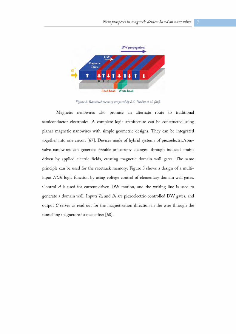


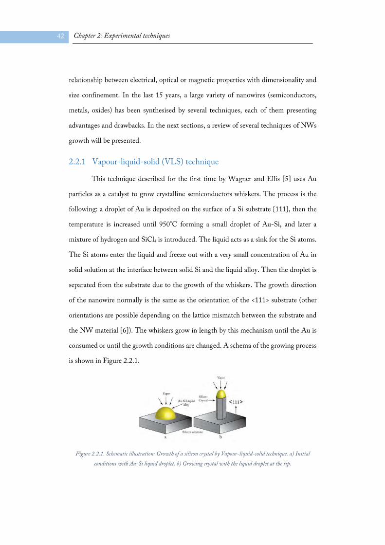

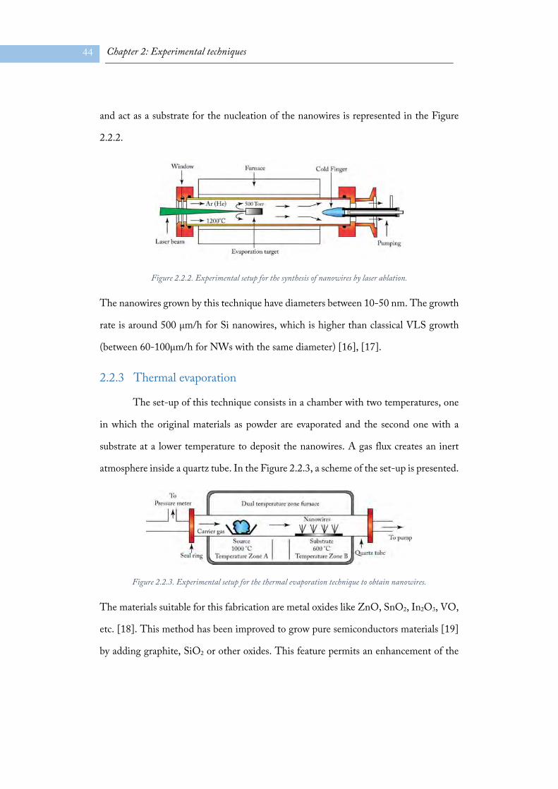


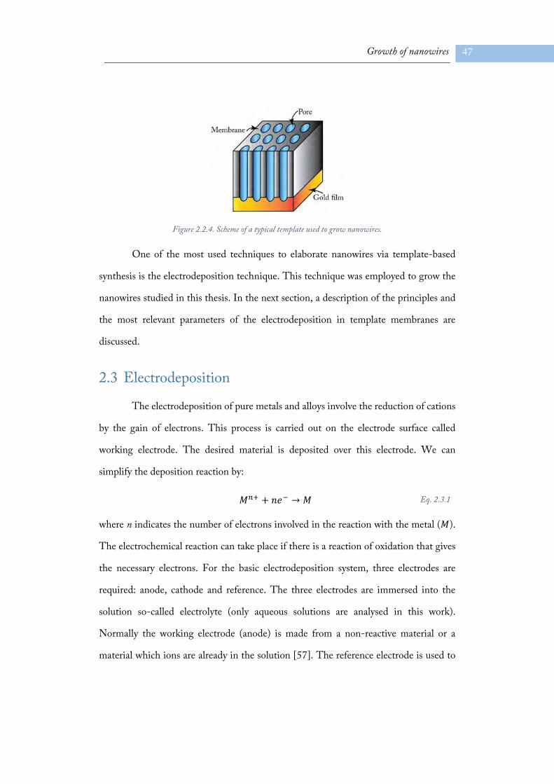


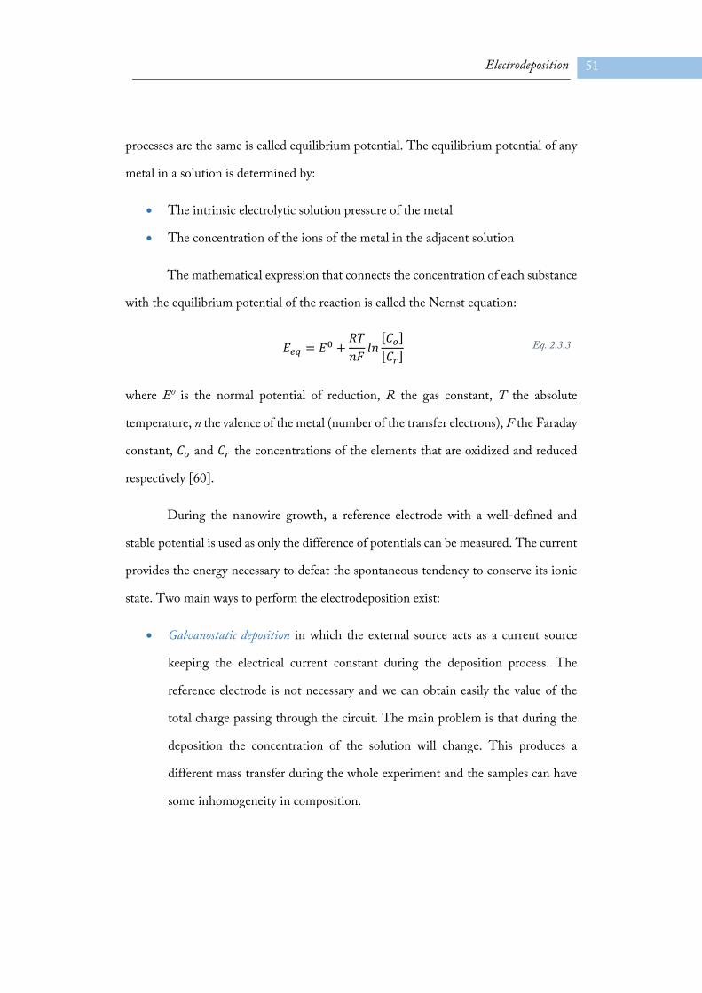


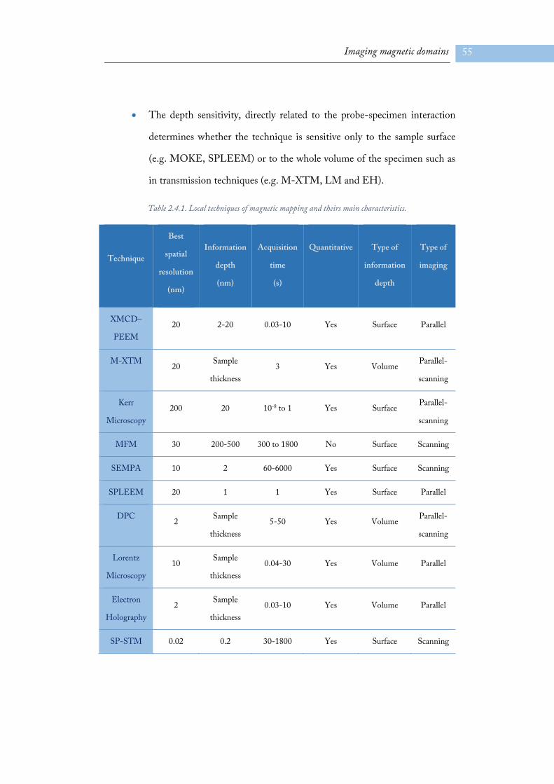


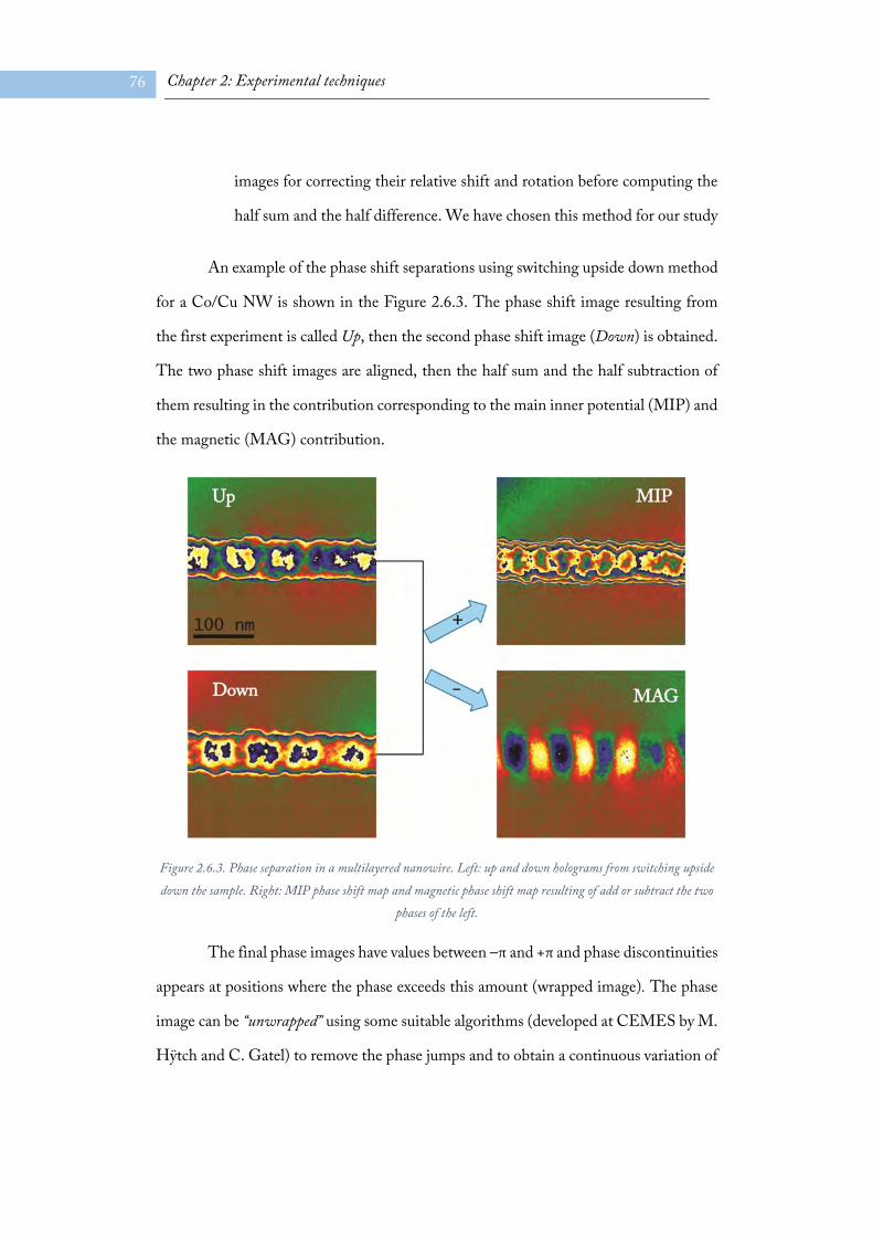


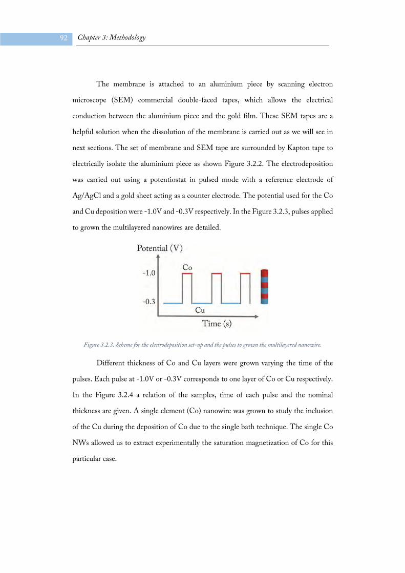


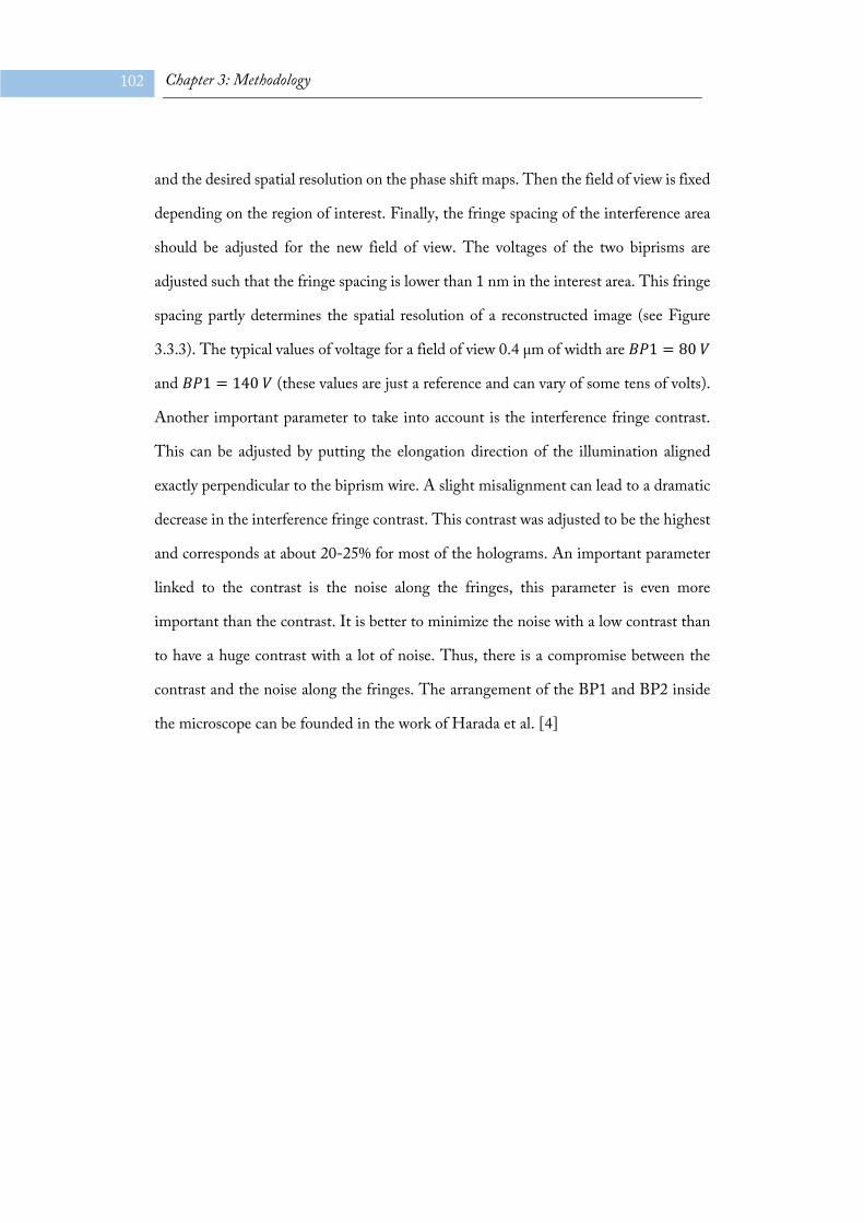


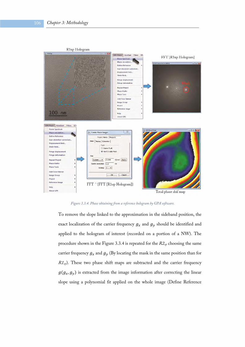


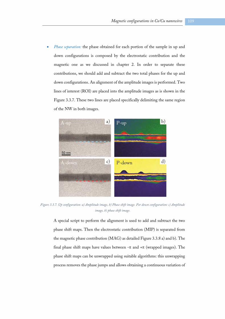

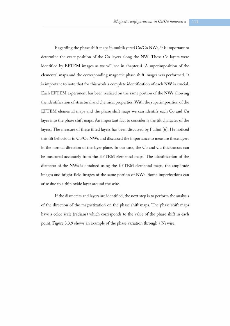
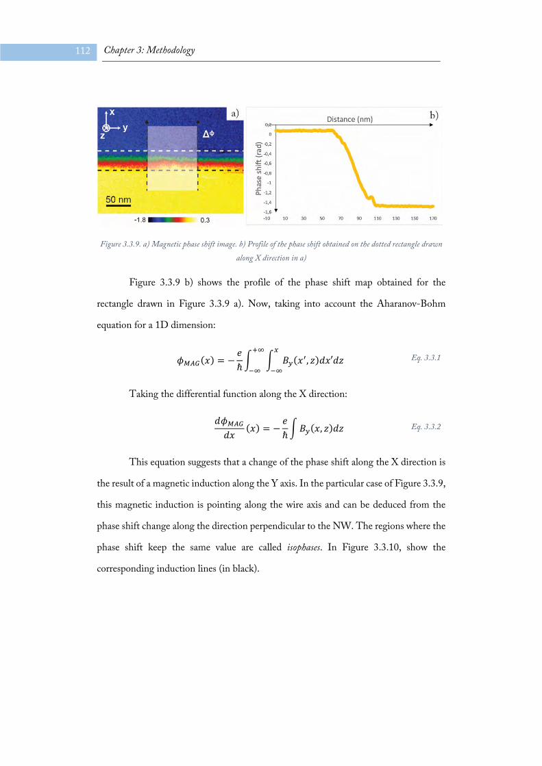
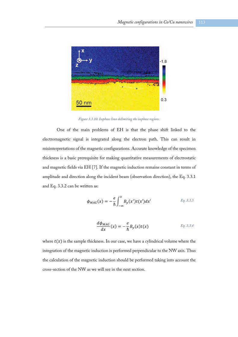
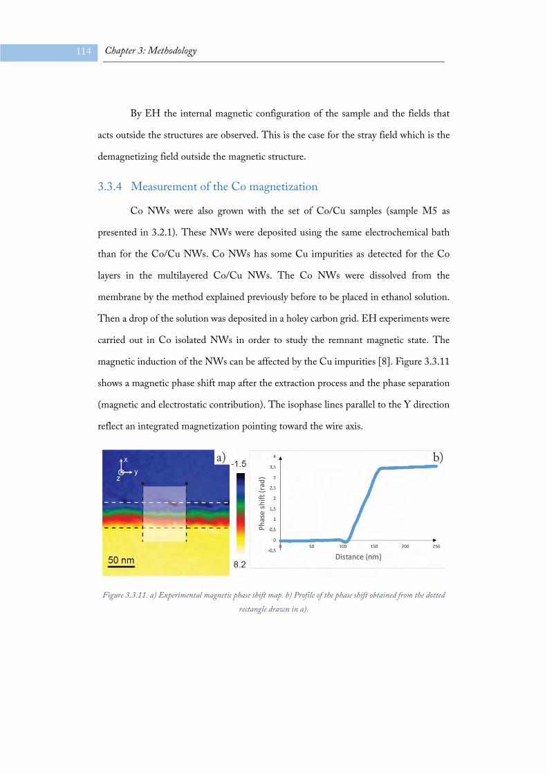


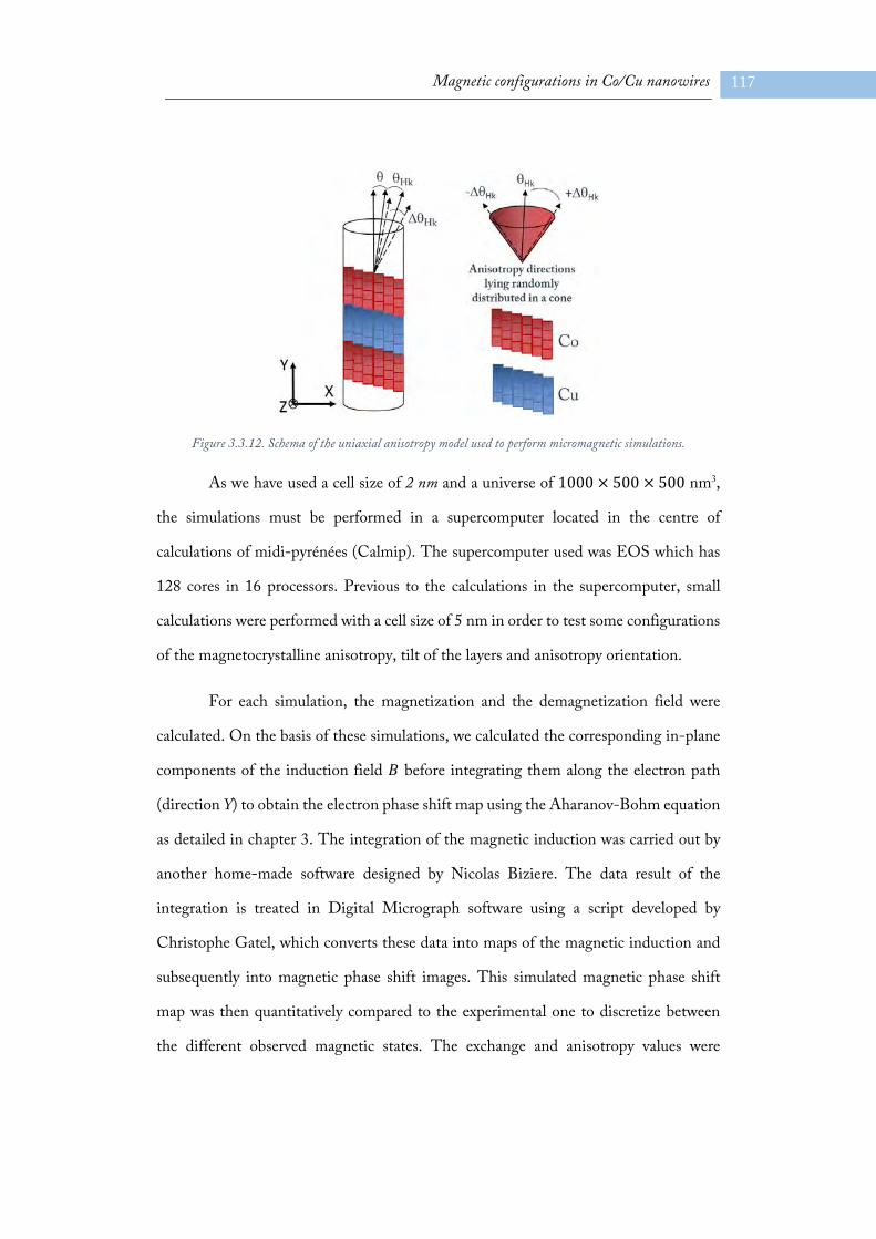


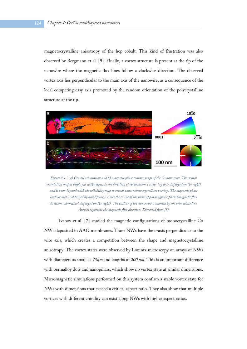


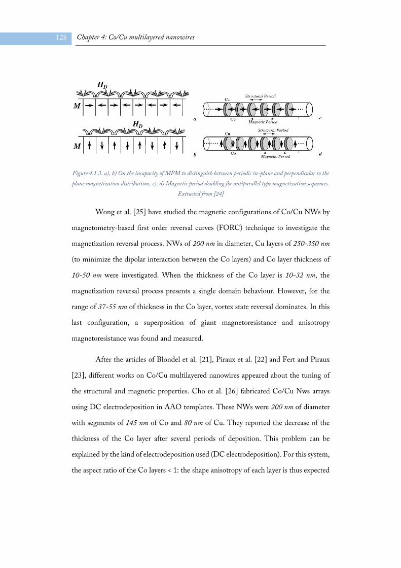


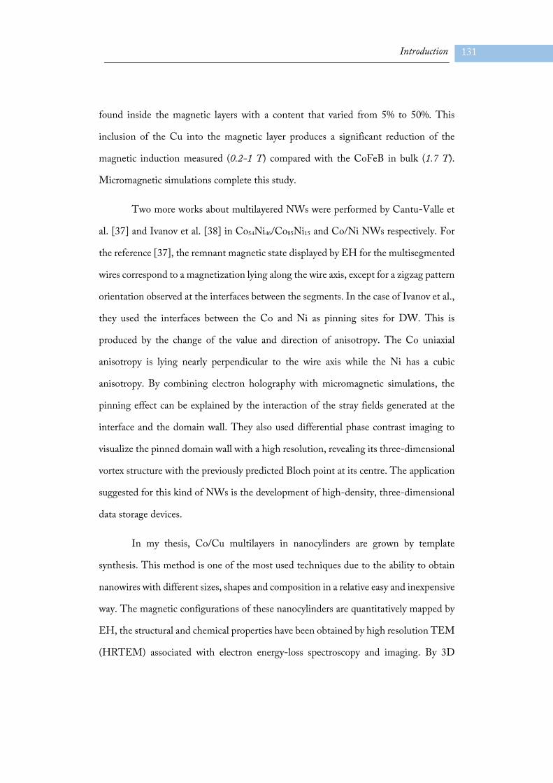
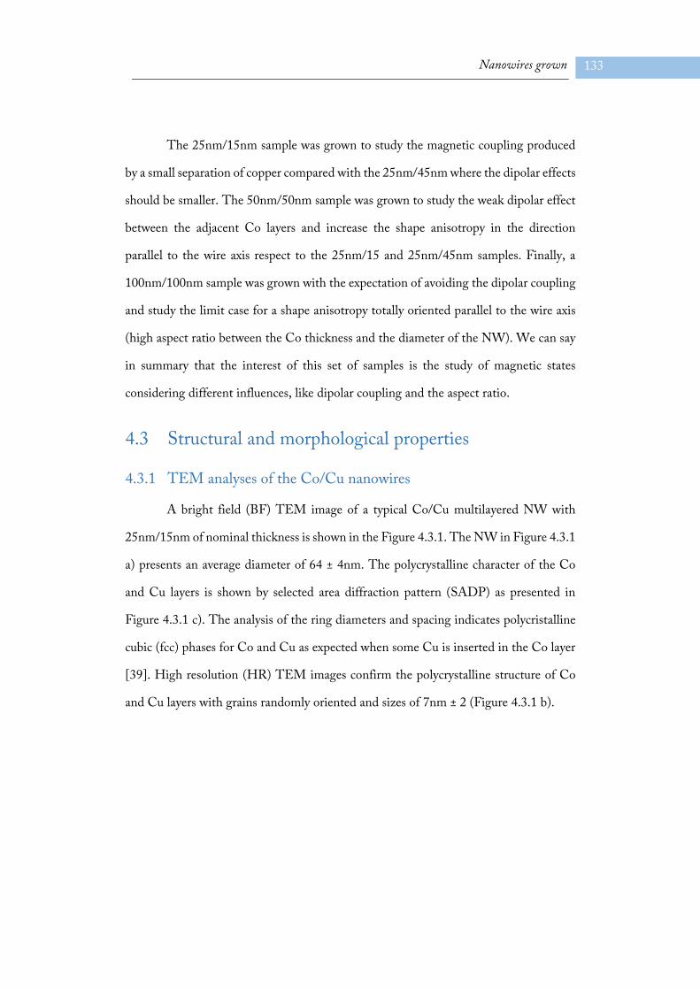


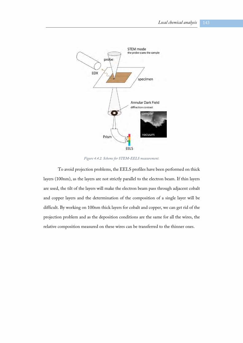
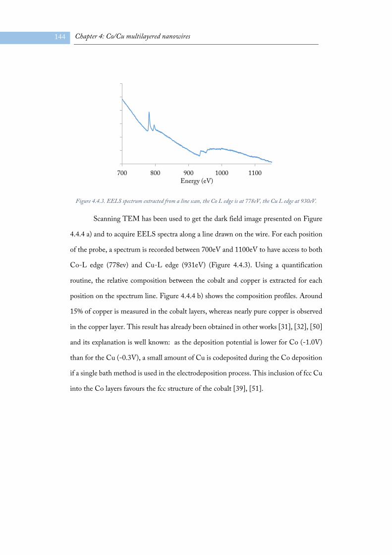
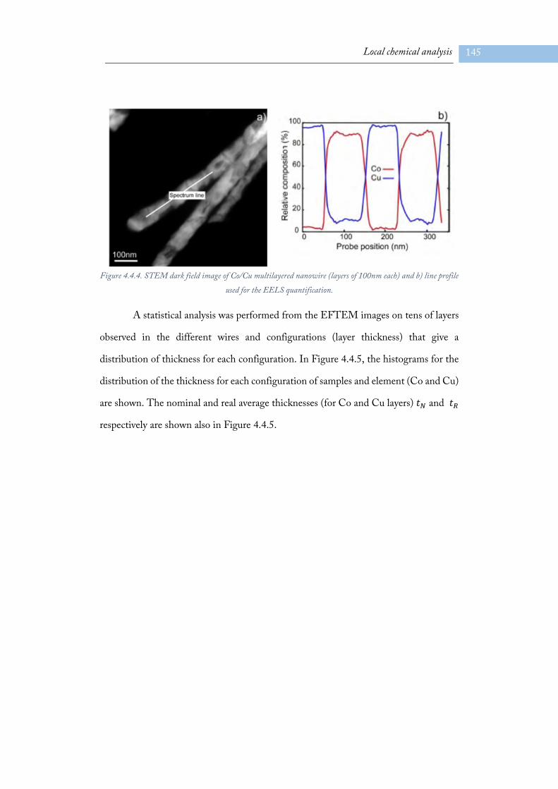

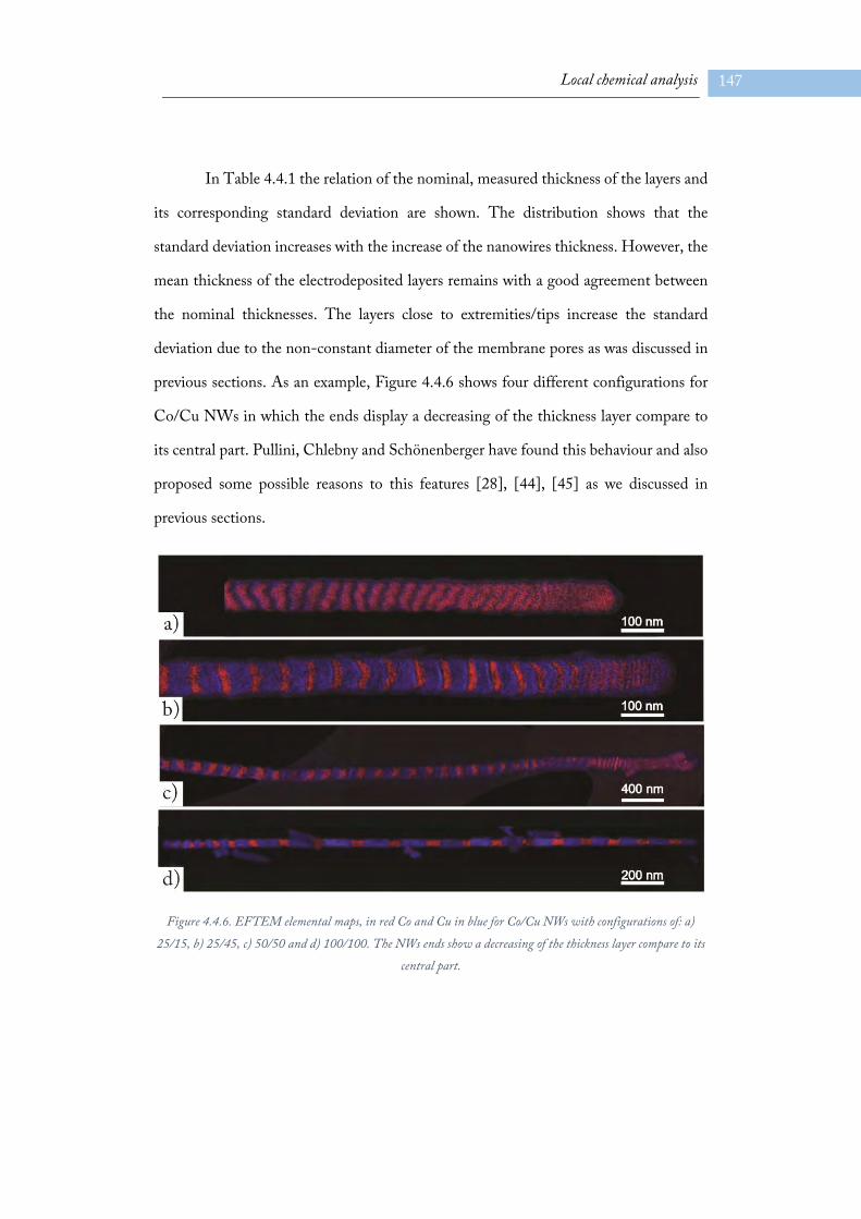

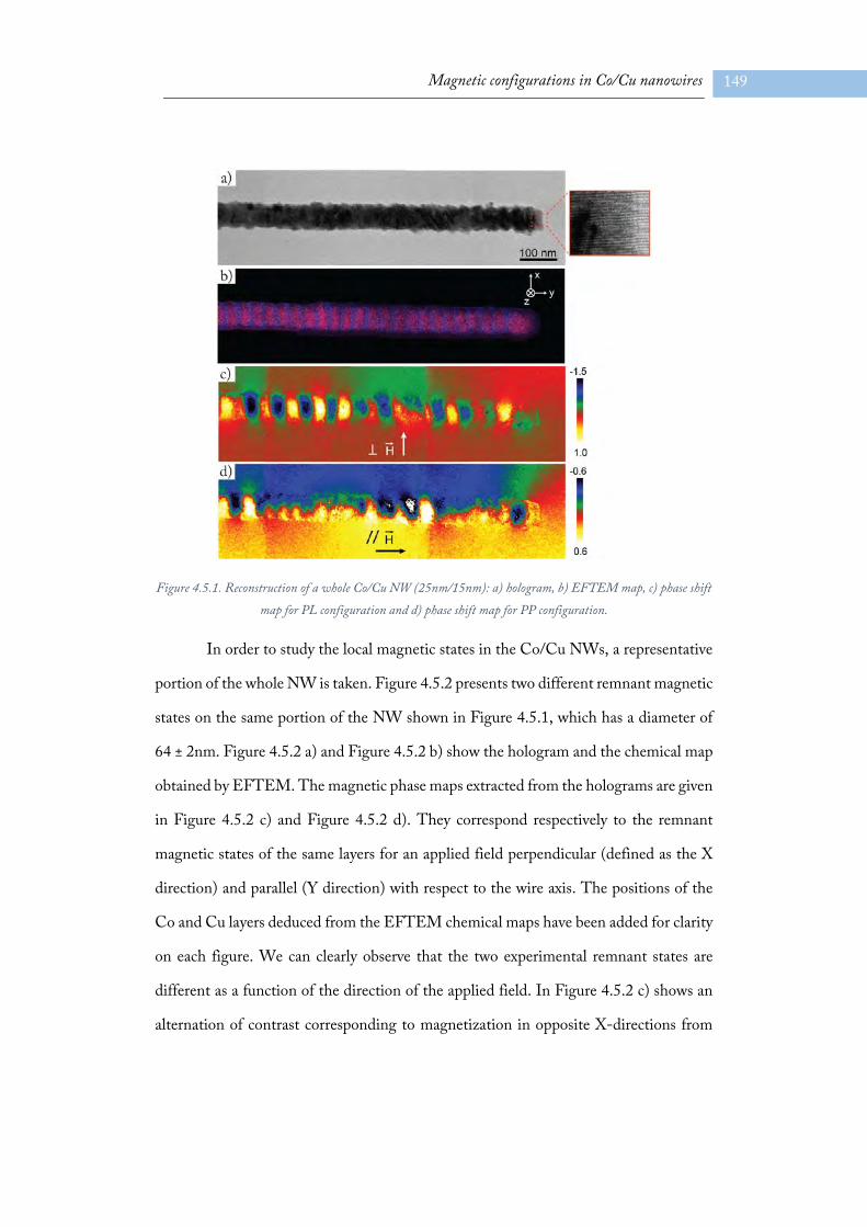


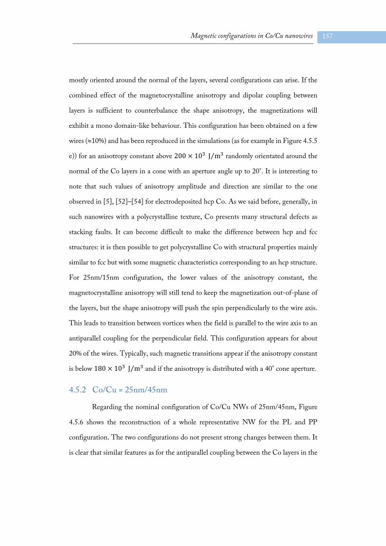


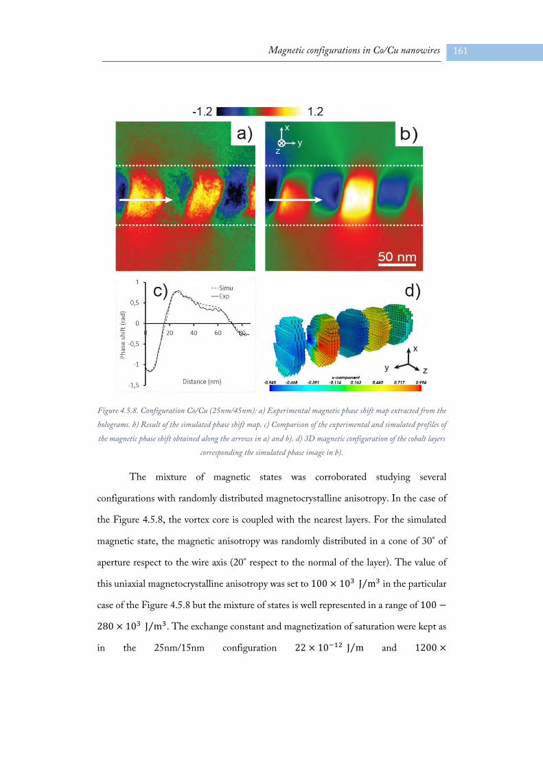

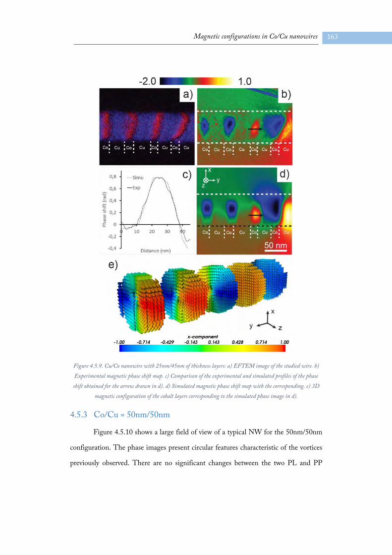


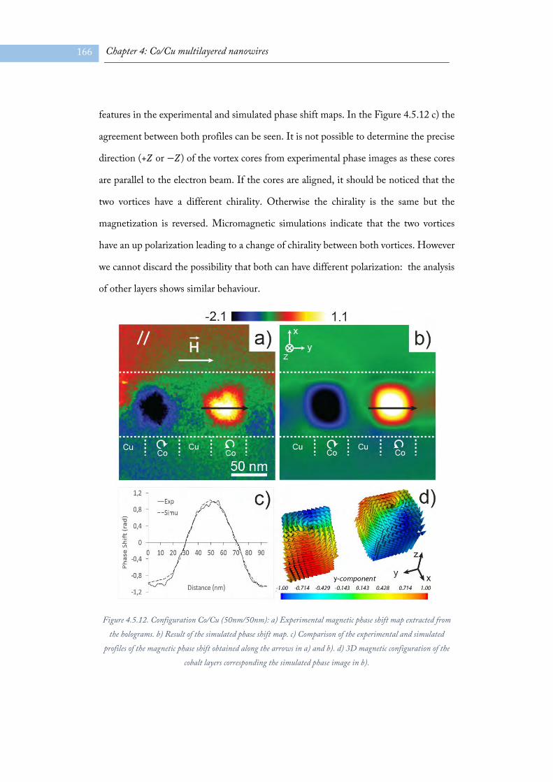
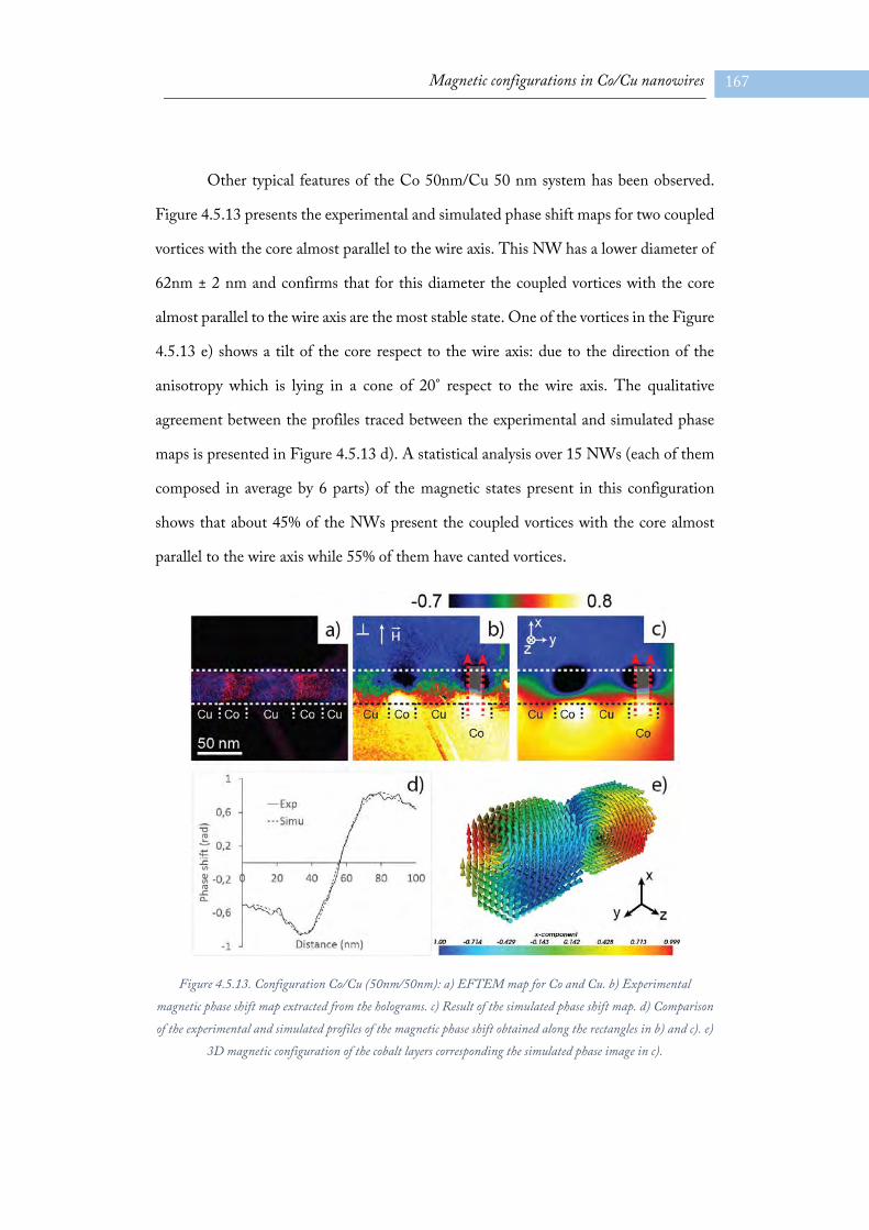


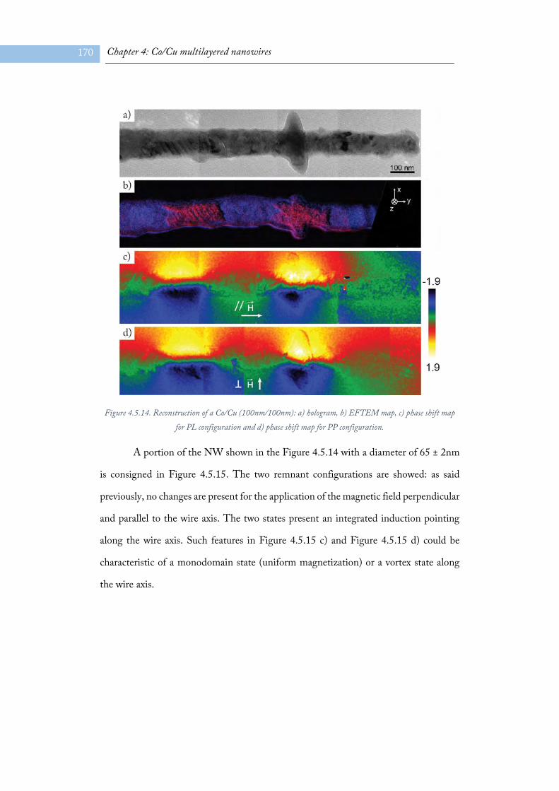


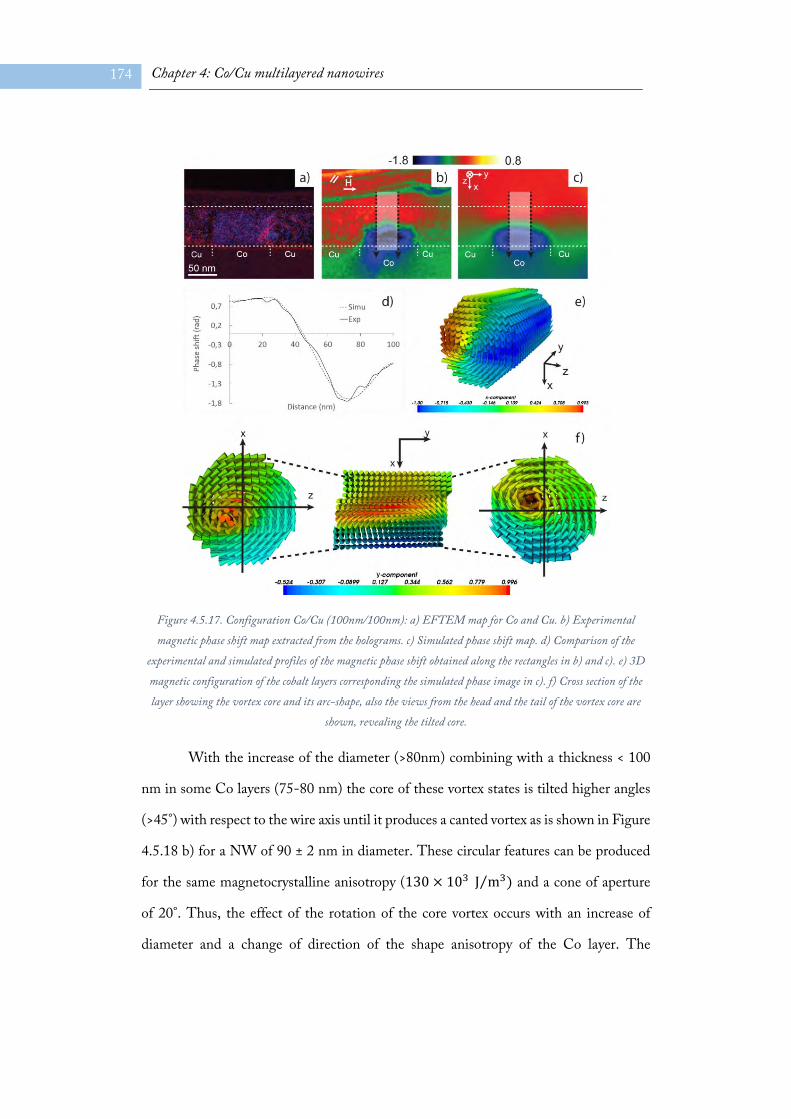

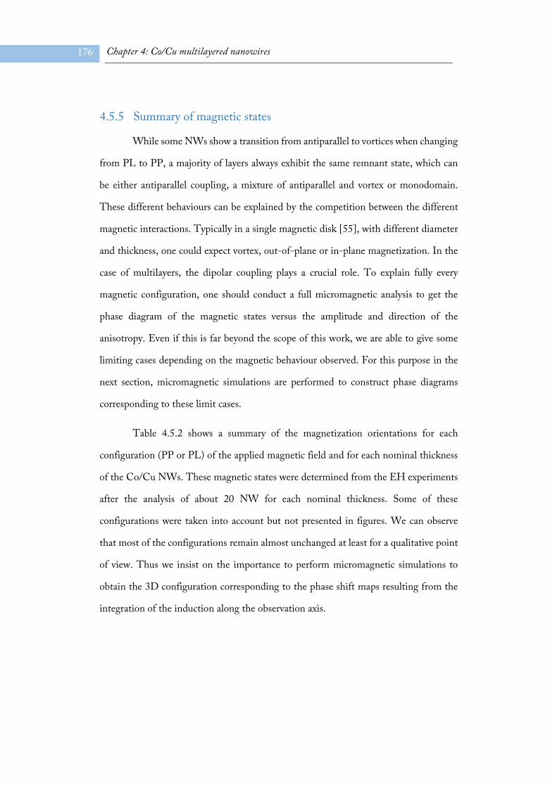
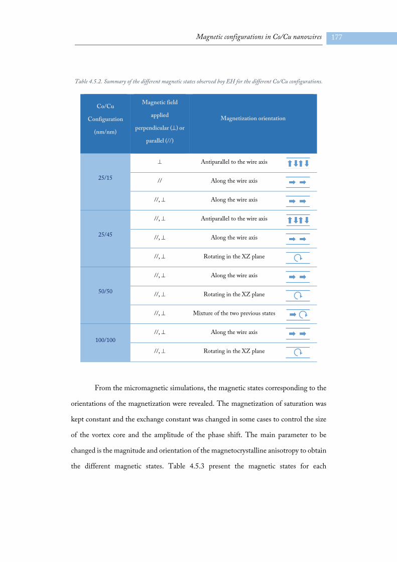


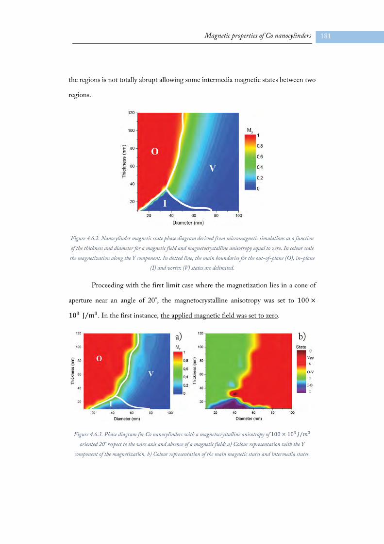

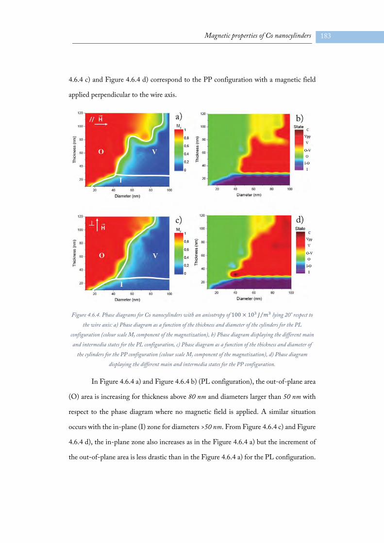


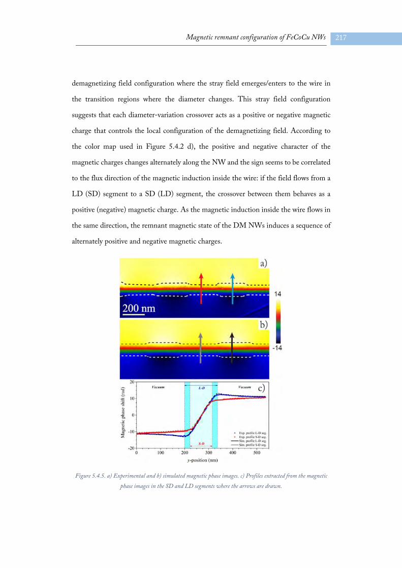


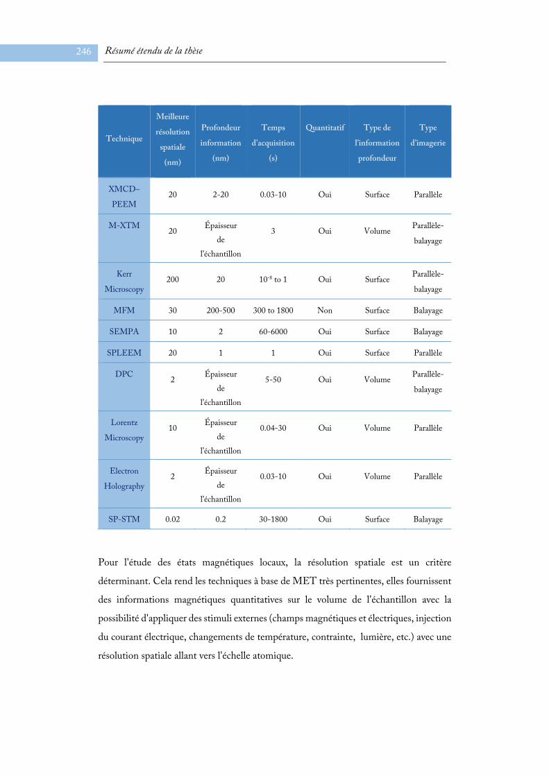
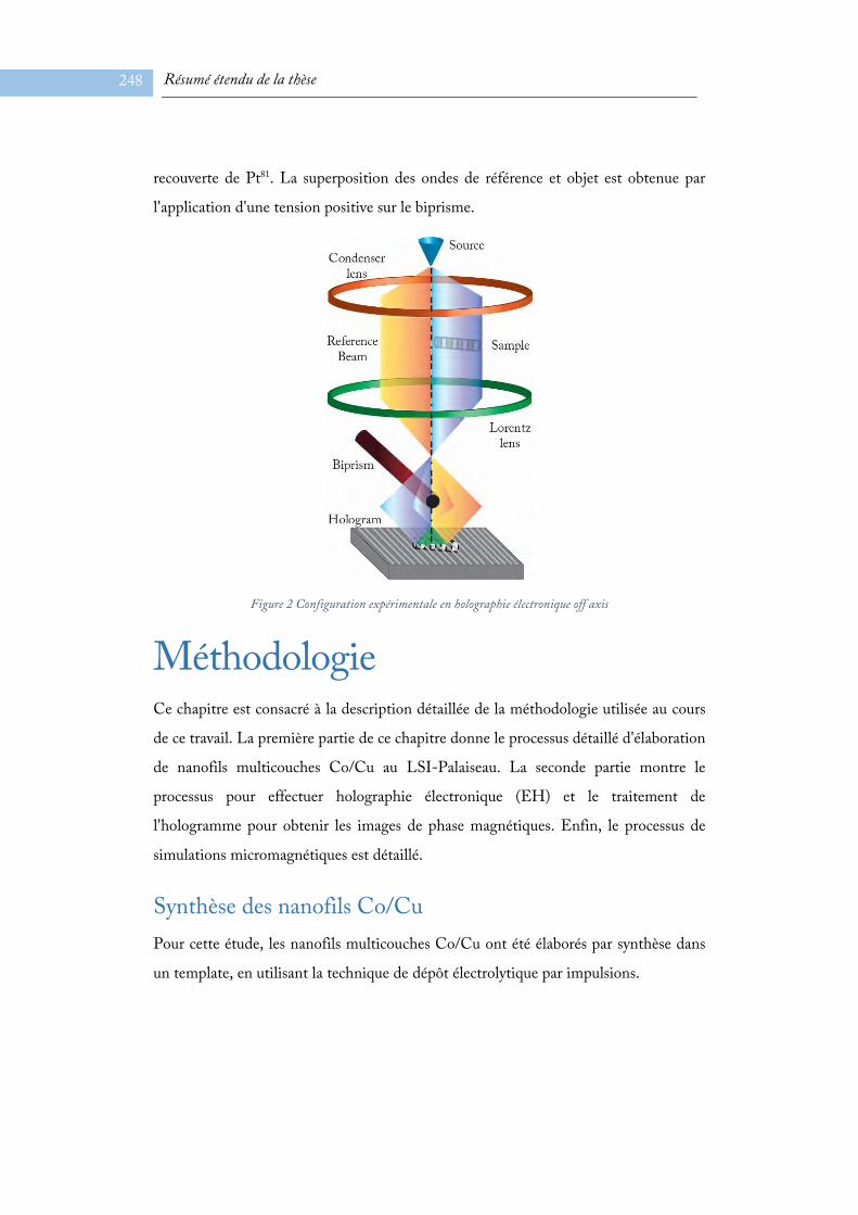


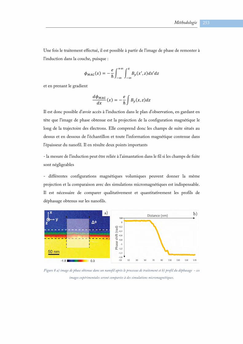


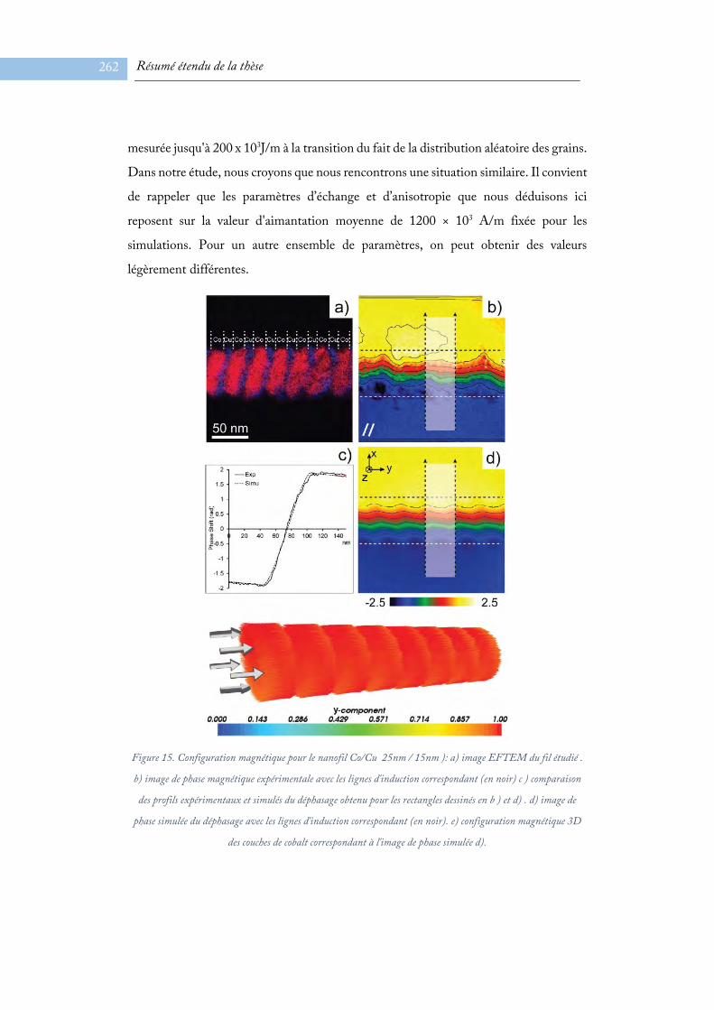


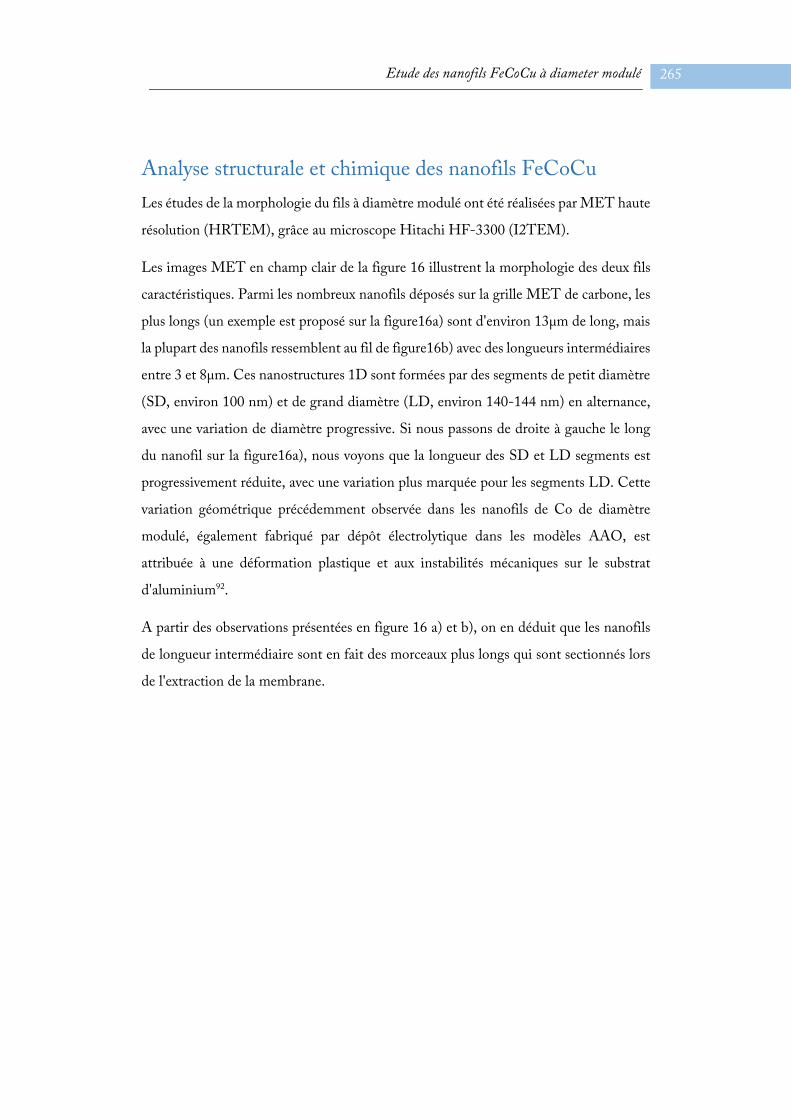


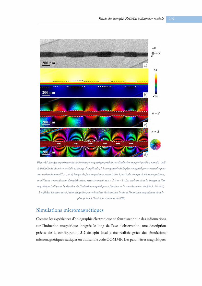

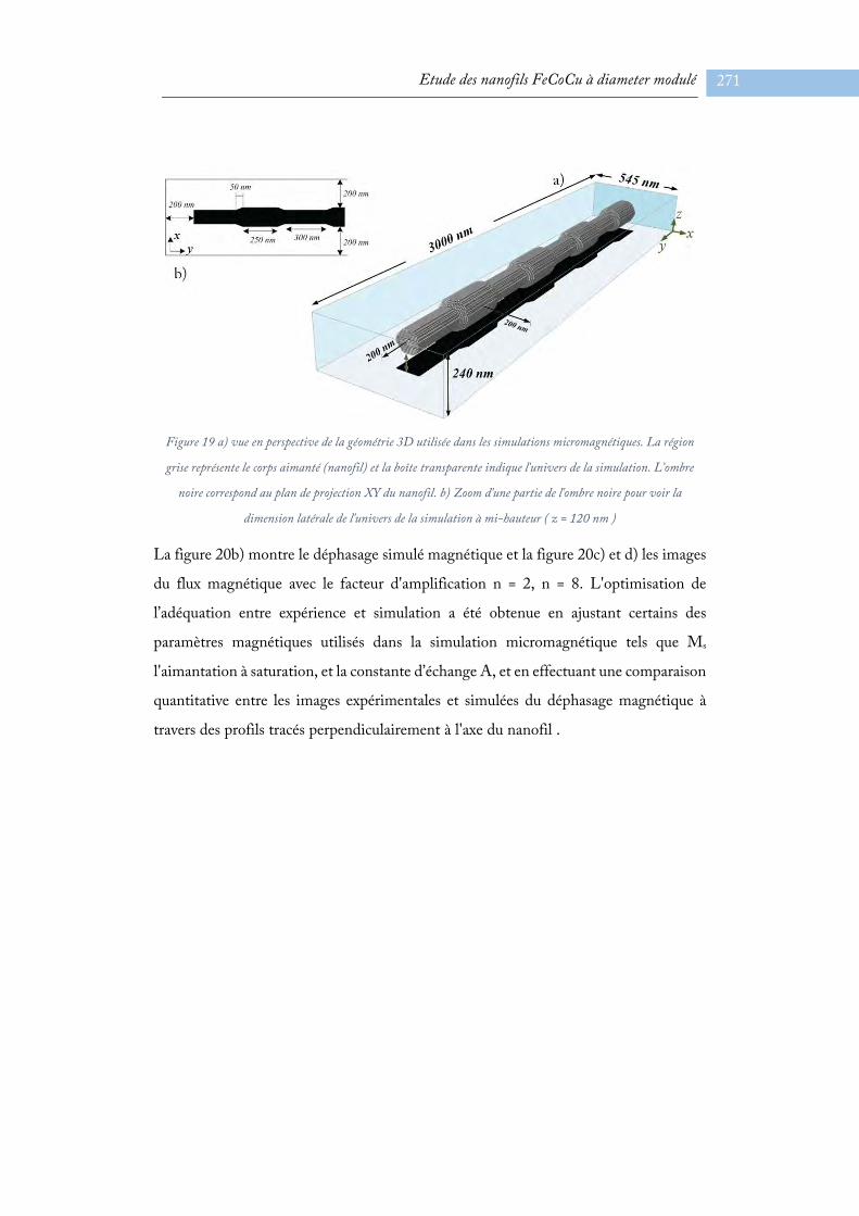
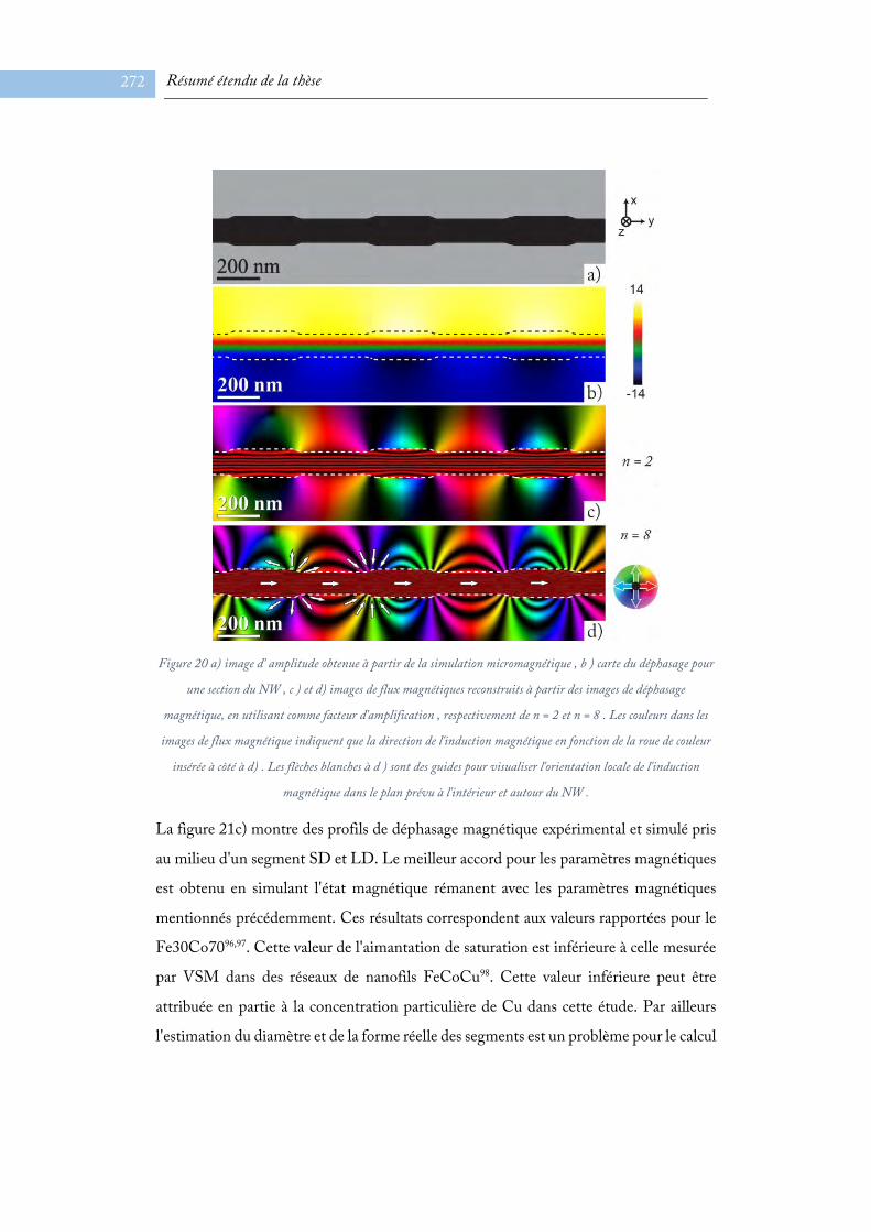


![5)µ4&thesesups.ups-tlse.fr/3630/1/2017TOU30112.pdf · driven cars [2], email SPAM filtering [3]… Moreover, it helped understand patterns and trends, for example, in stock exchange,](https://static.documents.pub/doc/80x56/5f558051d6c07568d91be5c2/54-driven-cars-2-email-spam-filtering-3-moreover-it-helped-understand.jpg)


![y .µ3 . } N $ s ù/à ¥3TX^2 (!E Ü 3« d...1 y .µ3 . } N $ s ù/à ¥3TX^2 (!E Ü 3« d »Ö 7ð÷à - ( ÷ ð çq 1 ; > < ª 2013 10 ]29 R2 y .µ4 Ë o 2 . } N $3 s ù ;](https://static.documents.pub/doc/80x56/5f248b4b493949624551284b/y-3-n-s-f-3tx2-e-oe-3-d-1-y-3-n-s-f-3tx2.jpg)


