Ordering Information General Information Safety Specification Absolute Maximum Ratings
Electrical Specification 2.56 A / 100 W 5.12 A / 200 W 7.69 A / 300 W 10.3 A / 400 W
Operating information Thermal Consideration Connections Mechanical Information Soldering Information Delivery Package Information Product Qualification Specification ........................................................... 21
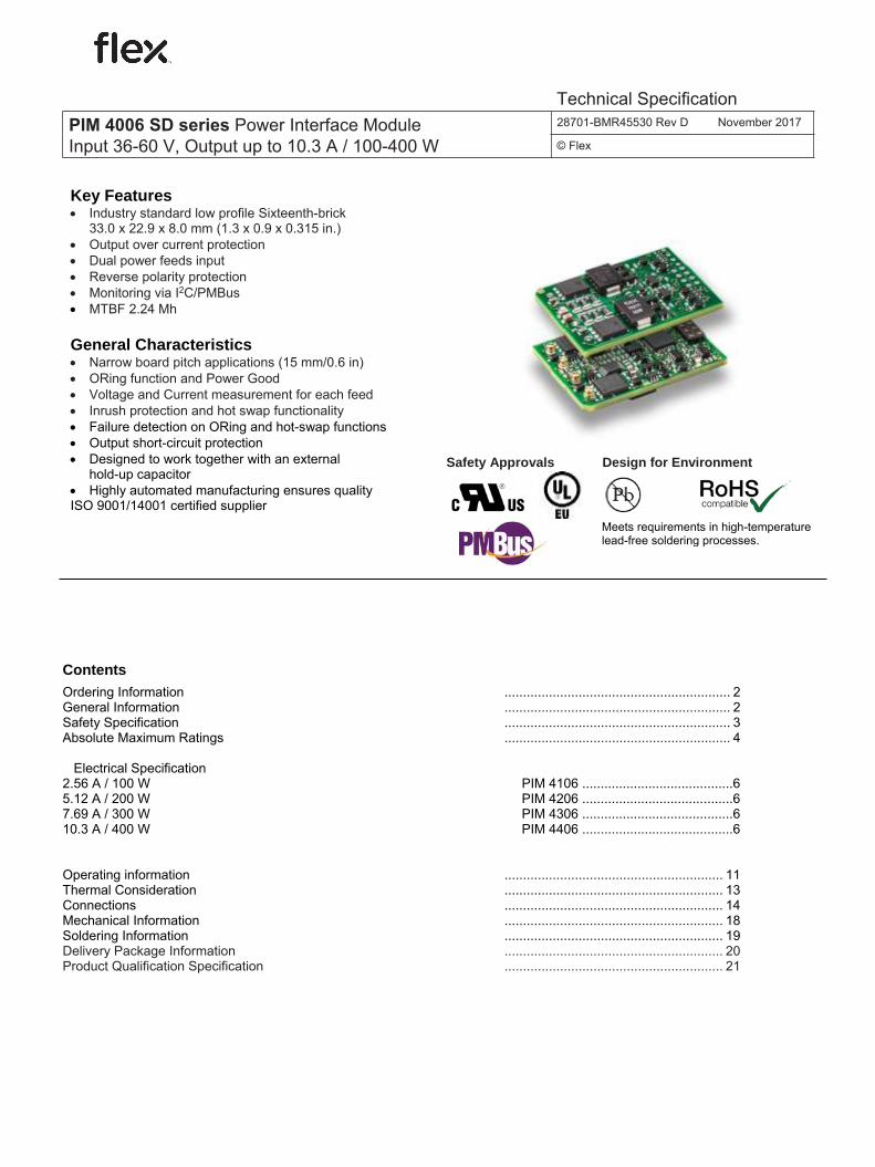
PIM 4006 SD series Power Interface ModuleInput 36-60 V, Output up to 10.3 A / 100-400 W
2 (4) Prepared (also subject responsible if other) No.
JID/S Marshall Wang 1/1301-BMR 455 00 Approved Checked Date Rev Reference
2017-11-15 B 0
Ordering Information
Product program Output
PIM 4106 2.56 A / 100 W
PIM 4206 5.12 A / 200 W
PIM 4306 7.69 A / 300 W
PIM 4406 10.3 A / 400 W
Product number and Packaging
PIM 4XXX n1n2n3n4
Options n1 n2 n3
Mounting
Function
Delivery package information
Options Description
n1
n2
n3
S D /B /C
Surface mount Standard config PMBus Tray Tape and Reel
Example a 200W. surface mounted, standard configuration with tray packaging would be PIM 4206SD/B.
* Standard variant (i.e. no option selected).
General Information
Reliability
The failure rate () and mean time between failures
(MTBF= 1/) is calculated at max output power and an
operating ambient temperature (TA) of +40°C. Flex Power Modules uses Telcordia SR-332 Issue 2 Method 1 to calculate the mean steady-state failure rate and standard
deviation (). Telcordia SR-332 Issue 2 also provides techniques to estimate the upper confidence levels of failure rates based on the mean and standard deviation. Mean steady-state failure rate, Std. deviation,
447 nFailures/h 53 nFailures/h
MTBF (mean value) for the PIM series = 2.24 Mh. MTBF at 90% confidence level = 1.94 Mh Compatibility with RoHS requirements
The products are compatible with the relevant clauses and requirements of the RoHS directive 2011/65/EU and have a maximum concentration value of 0.1% by weight in homogeneous materials for lead, mercury, hexavalent chromium, PBB and PBDE and of 0.01% by weight in homogeneous materials for cadmium. Exemptions in the RoHS directive utilized in Flex Power Modules products are found in the Statement of Compliance document. Flex Power Modules fulfills and will continuously fulfill all its obligations under regulation (EC) No 1907/2006 concerning the registration, evaluation, authorization and restriction of chemicals (REACH) as they enter into force and is through product materials declarations preparing for the obligations to communicate information on substances in the products.
Quality Statement
The products are designed and manufactured in an industrial environment where quality systems and methods like ISO 9000, Six Sigma, and SPC are intensively in use to boost the continuous improvements strategy. Infant mortality or early failures in the products are screened out and they are subjected to an ATE-based final test. Conservative design rules, design reviews and product qualifications, plus the high competence of an engaged work force, contribute to the high quality of the products. Warranty
Warranty period and conditions are defined in Flex Power Modules General Terms and Conditions of Sale. Limitation of Liability
The information and specifications in this technical specification is believed to be correct at the time of publication. However, no liability is accepted for inaccuracies, printing errors or for any consequences thereof. Flex reserves the right to change the contents of this technical specification at any time without prior notice.
PIM 4006 SD series Power Interface Module Input 36-60 V, Output up to 10.3 A / 100-400 W
3 (4) Prepared (also subject responsible if other) No.
JID/S Marshall Wang 1/1301-BMR 455 00 Approved Checked Date Rev Reference
2017-11-15 B 0
Safety Specification
General information
Flex Power Modules DC/DC converters and DC/DC regulators are designed in accordance with the safety standards IEC 60950-1, EN 60950-1 and UL 60950-1 Safety of Information Technology Equipment. IEC/EN/UL 60950-1 contains requirements to prevent injury or damage due to the following hazards:
Electrical shock
Energy hazards
Fire
Mechanical and heat hazards
Radiation hazards
Chemical hazards On-board DC/DC converters, Power interface modules and DC/DC regulators are defined as component power supplies. As components they cannot fully comply with the provisions of any safety requirements without “conditions of acceptability”. Clearance between conductors and between conductive parts of the component power supply and conductors on the board in the final product must meet the applicable safety requirements. Certain conditions of acceptability apply for component power supplies with limited stand-off (see Mechanical Information and Safety Certificate for further information). It is the responsibility of the installer to ensure that the final product housing these components complies with the requirements of all applicable safety standards and regulations for the final product. Component power supplies for general use should comply with the requirements in IEC/EN/UL 60950/1 Safety of Information Technology Equipment. Product related standards, e.g. IEEE 802.3af Power over Ethernet, and ETS-300132-2 Power interface at the input to telecom equipment, operated by direct current (dc) are based on IEC/EN/UL 60950-1 with regards to safety. Flex Power Modules DC/DC converters, Power interface modules and DC/DC regulators are UL 60950-1 recognized and certified in accordance with EN 60950-1. The flammability rating for all construction parts of the products meet requirements for V-0 class material according to IEC 60695-11-10, Fire hazard testing, test flames – 50 W horizontal and vertical flame test methods. Power interface modules
The product may provide basic or functional insulation between input and output according to IEC/EN/UL 60950-1 (see Safety Certificate), different conditions shall be met if the output of a basic or a functional insulated product shall be considered as safety extra low voltage (SELV).
For basic insulated products (see Safety Certificate) the output is considered as safety extra low voltage (SELV) if one of the following conditions is met:
The input source provides supplementary or double or reinforced insulation from the AC mains according to IEC/EN/UL 60950-1.
The input source provides functional or basic insulation from the AC mains and the product’s output is reliably connected to protective earth according to IEC/EN/UL 60950-1.
For functional insulated products (see Safety Certificate) the output is considered as safety extra low voltage (SELV) if one of the following conditions is met:
The input source provides double or reinforced insulation from the AC mains according to IEC/EN/UL 60950-1.
The input source provides basic or supplementary insulation from the AC mains and the product’s output is reliably connected to protective earth according to IEC/EN/UL 60950-1.
The input source is reliably connected to protective earth and provides basic or supplementary insulation according to IEC/EN/UL 60950-1 and the maximum input source voltage is 60 Vdc.
Galvanic isolation between input and output is verified in an electric strength test and the isolation voltage (Viso) meets the voltage strength requirement for basic insulation according to IEC/EN/UL 60950-1. It is recommended to use a slow blow fuse at the input of each product. If an input filter is used in the circuit the fuse should be placed in front of the input filter. In the rare event of a component problem that imposes a short circuit on the input source, this fuse will provide the following functions:
Isolate the fault from the input power source so as not to affect the operation of other parts of the system
Protect the distribution wiring from excessive current and power loss thus preventing hazardous overheating
Non-isolated DC/DC regulators
The DC/DC regulator output is SELV if the input source meets the requirements for SELV circuits according to IEC/EN/UL 60950-1.
PIM 4006 SD series Power Interface Module Input 36-60 V, Output up to 10.3 A / 100-400 W
TP1 Operating Temperature (see Thermal Consideration section) -40 +105 °C
TS Storage temperature -55 +125 °C
VI Input voltage -60 70 V
VI Input voltage, reverse polarity 60 V
VI Input voltage transient ANSI T1.315-2001 (R2006) 100 V
VI Common mode surge pulses (1.2/50 µs) IEC 61000-4-5 500 V
VIN2 PMBus input voltage -0.3 4.1 V
VSA0, VSA1 PMBus address pin-strap -0.3 VIN2 + 0.3 V
VPG Power good, open collector voltage 120 V
IPG Power good, sink current 100 mA
VSCL PMBus clock -0.3 VIN2 + 0.3 V
VSDA PMBus data -0.3 VIN2 + 0.3 V
VSALERT PMBus alert -0.3 VIN2 + 0.3 V
Stress in excess of Absolute Maximum Ratings may cause permanent damage. Absolute Maximum Ratings, sometimes referred to as no destruction limits, are normally tested with one parameter at a time exceeding the limits in the Electrical Specification. If exposed to stress above these limits, function and performance may degrade in an unspecified manner.
Fundamental Circuit Diagram
PIM 4006 SD series Power Interface Module Input 36-60 V, Output up to 10.3 A / 100-400 W
Note 1: It is recommended that a PMBus master reads back written data for verification i.e. do not rely on the ACK/NACK bit since this bit are as susceptible to errors as any other bit. However, under very rare operating conditions, it is possible to get intermittent read back failures. It is therefore recommended to implement error handling in the master that also deals with those situations.
PIM 4006 SD series Power Interface Module Input 36-60 V, Output up to 10.3 A / 100-400 W
Efficiency vs. load current and input voltage at TP1 = +25 C Note: max 10.3 A output current for PIM 4406 SD max 7.7 A output current for PIM 4306 SD max 5.2 A output current for PIM 4206 SD max 2.6 A output current for PIM 4106 SD
Dissipated power vs. load current and input voltage at TP1 = +25 °C Note: max 10.3 A output current for PIM 4406 SD max 7.7 A output current for PIM 4306 SD max 5.2 A output current for PIM 4206 SD max 2.6 A output current for PIM 4106 SD
Output Current Derating
Available load current vs. ambient air temperature and airflow at VI = 53 V. Note: max 10.3 A output current for PIM 4406 SD max 7.7 A output current for PIM 4306 SD max 5.2 A output current for PIM 4206 SD max 2.6 A output current for PIM 4106 SD
95
96
97
98
99
100
0 2 4 6 8 10
[%]
[A]
36 V
48 V
53 V
60 V
0
1
2
3
4
0 2 4 6 8 10
[W]
[A]
36 V
48 V
53 V
60 V
0
2
4
6
8
10
0 20 40 60 80 100
[A]
[°C]
3.0 m/s
2.0 m/s
1.5 m/s
1.0 m/s
0.5 m/s
Nat. Conv.
PIM 4006 SD series Power Interface Module Input 36-60 V, Output up to 10.3 A / 100-400 W
Start-up with minimum output capacitance Start-up with maximum output capacitance
PIM 4306 SD start-up of a DC/DC converter, PKB 4113C, using its RC function at: TP1 = +25 °C, output capacitance = 100 µF, PG activates the converter’s RC function, see Start-up Procedure section.
Top trace: output voltage (50 V/div.)) Second trace: input voltage (50 V/div.) Third trace: DC/DC output voltage (5 V/div.) Bottom trace: PG-signal (5 V/div.) (the sawtooth voltage originates from the DC/DC) Time scale: (10 ms/div.)
PIM 4306 SD start-up of a DC/DC converter, PKB 4113C, using its RC function at: TP1 = +25 °C, output capacitance = 750 µF, PG activates the converter’s RC function, see Start-up Procedure section.
Top trace: output voltage (50 V/div.)) Second trace: input voltage (50 V/div.) Third trace: DC/DC output voltage (5 V/div.) Bottom trace: PG-signal (5 V/div.) (the sawtooth voltage originates from the DC/DC) Time scale: (100 ms/div.)
ORing – feed switch ORing – short circuit of the feed with highest voltage
ORing at: TP1 = +25 °C, VIA = 54-52 V, VIB = 53 V, IO = 8.33 A electronic load
Top trace: input A current (5 A/div.). Second trace: input B current (5 A/div.). Third trace: input A voltage (2 V/div.). Bottom trace: input B voltage (2 V/div.). Time scale: (0.1 s/div.).
ORing functionality at: TP1 = +25 °C, VIA = 60 V (before short circuit), VIB = 40 V, output load = 10 kΩ
Top trace: input A current (1 A/div.) Second trace: output voltage (50 V/div.) Third trace: input A voltage (50 V/div.) Bottom trace: input B voltage (50 V/div.) Time scale: (10 ms/div.)
FET check
FET check at: TP1 = +25 °C, VIA = 53 V, VIB = 48 V, output capacitance = 100 µF, output loaded with a DC/DC converter, PKB 4113C, IDC/DC = 12 A See FET check section
Top trace: DC/DC output voltage (5 V/div.) Second trace: input current (2 A/div.) Third trace: output voltage (10 V/div.) Bottom trace: PG-signal (10 V/div.) Time scale: (0.1 ms/div.)
PIM 4006 SD series Power Interface Module Input 36-60 V, Output up to 10.3 A / 100-400 W
2 (7) Prepared (also subject responsible if other) No.
EABEFHJ 30/1301-BMR 455 30 Uen Approved Checked Date Rev Reference
EAB/FJB/GMF (Ksenia Harrisen) MICRF 2014-01-14 B
EMC Recommendations Recommendations for external components to meet the requirements according to EN55022, CISPR 22 and FCC part 15J class B (see test set up), when the PIM is used in conjunction with Flex BMR 456 0004 and BMR 457 0004 DC/DC converters.
Conducted EMI Input terminal peak value (typ)
in combination with BMR 456 0004 VI = 53 V, PO = 400 W, IBMR4560004 = 33 A C1 = 220 µF, C2 = 220 µF, C3 = 1500 µF, C4 = 100 nF, L1 = 22 µH, R3 = 1k Ω, R4 = not populated
in combination with BMR 457 0004 VI = 53 V, PO = 265W, IBMR4570004 = 21 A C1 = 220 µF, C2 = 330 µF, C3 = 1500 µF, C4 = 100 nF, L1 = 22 µH, R3 = 1k Ω, R4 = not populated
LISN
5 µH 50 R
DCPowerSource
rcvr
outin
5 µH 50 R
in LISN
rcvr
out-
+
PIMDC/DCConverter
ResistiveLoad
EMCReceiver
Computer
50 ohm input
Printed Circuit Board
Test set-up
Power Good and filter inductor When the PIM is used with a filter inductor, L1 in Typical Application Circuit diagram, special considerations must be made regarding the connection between the PG-output of the PIM and the RC-input of the DC/DC converter. During some modes of operation (e.g. input voltage transients) voltage ringing may appear across the filter inductor. This ringing may be substantial enough to cause either the DC/DC converter to momentarily turn off or cause excessive negative voltage on the RC-input if the PG-output is directly connected to the RC-input. A filter on the PG-signal (R3 and C4) can be used to remedy this problem. The resistance of R3 must be low enough to keep the voltage level on the RC-input below its turn-on threshold. A 1 kΩ resistor works well with BMR 456, BMR 457 and PKB-C. Clamping diodes across the filter inductor may also be used. The diode D1 in the Application Circuit diagram will prevent -OUT of the PIM from going more than a diode drop higher than -IN of the DC/DC converter. This will prevent the voltage on the RC-pin from going above the turn off threshold. The voltage on the RC-pin could still be negative if -OUT of the PIM goes below -IN of the DC/DC converter. Another diode, anti-parallel to D1, would solve this problem.
PIM 4006 SD series Power Interface Module Input 36-60 V, Output up to 10.3 A / 100-400 W
3 (7) Prepared (also subject responsible if other) No.
EABEFHJ 30/1301-BMR 455 30 Uen Approved Checked Date Rev Reference
EAB/FJB/GMF (Ksenia Harrisen) MICRF 2014-01-14 B
Operating information
Power Management Overview
This product is equipped with a PMBus interface. The product incorporates a range of readable and configurable power management features that are simple to implement with a minimum of external components. Additionally, the product includes protection features that continuously safeguard the load from damage due to unexpected system faults. The following product parameters can continuously be monitored by a host: input A voltage, input B voltage, ORed input voltage, input A current, input B current, output current, and internal junction temperature.
Input Voltage
The input voltage range 36 to 60 Vdc meets the requirements of the European Telecom Standard ETS 300 132-2 for normal input voltage range in -48 systems, -40.5 to -57.0 V.
A/B Feed ORing
Two MOSFETs (one ORing control) provide ORing of the input feeds. If a short is detected on one of the feeds the control circuit will detect reverse current and quickly turn the MOSFETs off. This feature also protects the product against reverse polarity up to 60 V. If a fuse blow is desired in case of wrong polarity place TVS diodes between negative and positive branch in both feeds. At high load operation the MOSFETs are operated at a low RDS(on) condition.
ORing and hot swap MOSFET short circuit check
A short circuited ORing or hot swap MOSFET can be detected by using the MFR_FETCHECK-command via the PMBus interface.
Hot Swap Functionality
The hot swap function is designed to control the inrush current to the downstream DC/DC converter. The level and duration of the inrush current complies with inrush current limits for PICMG 3.0 ATCA boards. Note: The hot swap circuit limits the output current during start up. Hence, the output cannot be loaded before its external filter capacitor has been charged (power good pin (PG) is asserted)
Start-up Procedure
The product follows a specific internal start-up procedure after power is applied to input A or input B:
1. When input A or input B reaches the turn on voltage level, the charging of the external filter capacitor starts.
2. When the output voltage is equal to the input voltage the power good pin (PG) is asserted.
3. The downstream DC/DC converter turns on when PG activates the converter’s RC function.
4. The DC/DC converter powers a step-down converter as supplies input 2.
5. After power is applied to input 2 the PMBus address (according to the pin-strap) is loaded.
Once this procedure is completed the product is ready to be loaded and accept commands via the PMBus interface, which will overwrite any default values used during the start-up procedure.
Power Good
The power good (PG) pin indicates that the output is ready to be loaded. An open collector turns on (sinks current) when the output voltage is equal to the voltage present on input A or input B. PG is referenced to –OUT.
PMBus, external power supply
The PMBus interface requires an external 3.3V power supply (+IN 2). ORing and hot swap will work without the external power supply but the PMBus communication will not.
PIM 4006 SD series Power Interface Module Input 36-60 V, Output up to 10.3 A / 100-400 W
4 (7) Prepared (also subject responsible if other) No.
EABEFHJ 30/1301-BMR 455 30 Uen Approved Checked Date Rev Reference
EAB/FJB/GMF (Ksenia Harrisen) MICRF 2014-01-14 B
Input Transient Over Voltage Protection
The product incorporates a transient voltage protector which will protect the product and the downstream DC/DC converter against over voltage transients exceeding 70 V. The transient voltage protector is rated for 1.5 kW peak pulse power with a breakdown voltage of 71 V. The product also handles transients of up to 100 V for 10 µs.
Over Voltage Protection (OVP)
The product includes over voltage limiting circuitry for protection of the load from continuous high voltage. When the input voltage exceeds 75 V the product will shut down. The product will resume normal operation automatically when the input voltage is within its specified range.
Over Temperature Protection (OTP)
The product includes over temperature limiting circuitry for protection of the load. When TP1 as defined in thermal consideration section exceeds 120 °C the product will shut down. The product will make continuous attempts to start up (non-latching mode) and resume normal operation automatically when the temperature has dropped > 10 °C below the temperature threshold.
Over Current Protection (OCP)
The product includes current limiting circuitry for protection at continuous overload. The output will abruptly be interrupted if the output overcurrent- or an internal component overpower thresholds are exceeded for a time longer than the stated fault response time.
PIM 4006 SD series Power Interface Module Input 36-60 V, Output up to 10.3 A / 100-400 W
5 (7) Prepared (also subject responsible if other) No.
EABEFHJ 30/1301-BMR 455 30 Uen Approved Checked Date Rev Reference
EAB/FJB/GMF (Ksenia Harrisen) MICRF 2014-01-14 B
Thermal Consideration
General
The products are designed to operate in different thermal environments and sufficient cooling must be provided to ensure reliable operation. For products mounted on a PCB without a heat sink attached, cooling is achieved mainly by conduction, from the pins to the host board, and convection, which is dependent on the airflow across the product. Increased airflow enhances the cooling of the product. The Output Current Derating graphs found in the Output section provides the available output current vs. ambient air temperature and air velocity at VI = 53 V A guard band of 5 °C is applied to the maximum recorded component temperatures when calculating output current derating curves. The product is tested on a 254 x 254 mm, 35 µm (1 oz.), 16-layer test board mounted vertically in a wind tunnel with a cross-section of 608 x 203 mm.
Definition of product operating temperature
The product operating temperature is used to monitor the temperature of the product, and proper thermal conditions can be verified by reading the temperature via PMBus. The temperature shall not exceed the maximum temperature in the table below. Temperatures above maximum TP1, is not allowed and may cause permanent damage.
Description Max Temp.
PMBus temperature TP1 = 105 ºC
Temperature position and air flow direction.
Top view
AIR FLOW
PIM 4006 SD series Power Interface Module Input 36-60 V, Output up to 10.3 A / 100-400 W
1 (4) Prepared (also subject responsible if other) No.
EABEFHJ/MICHORG 31/1301-BMR 455 30 Uen Approved Checked Date Rev Reference
EAB/FJB/GMF (Ksenia Harrisen) MICRF 2014-01-13 B
PMBus Interface
This product provides a PMBus digital interface that enables the user to monitor the input voltages, input currents and device temperature. The product can be used with any standard two-wire I2C or SMBus host device. In addition, the module is compatible with PMBus version 1.2. The product supports bus clock frequencies from 10 to 400 kHz. External pull-up resistors may be added to the PMBus.
Monitoring via PMBus
It is possible to monitor a variety of different parameters and status/fault flags through the PMBus interface. It is also possible to continuously monitor one or more of the below parameters: Monitored parameters
Feed A voltage
Feed B voltage
ORed input voltage
Feed A current
Feed B current
Output current
Internal junction temperature Monitored status/fault flags
FET check feed A fail
FET check feed B fail
PMBus Addressing
The PMBus address should be configured with resistors connected between the SA0/SA1 pins and the RTN pin, as shown in the figure below. Recommended resistor values for hard-wiring PMBus addresses are shown in the table. 1% tolerance resistors are required.
Schematic of connection of address resistor.
SA0 index RSA0 SA1 index RSA1
7 open 7 open
6 100 kΩ 6 100 kΩ
5 47 kΩ 5 47 kΩ
4 27 kΩ 4 27 kΩ
3 18 kΩ 3 18 kΩ
2 10 kΩ 2 10 kΩ
1 4.7 kΩ 1 4.7 kΩ
0 closed 0 closed
The PMBus address follows the equation below: Eq. 8 PMBus address (decimal) = 8 × (SA1 index) + (SA0 index)
Note: PMBus address = 127d for closed RSA0 and RSA1 The user can theoretically configure up to 64 unique PMBus addresses. The user shall also be aware of further limitations of the address space as stated in the SMBus Specification.
SA0 SA1
RTN
RSA1
RSA0
PIM 4006 SD series Power Interface Module Input 36-60 V, Output up to 10.3 A / 100-400 W
2 (4) Prepared (also subject responsible if other) No.
EABEFHJ/MICHORG 31/1301-BMR 455 30 Uen Approved Checked Date Rev Reference
EAB/FJB/GMF (Ksenia Harrisen) MICRF 2014-01-13 B
PMBus Commands
The product is PMBus compliant. The following table lists the implemented PMBus commands. For more detailed information see PMBus Power System Management Protocol Specification; Part I – General Requirements, Transport and Electrical Interface and PMBus Power System Management Protocol; Part II – Command Language.
Designation Cmd Impl
PMBUS_OPERATION 01h Yes
CLEAR_FAULTS 03h Yes
STATUS_BYTE 78h Yes
READ_VIN (LINEAR) 88h Yes
READ_IOUT (LINEAR) 8Ch Yes
READ_TEMPERATURE_1 (LINEAR) 8Dh Yes
PMBUS_REVISION 98h Yes
MFR_ID 99h Yes
MFR_MODEL 9Ah Yes
MFR_REVISION 9Bh Yes
MFR_LOCATION 9Ch Yes
MFR_DATE 9Dh Yes
MFR_SERIAL 9Eh Yes
MFR_READ_VINA (LINEAR) D3h Yes
MFR_READ_VINB (LINEAR) D4h Yes
MFR_READ_IINA (LINEAR) D6h Yes
MFR_READ_IINB (LINEAR) D7h Yes
MFR_FETCHECK D8h Yes
MFR_FETCHECKSTATUS D9h Yes Notes: Cmd is short for Command. Impl is short for Implemented. RW is short for Read Write access CLEAR_FAULTS only supports clearing of the CML bit. STATUS_BYTE only supports reading of the CML bit. LINEAR, value is represented in PMBus LINEAR format.
MFR_FETCHECK A read/write register to start a FET check operation. Write 55h followed by AAh to launch FET check on feed A. Write 56h followed by ABh to launch FET check on feed B.
Designation Bit
COMMAND KEY 0-7
MFR_FETCHECKSTATUS A read only register that displays current status.
Designation Bit
FEED_A_TESTING 0
FEED_B_TESTING 1
FEED_A_RECOVER 2
FEED_B_RECOVER 3
FEED_A_UV 4
FEED_B_UV 5
FEED_A_TEST_PASS 6
FEED_B_TEST_PASS 7
CMD_IGNORED 8
FEED_A_LOSS 9
FEED_B_LOSS 10
FEED_A_VALID 11
FEED_B_VALID 12
Reserved 13-15
MFR_FETCHECKSTATUS flag description
Designation Function
FEED_A_TESTING Asserted when a FET check is in progress on feed A. When asserted a new test cannot be started.
FEED_B_TESTING Asserted when a FET check is in progress on feed B. When asserted a new test cannot be started.
FEED_A_RECOVER Asserted for 1 s when a FET check on feed A has finished. When asserted a new test cannot be started.
FEED_B_RECOVER Asserted for 1 s when a FET check on feed B has finished. When asserted a new test cannot be started.
FEED_A_UV Asserted when the input voltage
PIM 4006 SD series Power Interface Module Input 36-60 V, Output up to 10.3 A / 100-400 W
3 (4) Prepared (also subject responsible if other) No.
EABEFHJ/MICHORG 31/1301-BMR 455 30 Uen Approved Checked Date Rev Reference
EAB/FJB/GMF (Ksenia Harrisen) MICRF 2014-01-13 B
on feed A goes below 45 V, de-asserted above 46 V. When asserted a new test cannot be started.
FEED_B_UV Asserted when the input voltage
on feed B goes below 45 V, de-asserted above 46 V. When asserted a new test cannot be started.
FEED_A_TEST_PASS Test result 1 = Test passed 0 = Test failed Valid when FEED_A_TESTING has de-asserted.
FEED_B_TEST_PASS Test result 1 = Test passed 0 = Test failed Valid when FEED_B_TESTING has de-asserted.
CMD_IGNORED Asserted when a FET check start command is given and any of bits 0 through 5 of MFR_FETCHECKSTATUS is asserted. The command is ignored. De-asserted when a FET check is successfully launched.
FEED_A_LOSS 1 = VINA < 36.9V 0 = VINA > 38.4V
FEED_B_LOSS 1 = VINB < 36.9V 0 = VINB > 38.4V
FEED_A_VALID 1 = FEED_A_TEST_PASS-bit contains a valid result. 0 = No FET-check has been performed after power on.
FEED_B_VALID 1 = FEED_B_TEST_PASS-bit contains a valid result. 0 = No FET-check has been performed after power on.
FET check
This function tests the hot swap and ORing FETs in one feed by briefly turning them off and measuring that the intermediate voltage between hot swap and ORing drops. If the intermediate voltage drops the corresponding FEED_x_TEST_PASS-bit is set else it is cleared. A FET check can only be launched when all of bits 0 through 5 of MFR_FETCHECKSTATUS are cleared. If any of these bits are set when a launch command is given the CMD_IGNORED-bit will be set and the command will be ignored. Recommended sequence to launch FET check and retrieve result.
Bits 0-5 == 0
Read MFR_FETCHECKSTATUS
No
Write MFR_FETCHECK = 55h
Yes
Read MFR_FETCHECK
== 55h No
Write MFR_FETCHECK = AAh
Read MFR_FETCHECK
Yes
== AAh No
Read MFR_FETCHECKSTATUS
Yes
CMD_IGNORED == 1
FEED_A_TESTING == 0
Yes
No
No
Valid result ready
Yes
PIM 4006 SD series Power Interface Module Input 36-60 V, Output up to 10.3 A / 100-400 W
1 (2) Prepared (also subject responsible if other) No.
EPETSCH 4/1301-BMR 455 30 Uen Approved Checked Date Rev Reference
EAB/FJB/GM [Ksenia Harrisen] See §1 2013-06-10 A F
Mechanical Information
All component placements – whether shown as physical components or symbolical outline – are for reference only and are subject to change throughout the product’s life cycle, unless explicitly described and dimensioned in this drawing.
PIM 4006 SD series Power Interface Module Input 36-60 V, Output up to 10.3 A / 100-400 W
The surface mount product is intended for forced convection or vapor phase reflow soldering in SnPb or Pb-free processes. The reflow profile should be optimised to avoid excessive heating of the product. It is recommended to have a sufficiently extended preheat time to ensure an even temperature across the host PWB and it is also recommended to minimize the time in reflow. A no-clean flux is recommended to avoid entrapment of cleaning fluids in cavities inside the product or between the product and the host board, since cleaning residues may affect long time reliability and isolation voltage.
General reflow process specifications SnPb eutectic Pb-free
Average ramp-up (TPRODUCT) 3°C/s max 3°C/s max
Typical solder melting (liquidus) temperature
TL 183°C 221°C
Minimum reflow time above TL 60 s 60 s
Minimum pin temperature TPIN 210°C 235°C
Peak product temperature TPRODUCT 225°C 260°C
Average ramp-down (TPRODUCT) 6°C/s max 6°C/s max
Maximum time 25°C to peak 6 minutes 8 minutes
TPRODUCT maximum TPIN minimum
Time
Pin profile
Product profile
TL
Time in reflow
Time in preheat / soak zone
Time 25°C to peak
Temperature
Minimum Pin Temperature Recommendations
Pin number 3 & 4 are chosen as reference locations for the minimum pin temperature recommendation since these will likely be the coolest solder joint during the reflow process.
SnPb solder processes
For SnPb solder processes, a pin temperature (TPIN) in excess of the solder melting temperature, (TL, 183°C for Sn63Pb37) for more than 60 seconds and a peak temperature of 220°C is recommended to ensure a reliable solder joint. For dry packed products only: depending on the type of solder paste and flux system used on the host board, up to a recommended maximum temperature of 245°C could be used, if the products are kept in a controlled environment (dry pack handling and storage) prior to assembly.
Lead-free (Pb-free) solder processes
For Pb-free solder processes, a pin temperature (TPIN) in excess of the solder melting temperature (TL, 217 to 221°C for SnAgCu solder alloys) for more than 60 seconds and a peak temperature of 245°C on all solder joints is recommended to ensure a reliable solder joint.
Maximum Product Temperature Requirements
Top of the product PWB near pin 12 is chosen as reference locations for the maximum (peak) allowed product temperature (TPRODUCT) since these will likely be the warmest part of the product during the reflow process.
SnPb solder processes
For SnPb solder processes, the product is qualified for MSL 1 according to IPC/JEDEC standard J-STD-020C. During reflow TPRODUCT must not exceed 225 °C at any time.
Pb-free solder processes
For Pb-free solder processes, the product is qualified for MSL 3 according to IPC/JEDEC standard J-STD-020C. During reflow TPRODUCT must not exceed 260 °C at any time.
Dry Pack Information
Products intended for Pb-free reflow soldering processes are delivered in standard moisture barrier bags according to IPC/JEDEC standard J-STD-033 (Handling, packing, shipping and use of moisture/reflow sensitivity surface mount devices). Using products in high temperature Pb-free soldering processes requires dry pack storage and handling. In case the products have been stored in an uncontrolled environment and no longer can be considered dry, the modules must be baked according to J-STD-033. Thermocoupler Attachment
Pin 3 & 4 for measurement of minimum Pin (solder joint) temperature TPIN
Pin 12 for measurement of maximum Product Temperature TPRODUCT
PIM 4006 SD series Power Interface Module Input 36-60 V, Output up to 10.3 A / 100-400 W
Vibration, broad band random IEC 60068-2-64 Fh, method 1 Frequency Spectral density Duration
10 to 500 Hz 0.07 g2/Hz 10 min in each direction
Notes 1 Only for products intended for reflow soldering (surface mount products) 2 Only for products intended for wave soldering (plated through hole products)
PIM 4006 SD series Power Interface Module Input 36-60 V, Output up to 10.3 A / 100-400 W