UCD9080www.ti.com................................................................................................................................................... SLVS692E–SEPTEMBER 2006–REVISED MAY 2008
8-CHANNEL POWER-SUPPLY SEQUENCER AND MONITOR
• Telecommunications Switches234• Single Supply Voltage: 3.3 V• Servers• Low Power Consumption• Networking Equipment• Sequences and Monitors up to Eight Voltage• Test EquipmentRails• Any System Requiring Sequencing of Multiple• Rail Voltages Sampled Every 50 µs With
Voltage Rails3.2-mV Resolution• Four Configurable Digital Outputs for
Power-On Reset and Other FunctionsThe UCD9080 power-supply sequencer controls the• Configurable Rail-Enable Output Polarityenable sequence of up to eight independent voltage
• Flexible Rail Sequencing: Timeline (ms), rails and provides four general-purpose digitalParent Rail Regulation Window, Parent Rail outputs. The device operates from a 3.3-V supply,Achieving Defined Threshold provides 3.2-mV resolution of voltage rails, and
requires no external memory or clock. The UCD9080• Under- and Overvoltage Thresholds: Settablemonitors the voltage rails independently at more thanPer-Raila 20-kHz rate and has a high degree of rail sequence• Regulation Expiration Time: Settable Per-Rail and rail error-response configurability. The
• Flexible Rail Shutdown: Parent Rail Shutdown sequencing of rails can be based on time or on timeCan Shut Down Child Rails, Independent Rail in conjunction with other rails achieving regulation orConfiguration a voltage threshold. In addition, each rail is monitored
for undervoltage and overvoltage glitches and• Per-Rail Alarm Conditions, With Timestamp:thresholds. Each rail the UCD9080 monitors can beUnder- and Overvoltage Glitch, Sustained configured to shut down a user-defined set of otherUnder- and/or Overvoltage, Rail Did Not Start rails, and alarm conditions are monitored on a per-rail
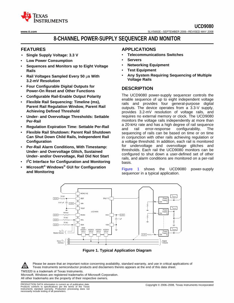
• I2C Interface for Configuration and Monitoring basis.• Microsoft® Windows® GUI for Configuration Figure 1 shows the UCD9080 power-supply
and Monitoring sequencer in a typical application.
Figure 1. Typical Application Diagram
1
Please be aware that an important notice concerning availability, standard warranty, and use in critical applications ofTexas Instruments semiconductor products and disclaimers thereto appears at the end of this data sheet.
2TMS320 is a trademark of Texas Instruments.3Microsoft, Windows are registered trademarks of Microsoft Corporation.4All other trademarks are the property of their respective owners.
UCD9080SLVS692E–SEPTEMBER 2006–REVISED MAY 2008................................................................................................................................................... www.ti.com
These devices have limited built-in ESD protection. The leads should be shorted together or the device placed in conductive foamduring storage or handling to prevent electrostatic damage to the MOS gates.
For the most current package and ordering information, see the Package Option Addendum at the end of thisdocument, or see the TI Web site at www.ti.com.
VALUE UNITVoltage applied from VCC to VSS –0.3 to 4.1 VVoltage applied to any pin (2) –0.3 to VCC + 0.3 VDiode current at any device terminal ±2 mA
Tstg Storage temperature –40 to 85 °C
(1) Stresses beyond those listed under absolute maximum ratings may cause permanent damage to the device. These are stress ratingsonly and functional operation of the device at these or any other conditions beyond those indicated under recommended operatingconditions is not implied. Exposure to absolute-maximum-rated conditions for extended periods may affect device reliability.
(2) All voltages referenced to VSS.
MIN NOM MAX UNITSupply voltage during operation 3 3.3 3.6
VCC VSupply voltage during configuration changes 3 3.3 3.6
TA Operating free-air temperature range –40 85 °C
These specifications are over recommended ranges of supply voltage and operating free-air temperature, unless otherwisenoted
PARAMETER TEST CONDITIONS MIN NOM MAX UNIT
SUPPLY CURRENT
Supply current into VCC, excluding externalIS TA = 25°C 3 4 mAcurrent
IC Supply current during configuration 3.6 V 3 7 mA
STANDARD INPUTS (RST, TEST)
VIL Low-level input voltage VCC = 3 V VSS VSS + 0.6 V
VIH High-level input voltage VCC = 3 V 0.8 VCC VCC V
UCD9080www.ti.com................................................................................................................................................... SLVS692E–SEPTEMBER 2006–REVISED MAY 2008
ELECTRICAL CHARACTERISTICS (continued)These specifications are over recommended ranges of supply voltage and operating free-air temperature, unless otherwisenoted
IOH(max) = –1.5 mA, (4) VCC = 3 V VCC – 0.25 VCCVOH High-level output voltage V
IOH(max) = –6 mA, (5) VCC = 3 V VCC – 0.6 VCC
IOH(max)= –1.5 mA, (4) VCC = 3 V VSS VSS + 0.25VOL Low-level output voltage V
IOH(max) = –6 mA, (5) VCC = 3 V VSS VSS + 0.6
Ilkg High-impedance leakage current VCC = 3 V ±50 nA
(1) Not production tested. Limits verified by design.(2) The current consumption of the brownout module is already included in the ICC current-consumption data.(3) During power up, device initialization starts subsequent to a period of td(BOR) after VCC = V(B_IT–) + Vhys(B_IT–).(4) The maximum total current, IOHmax and IOLmax, for all outputs combined, should not exceed ±12 mA to hold the maximum voltage drop
specified.(5) The maximum total current, IOHmax and IOLmax, for all outputs combined, should not exceed ±48 mA to hold the maximum voltage drop
specified.
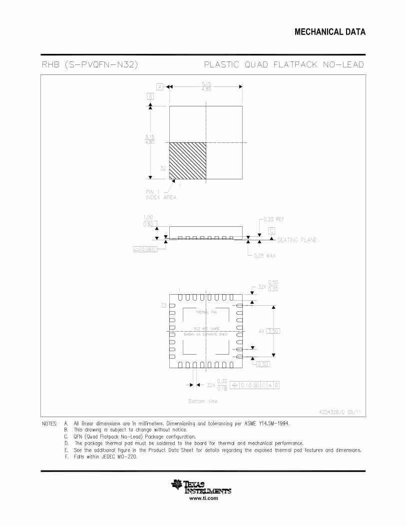
The UCD9080 is compatible with 3.3-V IO ports of microcontrollers, TMS320™ DSP family as well as ASICs.The UCD9080 is available in a plastic 32-pin QFN package (RHB).
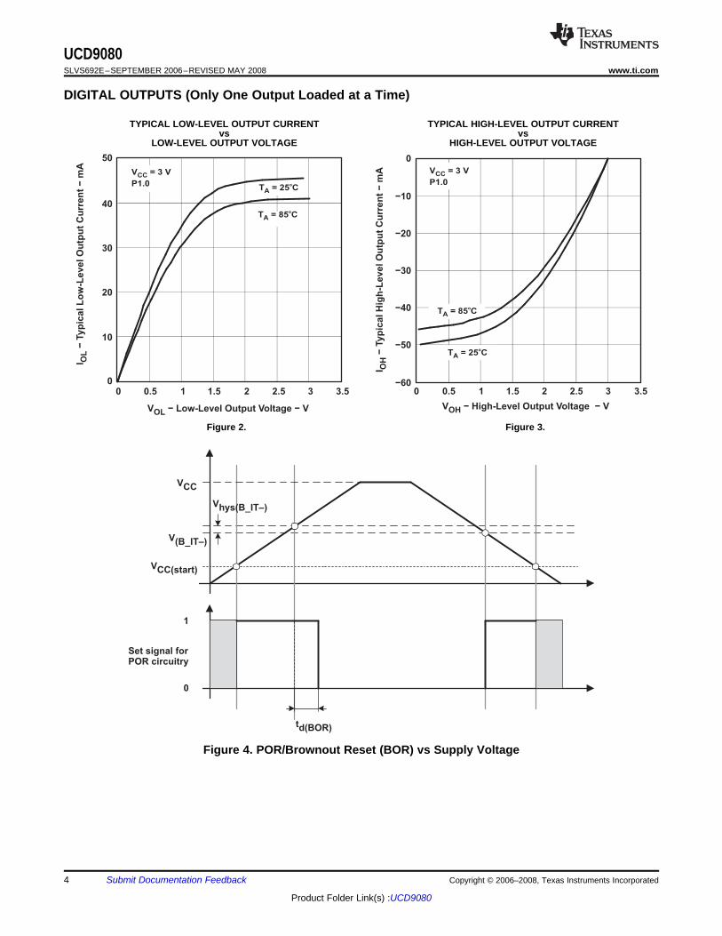
DIGITAL OUTPUTS (Only One Output Loaded at a Time)
V − High-Level Output Voltage − VOH
10−
3
ITy
pic
al
Hig
h-L
ev
el
Ou
tpu
t C
urr
en
tm
AO
H−
−
V = 3 V
P1.0CC
T = 85 CAo
T = 25 CAo
0 0.5 1 1.5 2 3.52.5
−30
0
−50
−20
−60
−40
V − Low-Level Output Voltage − VOL
10
3
ITyp
ical L
ow
-Level O
utp
ut
Cu
rren
tm
AO
L−
−
V = 3 V
P1.0CC
T = 85 CAo
T = 25 CAo
0 0.5 1 1.5 2 3.52.5
30
0
50
20
40
0
1
VCC
V(B_IT–)
Vhys(B_IT–)
VCC(start)
td(BOR)
Set signal forPOR circuitry
UCD9080SLVS692E–SEPTEMBER 2006–REVISED MAY 2008................................................................................................................................................... www.ti.com
TYPICAL LOW-LEVEL OUTPUT CURRENT TYPICAL HIGH-LEVEL OUTPUT CURRENTvs vs
LOW-LEVEL OUTPUT VOLTAGE HIGH-LEVEL OUTPUT VOLTAGE
Figure 2. Figure 3.
Figure 4. POR/Brownout Reset (BOR) vs Supply Voltage
UCD9080www.ti.com................................................................................................................................................... SLVS692E–SEPTEMBER 2006–REVISED MAY 2008
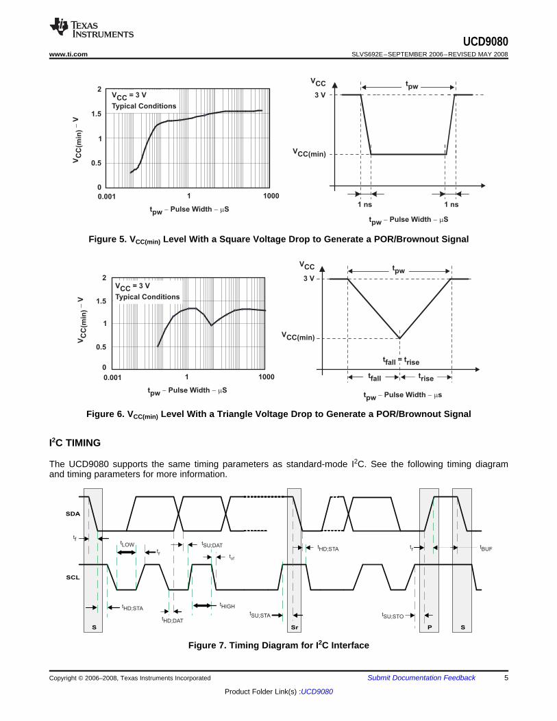
Figure 5. VCC(min) Level With a Square Voltage Drop to Generate a POR/Brownout Signal
Figure 6. VCC(min) Level With a Triangle Voltage Drop to Generate a POR/Brownout Signal
The UCD9080 supports the same timing parameters as standard-mode I2C. See the following timing diagramand timing parameters for more information.
UCD9080SLVS692E–SEPTEMBER 2006–REVISED MAY 2008................................................................................................................................................... www.ti.com
PARAMETER MIN MAX UNITtof Output fall time from VOH to VOL
(1) with a bus capacitance from 10 pF to 400 pF 250 (2) nsCI Capacitance for each pin. 10 pFfSCL SCL clock frequency 10 100 kHztHD;STA Hold time (repeated) START condition. After this period, the first clock pulse is generated. 4 µstHD;DAT Data hold time 0 (3) 3.45 (4) µstLOW LOW period of the SCL clock 4.7 µstHIGH HIGH period of the SCL clock 4 µstSU;STA Set-up time for repeated start condition 4.7 µstSU;DAT Data setup time 250 nstr Rise time of both SDA and SCL signals 1000 nstf Fall time of both SDA and SCL signals 300 nstSU;STO Setup time for STOP condition 4 µstBUF Bus free time between a STOP and START condition 4.7 µsC(b) Capacitive load for each bus line 400 pFVnL Noise margin at the LOW level for each connected device (including hysteresis) 0.1 VDD VVnH Noise margin at the HIGH level for each connected device (including hysteresis) 0.2 VDD V
(1) See the Electrical Characteristics section of this data sheet.(2) The maximum tf for the SDA and SCL bus lines (300 ns) is longer than the specified maximum tof for the output stages (250 ns). This
allows series protection resistors (Rs) to be connected between the SDA/SCL pins and the SDA/SCL bus lines without exceeding themaximum specified tf.
(3) A device must internally provide a hold time of at least 300 ns for the SDA signal to bridge the undefined region of the falling edge ofSCL.
(4) The maximum tHD;DAT must only be met if the device does not stretch the LOW period (tLOW) of the SCL signal.
UCD9080www.ti.com................................................................................................................................................... SLVS692E–SEPTEMBER 2006–REVISED MAY 2008
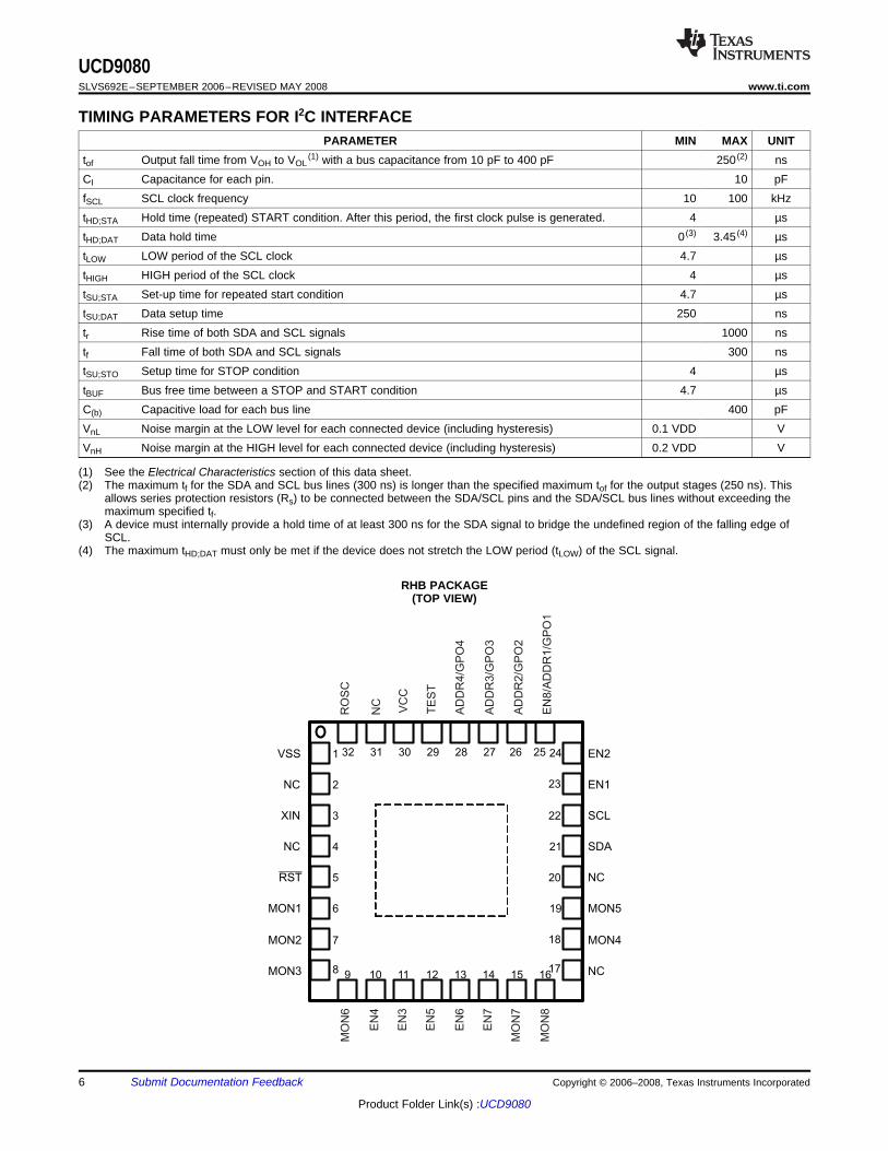
Table 1. TERMINAL FUNCTIONSTERMINAL
I/O DESCRIPTIONNAME NO.ADDR2/GPO2 26 I/O I2C address select 2, general-purpose digital output 2ADDR3/GPO3 27 I/O I2C address select 3, general-purpose digital output 3ADDR4/GPO4 28 I/O I2C address select 4, general-purpose digital output 4EN1 23 I/O Voltage rail 1 enable (digital output)EN2 24 I/O Voltage rail 2 enable (digital output)EN3 11 I/O Voltage rail 3 enable (digital output)EN4 10 I/O Voltage rail 4 enable (digital output)EN5 12 I/O Voltage rail 5 enable (digital output)EN6 13 I/O Voltage rail 6 enable (digital output)EN7 14 I/O Voltage rail 7 enable (digital output)EN8/ADDR1/ 25 I/O Voltage rail 8 enable (digital output), I2C address select 1, general-purpose digital output 1GPO1MON1 6 I Analog input for voltage rail 1MON2 7 I Analog input for voltage rail 2MON3 8 I Analog input for voltage rail 3MON4 18 I Analog input for voltage rail 4MON5 19 I Analog input for voltage rail 5MON6 9 I Analog input for voltage rail 6MON7 15 I Analog input for voltage rail 7MON8 16 I Analog input for voltage rail 8NC 2 Do not connect.
4,17,NC Not connected internally. Connect to VSS.20, 31Internal oscillator frequency adjust. Must use 100-kΩ pullup to VCC for minimum drift and maximumROSC 32 frequency when sampling voltage rails.
RST 5 I Reset inputSCL 22 I/O I2C clock. A pullup rwesistor to 3.3 V is required.SDA 21 I/O I2C data (bidirectional). A pullup resistor to 3.3 V is required.TEST 29 I Connect to VSSVCC 30 Supply voltageVSS 1 Ground referenceXIN 3 Connect to VCC
UCD9080SLVS692E–SEPTEMBER 2006–REVISED MAY 2008................................................................................................................................................... www.ti.com
UCD9080www.ti.com................................................................................................................................................... SLVS692E–SEPTEMBER 2006–REVISED MAY 2008
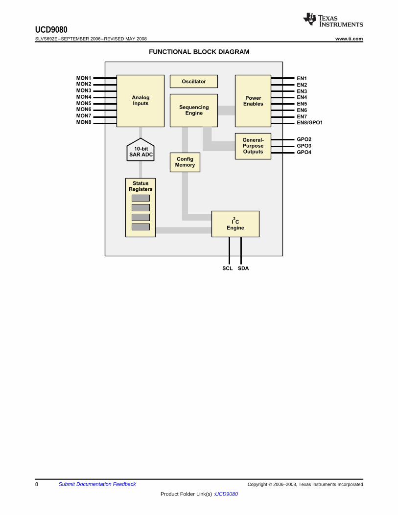
The UCD9080 can be configured to sequence the power rails using the enable signals or the general-purposeoutputs in one of three ways.
The first way is to specify a delay time after a UCD9080 RESET. The enable/GPO is asserted after theUCD9080 RESET plus a specified delay.
The second way is to specify a delay time after another (parent) rail has achieved regulation (that is, VRAIL iswithin the specified under- and overvoltage settings). The enable/GPO is asserted after the (parent) rail is inregulation plus specified delay.
The third way is to specify a (parent) rail voltage. The enable/GPO is asserted after the (parent) rail voltage isgreater than or equal to the specified voltage.
Of course, a rail does not have to be sequenced, as in the case of a backplane voltage that is not under thecontrol of the UCD9080, but is being monitored.
The UCD9080 can sequence up to eight power supplies using the ENx (EN1 to EN8) signals. These signals canbe configured as active-high or active-low, supporting power supplies with either polarity.
EN8 can also be configured as a GPO (GPO1). EN8/ADDR1/GPO1 is also used for I2C address selection(ADDR1).
The UCD9080 can control up to four general-purpose digital outputs using the same sequencing mechanisms asdescribed in the Power-Supply Enables section. These general-purpose outputs (referred to as GPO1–GPO4)can be used for digital signals such as RESET or status. Note that these signals are multiplexed with otherfunctions (primarily I2C address selection). See the Terminal Functions table to ensure that these signals areused properly by the application. Also note that the GPO1 signal is multiplexed with EN8, so both of these cannotbe used at the same time.
During the UCD9080 RESET interval, all ENx and GPOx pins become Schmitt-trigger Inputs. A UCD9080RESET occurs under the following conditions:• External RST pin is driven low.• Power is applied to the device (power-on reset) or power is cycled.• A sequence event occurs as a result of a configured rail-alarm event.• The RESTART register is written with a value of 0 over the I2C bus.
All ENx and GPOx pins must be externally terminated to one of the following Schmitt-trigger input-logic states forproper sequencer operation.• EN or GPO pin configured for ACTIVE-LOW polarity: the external resistor network must default the
corresponding EN or GPO pin to a voltage greater than or equal to 1.9 V (VIT+, MAX, positive-going inputthreshold voltage) during device reset.
• EN or GPO pin configured for ACTIVE-HIGH polarity: the external resistor network must default thecorresponding EN or GPO pin to a voltage less than or equal to 0.9 V (VIT–, MIN, negative-going inputthreshold voltage) during device reset.
NOTE:
The external resistor networks should not derive their voltage from a sequencedpower supply, as this may cause the voltage level presented to the ENx or GPOx pinto be at the wrong level during device reset. It is best to use the UCD9080 VCCsupply for the external resistor networks.
UCD9080SLVS692E–SEPTEMBER 2006–REVISED MAY 2008................................................................................................................................................... www.ti.com
The user must consider GPO polarity usage when programming the UCD9080 I2C address using the externalGPOx (ADDRx) resistor networks. Acceptable ADDRx bit voltage levels are set according to Schmitt-trigger inputspecifications. The following GPOx/ADDRx combinations are acceptable:• GPOx = Active-low polarity: Corresponding ADDRx bit set to Schmitt-trigger input logic level = 1• GPOx = Active-high polarity: Corresponding ADDRx bit set to Schmitt-trigger input logic level = 0
The UCD9080 has a voltage reference that is selectable via the I2C interface and parameter configurationsection. The voltage reference can either be an internally generated 2.5-V reference or an external 3.3-Vreference. If the external voltage reference is selected, then the 3.3-V reference is from the VCC supply to theUCD9080.
Depending on the voltage reference that is being used, the accuracy of reading voltages is affected. The internalreference is not as accurate as the external reference and affects the accuracy of the sampled voltages of themonitored rails. See the Electrical Characteristics for information on voltage reading accuracy for use with eachof the references.
The Configuring the UCD9080 section details how to select the internal or external voltage reference.
The UCD9080 can monitor eight voltage rails through the MONx terminals of the device (MON1–MON8). TheUCD9080 samples these eight input channels using either the internal 2.5-V reference or VCC (3.3 V) as avoltage reference to convert the voltage to digital values. The eight digitally monitored voltage values areaccessible via the I2C interface.
When monitoring a voltage rail that has a nominal voltage larger than 2.5 V (internal reference) or 3.3 V (externalreference), a resistor divider network is typically used. The design must ensure that the source impedance of thatresistor network is not too high, because it causes the UCD9080 analog-to-digital converter (ADC) to take longerto perform the sample-and-hold conversion. The extended conversion time causes the frequency of the samplingof voltage rails to slow below 20 kHz.
Using a higher-valued resistor network lowers the overall power dissipation of the solution, which is desirable. Inorder to keep the source impedance low, a buffer circuit is typically used. The UCD9080 analog inputs requirethat a source impedance of less than 20 kΩ be used in order to maintain the high sampling rate of the voltages.
The UCD9080 allows specification of overvoltage threshold, undervoltage threshold, and out-of-regulation orglitch duration for each monitored rail.
Each voltage rail can also be marked so that it is not monitored, in which case all checks and alarm conditionsare disabled.
Rail shutdown is the act of setting the ENx pin associated with that rail to a state which disables the powersupply output. Each UCD9080 rail can be configured to shut down based on a monitored alarm event (sustainedovervoltage, sustained undervoltage, or rail did not start) and in a configurable manner.
The options for rail shutdown are as follows:• Ignore• Log only• Sequence• Retry 1 time• Retry 0 times
If the system does not care whether a monitored rail enters a sustained error condition, the UCD9080 can beconfigured to either ignore or log the error event and take no subsequent action.
UCD9080www.ti.com................................................................................................................................................... SLVS692E–SEPTEMBER 2006–REVISED MAY 2008
The UCD9080 can also be configured to sequence the entire system in response to a sustained error condition.When the UCD9080 monitors an alarm event on the configured rail, UCD9080 RESET occurs (all ENx andGPOx outputs go to the high-impedance state for ~4–5 ms). Next, a sequence of all configured enables andGPOs occurs, as defined by the current sequencer configuration. Note that for this configuration, a shutdownaccording to the values in the UnsequenceTime register does not occur prior to UCD9080 RESET.
The UCD9080 can also be configured to attempt to restart a rail once in response to a sustained error condition.When the UCD9080 monitors an alarm event on a configured rail, the rail is momentarily disabled and thenre-enabled. The rail remains enabled according to the RampTime register setting (time), and if the rail does notproperly achieve regulation, the system (rail and dependent rails) is shut down as defined by the currentsequencer configuration (UnsequenceTime register).
The last option that the UCD9080 supports is to shut down (if specified as a dependency) and disable (Retry 0times) a configured rail in response to a sustained error condition. When the UCD9080 monitors an alarm eventon the configured rail, the system (dependent rails and GPOs) is shut down as defined by the current sequencerconfiguration (UnsequenceTime register). Only rails and GPOs marked as dependencies of the configured railare shut down. If there are no rails or GPO dependencies marked, the configured rail is just disabled in responseto the sustained error condition.
Each UCD9080 ENx and GPOx output can be marked to sequence after shutdown (as defined by the currentsequencer configuration) if specified as a dependency in the DependencyMasks register. For example, if rail 1 isconfigured to sequence after shutdown (RESEQ bit set), and rail 2 has rail 1 set in its dependency mask, thenif/when rail 2 is shut down, rail 1 shuts down and the system resequences.
The brownout circuit is implemented to provide the proper internal reset signal to the device during power on andpower off.
The UCD9080 power-supply sequencer has a 100-kHz, slave-mode I2C interface for communication with an I2Cmaster. The I2C master uses this interface to configure and monitor the UCD9080.
The UCD9080 supports 7-bit I2C addressing. The UCD9080 selects an I2C address by sampling the logic level ofthe four digital inputs to the device (ADDR1–ADDR4) during the UCD9080 RESET interval. When the UCD9080is released from RESET, the ADDRx logic levels are latched and the I2C address is assigned as shown inFigure 8.
External pullup/pulldown resistors are required to configure the I2C address; the UCD9080 does not have internalbias resistors. Note that the 7-bit I2C address refers to the address bits only, not the read/write (8th) bit in the firstbyte of the I2C protocol. The base I2C address is 0x60 and the I2C general-call address (0x00) is not supported.
After the initialization process of the UCD9080 is complete, these four pins can be used as general-purposeoutputs (GPOs). They can be programmed and sequenced as described in the Configuring the UDC9080section. GPO polarity must consider the external I2C address resistors as described in the ExternalConsiderations for EN and GPO Pins section.
The UCD9080 can be configured and monitored via I2C memory-mapped registers. Registers that areconfigurable (can be written) via an I2C write operation are implemented using an I2C unidirectional data transfer,from the master to slave, with a stop bit between transactions.
UCD9080SLVS692E–SEPTEMBER 2006–REVISED MAY 2008................................................................................................................................................... www.ti.com
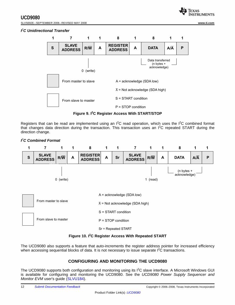
I2C Unidirectional Transfer
Figure 9. I2C Register Access With START/STOP
Registers that can be read are implemented using an I2C read operation, which uses the I2C combined formatthat changes data direction during the transaction. This transaction uses an I2C repeated START during thedirection change.
I2C Combined Format
Figure 10. I2C Register Access With Repeated START
The UCD9080 also supports a feature that auto-increments the register address pointer for increased efficiencywhen accessing sequential blocks of data. It is not necessary to issue separate I2C transactions.
The UCD9080 supports both configuration and monitoring using its I2C slave interface. A Microsoft Windows GUIis available for configuring and monitoring the UCD9080. See the UCD9080 Power Supply Sequencer andMonitor EVM user's guide (SLVU184).
UCD9080www.ti.com................................................................................................................................................... SLVS692E–SEPTEMBER 2006–REVISED MAY 2008
For monitoring the sequencer, an I2C memory map allows an I2C host to perform memory-mapped reads (and insome cases writes) to obtain status information from the UCD9080. For instance, all rails can report their voltagethrough the I2C memory map. For information on which parameters are available via the I2C memory map, seethe Monitoring the UCD9080 section.
To change configuration parameters of the sequencer, a different mechanism is used. The entire set ofconfiguration parameters must be written to the device at one time as one large transaction over the I2C interfaceto ensure that the configuration of the device is consistent at any given time. The process for configuring theUCD9080 is described in the Configuring the UDC9080 section.
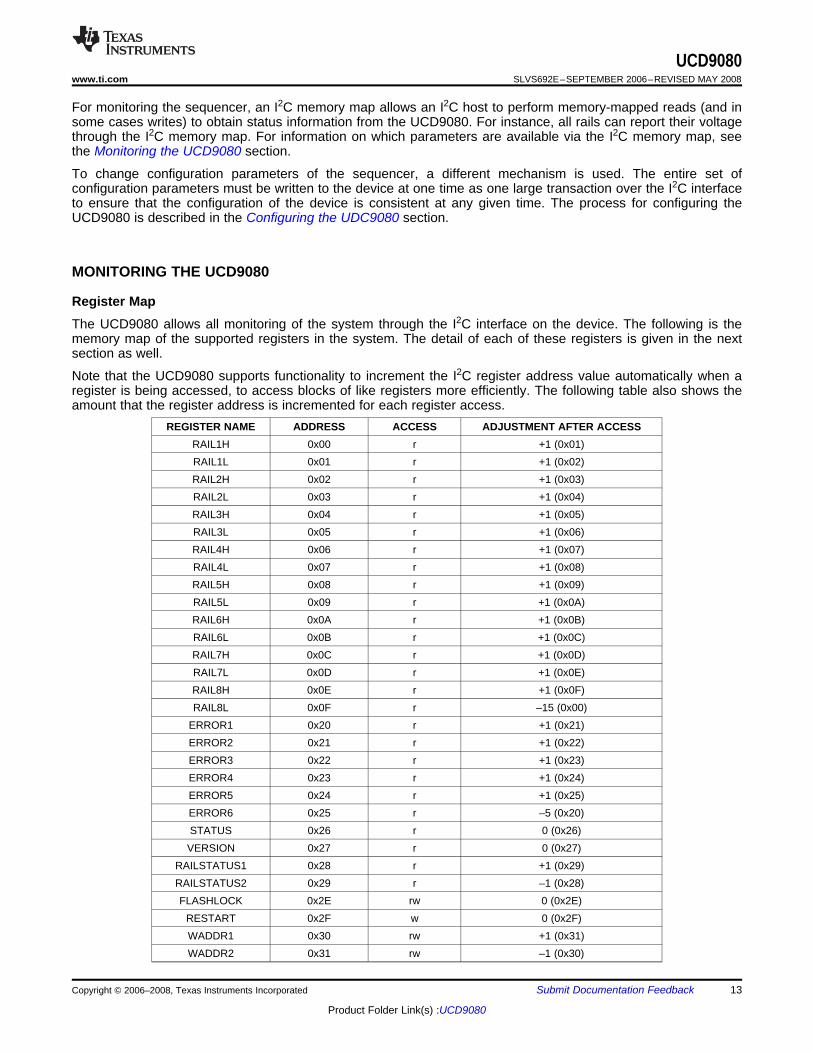
The UCD9080 allows all monitoring of the system through the I2C interface on the device. The following is thememory map of the supported registers in the system. The detail of each of these registers is given in the nextsection as well.
Note that the UCD9080 supports functionality to increment the I2C register address value automatically when aregister is being accessed, to access blocks of like registers more efficiently. The following table also shows theamount that the register address is incremented for each register access.
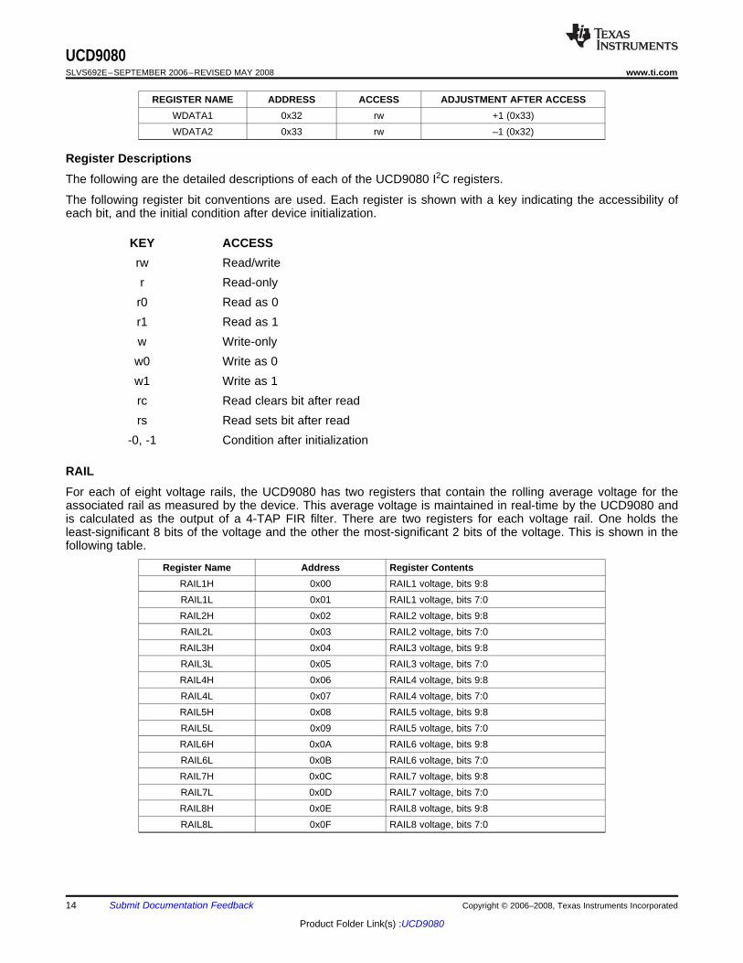
REGISTER NAME ADDRESS ACCESS ADJUSTMENT AFTER ACCESSRAIL1H 0x00 r +1 (0x01)RAIL1L 0x01 r +1 (0x02)RAIL2H 0x02 r +1 (0x03)RAIL2L 0x03 r +1 (0x04)RAIL3H 0x04 r +1 (0x05)RAIL3L 0x05 r +1 (0x06)RAIL4H 0x06 r +1 (0x07)RAIL4L 0x07 r +1 (0x08)RAIL5H 0x08 r +1 (0x09)RAIL5L 0x09 r +1 (0x0A)RAIL6H 0x0A r +1 (0x0B)RAIL6L 0x0B r +1 (0x0C)RAIL7H 0x0C r +1 (0x0D)RAIL7L 0x0D r +1 (0x0E)RAIL8H 0x0E r +1 (0x0F)RAIL8L 0x0F r –15 (0x00)
ERROR1 0x20 r +1 (0x21)ERROR2 0x21 r +1 (0x22)ERROR3 0x22 r +1 (0x23)ERROR4 0x23 r +1 (0x24)ERROR5 0x24 r +1 (0x25)ERROR6 0x25 r –5 (0x20)STATUS 0x26 r 0 (0x26)VERSION 0x27 r 0 (0x27)
RAILSTATUS1 0x28 r +1 (0x29)RAILSTATUS2 0x29 r –1 (0x28)FLASHLOCK 0x2E rw 0 (0x2E)
UCD9080SLVS692E–SEPTEMBER 2006–REVISED MAY 2008................................................................................................................................................... www.ti.com
REGISTER NAME ADDRESS ACCESS ADJUSTMENT AFTER ACCESSWDATA1 0x32 rw +1 (0x33)WDATA2 0x33 rw –1 (0x32)
The following are the detailed descriptions of each of the UCD9080 I2C registers.
The following register bit conventions are used. Each register is shown with a key indicating the accessibility ofeach bit, and the initial condition after device initialization.
KEY ACCESSrw Read/writer Read-only
r0 Read as 0r1 Read as 1w Write-onlyw0 Write as 0w1 Write as 1rc Read clears bit after readrs Read sets bit after read
-0, -1 Condition after initialization
For each of eight voltage rails, the UCD9080 has two registers that contain the rolling average voltage for theassociated rail as measured by the device. This average voltage is maintained in real-time by the UCD9080 andis calculated as the output of a 4-TAP FIR filter. There are two registers for each voltage rail. One holds theleast-significant 8 bits of the voltage and the other the most-significant 2 bits of the voltage. This is shown in thefollowing table.
UCD9080www.ti.com................................................................................................................................................... SLVS692E–SEPTEMBER 2006–REVISED MAY 2008
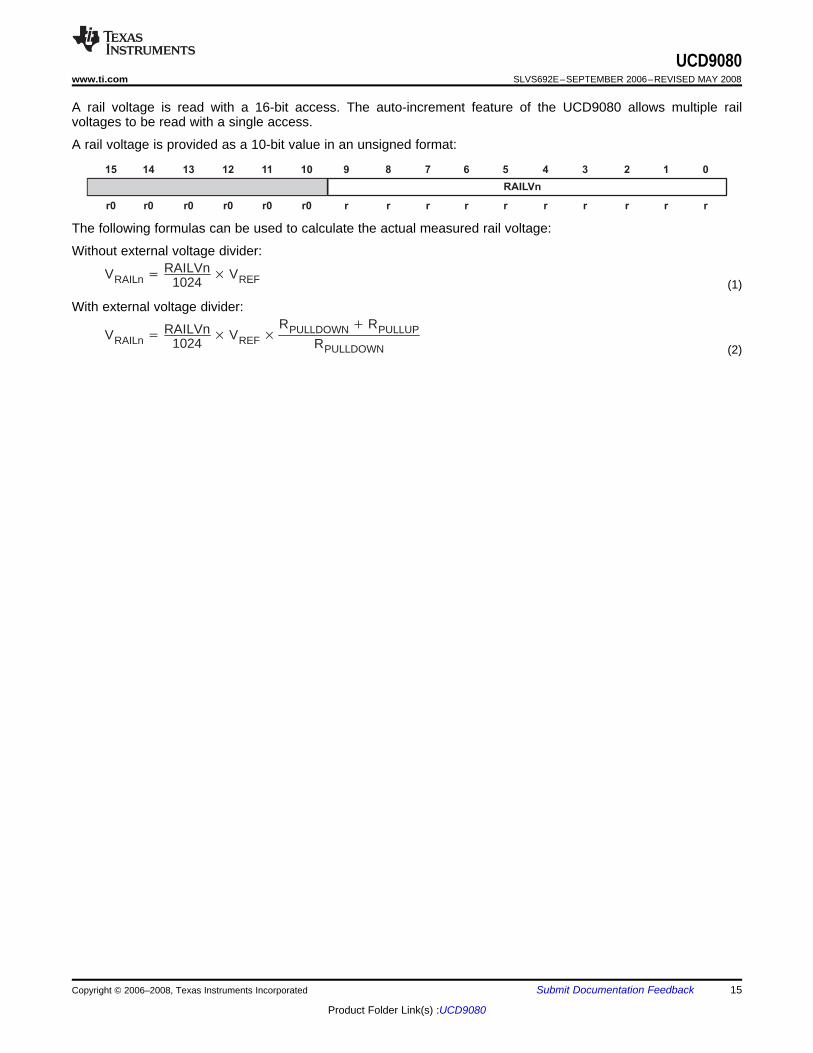
A rail voltage is read with a 16-bit access. The auto-increment feature of the UCD9080 allows multiple railvoltages to be read with a single access.
A rail voltage is provided as a 10-bit value in an unsigned format:
The following formulas can be used to calculate the actual measured rail voltage:
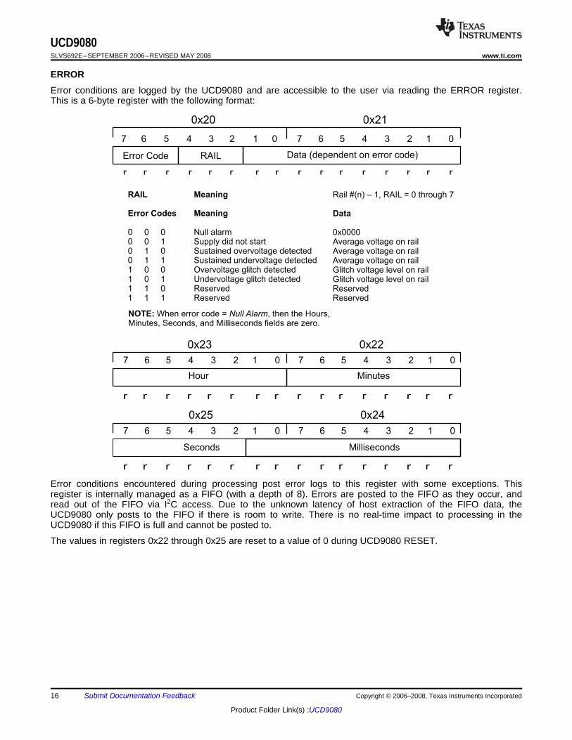
NOTE: When error code = , then the Hours,Minutes, Seconds, and Milliseconds fields are zero.
Null Alarm
Rail #(n) – 1, RAIL = 0 through 7
Average voltage on railAverage voltage on rail
litch voltage level on railGlitch voltage level on rail
Data
0x0000Average voltage on rail
G
ReservedReserved
Hour
Seconds
Minutes
Milliseconds
6 5 4 27 1 03
6 5 4 27 1 036 5 4 27 1 03
UCD9080SLVS692E–SEPTEMBER 2006–REVISED MAY 2008................................................................................................................................................... www.ti.com
Error conditions are logged by the UCD9080 and are accessible to the user via reading the ERROR register.This is a 6-byte register with the following format:
Error conditions encountered during processing post error logs to this register with some exceptions. Thisregister is internally managed as a FIFO (with a depth of 8). Errors are posted to the FIFO as they occur, andread out of the FIFO via I2C access. Due to the unknown latency of host extraction of the FIFO data, theUCD9080 only posts to the FIFO if there is room to write. There is no real-time impact to processing in theUCD9080 if this FIFO is full and cannot be posted to.
The values in registers 0x22 through 0x25 are reset to a value of 0 during UCD9080 RESET.
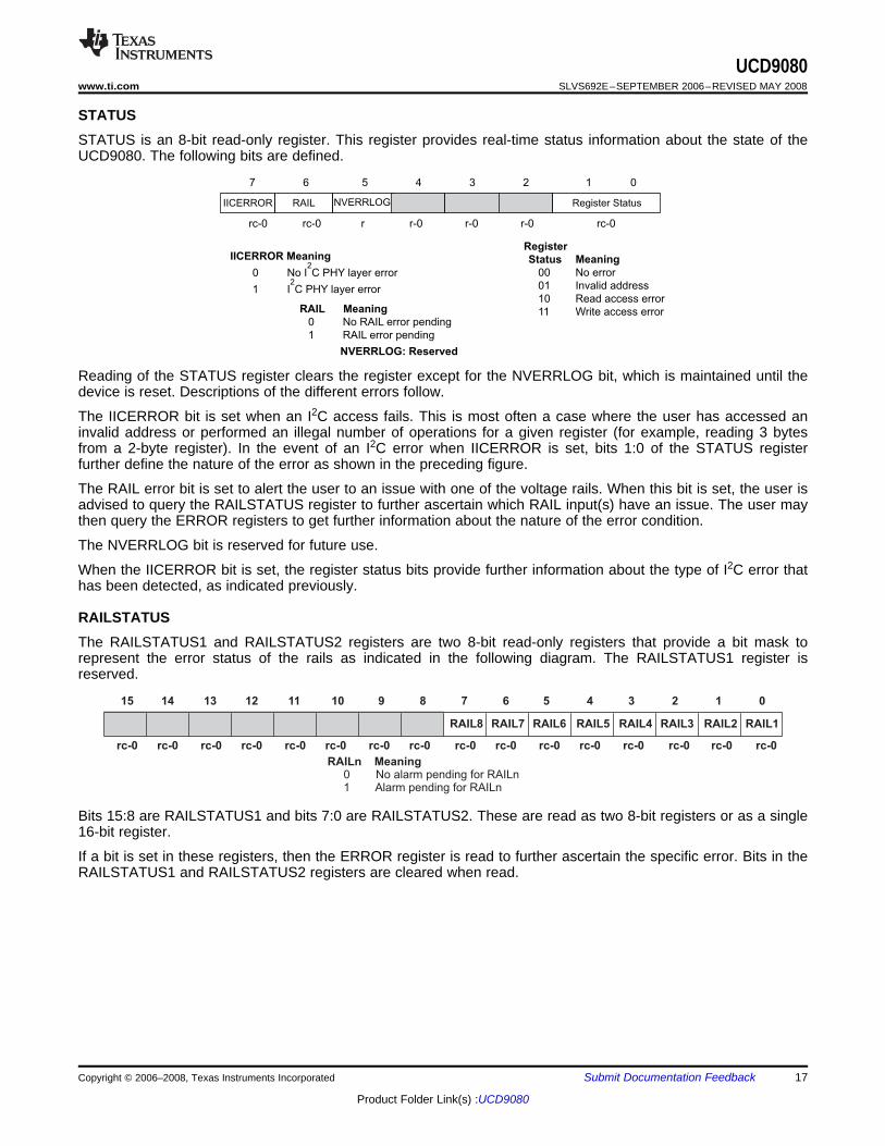
RAILn Meaning0 No alarm pending for R n1 Alarm pending for RAILn
AIL
UCD9080www.ti.com................................................................................................................................................... SLVS692E–SEPTEMBER 2006–REVISED MAY 2008
STATUS is an 8-bit read-only register. This register provides real-time status information about the state of theUCD9080. The following bits are defined.
Reading of the STATUS register clears the register except for the NVERRLOG bit, which is maintained until thedevice is reset. Descriptions of the different errors follow.
The IICERROR bit is set when an I2C access fails. This is most often a case where the user has accessed aninvalid address or performed an illegal number of operations for a given register (for example, reading 3 bytesfrom a 2-byte register). In the event of an I2C error when IICERROR is set, bits 1:0 of the STATUS registerfurther define the nature of the error as shown in the preceding figure.
The RAIL error bit is set to alert the user to an issue with one of the voltage rails. When this bit is set, the user isadvised to query the RAILSTATUS register to further ascertain which RAIL input(s) have an issue. The user maythen query the ERROR registers to get further information about the nature of the error condition.
The NVERRLOG bit is reserved for future use.
When the IICERROR bit is set, the register status bits provide further information about the type of I2C error thathas been detected, as indicated previously.
The RAILSTATUS1 and RAILSTATUS2 registers are two 8-bit read-only registers that provide a bit mask torepresent the error status of the rails as indicated in the following diagram. The RAILSTATUS1 register isreserved.
Bits 15:8 are RAILSTATUS1 and bits 7:0 are RAILSTATUS2. These are read as two 8-bit registers or as a single16-bit register.
If a bit is set in these registers, then the ERROR register is read to further ascertain the specific error. Bits in theRAILSTATUS1 and RAILSTATUS2 registers are cleared when read.
UCD9080SLVS692E–SEPTEMBER 2006–REVISED MAY 2008................................................................................................................................................... www.ti.com
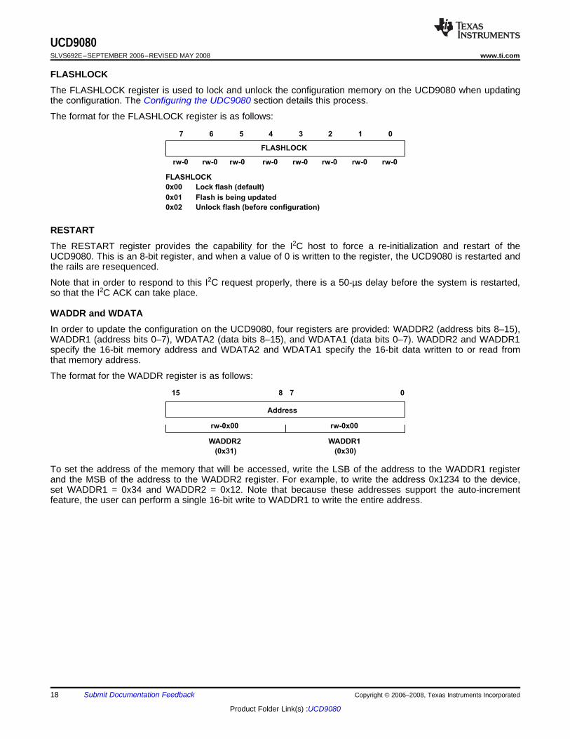
The FLASHLOCK register is used to lock and unlock the configuration memory on the UCD9080 when updatingthe configuration. The Configuring the UDC9080 section details this process.
The format for the FLASHLOCK register is as follows:
The RESTART register provides the capability for the I2C host to force a re-initialization and restart of theUCD9080. This is an 8-bit register, and when a value of 0 is written to the register, the UCD9080 is restarted andthe rails are resequenced.
Note that in order to respond to this I2C request properly, there is a 50-µs delay before the system is restarted,so that the I2C ACK can take place.
In order to update the configuration on the UCD9080, four registers are provided: WADDR2 (address bits 8–15),WADDR1 (address bits 0–7), WDATA2 (data bits 8–15), and WDATA1 (data bits 0–7). WADDR2 and WADDR1specify the 16-bit memory address and WDATA2 and WDATA1 specify the 16-bit data written to or read fromthat memory address.
The format for the WADDR register is as follows:
To set the address of the memory that will be accessed, write the LSB of the address to the WADDR1 registerand the MSB of the address to the WADDR2 register. For example, to write the address 0x1234 to the device,set WADDR1 = 0x34 and WADDR2 = 0x12. Note that because these addresses support the auto-incrementfeature, the user can perform a single 16-bit write to WADDR1 to write the entire address.
Repeat as necessary with WADDR updatedto write 512 bytes
UCD9080www.ti.com................................................................................................................................................... SLVS692E–SEPTEMBER 2006–REVISED MAY 2008
The format for the WDATA register is as follows:
To set the value of the data that will be written, write the LSB of the data to the WDATA1 register and the MSB ofthe data to the WDATA2 register. For example, to write the data 0xBEEF to the device, set WDATA1 = 0xEF andWDATA2 = 0xBE. Note that because these addresses support the auto-increment feature, the user can performa single 16-bit write to WDATA1 to write the entire data. To read the value of the data at the specified address,read the LSB from WDATA1 and the MSB from WDATA2.
These registers are used for updating the UCD9080 configuration as explained in the Configuring the UDC9080section.
The UCD9080 has many different configurable parameters, such as sequencing policies, shutdown policies anddependency masks. The UCD9080 can configure all of its parameters via the I2C interface while the device isoperational. Sequencing, shutdown, and rail monitoring are not performed during device configuration time.
NOTE:
During runtime, if the UCD9080 is configured, there is a delay in voltage monitoringwhile the new configuration parameters are applied to the device.
To configure the UCD9080, a large block of configuration information is sent to the device via the I2C interface.This block is 512 bytes and contains all the configuration information that the device requires for any function ofthe UCD9080.
This 512-byte block of configuration information is sent to the device in multiple segments. The segment size canrange from 2 to 32 bytes at one time, and must be a power of 2 bytes. That is, a master can send 256 2-bytesegments or 32 16-byte segments, and so on. All the segments must be sent back-to-back in the propersequence, and this operation must be completed by sending the last segment so that the last byte of the512-byte block is written. If this is not done, the UCD9080 is in an unknown state and does not function asdesigned.
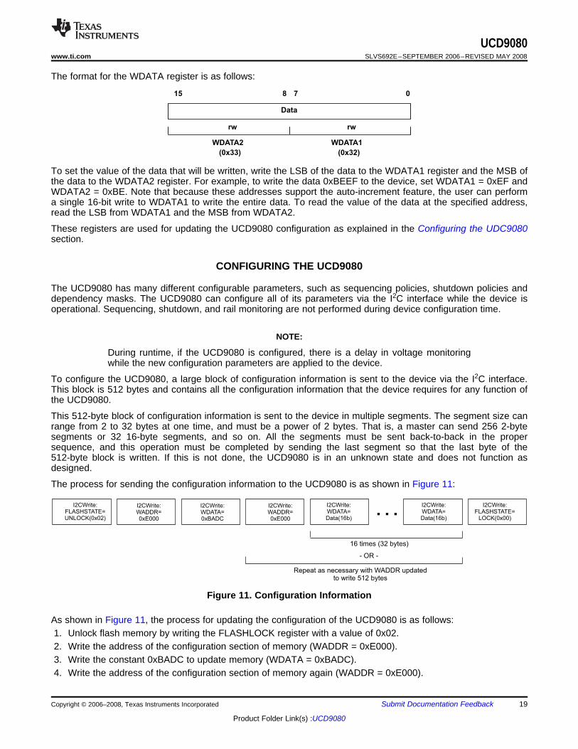
The process for sending the configuration information to the UCD9080 is as shown in Figure 11:
Figure 11. Configuration Information
As shown in Figure 11, the process for updating the configuration of the UCD9080 is as follows:1. Unlock flash memory by writing the FLASHLOCK register with a value of 0x02.2. Write the address of the configuration section of memory (WADDR = 0xE000).3. Write the constant 0xBADC to update memory (WDATA = 0xBADC).4. Write the address of the configuration section of memory again (WADDR = 0xE000).
UCD9080SLVS692E–SEPTEMBER 2006–REVISED MAY 2008................................................................................................................................................... www.ti.com
5. Write the data (WDATA = <varies>). Repeat steps 4 and 5 as necessary, depending on the data segmentsize used, to write 512 bytes. Increment the address as necessary.
6. Lock flash memory after the last byte of the last segment is written by writing the FLASHLOCK register witha value of 0x00.
At the conclusion of this process, the configuration of the UCD9080 is updated with the configuration changes, asrepresented by the values from the data segments. The UCD9080 can then be reset by writing the RESTARTregister with a value of 0. The new sequencer configuration then starts.
The memory map for the 512-byte configuration segment is defined in the Configuration Parameters Detailsection.
User data (128 bytes) can be stored in the UCD9080 user-data area at memory location 0x1080 to 0x10FF.Access to the user-data area occurs by following the procedure outlined in the Configuring the UCD9080 section.
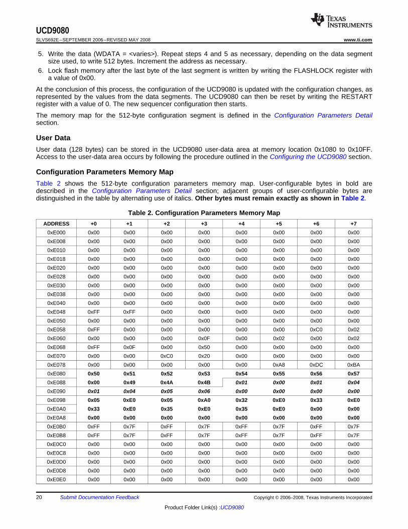
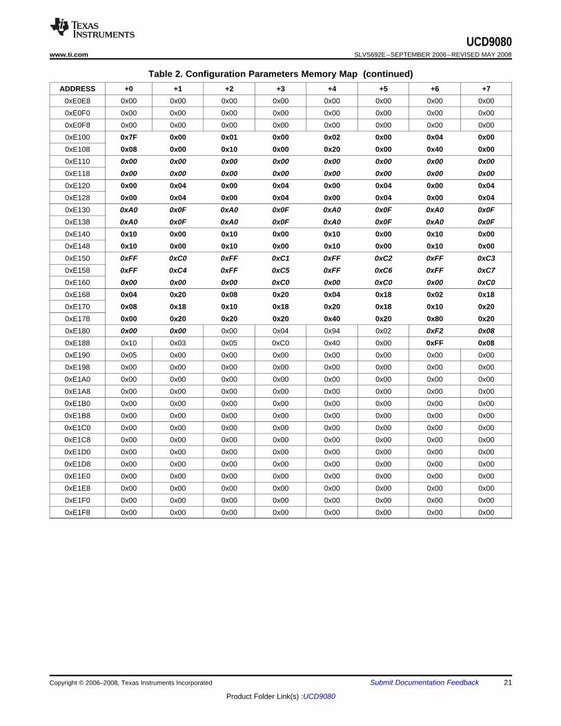
Table 2 shows the 512-byte configuration parameters memory map. User-configurable bytes in bold aredescribed in the Configuration Parameters Detail section; adjacent groups of user-configurable bytes aredistinguished in the table by alternating use of italics. Other bytes must remain exactly as shown in Table 2.
UCD9080www.ti.com................................................................................................................................................... SLVS692E–SEPTEMBER 2006–REVISED MAY 2008
Do not monitor rail status (for event sequencing of GPOs)
Monitor rail status
ENABLE
00
01
10
11
Meaning
Sequence is disabled
Sequence is triggered after delay after sequence event
Sequence is triggered after parent rail achieves voltage level
Sequence is triggered after delay after parent rail achieves voltage regulation
UCD9080SLVS692E–SEPTEMBER 2006–REVISED MAY 2008................................................................................................................................................... www.ti.com
The following sections detail the format and meaning of the configuration parameters from the ConfigurationParameters Memory Map, Table 2.
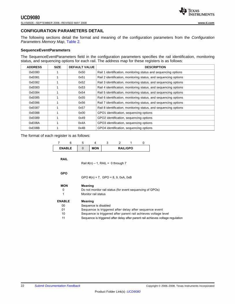
The SequenceEventParameters field in the configuration parameters specifies the rail identification, monitoringstatus, and sequencing options for each rail. The address map for these registers is as follows:
Sequence is dependent on RAIL1 achieving the specified event.Sequence is dependent on RAIL2 achieving the specified event.Sequence is dependent on RAIL3 achieving the specified event.Sequence is dependent on RAIL4 achieving the specified event.Sequence is dependent on RAIL5 achieving the specified event.Sequence is dependent on RAIL6 achieving the specified event.Sequence is dependent on RAIL7 achieving the specified event.Sequence is dependent on RAIL8 achieving the specified event.
Sequence after shutdown.
0x00000x00010x00100x00110x01000x01010x01100x0111
00 0
Do not sequence after shutdown.
UCD9080www.ti.com................................................................................................................................................... SLVS692E–SEPTEMBER 2006–REVISED MAY 2008
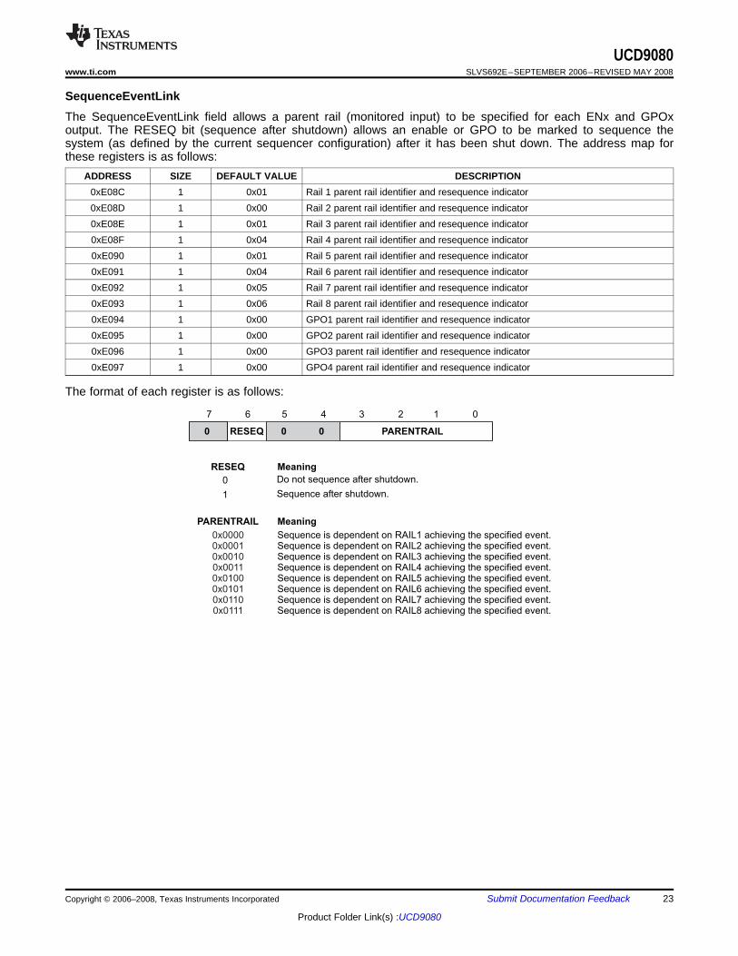
The SequenceEventLink field allows a parent rail (monitored input) to be specified for each ENx and GPOxoutput. The RESEQ bit (sequence after shutdown) allows an enable or GPO to be marked to sequence thesystem (as defined by the current sequencer configuration) after it has been shut down. The address map forthese registers is as follows:
ADDRESS SIZE DEFAULT VALUE DESCRIPTION0xE08C 1 0x01 Rail 1 parent rail identifier and resequence indicator0xE08D 1 0x00 Rail 2 parent rail identifier and resequence indicator0xE08E 1 0x01 Rail 3 parent rail identifier and resequence indicator0xE08F 1 0x04 Rail 4 parent rail identifier and resequence indicator0xE090 1 0x01 Rail 5 parent rail identifier and resequence indicator0xE091 1 0x04 Rail 6 parent rail identifier and resequence indicator0xE092 1 0x05 Rail 7 parent rail identifier and resequence indicator0xE093 1 0x06 Rail 8 parent rail identifier and resequence indicator0xE094 1 0x00 GPO1 parent rail identifier and resequence indicator0xE095 1 0x00 GPO2 parent rail identifier and resequence indicator0xE096 1 0x00 GPO3 parent rail identifier and resequence indicator0xE097 1 0x00 GPO4 parent rail identifier and resequence indicator
Delay (in units of ms)Voltage (in units of Vref/1024 volts)Delay ( ms)in units of
0
UCD9080SLVS692E–SEPTEMBER 2006–REVISED MAY 2008................................................................................................................................................... www.ti.com
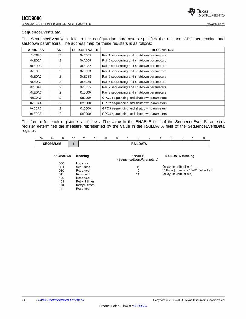
The SequenceEventData field in the configuration parameters specifies the rail and GPO sequencing andshutdown parameters. The address map for these registers is as follows:
ADDRESS SIZE DEFAULT VALUE DESCRIPTION0xE098 2 0xE005 Rail 1 sequencing and shutdown parameters0xE09A 2 0xA005 Rail 2 sequencing and shutdown parameters0xE09C 2 0xE032 Rail 3 sequencing and shutdown parameters0xE09E 2 0xE033 Rail 4 sequencing and shutdown parameters0xE0A0 2 0xE033 Rail 5 sequencing and shutdown parameters0xE0A2 2 0xE035 Rail 6 sequencing and shutdown parameters0xE0A4 2 0xE035 Rail 7 sequencing and shutdown parameters0xE0A6 2 0x0000 Rail 8 sequencing and shutdown parameters0xE0A8 2 0x0000 GPO1 sequencing and shutdown parameters0xE0AA 2 0x0000 GPO2 sequencing and shutdown parameters0xE0AC 2 0x0000 GPO3 sequencing and shutdown parameters0xE0AE 2 0x0000 GPO4 sequencing and shutdown parameters
The format for each register is as follows. The value in the ENABLE field of the SequenceEventParametersregister determines the measure represented by the value in the RAILDATA field of the SequenceEventDataregister.
UCD9080www.ti.com................................................................................................................................................... SLVS692E–SEPTEMBER 2006–REVISED MAY 2008
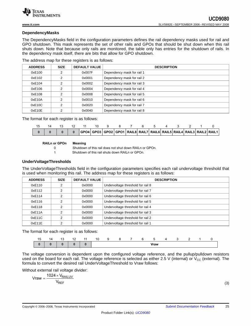
The DependencyMasks field in the configuration parameters defines the rail dependency masks used for rail andGPO shutdown. This mask represents the set of other rails and GPOs that should be shut down when this railshuts down. Note that because only rails are monitored, the table only has entries for the shutdown of rails. Inthe dependency mask itself, there are bits that allow for GPO shutdown.
The address map for these registers is as follows:ADDRESS SIZE DEFAULT VALUE DESCRIPTION
0xE100 2 0x007F Dependency mask for rail 10xE102 2 0x0001 Dependency mask for rail 20xE104 2 0x0002 Dependency mask for rail 30xE106 2 0x0004 Dependency mask for rail 40xE108 2 0x0008 Dependency mask for rail 50xE10A 2 0x0010 Dependency mask for rail 60xE10C 2 0x0020 Dependency mask for rail 70xE10E 2 0x0040 Dependency mask for rail 8
The format for each register is as follows:
The UnderVoltageThresholds field in the configuration parameters specifies each rail undervoltage threshold thatis used when monitoring this rail. The address map for these registers is as follows:
ADDRESS SIZE DEFAULT VALUE DESCRIPTION0xE110 2 0x0000 Undervoltage threshold for rail 80xE112 2 0x0000 Undervoltage threshold for rail 70xE114 2 0x0000 Undervoltage threshold for rail 60xE116 2 0x0000 Undervoltage threshold for rail 50xE118 2 0x0000 Undervoltage threshold for rail 40xE11A 2 0x0000 Undervoltage threshold for rail 30xE11C 2 0x0000 Undervoltage threshold for rail 20xE11E 2 0x0000 Undervoltage threshold for rail 1
The format for each register is as follows:
The voltage conversion is dependent upon the configured voltage reference, and the pullup/pulldown resistorsused on the board for each rail. The voltage reference is selected as either 2.5 V (internal) or VCC (external). Theformula to convert the desired rail UnderVoltageThreshold to Vraw follows:
UCD9080SLVS692E–SEPTEMBER 2006–REVISED MAY 2008................................................................................................................................................... www.ti.com
With external rail voltage divider:
The OverVoltageThreholds field in the configuration parameters specifies each rail overvoltage threshold that isused when monitoring this rail. The address map for these registers is as follows:
ADDRESS SIZE DEFAULT VALUE DESCRIPTION0xE120 2 0x0400 Overvoltage threshold for rail 80xE122 2 0x0400 Overvoltage threshold for rail 70xE124 2 0x0400 Overvoltage threshold for rail 60xE126 2 0x0400 Overvoltage threshold for rail 50xE128 2 0x0400 Overvoltage threshold for rail 40xE12A 2 0x0400 Overvoltage threshold for rail 30xE12C 2 0x0400 Overvoltage threshold for rail 20xE12E 2 0x0400 Overvoltage threshold for rail 1
The format for each register is as follows:
The voltage conversion is dependent upon the configured voltage reference, and the pullup/pulldown resistorsused on the board for each rail. The voltage reference is selected as either 2.5 V (internal) or VCC (external). Theformula to convert the desired rail OverVoltageThreshold to Vraw follows:
Without external rail voltage divider:
With external voltage divider:
The RampTime field in the configuration parameters specifies the maximum amount of time for each rail toachieve regulation. The address map for these registers is as follows:
ADDRESS SIZE DEFAULT VALUE DESCRIPTION0xE130 2 0x0FA0 Maximum voltage ramp time for rail 10xE132 2 0x0FA0 Maximum voltage ramp time for rail 20xE134 2 0x0FA0 Maximum voltage ramp time for rail 30xE136 2 0x0FA0 Maximum voltage ramp time for rail 40xE138 2 0x0FA0 Maximum voltage ramp time for rail 50xE13A 2 0x0FA0 Maximum voltage ramp time for rail 60xE13C 2 0x0FA0 Maximum voltage ramp time for rail 70xE13E 2 0x0FA0 Maximum voltage ramp time for rail 8
OORW = RAILn out-of-regulation glitch width (in units of 1/10 ms).
0 0 00
UnsequenceTime
89101112131415 01234567
USTIME
USTIME = RAILn UnsequenceTime (in units of ms).COPYSEQPARAM = Copy SEQPARAM bit value(bits 15:13) in SequenceEvent Data register
COPYSEQPARAM 0
UCD9080www.ti.com................................................................................................................................................... SLVS692E–SEPTEMBER 2006–REVISED MAY 2008
The OutOfRegulationWidth field in the configuration parameters specifies the maximum amount of time that therail is allowed to be out of regulation before an error is declared (glitch duration). The address map for theseregisters is as follows:
ADDRESS SIZE DEFAULT VALUE DESCRIPTION0xE140 2 0x0010 The out-of-regulation duration permissible without flagging error for rail 10xE142 2 0x0010 The out-of-regulation duration permissible without flagging error for rail 20xE144 2 0x0010 The out-of-regulation duration permissible without flagging error for rail 30xE146 2 0x0010 The out-of-regulation duration permissible without flagging error for rail 40xE148 2 0x0010 The out-of-regulation duration permissible without flagging error for rail 50xE14A 2 0x0010 The out-of-regulation duration permissible without flagging error for rail 60xE14C 2 0x0010 The out-of-regulation duration permissible without flagging error for rail 70xE14E 2 0x0010 The out-of-regulation duration permissible without flagging error for rail 8
The contents of this register are as follows:
The UnsequenceTime field in the configuration parameters specifies the amount of time that each rail shoulddelay before unsequencing. The address map for these registers is as follows:
ADDRESS SIZE DEFAULT VALUE DESCRIPTION0xE150 2 0xC0FF Unsequence delay for rail 10xE152 2 0xC1FF Unsequence delay for rail 20xE154 2 0xC2FF Unsequence delay for rail 30xE156 2 0xC3FF Unsequence delay for rail 40xE158 2 0xC4FF Unsequence delay for rail 50xE15A 2 0xC5FF Unsequence delay for rail 60xE15C 2 0xC6FF Unsequence delay for rail 70xE15E 2 0xC7FF Unsequence delay for rail 80xE160 2 0x0000 Unsequence delay for GPO10xE162 2 0xC000 Unsequence delay for GPO20xE164 2 0xC000 Unsequence delay for GPO30xE166 2 0xC000 Unsequence delay for GPO4
LUTIME = Maximum value USTIME + 255 (in units of ms)
UCD9080SLVS692E–SEPTEMBER 2006–REVISED MAY 2008................................................................................................................................................... www.ti.com
The EnablePolarity field in the configuration parameters specifies whether each power-supply enable or GPO isto be configured active-high or active-low. The address map for these registers is as follows:
ADDRESS SIZE DEFAULT VALUE DESCRIPTION0xE168 2 0x2004 Polarity for rail 1 enable0xE16A 2 0x2008 Polarity for rail 2 enable0xE16C 2 0x1804 Polarity for rail 3 enable0xE16E 2 0x1802 Polarity for rail 4 enable0xE170 2 0x1808 Polarity for rail 5 enable0xE172 2 0x1810 Polarity for rail 6 enable0xE174 2 0x1820 Polarity for rail 7 enable0xE176 2 0x2010 Polarity for rail 8 enable0xE178 2 0x2000 Polarity for GPO10xE17A 2 0x2020 Polarity for GPO20xE17C 2 0x2040 Polarity for GPO30xE17E 2 0x2080 Polarity for GPO4
The contents of this register are as follows:
The ReferenceSelect field in the configuration parameters specifies which voltage reference is used on theUCD9080. The selected reference can be internal (2.5-V), or external via VCC (3.3 V). The register address is0xE186 and contents are as follows:
The default value for this register is 0x08F2, which selects the external reference.
The LastUnusedSeq field in the configuration parameters specifies the amount of time for the last rail to be shutdown without creating an error. The register address is 0xE18E and contents are as follows:
UCD9080www.ti.com................................................................................................................................................... SLVS692E–SEPTEMBER 2006–REVISED MAY 2008
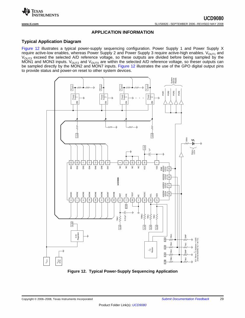
Figure 12 illustrates a typical power-supply sequencing configuration. Power Supply 1 and Power Supply Xrequire active-low enables, whereas Power Supply 2 and Power Supply 3 require active-high enables. VOUT1 andVOUT3 exceed the selected A/D reference voltage, so these outputs are divided before being sampled by theMON1 and MON3 inputs. VOUT2 and VOUTX are within the selected A/D reference voltage, so theser outputs canbe sampled directly by the MON2 and MON7 inputs. Figure 12 illustrates the use of the GPO digital output pinsto provide status and power-on reset to other system devices.
UCD9080SLVS692E–SEPTEMBER 2006–REVISED MAY 2008................................................................................................................................................... www.ti.com
Changes from Revision D (December 2007) to Revision E ........................................................................................... Page
• Deleted ordering information table......................................................................................................................................... 2• Changed NOM and MAX supply current specifications......................................................................................................... 2• Updated Schmitt-trigger input signal list to add the ENx pins (inputs during reset) .............................................................. 2• Removed signal list from high-impedance leakage current specification .............................................................................. 2• Updated the digital output signal list to include the SCL pin (for clock stretching)................................................................ 3• Updated the directionality for the ENx and SCL pins ............................................................................................................ 7• Clarified wording .................................................................................................................................................................... 9• Clarified wording in several sentences and removed note at end of paragraph ................................................................... 9• Moved this section to follow the Power-Supply Enables section. Minor wording change ..................................................... 9• Added new section to describe ENx and GPOx behavior during device reset, and to describe I2C address and
GPOx polarity relationship ..................................................................................................................................................... 9• Clarified wording in sequence paragraph ............................................................................................................................ 10• Clarified wording in several paragraphs .............................................................................................................................. 11• Clarified device time counter reset ...................................................................................................................................... 16• Clarified FLASHLOCK wording............................................................................................................................................ 18• Clarified RESTART wording ................................................................................................................................................ 18• Clarified WDATA/WADDR wording...................................................................................................................................... 18• Clarified wording in several steps ........................................................................................................................................ 19• Changed pin names from NIC to NC for pins 2, 4, 17, 20, 31............................................................................................. 29
Changes from Revision C (January 2007) to Revision D ............................................................................................... Page
• Changed minimum analog supply and positive built-in reference active VCC(min) voltage. Removed minimumsampling voltage, 1.5-V internal reference, and DCO OPERATING PERIOD specifications. .............................................. 3
• Added specification for data hold time, tHD;DAT and notes 3 and 4......................................................................................... 6• Changed pin #2 from "connect to VSS" to "do not connect" ................................................................................................. 7• Removed critica-rail-specification sentence from paragraph 4............................................................................................ 10• Added Ignore option and updated available retry options. Updated descriptions of options .............................................. 10• Added version register and changed WDATA access type from w to rw ........................................................................... 13• Removed reference to flash and non-volatile error log feature in NVERRLOG bit description........................................... 17• Change WDATA access type from w to rw......................................................................................................................... 19• Removed Resetting the Flash Error Logs section ............................................................................................................... 19• Added the UserData section................................................................................................................................................ 20• Updated factory byte values ................................................................................................................................................ 20• Updated factory byte values ................................................................................................................................................ 21• Removed retry 2, retry 3, retry 4, and retry continuously options........................................................................................ 24• Removed SaveRailLog register description......................................................................................................................... 28• Removed pin-2 connection to ground.................................................................................................................................. 29
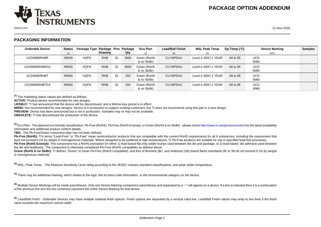
UCD9080RHBR NRND VQFN RHB 32 3000 Green (RoHS& no Sb/Br)
CU NIPDAU Level-2-260C-1 YEAR -40 to 85 UCD9080
UCD9080RHBRG4 NRND VQFN RHB 32 3000 Green (RoHS& no Sb/Br)
CU NIPDAU Level-2-260C-1 YEAR -40 to 85 UCD9080
UCD9080RHBT NRND VQFN RHB 32 250 Green (RoHS& no Sb/Br)
CU NIPDAU Level-2-260C-1 YEAR -40 to 85 UCD9080
UCD9080RHBTG4 NRND VQFN RHB 32 250 Green (RoHS& no Sb/Br)
CU NIPDAU Level-2-260C-1 YEAR -40 to 85 UCD9080
(1) The marketing status values are defined as follows:ACTIVE: Product device recommended for new designs.LIFEBUY: TI has announced that the device will be discontinued, and a lifetime-buy period is in effect.NRND: Not recommended for new designs. Device is in production to support existing customers, but TI does not recommend using this part in a new design.PREVIEW: Device has been announced but is not in production. Samples may or may not be available.OBSOLETE: TI has discontinued the production of the device.
(2) Eco Plan - The planned eco-friendly classification: Pb-Free (RoHS), Pb-Free (RoHS Exempt), or Green (RoHS & no Sb/Br) - please check http://www.ti.com/productcontent for the latest availabilityinformation and additional product content details.TBD: The Pb-Free/Green conversion plan has not been defined.Pb-Free (RoHS): TI's terms "Lead-Free" or "Pb-Free" mean semiconductor products that are compatible with the current RoHS requirements for all 6 substances, including the requirement thatlead not exceed 0.1% by weight in homogeneous materials. Where designed to be soldered at high temperatures, TI Pb-Free products are suitable for use in specified lead-free processes.Pb-Free (RoHS Exempt): This component has a RoHS exemption for either 1) lead-based flip-chip solder bumps used between the die and package, or 2) lead-based die adhesive used betweenthe die and leadframe. The component is otherwise considered Pb-Free (RoHS compatible) as defined above.Green (RoHS & no Sb/Br): TI defines "Green" to mean Pb-Free (RoHS compatible), and free of Bromine (Br) and Antimony (Sb) based flame retardants (Br or Sb do not exceed 0.1% by weightin homogeneous material)
(3) MSL, Peak Temp. - The Moisture Sensitivity Level rating according to the JEDEC industry standard classifications, and peak solder temperature.
(4) There may be additional marking, which relates to the logo, the lot trace code information, or the environmental category on the device.
(5) Multiple Device Markings will be inside parentheses. Only one Device Marking contained in parentheses and separated by a "~" will appear on a device. If a line is indented then it is a continuationof the previous line and the two combined represent the entire Device Marking for that device.
(6) Lead/Ball Finish - Orderable Devices may have multiple material finish options. Finish options are separated by a vertical ruled line. Lead/Ball Finish values may wrap to two lines if the finishvalue exceeds the maximum column width.
Important Information and Disclaimer:The information provided on this page represents TI's knowledge and belief as of the date that it is provided. TI bases its knowledge and belief on informationprovided by third parties, and makes no representation or warranty as to the accuracy of such information. Efforts are underway to better integrate information from third parties. TI has taken andcontinues to take reasonable steps to provide representative and accurate information but may not have conducted destructive testing or chemical analysis on incoming materials and chemicals.TI and TI suppliers consider certain information to be proprietary, and thus CAS numbers and other limited information may not be available for release.
In no event shall TI's liability arising out of such information exceed the total purchase price of the TI part(s) at issue in this document sold by TI to Customer on an annual basis.
Texas Instruments Incorporated and its subsidiaries (TI) reserve the right to make corrections, enhancements, improvements and otherchanges to its semiconductor products and services per JESD46, latest issue, and to discontinue any product or service per JESD48, latestissue. Buyers should obtain the latest relevant information before placing orders and should verify that such information is current andcomplete. All semiconductor products (also referred to herein as “components”) are sold subject to TI’s terms and conditions of salesupplied at the time of order acknowledgment.TI warrants performance of its components to the specifications applicable at the time of sale, in accordance with the warranty in TI’s termsand conditions of sale of semiconductor products. Testing and other quality control techniques are used to the extent TI deems necessaryto support this warranty. Except where mandated by applicable law, testing of all parameters of each component is not necessarilyperformed.TI assumes no liability for applications assistance or the design of Buyers’ products. Buyers are responsible for their products andapplications using TI components. To minimize the risks associated with Buyers’ products and applications, Buyers should provideadequate design and operating safeguards.TI does not warrant or represent that any license, either express or implied, is granted under any patent right, copyright, mask work right, orother intellectual property right relating to any combination, machine, or process in which TI components or services are used. Informationpublished by TI regarding third-party products or services does not constitute a license to use such products or services or a warranty orendorsement thereof. Use of such information may require a license from a third party under the patents or other intellectual property of thethird party, or a license from TI under the patents or other intellectual property of TI.Reproduction of significant portions of TI information in TI data books or data sheets is permissible only if reproduction is without alterationand is accompanied by all associated warranties, conditions, limitations, and notices. TI is not responsible or liable for such altereddocumentation. Information of third parties may be subject to additional restrictions.Resale of TI components or services with statements different from or beyond the parameters stated by TI for that component or servicevoids all express and any implied warranties for the associated TI component or service and is an unfair and deceptive business practice.TI is not responsible or liable for any such statements.Buyer acknowledges and agrees that it is solely responsible for compliance with all legal, regulatory and safety-related requirementsconcerning its products, and any use of TI components in its applications, notwithstanding any applications-related information or supportthat may be provided by TI. Buyer represents and agrees that it has all the necessary expertise to create and implement safeguards whichanticipate dangerous consequences of failures, monitor failures and their consequences, lessen the likelihood of failures that might causeharm and take appropriate remedial actions. Buyer will fully indemnify TI and its representatives against any damages arising out of the useof any TI components in safety-critical applications.In some cases, TI components may be promoted specifically to facilitate safety-related applications. With such components, TI’s goal is tohelp enable customers to design and create their own end-product solutions that meet applicable functional safety standards andrequirements. Nonetheless, such components are subject to these terms.No TI components are authorized for use in FDA Class III (or similar life-critical medical equipment) unless authorized officers of the partieshave executed a special agreement specifically governing such use.Only those TI components which TI has specifically designated as military grade or “enhanced plastic” are designed and intended for use inmilitary/aerospace applications or environments. Buyer acknowledges and agrees that any military or aerospace use of TI componentswhich have not been so designated is solely at the Buyer's risk, and that Buyer is solely responsible for compliance with all legal andregulatory requirements in connection with such use.TI has specifically designated certain components as meeting ISO/TS16949 requirements, mainly for automotive use. In any case of use ofnon-designated products, TI will not be responsible for any failure to meet ISO/TS16949.
Products ApplicationsAudio www.ti.com/audio Automotive and Transportation www.ti.com/automotiveAmplifiers amplifier.ti.com Communications and Telecom www.ti.com/communicationsData Converters dataconverter.ti.com Computers and Peripherals www.ti.com/computersDLP® Products www.dlp.com Consumer Electronics www.ti.com/consumer-appsDSP dsp.ti.com Energy and Lighting www.ti.com/energyClocks and Timers www.ti.com/clocks Industrial www.ti.com/industrialInterface interface.ti.com Medical www.ti.com/medicalLogic logic.ti.com Security www.ti.com/securityPower Mgmt power.ti.com Space, Avionics and Defense www.ti.com/space-avionics-defenseMicrocontrollers microcontroller.ti.com Video and Imaging www.ti.com/videoRFID www.ti-rfid.comOMAP Applications Processors www.ti.com/omap TI E2E Community e2e.ti.comWireless Connectivity www.ti.com/wirelessconnectivity