A 350 mK, 9 T scanning tunneling microscope for the study of superconducting thin films on insulating substrates and single crystals Anand Kamlapure, Garima Saraswat, Somesh Chandra Ganguli, Vivas Bagwe, Pratap Raychaudhuri, and Subash P. Pai Citation: Review of Scientific Instruments 84, 123905 (2013); doi: 10.1063/1.4849616 View online: http://dx.doi.org/10.1063/1.4849616 View Table of Contents: http://scitation.aip.org/content/aip/journal/rsi/84/12?ver=pdfcov Published by the AIP Publishing This article is copyrighted as indicated in the article. Reuse of AIP content is subject to the terms at: http://scitationnew.aip.org/termsconditions. Downloaded to IP: 158.144.59.171 On: Thu, 26 Dec 2013 16:58:12
Transcript
A 350 mK, 9 T scanning tunneling microscope for the study of superconducting thinfilms on insulating substrates and single crystalsAnand Kamlapure, Garima Saraswat, Somesh Chandra Ganguli, Vivas Bagwe, Pratap Raychaudhuri, and
Subash P. Pai Citation: Review of Scientific Instruments 84, 123905 (2013); doi: 10.1063/1.4849616 View online: http://dx.doi.org/10.1063/1.4849616 View Table of Contents: http://scitation.aip.org/content/aip/journal/rsi/84/12?ver=pdfcov Published by the AIP Publishing
This article is copyrighted as indicated in the article. Reuse of AIP content is subject to the terms at: http://scitationnew.aip.org/termsconditions. Downloaded to IP:
REVIEW OF SCIENTIFIC INSTRUMENTS 84, 123905 (2013)
A 350 mK, 9 T scanning tunneling microscope for the study ofsuperconducting thin films on insulating substrates and single crystals
Anand Kamlapure,1 Garima Saraswat,1 Somesh Chandra Ganguli,1 Vivas Bagwe,1
Pratap Raychaudhuri,1,a) and Subash P. Pai21Department of Condensed Matter Physics and Materials Science, Tata Institute of Fundamental Research,Homi Bhabha Rd., Colaba, Mumbai 400 005, India2Excel Instruments, 28, Sarvodaya Industrial Premises, Off Mahakali Caves Road, Andheri (East),Mumbai 400 093, India
(Received 21 August 2013; accepted 3 December 2013; published online 26 December 2013)
Ever since its invention, the scanning tunneling micro-scope (STM)1, 2 has emerged as a powerful spectroscopic tool,combining atomic scale imaging with simultaneous spectro-scopic capabilities. One particularly attractive feature of STSis its unsurpassed energy resolution (<100 μeV), limited bythermal broadening of the Fermi edge. This makes the studyof unconventional superconductors using STS particularly at-tractive since the characteristic energy scales, given by the su-perconducting energy gap, �, vary from a fraction of a meVto few meV. However, the low transition temperatures of thesesuperconductors also require the STM to operate at tempera-tures well below 1 K. Precaution needs to be taken that bothtip and sample are at thermal equilibrium at the same temper-ature during the measurement.
Over the past few years there are a few3–12 STM whichcan reach temperatures below 1 K incorporating in situ cleav-ing and surface cleaning of single crystals and thin film de-position capabilities. However, a design that allows measure-ments to be performed on in situ grown superconducting filmson insulating substrates has remained a challenge. The studyof superconducting thin films on insulating substrates is im-portant for several reasons. First, single crystalline substratesof insulating MgO, SrTiO3, and LaAlO3 remain the most pop-ular choice for growing lattice matched high-quality epitax-ial thin films of several superconductors used for basic stud-ies and applications, such as YBa2Cu3O7, (La,Sr)2CuO4, andNbN. More importantly, the superconducting transition tem-perature of a superconductor in contact with a normal metalis suppressed through proximity effect up to a depth of theorder of the coherence length, ξ , from the interface. Since ξ
(few nanometers to a few hundred nanometers) is in the samerange of the thickness as most epitaxial films it is important to
use insulating substrates in order to study the intrinsic prop-erties of superconducting films.
In this paper, we describe the construction of low tem-perature STM (LT-STM) with base temperature of 350 mKspecifically designed for spectroscopic investigations of insitu superconducting thin films grown on insulating substratesin a deposition chamber connected to the STM. In addition,our design also incorporates a crystal cleaving assembly forthe study of superconducting single crystals. The highlights ofour STM are a simple stable design of STM head and a molyb-denum sample holder which allows deposition of supercon-ducting thin films on insulating substrates up to a depositiontemperature of 800 ◦C. While most of our measurements arerestricted below 12 K, the temperature of the LT-STM can beprecisely controlled from 350 mK to 20 K with temperaturedrift <10 mK below 3 K and <20 mK in the range 3–20 Kover 8 h. We demonstrate topographic imaging with atomicresolution and spectroscopic imaging down to 350 mK withand without magnetic field.
II. SETUP
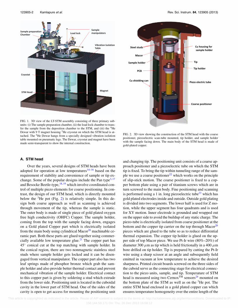
The overall schematic of our system is shown in Fig. 1.The LT-STM assembly consists of three primary sub-units: (i)The sample preparation chamber, (ii) the load lock chamber totransfer the sample from the deposition chamber to the STM,and (iii) the 4He dewar with 9 T magnet housing 3He cryostaton which the STM head is attached. The 4He dewar hangsfrom a specially designed vibration isolation table mountedon pneumatic legs. A combination of active and passive vi-bration isolation systems are used to obtain the required me-chanical stability of the tip. Data acquisition is done using thecommercial R9 SPM controller from RHK Technology.13 InSubsections II A–II G we describe the mechanical details ofvarious components of the setup.
This article is copyrighted as indicated in the article. Reuse of AIP content is subject to the terms at: http://scitationnew.aip.org/termsconditions. Downloaded to IP:
123905-2 Kamlapure et al. Rev. Sci. Instrum. 84, 123905 (2013)
FIG. 1. 3D view of the LT-STM assembly consisting of three primary sub-units: (i) The sample preparation chamber, (ii) the load lock chamber to trans-fer the sample from the deposition chamber to the STM, and (iii) the 4HeDewar with 9 T magnet housing 3He cryostat on which the STM head is at-tached. The 4He Dewar hangs from a specially designed vibration isolationtable mounted on pneumatic legs. The Dewar, cryostat and magnet have beenmade semi-transparent to show the internal construction.
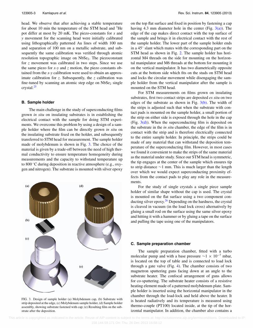
A. STM head
Over the years, several designs of STM heads have beenadopted for operation at low temperatures14–16 based on therequirement of stability and convenience of sample or tip ex-change. Some of the popular designs include the Pan type3, 17
and Besocke Beetle-type,18, 19 which involve coordinated con-trol of multiple piezo elements for coarse positioning. In con-trast, the design of our STM head, which is directly mountedbelow the 3He pot (Fig. 2) is relatively simple. In this de-sign both coarse approach as well as scanning is achievedthrough movement of the tip, whereas the sample is static.The outer body is made of single piece of gold plated oxygenfree high conductivity (OHFC) Copper. The sample holder,coming from the top with the sample facing down, engageson a Gold plated Copper part which is electrically isolatedfrom the main body using cylindrical Macor20 machinable ce-ramic part. Both these parts are glued together using commer-cially available low temperature glue.21 The copper part has45◦ conical cut at the top matching with sample holder. Inthe conical region, there are two nonmagnetic stainless steelstuds where sample holder gets locked and it can be disen-gaged from vertical manipulator. The copper part also has twoleaf springs made of phosphor bronze which grab the sam-ple holder and also provide better thermal contact and preventmechanical vibration of the sample holder. Electrical contactto this copper part is given by soldering a stud which extrudefrom the lower side. Positioning unit is located in the cuboidalcavity in the lower part of STM head. One of the sides of thecavity is open to get access for mounting the positioning unit
FIG. 2. 3D view showing the construction of the STM head with the coarsepositioner, piezoelectric scan-tube mounted, tip holder, and sample holderwith the sample facing down. The main body of the STM head is made ofgold-plated copper.
and changing tip. The positioning unit consists of a coarse ap-proach positioner and a piezoelectric tube on which the STMtip is fixed. To bring the tip within tunneling range of the sam-ple we use a coarse positioner22 which works on the principleof slip-stick motion. The coarse positioner is fixed to a cop-per bottom plate using a pair of titanium screws which are inturn screwed to the main body. Fine positioning and scanningis performed using a 1 in. long piezoelectric tube23 which hasgold plated electrodes inside and outside. Outside gold platingis divided into two segments. The lower half is used for Z mo-tion, while the upper segment has four quadrants and is usedfor XY motion. Inner electrode is grounded and wrapped outon the upper side to avoid the buildup of any static charge. Thepiezo-tube is electrically isolated from coarse positioner at thebottom and the copper tip carrier on the top through Macor20
pieces which are glued to the tube so as to reduce differentialthermal expansion. The copper tip holder is glued on the up-per side of top Macor piece. We use Pt-Ir wire (80%–20%) ofdiameter 300 μm as tip which is held frictionally in a 400 μmbore drilled on tip holder. Tip is prepared by cutting the Pt-Irwire using a sharp scissor at an angle and subsequently fieldemitted in vacuum at low temperature to achieve the desiredsharpness. Printed circuit boards screwed on the three sides ofthe cuboid serve as the connecting stage for electrical connec-tion to the piezo units, sample, and tip. Temperature of STMhead is measured using two CernoxTM sensors24 mounted onthe bottom plate of the STM as well as on the 3He pot. Theentire STM head enclosed in a gold plated copper can whichensures temperature homogeneity over the entire length of the
This article is copyrighted as indicated in the article. Reuse of AIP content is subject to the terms at: http://scitationnew.aip.org/termsconditions. Downloaded to IP:
158.144.59.171 On: Thu, 26 Dec 2013 16:58:12
123905-3 Kamlapure et al. Rev. Sci. Instrum. 84, 123905 (2013)
head. We observe that after achieving a stable temperaturefor about 10 min the temperature of the STM head and 3Hepot differ at most by 20 mK. The piezo-constants for x andy movement for the scanning head were initially calibratedusing lithographically patterned Au lines of width 100 nmand separation of 100 nm on a metallic substrate, and sub-sequently the same calibration was verified through atomicresolution topographic image on NbSe2. The piezoconstantfor z movement was calibrated in two steps. Since we usethe same piezo for x-y and z motion, the piezo constants ob-tained from the x-y calibration were used to obtain an approx-imate calibration for z. Subsequently, the z calibration wasfine-tuned by scanning an atomic step edge on NbSe2 singlecrystal.25
B. Sample holder
The main challenge in the study of superconducting filmsgrown in situ on insulating substrates is in establishing theelectrical contact with the sample for doing STM experi-ments. We overcome this problem by using a design of a sam-ple holder where the film can be directly grown in situ onthe insulating substrate fixed on the holder, and subsequentlytransferred to STM head for measurement. The sample holdermade of molybdenum is shown in Fig. 3. The choice of thematerial is given by a trade-off between the need of high ther-mal conductivity to ensure temperature homogeneity duringmeasurements and the capacity to withstand temperature upto 800 ◦C during deposition in reactive atmosphere (e.g., oxy-gen and nitrogen). The substrate is mounted with silver epoxy
(a) (d)
(e)
(b)
(c)
FIG. 3. Design of sample holder (a) Molybdenum cap, (b) Substrate withstrip deposited at the edge, (c) Molybdenum sample holder, (d) Sample holderassembly, showing substrate fastened with cap; (e) Resulting film on the sub-strate after the deposition.
on the top flat surface and fixed in position by fastening a caphaving 4.3 mm diameter hole in the center (Fig. 3(a)). Theedge of the cap makes direct contact with the top surface ofthe sample and brings it in electrical contact with the rest ofthe sample holder. The lower part of the sample holder endsin a 45◦ slant which mates with the corresponding part on theSTM head as shown in Fig. 2. The sample holder has hori-zontal M4 threads on the side for mounting on the horizon-tal manipulator and M6 threads at the bottom for mounting iton the vertical manipulator. It has two diametrically oppositecuts at the bottom side which fits on the studs on STM headand locks the circular movement while disengaging the sam-ple holder from the vertical manipulator after the sample ismounted on the STM head.
For STM measurements on films grown on insulatingsubstrates, first two contact strips are deposited ex situ on twoedges of the substrate as shown in Fig. 3(b). The width ofthe strips is adjusted such that when the substrate with con-tact pads is mounted on the sample holder, a small portion ofthe strip on either side is exposed through the hole in the cap(Fig. 3(d)). When the superconducting film is deposited onthe substrate in the in situ chamber, the edge of the film is incontact with the strip and is therefore electrically connectedto the entire sample holder. In principle, the strips could bemade of any material that can withstand the deposition tem-perature of the superconducting film. However, in most caseswe found it convenient to make the strips of the same materialas the material under study. Since our STM head is symmetric,the tip engages at the center of the sample which ensures tipto strip distance ∼1 mm. This is much larger than the lengthover which we would expect superconducting proximity ef-fects from the contact pads to play any role in the measure-ments.
For the study of single crystals a single piece sampleholder of similar shape without the cap is used. The crystalis mounted on the flat surface using a two component con-ducting silver epoxy.26 Depending on the hardness, the crystalis cleaved in vacuum (in the load lock cross) alternatively bygluing a small rod on the surface using the same silver epoxyand hitting it with a hammer or by gluing a tape on the surfaceand pulling the tape using one of the manipulators.
C. Sample preparation chamber
The sample preparation chamber, fitted with a turbomolecular pump and with a base pressure ∼1 × 10⁻⁷ mbar,is located on the top of table and is connected to load lockthrough a gate valve (Fig. 4). The chamber consists of twomagnetron sputtering guns facing down at an angle to thesubstrate heater. The confocal arrangement of guns allowsfor co-sputtering. The substrate heater consists of a resistiveheating element made of a patterned molybdenum plate. Sam-ple holder is inserted using the horizontal manipulator in thechamber through the load-lock and held above the heater. Itis heated radiatively and its temperature is measured usingthermo-couple (PT100) located inside, at the tip of the hor-izontal manipulator. In addition, the chamber also contains a
This article is copyrighted as indicated in the article. Reuse of AIP content is subject to the terms at: http://scitationnew.aip.org/termsconditions. Downloaded to IP:
158.144.59.171 On: Thu, 26 Dec 2013 16:58:12
123905-4 Kamlapure et al. Rev. Sci. Instrum. 84, 123905 (2013)
FIG. 4. Schematic 3D view of the sample preparation chamber and load-lockcross. The deposition chamber incorporates two magnetron sputtering guns,a substrate heater for heating the substrate up to 800 ◦C, a plasma ion etchinggun and two thermal evaporation sources. The substrate is inserted inside thedeposition chamber using the horizontal manipulator.
plasma ion source27 for cleaning substrates prior to depositionand two tungsten boats for thermal evaporation.
D. Load lock and sample manipulators
The load-lock, located at the top of the 3He cryostat,has six CF35 ports and it is connected to sample prepara-tion chamber and STM chamber through gate valves. Typi-cal time to pump the load-lock chamber from ambient pres-sure to 1 × 10⁻⁶ mbar is about 20 min. Sample manipulators(Fig. 5) are made of seamless steel tubes (closed at one end)and have matching threads at the end to engage on the cor-responding threads on the sample holder. A thermocouple isfitted inside the horizontal sample manipulator to measure thetemperature of the sample during deposition. Once the sam-ple is deposited horizontal manipulator is pulled back bring-ing the sample holder in the cross, and the sample holder istransferred to vertical manipulator and inserted into the STMhead.
FIG. 5. Design of the horizontal sample manipulator with in-built thermo-couple for measuring the temperature during sample deposition. A differen-tial pumping arrangement between two Wilson seals is used to remove anyleaked gas during movement. The end of the manipulator is made transparentto show the position of the thermocouple. The vertical manipulator is similarin construction but does not have the thermocouple.
FIG. 6. Schematic view of the 3He cryostat inside the 4He dewar showingthe sorption pump, 1 K pot, 3He pot and the STM head which is bolted belowthe 3He pot. The liquid 4He Dewar has a capacity of 65 l and a retention timeof 5 days.
E. Cryostat and temperature control of the sample
The low temperature stage consists of an internally fittedcharcoal sorption pump based 3He cryostat from Janis Re-search Company28 (Fig. 6). We use a custom design with an-nular shaped sorption pump, 1 K pot, and 3He pot which giveus direct line of site access from the top of the cryostat to theSTM head mounted below the 3He pot. To ensure thermal sta-bility the STM head is bolted to 3He pot using 6 screws whichensure good thermal contact between the two. To prevent ra-diative heating, a radiation plug is inserted in the cryostat afterloading the sample using the same vertical manipulator as theone used to insert the sample. The radiation plug (not shown)sits just above the STM head. The 3He pot and sorption pumpare fitted with resistive heaters. All electrical wires comingfrom the top are thermally anchored at the 1 K pot and the 3Hepot. The entire process of cooling the STM from 4.2 K to thebase temperature of 350 mK takes about 20 min with a holdtime of about 8 h. We wait for about 15 min - after the basetemperature is reached before starting our measurements. Be-tween the base temperature and 3 K, we control the tempera-ture by controlling the temperature of the sorption pump. Forstabilizing above 3 K we use the resistive heater fitted on the3He pot by keeping the sorption pump temperature constantat 30 K.
F. Liquid helium Dewar
The cryostat is mounted in a 65 l capacity Al-FibreglassDewar with retention time of ∼5 days. The superconducting
This article is copyrighted as indicated in the article. Reuse of AIP content is subject to the terms at: http://scitationnew.aip.org/termsconditions. Downloaded to IP:
158.144.59.171 On: Thu, 26 Dec 2013 16:58:12
123905-5 Kamlapure et al. Rev. Sci. Instrum. 84, 123905 (2013)
magnet with maximum field of 9 T aligned along the STM tiphangs from the top flange of the cryostat. Exhaust line of thecryostat is connected with one way valve which maintains aconstant pressure slightly above atmosphere. This allows usto flow liquid 4He in a capillary wrapped around the sorptionpump such that the sorption pump can be cooled without us-ing an external pump.
To reduce the electrical noise coming from the 50 Hz linesignal, ground connection of all instruments, table, and De-war are made to a separate master ground. RF noise is furtherreduced by introducing 10 MHz low pass filter before eachconnection that goes into the STM. The tunneling current isdetected using a Femto DLPCA-200 current amplifier placedat the top of the cryostat with gain of 109 V/A. While thebandwidth of the DLCPA-200 amplifier is 500 kHz, the mea-
0 25 50 75 100100
101
102
103
0 25 50 75 100
101
102
103
0 50 100 150 200
101
102
103
Vel
oci
ty (
nm
s-1 H
z-1/2)
Frequency (Hz)
1K pot pumping on1K pot pumping off
(a)
curr
ent
SD
(fA
Hz-1
/2)
Frequency (Hz)
Tip engaged (Feedback off)Tip engaged (Feedback on)Tip retracted
(b)
Z (
fm H
z-1/2)
Frequency (Hz)
(c)
FIG. 7. (a) Spectral density of the velocity vs. frequency on the top of thecryostat measured using an accelerometer. The spectral densities with andwithout the 1 K pot pump on are nearly identical. (b) Spectral density of thetunneling current with the tip out of tunneling range, within tunneling rangewith feedback on and with feedback off. (c) Spectral density of Z heightsignal with feedback on. Measurements in (b) and (c) were performed at 350mK on a NbSe2 single crystal with tunneling current set to 50 pA and biasvoltage to 20 mV.
surement bandwidth is set digitally restricted to 2.5 kHz in theR9 SPM controller.
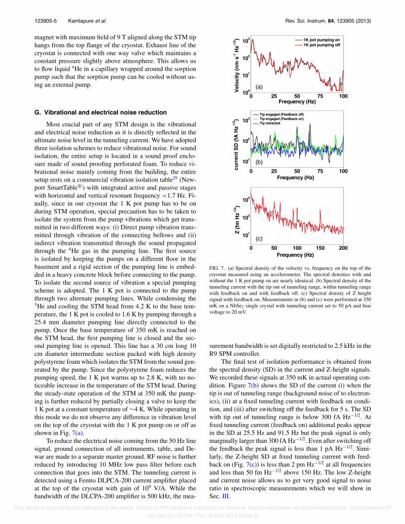
The final test of isolation performance is obtained fromthe spectral density (SD) in the current and Z-height signals.We recorded these signals at 350 mK in actual operating con-dition. Figure 7(b) shows the SD of the current (i) when thetip is out of tunneling range (background noise of to electron-ics), (ii) at a fixed tunneling current with feedback on condi-tion, and (iii) after switching off the feedback for 5 s. The SDwith tip out of tunneling range is below 300 fA Hz−1/2. Atfixed tunneling current (feedback on) additional peaks appearin the SD at 25.5 Hz and 91.5 Hz but the peak signal is onlymarginally larger than 300 fA Hz−1/2. Even after switching offthe feedback the peak signal is less than 1 pA Hz−1/2. Simi-larly, the Z-height SD at fixed tunneling current with feed-back on (Fig. 7(c)) is less than 2 pm Hz−1/2 at all frequenciesand less than 50 fm Hz−1/2 above 150 Hz. The low Z-heightand current noise allows us to get very good signal to noiseratio in spectroscopic measurements which we will show inSec. III.
This article is copyrighted as indicated in the article. Reuse of AIP content is subject to the terms at: http://scitationnew.aip.org/termsconditions. Downloaded to IP:
158.144.59.171 On: Thu, 26 Dec 2013 16:58:12
123905-6 Kamlapure et al. Rev. Sci. Instrum. 84, 123905 (2013)
-4 -2 0 2 40
1
2
G(V
)/G
(5 m
V)
V(mV)
data BCS fit
Δ=1.3 meV
FIG. 8. Tunneling spectroscopy on Pb single crystal acquired with Pt-Ir tipat 500 mK along with BCS fit. The spectrum is averaged over 10 voltagesweeps at the same point. The spectroscopy set point before switching off thefeedback was V = 6 mV, I = 500 pA, and the lock-in modulation voltage was150 μV with frequency of 419.3 Hz.
III. STM PERFORMANCE
In this section we demonstrate the spatial and energy res-olution of our LT-STM through measurements on Pb singlecrystal, NbSe2 single crystal, and NbN thin films.
A. Tunneling spectroscopy on Pb
To characterize the energy resolution of our system thetunneling spectrum was acquired on a Pb single crystal. Forspectroscopy dI/dV vs. V is measured with feedback switchedoff using standard modulation technique using an internallock-in amplifier built-in within our main control unit (R9,
0.0 0.5 1.0 1.5 2.0 2.5
0
10
20
30
0
10
20
30
40
Hei
gh
t (p
m)
Distance (nm)
Lattice constant = 3.3 (b)
Z (
pm
)
(a)
FIG. 9. (a) Atomically resolved topographic image of NbSe2 obtained inconstant current mode; the charge density wave modulation is also visible.The tunneling current was set to 150 pA, the bias voltage to 20 mV, and thescan speed was 13 nm/s. (b) Line cut along the line shown in (a).
RHK technology). Figure 8 shows the typical spectrum ac-quired at 500 mK at a single point on polished Pb singlecrystal using modulation voltage of 150 μV and frequency of419.3 Hz. We have verified that the tunneling spectra do notshow any noticeable variation when modulation frequencyis varied from 400 Hz to 2.5 kHz. Figure 8 also shows the
FIG. 10. Vortex imaging on NbSe2. (a)-(d) 64 × 64 conductance maps over 352 × 352 nm area at different voltages at 350 mK in an applied field of 200 mT.The maps are obtained from full spectroscopic scans from −6 mV to 6 mV at each pixel. (e) Line scan of the tunneling spectra along the white line marked inpanel (a). Three spectra inside (2) and outside (1 & 3) vortex cores are highlighted in black. (f) High resolution conductance map acquired over the same areaby scanning at fixed bias of V = 1.4 mV; the tunneling current was set to 50 pA and modulation voltage was set to 150 μV with frequency of 2.3 kHz.
This article is copyrighted as indicated in the article. Reuse of AIP content is subject to the terms at: http://scitationnew.aip.org/termsconditions. Downloaded to IP:
158.144.59.171 On: Thu, 26 Dec 2013 16:58:12
123905-7 Kamlapure et al. Rev. Sci. Instrum. 84, 123905 (2013)
fit using Bardeen-Cooper-Schrieffer theory for tunneling con-ductance which is described by the tunneling equation givenby30
G(V ) = dI
dV
∣∣∣∣V
= d
dV
×⎧⎨⎩
1
RN
∞∫−∞
NS (E)[f (E) − f (E − eV )
]dE
⎫⎬⎭ ,
where NS (E) = Re{ |E|√(|E|)2−�2
}. We have taken into account
broadening due to the finite modulation voltage which isused for lock-in measurements by doing adjacent averagingof points in the theoretical curve over a sliding voltage rangeof 150 μV. BCS fit gives an energy gap � = 1.3 meV whichis in good agreement31 with reported values of the energy gapin Pb.
B. Atomic resolution and vortex imaging on NbSe2
To test our system for atomic resolution and in mag-netic field, we performed measurements on a 2H-NbSe2 sin-gle crystal. Having a hexagonal closed packed layered struc-ture this crystal can be easily cleaved in-plane. We cleavedthe crystal in situ by attaching a tape on the surface andsubsequently pulling the tape in vacuum in the load-lockchamber using the sample manipulators. Figure 9 showsthe atomic resolution image at 350 mK which reveals thehexagonal lattice structure along with the charge densitywave modulation. The lattice spacing of 0.33 nm is in goodagreement with the lattice constant of NbSe2 known fromliterature.9, 32, 33
For imaging the vortex state, we have first taken full areaspectroscopic map over an area of 352 × 352 nm in mag-netic field of 200 mT at 350 mK. In this measurement werecorded the spatially resolved tunneling spectra (dI/dV vs. V)at each point of a grid having 64 × 64 pixels by sweeping thebias from 6 mV to −6mV. Figures 10(a)–10(d) show inten-sity plots of the tunneling conductance normalized at 6 mVat different bias voltages, showing the hexagonal vortex lat-tice. The lattice constant, a ≈ 109.8 nm, is in excellent agree-ment with the theoretical value expected from Ginzburg Lan-dau theory.25, 30 For voltages below �/e the vortices appear asregions with larger conductance, whereas for voltages close tothe coherence peak the vortices appear as regions with lowerconductance. Figure 10(e) shows the line scan sectioned onthe line shown in Fig. 10(a). Three representative spectra arehighlighted in the figure. Spectra 1 and 3 correspond to thesuperconducting region, while the spectrum 2 is at the vor-tex core and has a zero bias conductance peak which is thesignature of Andreev bound state inside the vortex core. InFig. 10(f) we show a high resolution (128 × 128) conduc-tance map obtained by measuring dI/dV at a fixed bias voltageof 1.4 mV while scanning over the same area.
C. Scanning tunneling spectroscopy on disorderedNbN thin film
As an example of a measurement on thin films we showspatially resolved STS measurements on a disordered epitax-
-6 -4 -2 0 2 4 60.0
0.4
0.8
1.2 (c)
V(mV)
G(V
)/G
(6m
V)
V(mV)
Po
siti
on
(nm
)200
100
0
1.2
0.6
0-6 0 6
0.4 0.8 1.2G(V)/G(6mV)
0
1
2
3
(b)
Z (
nm
)
(a)
FIG. 11. STS data for NbN thin film with Tc = 6.4 K. (a) The topography ofthe surface over 200 × 200 nm area acquired in constant current mode. Thetunneling current was set to 400 pA, the bias voltage to 8 mV, and the scanspeed was 30 nm/s. (b) Normalized tunneling spectra along the horizontaldashed line in panel (a). (c) Normalized average tunneling spectrum over 200× 200 nm area. The modulation voltage was set to 150 μV and modulationfrequency to 2 KHz.
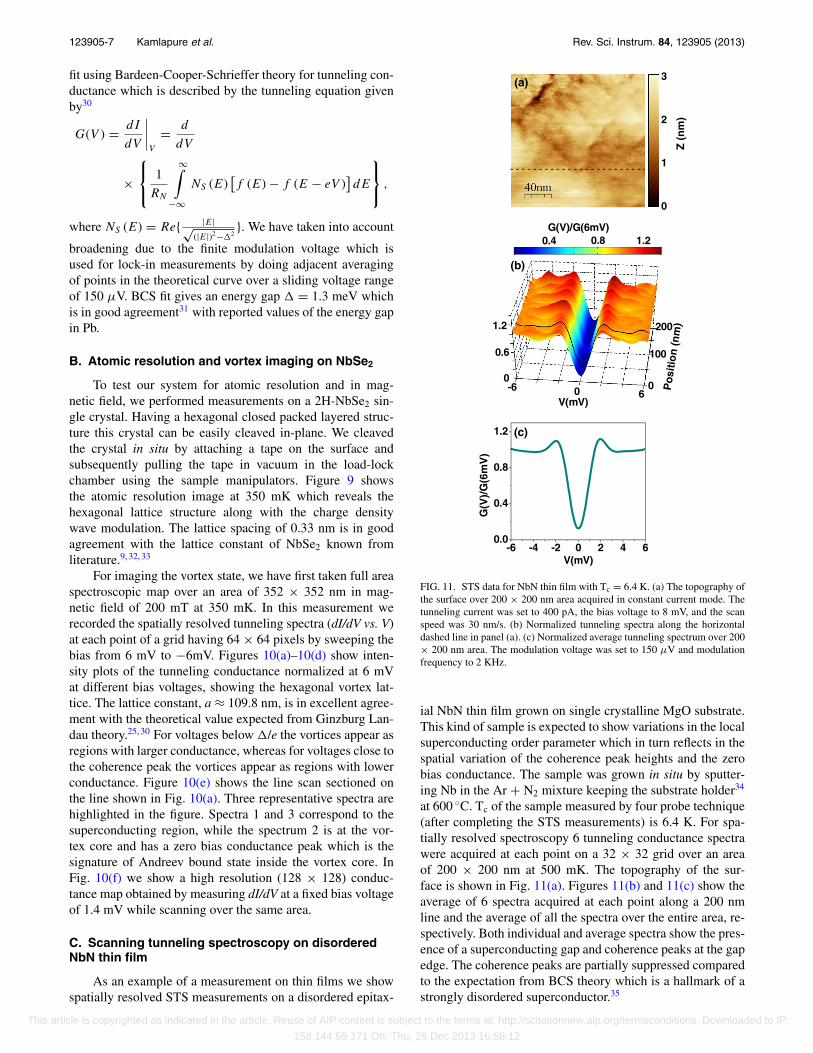
ial NbN thin film grown on single crystalline MgO substrate.This kind of sample is expected to show variations in the localsuperconducting order parameter which in turn reflects in thespatial variation of the coherence peak heights and the zerobias conductance. The sample was grown in situ by sputter-ing Nb in the Ar + N2 mixture keeping the substrate holder34
at 600 ◦C. Tc of the sample measured by four probe technique(after completing the STS measurements) is 6.4 K. For spa-tially resolved spectroscopy 6 tunneling conductance spectrawere acquired at each point on a 32 × 32 grid over an areaof 200 × 200 nm at 500 mK. The topography of the sur-face is shown in Fig. 11(a). Figures 11(b) and 11(c) show theaverage of 6 spectra acquired at each point along a 200 nmline and the average of all the spectra over the entire area, re-spectively. Both individual and average spectra show the pres-ence of a superconducting gap and coherence peaks at the gapedge. The coherence peaks are partially suppressed comparedto the expectation from BCS theory which is a hallmark of astrongly disordered superconductor.35
This article is copyrighted as indicated in the article. Reuse of AIP content is subject to the terms at: http://scitationnew.aip.org/termsconditions. Downloaded to IP:
158.144.59.171 On: Thu, 26 Dec 2013 16:58:12
123905-8 Kamlapure et al. Rev. Sci. Instrum. 84, 123905 (2013)
IV. SUMMARY
In summary, we have presented a relatively simple designof a 3He refrigerator based STM operating down to 350 mKand in magnetic fields up to 9 T. Using a novel design forsample holder and STM head we demonstrate the capabilityto perform STM and STS measurements on in situ cleavedsingle crystals and in situ grown thin films.
ACKNOWLEDGMENTS
We would like to thank Supriya Dhawde for preparingthe 3D drawing of the experimental systems, Parasharam Shi-rage and A Thamizhavel for providing the NbSe2 single crys-tals, John Jesudasan for providing the optimal conditions fordeposition of NbN thin films, and Sourin Mukhopadhyay forbeing involved in the fabrication of an early 4He version of theSTM. The work was supported by the Department of AtomicEnergy, Government of India.
1G. Binnig, H. Rohrer, Ch. Gerber, and E. Weibel, Phys. Rev. Lett. 50, 120(1983); Appl. Phys. Lett. 40, 178 (1982).
2G. Binnig and H. Rohrer, Surf. Sci. 126, 236 (1983).3S. H. Pan, E. W. Hudson, and J. C. Davis, Rev. Sci. Instrum. 70, 1459(1999).
4M. Assig, M. Etzkorn, A. Enders, W. Stiepany, C. R. Ast, and K. Kern,Rev. Sci. Instrum. 84, 033903 (2013).
5L. Zhang, T. Miyamachi, T. Tomanic, R. Dehm, and W. Wulfhekel, Rev.Sci. Instrum. 82, 103702 (2011).
6Y. J. Song, A. F. Otte, V. Shvarts, Z. Zhao, Y. Kuk, S. R. Blankenship,A. Band, F. M. Hess, and J. A. Stroscio, Rev. Sci. Instrum. 81, 121101(2010).
7M. Kugler, C. Renner, Ø. Fischer, V. Mikheev, and G. Batey, Rev. Sci.Instrum. 71, 1475 (2000).
8C. Debuschewitz, F. Münstermann, V. Kunej, and E. Scheer, J. Low Temp.Phys. 147, 525 (2007).
9H. Kambara, T. Matsui, Y. Niimi, and H. Fukuyama, Rev. Sci. Instrum. 78,073703 (2007).
10U. R. Singh, M. Enayat, S. C. White, and P. Wahl, Rev. Sci. Instrum. 84,013708 (2013).
11J. Wiebe, A. Wachowiak, F. Meier, D. Haude, T. Foster, M. Morgenstern,and R. Wiesendanger, Rev. Sci. Instrum. 75, 4871 (2004).
12N. Moussy, H. Courtois, and B. Pannetier, Rev. Sci. Instrum. 72, 128(2001).
13Control electronics from RHK technology, Inc., USA. Model: R9 SPMControl system.
14S.-i. Park and C. F. Quate, Rev. Sci. Instrum. 58, 2010 (1987).15G. Meyer, Rev. Sci. Instrum. 67, 2960 (1996).16S. J. Ball, G. E. Contant, and A. B. McLean, Rev. Sci. Instrum. 75, 5293
(2004).17Chr. Wittneven, R. Dombrowski, S. H. Pan, and R. Wiesendanger, Rev. Sci.
Instrum. 68, 3806 (1997).18K. Besocke, Surf. Sci. 181, 145 (1987).19J. Frohn, J. F. Wolf, K. Besocke, and M. Teske, Rev. Sci. Instrum. 60, 1200
(1989).20Machinable ceramic from Corning Glass Corporation (http://www.corning.
com/specialtymaterials/products_capabilites/macor.aspx)21Low temperature glue, STYCAST 2850FT, from Emerson and Cuming.22Coarse positioner from Attocube Systems AG (model ANPz51).23Piezo electric tube from EBL Products, Model EBL#224Cernox sensor from LakeShore Cryotronics Inc., USA.25See supplementary material at http://dx.doi.org/10.1063/1.4849616 for de-
tails on Z calibration and for the variation of vortex lattice constant as afunction of magnetic field.
USA.30M. Tinkham Introduction to Superconductivity (Dover Publications Inc.,
Mineola, New York, 2004).31I. Giaever and K. Megerle, Phys. Rev. 122, 1101 (1961).32R. V. Coleman, B. Giambattista, A. Johnson, W. W. McNairy, G.
Slough, P. K. Hansma, and B. Drake, J. Vac. Sci. Technol., A 6, 338(1988).
33M. Marz, G. Goll, and H. v. Löhneysen, Rev. Sci. Instrum. 81, 045102(2010).
34S. P. Chockalingam, M. Chand, A. Kamlapure, J. Jesudasan, A. Mishra, V.Tripathi, and P. Raychaudhuri, Phys. Rev. B 77, 214503 (2008).
35A. Kamlapure, T. Das, S. C. Ganguli, J. B. Parmar, S. Bhattacharyya, andP. Raychaudhuri, Sci. Rep. 3, 2979 (2013).
This article is copyrighted as indicated in the article. Reuse of AIP content is subject to the terms at: http://scitationnew.aip.org/termsconditions. Downloaded to IP: