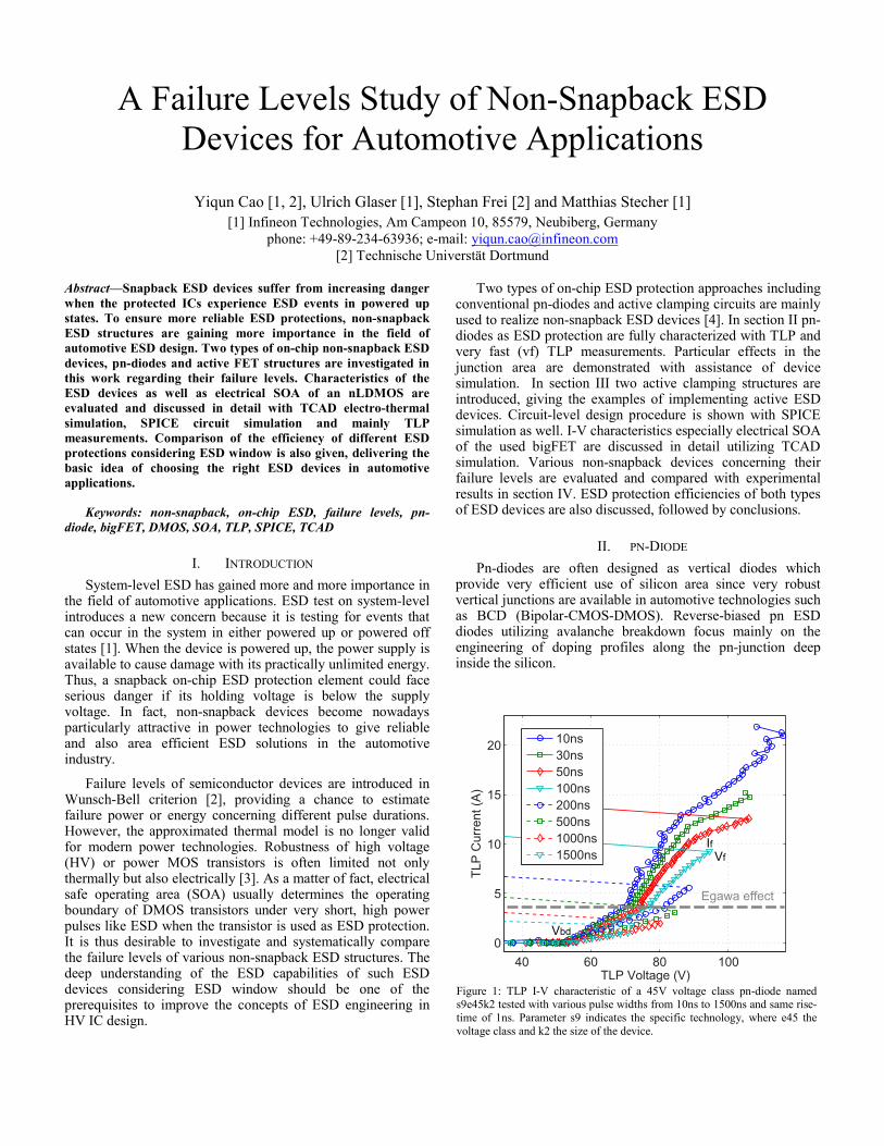
A Failure Levels Study of Non-Snapback ESD Devices for Automotive Applications Yiqun Cao [1, 2], Ulrich Glaser [1], Stephan Frei [2] and Matthias Stecher [1] [1] Infineon Technologies, Am Campeon 10, 85579, Neubiberg, Germany phone: +49-89-234-63936; e-mail: [email protected][2] Technische Universtät Dortmund Abstract—Snapback ESD devices suffer from increasing danger when the protected ICs experience ESD events in powered up states. To ensure more reliable ESD protections, non-snapback ESD structures are gaining more importance in the field of automotive ESD design. Two types of on-chip non-snapback ESD devices, pn-diodes and active FET structures are investigated in this work regarding their failure levels. Characteristics of the ESD devices as well as electrical SOA of an nLDMOS are evaluated and discussed in detail with TCAD electro-thermal simulation, SPICE circuit simulation and mainly TLP measurements. Comparison of the efficiency of different ESD protections considering ESD window is also given, delivering the basic idea of choosing the right ESD devices in automotive applications. Keywords: non-snapback, on-chip ESD, failure levels, pn- diode, bigFET, DMOS, SOA, TLP, SPICE, TCAD I. INTRODUCTION System-level ESD has gained more and more importance in the field of automotive applications. ESD test on system-level introduces a new concern because it is testing for events that can occur in the system in either powered up or powered off states [1]. When the device is powered up, the power supply is available to cause damage with its practically unlimited energy. Thus, a snapback on-chip ESD protection element could face serious danger if its holding voltage is below the supply voltage. In fact, non-snapback devices become nowadays particularly attractive in power technologies to give reliable and also area efficient ESD solutions in the automotive industry. Failure levels of semiconductor devices are introduced in Wunsch-Bell criterion [2], providing a chance to estimate failure power or energy concerning different pulse durations. However, the approximated thermal model is no longer valid for modern power technologies. Robustness of high voltage (HV) or power MOS transistors is often limited not only thermally but also electrically [3]. As a matter of fact, electrical safe operating area (SOA) usually determines the operating boundary of DMOS transistors under very short, high power pulses like ESD when the transistor is used as ESD protection. It is thus desirable to investigate and systematically compare the failure levels of various non-snapback ESD structures. The deep understanding of the ESD capabilities of such ESD devices considering ESD window should be one of the prerequisites to improve the concepts of ESD engineering in HV IC design. Two types of on-chip ESD protection approaches including conventional pn-diodes and active clamping circuits are mainly used to realize non-snapback ESD devices [4]. In section II pn- diodes as ESD protection are fully characterized with TLP and very fast (vf) TLP measurements. Particular effects in the junction area are demonstrated with assistance of device simulation. In section III two active clamping structures are introduced, giving the examples of implementing active ESD devices. Circuit-level design procedure is shown with SPICE simulation as well. I-V characteristics especially electrical SOA of the used bigFET are discussed in detail utilizing TCAD simulation. Various non-snapback devices concerning their failure levels are evaluated and compared with experimental results in section IV. ESD protection efficiencies of both types of ESD devices are also discussed, followed by conclusions. II. PN-DIODE Pn-diodes are often designed as vertical diodes which provide very efficient use of silicon area since very robust vertical junctions are available in automotive technologies such as BCD (Bipolar-CMOS-DMOS). Reverse-biased pn ESD diodes utilizing avalanche breakdown focus mainly on the engineering of doping profiles along the pn-junction deep inside the silicon. 40 60 80 100 0 5 10 15 20 TLP Voltage (V) TLP Current (A) 10ns 30ns 50ns 100ns 200ns 500ns 1000ns 1500ns Egawa effect Vf If Vbd Figure 1: TLP I-V characteristic of a 45V voltage class pn-diode named s9e45k2 tested with various pulse widths from 10ns to 1500ns and same rise- time of 1ns. Parameter s9 indicates the specific technology, where e45 the voltage class and k2 the size of the device.
Transcript
A Failure Levels Study of Non-Snapback ESD Devices for Automotive Applications
Yiqun Cao [1, 2], Ulrich Glaser [1], Stephan Frei [2] and Matthias Stecher [1] [1] Infineon Technologies, Am Campeon 10, 85579, Neubiberg, Germany
Abstract—Snapback ESD devices suffer from increasing danger when the protected ICs experience ESD events in powered up states. To ensure more reliable ESD protections, non-snapback ESD structures are gaining more importance in the field of automotive ESD design. Two types of on-chip non-snapback ESD devices, pn-diodes and active FET structures are investigated in this work regarding their failure levels. Characteristics of the ESD devices as well as electrical SOA of an nLDMOS are evaluated and discussed in detail with TCAD electro-thermal simulation, SPICE circuit simulation and mainly TLP measurements. Comparison of the efficiency of different ESD protections considering ESD window is also given, delivering the basic idea of choosing the right ESD devices in automotive applications.
I. INTRODUCTION System-level ESD has gained more and more importance in
the field of automotive applications. ESD test on system-level introduces a new concern because it is testing for events that can occur in the system in either powered up or powered off states [1]. When the device is powered up, the power supply is available to cause damage with its practically unlimited energy. Thus, a snapback on-chip ESD protection element could face serious danger if its holding voltage is below the supply voltage. In fact, non-snapback devices become nowadays particularly attractive in power technologies to give reliable and also area efficient ESD solutions in the automotive industry.
Failure levels of semiconductor devices are introduced in Wunsch-Bell criterion [2], providing a chance to estimate failure power or energy concerning different pulse durations. However, the approximated thermal model is no longer valid for modern power technologies. Robustness of high voltage (HV) or power MOS transistors is often limited not only thermally but also electrically [3]. As a matter of fact, electrical safe operating area (SOA) usually determines the operating boundary of DMOS transistors under very short, high power pulses like ESD when the transistor is used as ESD protection. It is thus desirable to investigate and systematically compare the failure levels of various non-snapback ESD structures. The deep understanding of the ESD capabilities of such ESD devices considering ESD window should be one of the prerequisites to improve the concepts of ESD engineering in HV IC design.
Two types of on-chip ESD protection approaches including conventional pn-diodes and active clamping circuits are mainly used to realize non-snapback ESD devices [4]. In section II pn-diodes as ESD protection are fully characterized with TLP and very fast (vf) TLP measurements. Particular effects in the junction area are demonstrated with assistance of device simulation. In section III two active clamping structures are introduced, giving the examples of implementing active ESD devices. Circuit-level design procedure is shown with SPICE simulation as well. I-V characteristics especially electrical SOA of the used bigFET are discussed in detail utilizing TCAD simulation. Various non-snapback devices concerning their failure levels are evaluated and compared with experimental results in section IV. ESD protection efficiencies of both types of ESD devices are also discussed, followed by conclusions.
II. PN-DIODE Pn-diodes are often designed as vertical diodes which
provide very efficient use of silicon area since very robust vertical junctions are available in automotive technologies such as BCD (Bipolar-CMOS-DMOS). Reverse-biased pn ESD diodes utilizing avalanche breakdown focus mainly on the engineering of doping profiles along the pn-junction deep inside the silicon.
40 60 80 1000
5
10
15
20
TLP Voltage (V)
TLP
Cur
rent
(A)
10ns30ns50ns100ns200ns500ns1000ns1500ns
Egawa effect
VfIf
Vbd
Figure 1: TLP I-V characteristic of a 45V voltage class pn-diode named s9e45k2 tested with various pulse widths from 10ns to 1500ns and same rise-time of 1ns. Parameter s9 indicates the specific technology, where e45 the voltage class and k2 the size of the device.
Figure 1 shows the TLP measurement results for a 45V class pn-diode. The TLP voltage and current are generated by averaging the whole pulse duration in order to take self-heating of junction especially for long pulses into account. The rise-time is not relevant as it didn’t change the results in a practical manner. Note that Vf, If and Vbd indicate failure voltage, failure current and breakdown voltage, respectively. TLP test with 5ns pulse width was also performed but not explicit plotted since the device did not fail within the test hardware limitation of 30A maximum current. For pulse widths smaller than 200ns, the current density in the pn junction reaches the level where Egawa effect [5] takes place and changes the slope of I-V characteristic of the device. The slope changing points according to the tests with different pulse durations generate the nearly horizontal dashed line (Figure 1), which confirms the current density level is the main condition to enable Egawa effect around the pn junction area. To give a detailed observation of this phenomenon, 1-D TCAD simulation is sufficient to show qualitatively the behavior of the pn-diode. Figure 2 shows the simulation results where the second local maximum of electric field appears with the higher current density.
Egawa effect surely improves the ESD performance of the diode since it can lower the total on-resistance regarding ESD (Ron) of the device, resulting in improvement of on-chip area efficiency. In this work, several pn-diodes implemented for two voltage classes were characterized using the same TLP test method discussed above. If one simply defines Ron as (Vf -Vbd)/If, the dependence of Ron area product on the pulse duration can be derived from the measurement results as depicted in Figure 3. As expected, the diodes with the same breakdown voltage have nearly the same Ron referring to unit area. However, the pn-diodes in higher voltage classes have to be designed larger to sustain the same Ron. The weak doping concentration in p-tub region [4] increases the resistance in the current path significantly while adjusting a higher breakdown voltage. This results in less area efficiency of 45V devices with a factor of approximately 1.8 comparing to 25V diodes.
As a matter of fact, in high voltage applications ESD design windows often have upper limits of several tens of volts as constraints. Hence very high Vf is out of concern for real ESD design. Effective Ron in terms of ESD window rather than thermal Vf is a more practical measure which probably will reduce the area efficiency of pn-diodes. Nevertheless, failure power or energy versus pulse duration is interesting for the investigation of junction robustness. Figure 4 shows the characteristics of energy and power to failure of various ESD diodes. Overlapped lines imply the fact that failure levels of the pn-diodes are relatively independent on the voltage classes within the given technology and proper designs. Linear power and energy to failure per area in double logarithm plot basically confirm the Wunsch-Bell theory. However, the slope is approximately -0.8 in the reality in double logarithm plot rather than -0.5 according to Wunsch thermal model. 1015
1016
1017
1018
1019
1020
1021
1E5
2E5
3E5
Anode Cathode
Abs
olut
e D
opin
g C
once
ntra
tion
(cm
)-3
Absolute E
lectric Field (V/m
)
p+
p-tub region
n+
I=2mAI=5mA
Figure 2: 1-D TCAD simulation for the pn-diode in the reverse-biased condition shows the differences in the electric field with or without Egawa effect. Doping profile is shown as well. With 2mA current biasing, only one local electric field maximum exists along the diode from anode to cathode, where double peaks are observed at 5mA bias current. The higher hole and electron current densities lead to the space charge modification, resulting in double peaks of electric field.
Figure 3: Ron area product versus pulse duration for two groups of pn-diodes in 25V and 45V voltage classes. k1 to k4 denotes chip area of the devices with the relation k4≈2k2≈4k1.
Figure 4: Energy and power to failure per area versus pulse duration for two groups of pn-diodes in 25V and 45V voltage classes.
III. ACTIVE CLAMPING STRUCTURE Another common approach for non-snapback on-chip ESD
protection utilizes an active controlled bigFET [4]. RC triggered HV-MOS ESD circuits have been applied in the advanced CMOS world for years [7]. To avoid the risks of wrong dynamic triggering due to EOS disturbances, static triggering concept is preferred in automotive HV ESD design field.
A. Design and evaluation of active clamping structures
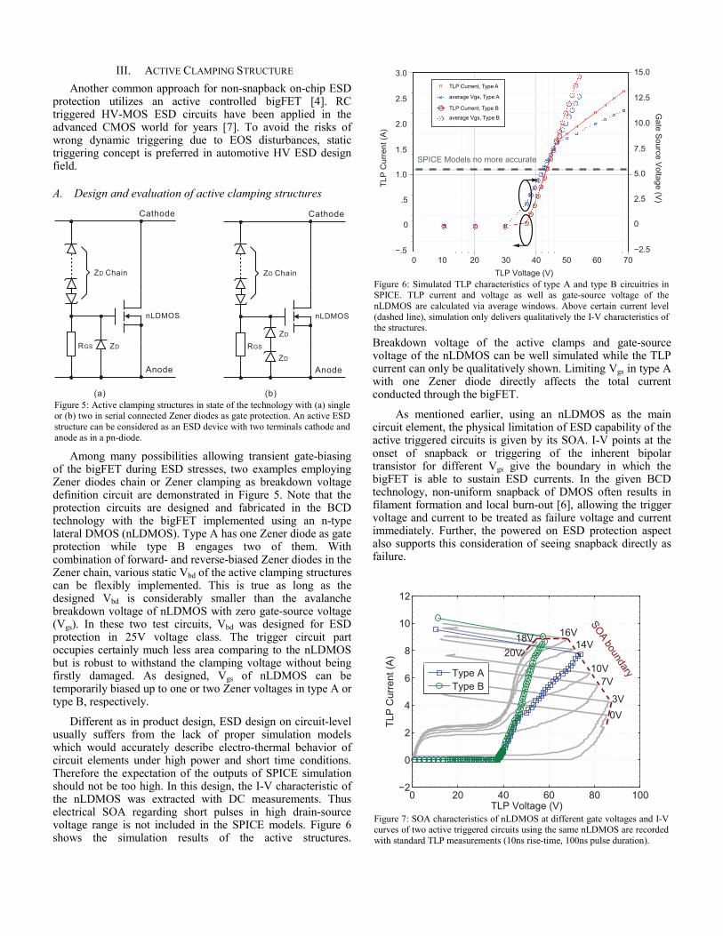
Among many possibilities allowing transient gate-biasing of the bigFET during ESD stresses, two examples employing Zener diodes chain or Zener clamping as breakdown voltage definition circuit are demonstrated in Figure 5. Note that the protection circuits are designed and fabricated in the BCD technology with the bigFET implemented using an n-type lateral DMOS (nLDMOS). Type A has one Zener diode as gate protection while type B engages two of them. With combination of forward- and reverse-biased Zener diodes in the Zener chain, various static Vbd of the active clamping structures can be flexibly implemented. This is true as long as the designed Vbd is considerably smaller than the avalanche breakdown voltage of nLDMOS with zero gate-source voltage (Vgs). In these two test circuits, Vbd was designed for ESD protection in 25V voltage class. The trigger circuit part occupies certainly much less area comparing to the nLDMOS but is robust to withstand the clamping voltage without being firstly damaged. As designed, Vgs of nLDMOS can be temporarily biased up to one or two Zener voltages in type A or type B, respectively.
Different as in product design, ESD design on circuit-level usually suffers from the lack of proper simulation models which would accurately describe electro-thermal behavior of circuit elements under high power and short time conditions. Therefore the expectation of the outputs of SPICE simulation should not be too high. In this design, the I-V characteristic of the nLDMOS was extracted with DC measurements. Thus electrical SOA regarding short pulses in high drain-source voltage range is not included in the SPICE models. Figure 6 shows the simulation results of the active structures.
Breakdown voltage of the active clamps and gate-source voltage of the nLDMOS can be well simulated while the TLP current can only be qualitatively shown. Limiting Vgs in type A with one Zener diode directly affects the total current conducted through the bigFET.
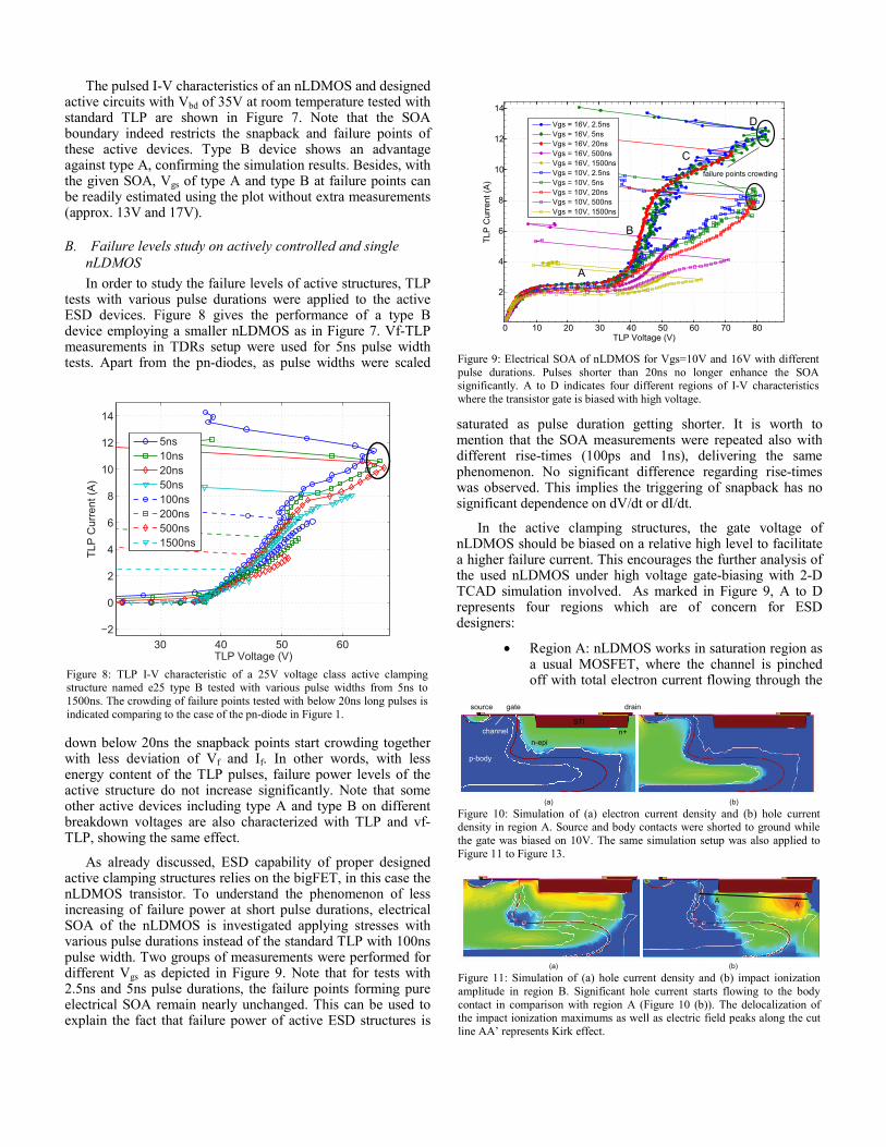
As mentioned earlier, using an nLDMOS as the main circuit element, the physical limitation of ESD capability of the active triggered circuits is given by its SOA. I-V points at the onset of snapback or triggering of the inherent bipolar transistor for different Vgs give the boundary in which the bigFET is able to sustain ESD currents. In the given BCD technology, non-uniform snapback of DMOS often results in filament formation and local burn-out [6], allowing the trigger voltage and current to be treated as failure voltage and current immediately. Further, the powered on ESD protection aspect also supports this consideration of seeing snapback directly as failure.
Cathode
Anode
RGS
Z ChainD
nLDMOS
ZD
Cathode
Anode
RGS
Z ChainD
nLDMOS
ZD
(a) (b)
ZD
Figure 5: Active clamping structures in state of the technology with (a) single or (b) two in serial connected Zener diodes as gate protection. An active ESD structure can be considered as an ESD device with two terminals cathode and anode as in a pn-diode.
0 20 40 60 80 100−2
0
2
4
6
8
10
12
TLP
Cur
rent
(A)
TLP Voltage (V)
3V0V
Type AType B
20V18V 16V
14V
10V7V
SOA boundary
Figure 7: SOA characteristics of nLDMOS at different gate voltages and I-V curves of two active triggered circuits using the same nLDMOS are recorded with standard TLP measurements (10ns rise-time, 100ns pulse duration).
TLP Current, Type A
average Vgs, Type A
TLP Current, Type B
average Vgs, Type B
0 10 20 30 40 50TLP Voltage (V)
60 70−.5
0
.5
1.0
1.5
2.0
2.5
3.0
TLP
Cur
rent
(A)
−2.5
0
2.5
5.0
7.5
10.0
12.5
15.0G
ate Source V
oltage (V)
SPICE Models no more accurate
Figure 6: Simulated TLP characteristics of type A and type B circuitries in SPICE. TLP current and voltage as well as gate-source voltage of the nLDMOS are calculated via average windows. Above certain current level (dashed line), simulation only delivers qualitatively the I-V characteristics of the structures.
The pulsed I-V characteristics of an nLDMOS and designed active circuits with Vbd of 35V at room temperature tested with standard TLP are shown in Figure 7. Note that the SOA boundary indeed restricts the snapback and failure points of these active devices. Type B device shows an advantage against type A, confirming the simulation results. Besides, with the given SOA, Vgs of type A and type B at failure points can be readily estimated using the plot without extra measurements (approx. 13V and 17V).
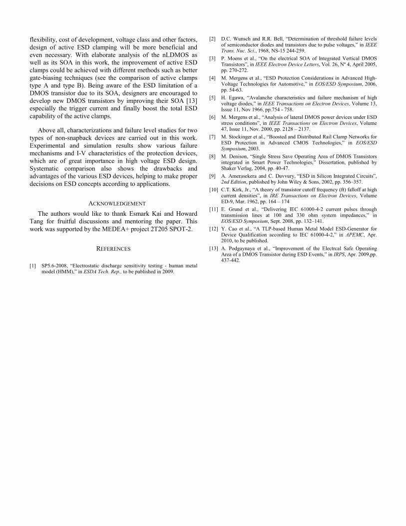
B. Failure levels study on actively controlled and single nLDMOS In order to study the failure levels of active structures, TLP
tests with various pulse durations were applied to the active ESD devices. Figure 8 gives the performance of a type B device employing a smaller nLDMOS as in Figure 7. Vf-TLP measurements in TDRs setup were used for 5ns pulse width tests. Apart from the pn-diodes, as pulse widths were scaled
down below 20ns the snapback points start crowding together with less deviation of Vf and If. In other words, with less energy content of the TLP pulses, failure power levels of the active structure do not increase significantly. Note that some other active devices including type A and type B on different breakdown voltages are also characterized with TLP and vf-TLP, showing the same effect.
As already discussed, ESD capability of proper designed active clamping structures relies on the bigFET, in this case the nLDMOS transistor. To understand the phenomenon of less increasing of failure power at short pulse durations, electrical SOA of the nLDMOS is investigated applying stresses with various pulse durations instead of the standard TLP with 100ns pulse width. Two groups of measurements were performed for different Vgs as depicted in Figure 9. Note that for tests with 2.5ns and 5ns pulse durations, the failure points forming pure electrical SOA remain nearly unchanged. This can be used to explain the fact that failure power of active ESD structures is
saturated as pulse duration getting shorter. It is worth to mention that the SOA measurements were repeated also with different rise-times (100ps and 1ns), delivering the same phenomenon. No significant difference regarding rise-times was observed. This implies the triggering of snapback has no significant dependence on dV/dt or dI/dt.
In the active clamping structures, the gate voltage of nLDMOS should be biased on a relative high level to facilitate a higher failure current. This encourages the further analysis of the used nLDMOS under high voltage gate-biasing with 2-D TCAD simulation involved. As marked in Figure 9, A to D represents four regions which are of concern for ESD designers:
• Region A: nLDMOS works in saturation region as a usual MOSFET, where the channel is pinched off with total electron current flowing through the
30 40 50 60−2
0
2
4
6
8
10
12
14
TLP Voltage (V)
TLP
Cur
rent
(A)
5ns10ns20ns50ns100ns200ns500ns1500ns
Figure 8: TLP I-V characteristic of a 25V voltage class active clamping structure named e25 type B tested with various pulse widths from 5ns to 1500ns. The crowding of failure points tested with below 20ns long pulses is indicated comparing to the case of the pn-diode in Figure 1.
source
p-body
gate drain
n-epi
STIchannel
(a) (b)
n+
Figure 10: Simulation of (a) electron current density and (b) hole current density in region A. Source and body contacts were shorted to ground whilethe gate was biased on 10V. The same simulation setup was also applied to Figure 11 to Figure 13.
(a) (b)
A A’
Figure 11: Simulation of (a) hole current density and (b) impact ionization amplitude in region B. Significant hole current starts flowing to the body contact in comparison with region A (Figure 10 (b)). The delocalization of the impact ionization maximums as well as electric field peaks along the cut line AA’ represents Kirk effect.
Figure 9: Electrical SOA of nLDMOS for Vgs=10V and 16V with different pulse durations. Pulses shorter than 20ns no longer enhance the SOA significantly. A to D indicates four different regions of I-V characteristics where the transistor gate is biased with high voltage.
narrow channel to the drain contact. No additional hole current through n-epi layer and p-body region to the body contact can be observed (Figure 10).
• Region B: In this region, avalanche multiplication occurs accompanied with strong local electric field [8] [9]. The electrons generated due to impact ionization flow to drain contact while the holes flow to the body, providing a significant addition on total current (Figure 11). The delocalization of the electric field peaks under high current density to the more highly doped drain region is called Kirk effect [10] after its first investigator in bipolar transistors, having a similar effect as so called Egawa effect in pn-diodes described earlier.
• Region C: As the generation of the holes keeps increasing, additional local maximums of impact ionization can be observed at p-body to n-epi junction area (Figure 12), exhibiting the main difference of region C and B. Note that no significant electron current flows from source through p-body to drain as the parasitic bipolar transistor is not triggered yet.
• Region D: This region is defined at the moment when snapback just happens. As hole current through p-body is sufficient large to build up an ohmic voltage drop on base-emitter junction, which is larger than the build-in voltage. The bipolar transistor is then triggered accompanied with significant electrons injected into p-body and holes into source (Figure 13).
In addition to the simulation results comparing the electric parameters in four regions inside the transistor, transient simulation using the commercial SDEVICE simulator by SYNOPSYS was also performed for the used nLDMOS in electro-thermal mode.
Figure 14 depicts the waveforms of voltage and maximal lattice temperature of the LDMOS with Vgs of 10V under various drain-source current biasing. X1 to X5 denotes the time instants when the triggering of the npn-transistor takes place. These specific time points were extracted by examining the electron current density in the device cross section (Figure 13 (a)). A time instant was then recorded, when a large amount of electrons are not only found in the MOS channel but also in the p-body region. This means the device was driven into the critical region D. In the measurements, triggering of the parasitic bipolar transistor is accompanied immediately with voltage snapback due to current filamentation (Figure 9). In the simulation however, the voltage snapback of an ideal homogenous device occurs after a certain time period (tens of nanoseconds shown in Figure 14) beyond the bipolar triggering. The simulated maximal voltage peaks observed in the transient waveforms are therefore not usable to identify the snapback or device failure in practice. With X1 to X5 as the
(a) (b)
injection of holes
npn
Figure 13: Simulation of (a) electron current density and (b) hole current density in region D. Comparing to the operation as MOSFET in Figure 10 (a), the npn bipolar transistor is now dominating the nLDMOS behavior leading to snapback.
(a) (b)
A A’
MOS
Figure 12: Simulation of (a) electron current density and (b) impact ionization amplitude in region C. Electron current is distributed similar as in region A. Along the cut line AA’, three local maximums of impact ionization can be observed.
100 101 102 103
102
Time (ns)
Pow
er to
Fai
lure
(mW
)
12
3
4
5
Figure 15: Simulated power to failure (triggering of the bipolar transistor) of the nLDMOS at Vgs=10V. X1 to X5 indicates the same failure points shown in Figure 14.
0
20
40
60
80
500
1000
1500
1E-10 1E-9 1E-8 1E-7 1E-6
Time (s)
1E-11
Dra
in S
ourc
e Vo
ltage
(V) M
aximal Tem
perature (K)
Vds, I = 1.3mAVds, I = 1.1mAVds, I = 1.0mAVds, I = 0.8mA Vds, I = 0.6mATmax, I = 1.3mATmax, I = 0.6mA
12 3
4
5
Figure 14: Transient simulation of drain-source voltage corresponding to various drain-source current pulses with rise-time of 1ns. In case current reaches a critical level, snapback takes place at very beginning of the pulse (indicated by X1), where the self-heating of the nLDMOS is not significant.
failure points of the studied nLDMOS, power failure levels can be plotted in Figure 15. Note that the same effect comes out as described in the investigation of SOA (Figure 9). Again, power to failure of nLDMOS as well as the active ESD protection structures using nLDMOS as the bigFET cannot increase significantly by shortening the pulse width. Furthermore, a dynamic triggering of the inherent bipolar transistor due to dV/dt or dI/dt is not observed in the device simulation as well.
IV. COMPARISON OF FAILURE LEVELS AND DISCUSSION As the major failure mechanisms of two types of non-
snapback ESD devices are already detailed discussed in the former sections, systematic comparison of the protection devices is performed in order to achieve a better overview.
Figure 16 compares the failure power levels per unit area of the investigated non-snapback ESD devices calculated with If·Vf /area. Very good scalability is found in the pn-diodes while certain dependences on trigger types are seen in the active ones due to gate-biasing issues. For short pulse durations, the curves of failure power of active circuits become flat confirming the phenomenon simulated for nLDMOS in Figure 15.
Robust junction of pn-diodes enables higher power to failure levels due to the fact that the heat generated mainly in junction area can be dissipated into all directions inside the device, where the hotspots within a DMOS based active clamping structure are located in the surface area. Besides, the inherent bipolar snapback and accompanying current filamentation are the major constraint of the active devices in the short pulse range. In contrast to this, ruggedness of pn-diodes is only limited thermally rather than electrically.
However, as emphasized earlier, absolute maximum value of current conducting capability or power/energy to failure
might not be the right measure of evaluating the area efficiency of ESD devices. ESD window or the maximum allowed voltage (Vmax) defined by the protected IC circuitries should be considered in each ESD design. The ESD window could be enlarged by e.g. employing a secondary protection concept using serial on-chip resistance with extra area cost. But this is often not possible in the real applications. Therefore, effective Ron provides a better comparison of the area efficiency
regarding ESD. Figure 17 illustrates effective Ron over pulse duration of several devices with Vmax assumed with 80V. Note that Ron area product of active structures does not change with higher breakdown voltage compared to the pn-diodes (Figure 3). In 45V voltage class, e45 type B is already leading in terms of area efficiency with lower effective Ron for pulse duration larger than 50ns. The benefit of a proper active clamping design could be even higher when an ESD device with higher Vbd is required.
In addition to the effective Ron as discussed above, several other advantages of active clamping structures or drawbacks of pn-diodes are summarized as following:
• Zener triggered active clamping structures give the possibility of defining Vbd in a more flexible way where pn-diode demands process design which is much more time consuming to generate a new device with another breakdown voltage.
• For higher breakdown voltages needed in certain applications, pn-diodes are only realizable on extra cost of area efficiency.
• Process fluctuation and temperature dependence of pn-diode is usually much higher than the existing Zener diode and nLDMOS in the active structures.
100 101 102 103 104100
101
102
103
Pulse Duration (ns)
Pow
er to
Fai
lure
per
Are
a (k
W/m
m2 )
pn-diodes
active clamping structures
flat line region
s9e25k1s9e25k2s9e25k3s9e25k4s9e45k1s9e45k2s9e45k3s9e45k4e25 Type Ae25 Type Be45 Type B
Figure 16: Failure power levels per unit area of various non-snapback devices with different dimensions and Vbd. Pn-diodes show overall advantage in terms of the current capability per unit area.
100 101 102 10310-2
10-1
100
Pulse Duration (ns)
s9e25k1 Vmax=80Vs9e45k1 Vmax=80Ve25 Type Be45 Type B
Effe
ctiv
e R
on @
ES
D •
Are
a (Ω
• m
m )2
Figure 17: Effective Ron area product with Vmax=80V. 80V is already an optimistic value in HV ESD design windows of 25V, 45V or 55V voltage classes. For short pulse durations, pn-diodes still have more area efficiency.
Among the device comparison and characterization, behavior of these two types of ESD devices under realistic ESD pulses needs to be studied further. In order to address the impact of different failure mechanisms for non-snapback devices in a practical manner, a novel human metal model (HMM) tester based on coaxial line technique [11] is used as the ESD test method which can deliver the same shape of current pulse defined in system-level ESD and provide a excellent resolution of transient voltage and current measurements [12].
Figure 18 and Figure 19 show the waveforms confirming that the decisive damage due to snapback actually comes from the initial peak of ESD pulses for active structures, while the pn-diode burned out by certain energy content of the broad peak. For the active device, the calculated first peak power per unit area is located on the flat line region shown in Figure 16. On the other hand, the pn-diode is not damaged by the first peak because the peak power is below the power to failure level at the corresponding pulse duration.
Again, applying system-level ESD pulse on the single ESD devices delivers the characterizations but does not reflect the real ESD protection capabilities. For example, a circuit protected with the tested pn-diode would probably not survive a 6kV GUN discharge since the clamping voltage of the diode exceeds 110V, which is already beyond the ESD window. Nevertheless, from the effective Ron point of view, the first peak of the HMM pulse in the range of several nanoseconds and the broad peak in the range of tens of nanoseconds both imply the fact that the pn-diode could be in favor in common system-level ESD applications compared to the active ESD protection in 25V voltage class as exhibited in Figure 17.
V. CONCLUSIONS Conventional avalanche pn-diodes with designed
breakdown voltage for HV ESD utilize robust vertical junction deep inside the silicon and deliver inherently very good ESD ruggedness with high area efficiency. Egawa effect occurs above certain current density, providing an extra advantage of using pn-diodes. Characteristics of active ESD structures rely mainly on the used bigFET, in this case, the nLDMOS. The saturation effect of failure power levels while shortening the pulse length is studied carefully both from test and simulation results.
In this work, a novel aspect of evaluating non-snapback ESD devices in a wide range of pulse duration is presented based on Wunsch-Bell theory. However, Wunsch theory has its limitation in practical use because of the simplified thermal models. Additionally, ESD hardness of active ESD protections is not able to be estimated using Wunsch theory. In short-pulse range, active devices actually suffer from electrical failure rather than a thermal one. The slope 0.5 is thus no longer applicable according to Figure 16. For the evaluation of ESD efficiency considering ESD window, Figure 17 provides the possibility of choosing ESD devices properly against ESD pulses depending on their pulse lengths. HMM tests with system-level ESD like pulse waveforms were performed on the pn-diode and the active device as an example. It was shown the pn-diode in 25V voltage class is more efficient according to the effective Ron in the first peak and the broad peak ranges.
Generally, the much lower area efficiency of nLDMOS in short-pulse region implies that pn-diodes furnish a better approach for protecting ESD pulses with a short-pulse part such as IEC 61000-4-2, HMM, CDE and etc. Active ESD devices would be of less interest in these cases since the dangerous bipolar triggering can be launched by a critical power level, resulting in overall sensitivity of active clamps on peak power. More detailed, on a certain voltage level across drain-source of nLDMOS, the current density in the body region will reach a sufficient value to trigger the parasitic bipolar transistor, driving the MOS transistor into destructive snapback mode. On the other hand however, within the given ESD window, active clamping structures become eventually more area efficient compared to pn-diodes. Active ESD solution is hence a very attractive alternative for ESD design against pulses such as HBM. Furthermore, if one considers
−40 −20 0 20 40 60 80 100 120 140 160−20
0
20
40
60
80
100
120
Vol
tage
(V)
Time (ns)
−5
0
5
10
15
20
25
30
Current (A
)
voltage: stress causing failurevoltage: last stress before failurecurrent: last stress before failure
thermal failure
Figure 19: Pn-diode s9e25k2 tested with HMM. Thermal failure observed in the broad peak region. This device alone can sustain a 6kV system-level ESD discharge (150pF/330Ω).
-40 -20 0 20 40 60 80 100 120 140 160-10
0
10
20
30
40
50
60
70
Vol
tage
(V)
Time (ns)-40 -20 0 20 40 60 80 100 120 140 160
-2
0
2
4
6
8
10
12
14
Current (A
)
voltage: stress causing failurevoltage: last stress before failurecurrent: last stress before failure
snapback after the first peak
Figure 18: Active device e25 type B tested with HMM. Snapback observed right after the initial peak causing damage of the device. This device alone can sustain a 3.5kV system-level ESD discharge (150pF/330Ω).
flexibility, cost of development, voltage class and other factors, design of active ESD clamping will be more beneficial and even necessary. With elaborate analysis of the nLDMOS as well as its SOA in this work, the improvement of active ESD clamps could be achieved with different methods such as better gate-biasing techniques (see the comparison of active clamps type A and type B). Being aware of the ESD limitation of a DMOS transistor due to its SOA, designers are encouraged to develop new DMOS transistors by improving their SOA [13] especially the trigger current and finally boost the total ESD capability of the active clamps.
Above all, characterizations and failure level studies for two types of non-snapback devices are carried out in this work. Experimental and simulation results show various failure mechanisms and I-V characteristics of the protection devices, which are of great importance in high voltage ESD design. Systematic comparison also shows the drawbacks and advantages of the various ESD devices, helping to make proper decisions on ESD concepts according to applications.
ACKNOWLEDGEMENT The authors would like to thank Esmark Kai and Howard
Tang for fruitful discussions and mentoring the paper. This work was supported by the MEDEA+ project 2T205 SPOT-2.
REFERENCES
[1] SP5.6-2008, “Electrostatic discharge sensitivity testing - human metal model (HMM),” in ESDA Tech. Rep., to be published in 2009.
[2] D.C. Wunsch and R.R. Bell, “Determination of threshold failure levels of semiconductor diodes and transistors due to pulse voltages,” in IEEE Trans. Nuc. Sci., 1968, NS-15 244-259.
[3] P. Moens et al., “On the electrical SOA of Integrated Vertical DMOS Transistors”, in IEEE Electron Device Letters, Vol. 26, Nº 4, April 2005, pp. 270-272.
[4] M. Mergens et al., “ESD Protection Considerations in Advanced High-Voltage Technologies for Automotive,” in EOS/ESD Symposium, 2006, pp. 54-63.
[5] H. Egawa, “Avalanche characteristics and failure mechanism of high voltage diodes,” in IEEE Transactions on Electron Devices, Volume 13, Issue 11, Nov 1966, pp.754 - 758.
[6] M. Mergens et al., “Analysis of lateral DMOS power devices under ESD stress conditions”, in IEEE Transactions on Electron Devices, Volume 47, Issue 11, Nov. 2000, pp. 2128 – 2137.
[7] M. Stockinger et al., “Boosted and Distributed Rail Clamp Networks for ESD Protection in Advanced CMOS Technologies,” in EOS/ESD Symposium, 2003.
[8] M. Denison, “Single Stress Save Operating Area of DMOS Transistors integrated in Smart Power Technologies,” Dissertation, published by Shaker Verlag, 2004, pp. 40-47.
[9] A. Amerasekera and C. Duvvury, “ESD in Silicon Integrated Circuits”, 2nd Edition, published by John Wiley & Sons, 2002, pp. 356–357.
[10] C.T. Kirk, Jr., “A theory of transistor cutoff frequency (ft) falloff at high current densities”, in IRE Transactions on Electron Devices, Volume ED-9, Mar. 1962, pp. 164 – 174
[11] E. Grund et al., “Delivering IEC 61000-4-2 current pulses through transmission lines at 100 and 330 ohm system impedances,” in EOS/ESD Symposium, Sept. 2008, pp. 132–141.
[12] Y. Cao et al., “A TLP-based Human Metal Model ESD-Generator for Device Qualification according to IEC 61000-4-2,” in APEMC, Apr. 2010, to be published.
[13] A. Podgaynaya et al., “Improvement of the Electrcal Safe Operating Area of a DMOS Transistor during ESD Events,” in IRPS, Apr. 2009,pp. 437-442.