0885-8993 (c) 2016 IEEE. Personal use is permitted, but republication/redistribution requires IEEE permission. See http://www.ieee.org/publications_standards/publications/rights/index.html for more information. This article has been accepted for publication in a future issue of this journal, but has not been fully edited. Content may change prior to final publication. Citation information: DOI 10.1109/TPEL.2016.2643006, IEEE Transactions on Power Electronics TPEL-REG-2016-08-1512 1 Abstract— This paper presents an isolated LLC series resonant DC/DC converter with novel frequency adaptive phase shift modulation control, which suitable for wide input voltage (200-400V) applications. The proposed topology integrates two half-bridge in series on the primary side to reduce the switching stress to half of the input voltage. Unlike the conventional converter, this control strategy increases the voltage gain range with ZVS to all switches under all operating voltage and load variations. Adaptive frequency control is used to secure ZVS in the primary bridge with regards to load change. To do so, the voltage gain becomes independent of the loaded quality factor. In addition, the phase shift control is used to regulate the output voltage as constant under all possible inputs. The control of these two variables also significantly minimizes the circulating current, especially from the low voltage side, which increases the efficiency as compared to a conventional converter. Experimental results of a 1Kw prototype converter with 200-400V input and 48V output are presented to verify all theoretical analysis and characteristics. Index Terms— LLC, resonant converter, frequency adaptive phase shift modulation control (FAPSM), Zero- Voltage-Switching (ZVS), wide gain range. I. INTRODUCTION HE renewable-energy sources, such as photovoltaic, wind power and fuel cell system are highly promising sources to mitigate the power-generation crisis throughout the world. Power converters have become the essential part of generation systems to utilize the fluctuating renewable energy. The power converter which is capable of generating constant output with variable input is the most effective ones for the renewable power generation systems. It is also common to use a bi-directional converter to interface with energy storage systems. Manuscript received August 4, 2016; revised November 10, 2016 accepted December 11, 2016. Date of publication XX, XXXX; Date of current version XX, XXXX. This work was supported by the High Impact Research of University of Malaya−Ministry of higher education of Malaysia under Project UM.C/625/1/HIR/MOHE/ENG/17 and Postgraduate Research Grant (PPP) Project No. PG269-2016A. Recommended for publication by Associate Editor XXXX. The authors are with the Power Electronics and Renewable Energy Research Laboratory, Department of Electrical Engineering, University of Malaya, Kuala Lumpur 50603, Malaysia (e-mail: [email protected], corresponding e-mail: [email protected]) Dual active bridge (DAB) has drawn lots of interest in the energy storage systems due to having the bi-directional capability with high-efficiency, high-power density, and reliability [1]-[7]. The voltage gain of DAB is limited to unity to maintain ZVS for all load variations [8], [ 9]. It also suffers from high circulating current in the secondary side and high turn-off losses. In order to extend the gain range with ZVS or minimize the circulating energy further, some control strategies were proposed in [1], [3], [10]-[13]. However, these control strategies cannot overcome all the disadvantages at a time. The resonant version of DAB is called DAB resonance converter (DABRC) has the same performance with improved efficiency [14]-[21]. In [16] a dual-full bridge series resonance converter with fixed frequency phase shift control has been proposed and analyzed using modified fundamental harmonic approximation approach. The voltage gain of this converter has to be limited to unity to maintain the ZVS over the wide load range, and the circulating current in the low-voltage side is high as well. As a result, the efficiency is degraded, especially when the voltage gain deviates from the unity. Therefore, the converter becomes unsuitable for wide input voltage applications. A bi-directional DAB LLC converter for energy storage systems has been proposed in [17]. This converter operated at a constant frequency, but the duty ratio is different based on desired voltage gain. An extra inductor is added to make the topology symmetrical in any operating modes, which increases the power loss and cost for the system. The gain is still limited to maintain high conversion efficiency. It is also operated in the capacitive slope region which is suitable for ZCS realization. The topology in [22], is an integration of a half bridge (HB) and full bridge (FB) LLC circuit. A simple PWM control technique with more switches has been used for wide input voltage applications. It can be used only for unidirectional power flow. For the certain input voltage, the time interval of the resonant current being equal to the magnetizing current is longer, which increased the conduction loss as well as hinders the improvement of efficiency. Several attempts have taken to increase the input voltage range in the literature. Three-level DC/DC converters have been introduced to minimize the voltage stress across switches. They have been used to increase high-power density, operating over wide input voltage range and best suitable for high-voltage applications [23]-[25]. But all the converters related to unidirectional dc-dc applications. The three-level bidirectional LLC resonant converter has been proposed in [18], where the voltage stress across switches depends on voltage gain, and ZVS appeared only in the primary switches. A Frequency Adaptive Phase Shift Modulation Control Based LLC Series Resonant Converter for Wide Input Voltage Applications S M Showybul Islam Shakib and Saad Mekhilef, Senior Member, IEEE T
Transcript
0885-8993 (c) 2016 IEEE. Personal use is permitted, but republication/redistribution requires IEEE permission. See http://www.ieee.org/publications_standards/publications/rights/index.html for more information.
This article has been accepted for publication in a future issue of this journal, but has not been fully edited. Content may change prior to final publication. Citation information: DOI 10.1109/TPEL.2016.2643006, IEEETransactions on Power Electronics
TPEL-REG-2016-08-1512
1
Abstract— This paper presents an isolated LLC series
resonant DC/DC converter with novel frequency adaptive
phase shift modulation control, which suitable for wide
input voltage (200-400V) applications. The proposed
topology integrates two half-bridge in series on the
primary side to reduce the switching stress to half of the
input voltage. Unlike the conventional converter, this
control strategy increases the voltage gain range with ZVS
to all switches under all operating voltage and load
variations. Adaptive frequency control is used to secure
ZVS in the primary bridge with regards to load change. To
do so, the voltage gain becomes independent of the loaded
quality factor. In addition, the phase shift control is used
to regulate the output voltage as constant under all
possible inputs. The control of these two variables also
significantly minimizes the circulating current, especially
from the low voltage side, which increases the efficiency as
compared to a conventional converter. Experimental
results of a 1Kw prototype converter with 200-400V input
and 48V output are presented to verify all theoretical
analysis and characteristics.
Index Terms— LLC, resonant converter, frequency
adaptive phase shift modulation control (FAPSM), Zero-
Voltage-Switching (ZVS), wide gain range.
I. INTRODUCTION
HE renewable-energy sources, such as photovoltaic, wind
power and fuel cell system are highly promising sources
to mitigate the power-generation crisis throughout the
world. Power converters have become the essential part of
generation systems to utilize the fluctuating renewable energy.
The power converter which is capable of generating constant
output with variable input is the most effective ones for the
renewable power generation systems. It is also common to
use a bi-directional converter to interface with energy storage
systems.
Manuscript received August 4, 2016; revised November 10, 2016 accepted
December 11, 2016. Date of publication XX, XXXX; Date of current version XX, XXXX. This work was supported by the High Impact Research of
University of Malaya−Ministry of higher education of Malaysia under Project
UM.C/625/1/HIR/MOHE/ENG/17 and Postgraduate Research Grant (PPP) Project No. PG269-2016A. Recommended for publication by Associate Editor
XXXX.
The authors are with the Power Electronics and Renewable Energy
Research Laboratory, Department of Electrical Engineering, University of
0885-8993 (c) 2016 IEEE. Personal use is permitted, but republication/redistribution requires IEEE permission. See http://www.ieee.org/publications_standards/publications/rights/index.html for more information.
This article has been accepted for publication in a future issue of this journal, but has not been fully edited. Content may change prior to final publication. Citation information: DOI 10.1109/TPEL.2016.2643006, IEEETransactions on Power Electronics
TPEL-REG-2016-08-1512
2
In this topology, they used an extra flying capacitor and
auxiliary switches, which make the converter operation
complex and increased the cost of the system.
The major contribution of this paper is to propose a modified
complete soft switched LLC resonant converter with a simple
FAPSM control for a wide voltage gain range applications.
This topology is composed of two half bridge (HB) connected
in series but sharing the same resonance tank and high-
frequency transformer. The series combination of four
switches reduces the voltage stress across each switch equal to
half of the input voltage. It also used active rectifier in the
secondary side of the transformer and becomes the key
component of an energy storage system (ESS) [16] to enable
the bi-directional power flow. The control proposed for this
circuit based upon two control variables such as: switching
frequency and phase shift angle of the secondary switches.
The Switching frequency changes with load in such a way
that, it is secured ZVS in the primary side for all phase shift
angles. Automatically, it maintains the converter gain
characteristics identical regardless of load conditions over all
phase shift angles. As a result, the proposed converter can be
capable of operating at wide gain range with ZVS under all
load conditions. On the other hand, the phase shift changes
according to input variations only. It can be regulated the
output voltage tightly and remains constant under all input
voltages. This control overcomes the unity gain problem of
conventional DAB LLC resonant converters. It makes the
converter voltage gain is independent of the quality factor Q.
Unlike the conventional DAB LLC resonant converter [16],
the proposed control increases the gain range and makes the
converter best suitable for renewable-energy generation
system. In addition, the simultaneous use of two variables also
reduces the circulating current (or reactive power) from the
secondary bridge, especially at light load conditions.
Furthermore, proper design of the inductor ratio (which has no
effects on voltage gain), reduces the conduction losses as well
as increases the efficiency of the converter.
II. CONVERTER TOPOLOGY AND OPERATING PRINCIPLE
Fig. 1. Proposed LLC resonant converter.
The proposed LLC resonant DC/DC converter with the
active rectifier for the high and wide input voltage applications
is shown in Fig. 1. The switches in both sides are connected in
series with an LLC resonant tank and a high-frequency
transformer. An extra inductor is used with transformer
leakage inductor to get desired circuit operation. The series
resonance capacitor Cr absorbs the DC component from the
inverted signal which hinders the transformer saturation. The
input series capacitors C1 and C2 have the same capacitance
value, and they used to clamp the primary switch voltage
stress to half of the input voltage. The value of output
capacitor Co should be chosen high enough to keep the output
voltage free from ripple. The transformer has to be designed in
such a way, which keeps the Lm as high as possible to reduce
the conduction losses from the system.
Fig. 2. shows the steady-state waveforms of a proposed
converter where all the switches in both primary and
secondary side have the constant duty cycle of 0.5.The outer
pair of a primary switches S1 and S4 share the same gate
signals, while the inner pair of switches S2 and S3 turns on and
off simultaneously. The secondary active rectifier switches Sa
and Sb also turns on and off with a constant duty cycle of
0.5.The switching frequency always remains higher than the
resonant frequency, thus, the converter operated in the
negative slope region.
Fig. 2. Key operating waveforms of LLC resonant converter.
The phase-shift angle ψ between primary and secondary
switches is used to control the power flow and output voltage
regulation. If the phase-shift angle is greater than zero i.e. ψ >
0, power flows from the primary side to the secondary side,
otherwise (i.e ψ < 0) power flows in the reverse direction. The
operation of a proposed converter topology is symmetrical for
both forward and backward power flow. So only the forward
power flow has been analyzed in this paper. The operation
modes of proposed DC/DC LLC resonant converter for each
switching cycle are divided into the 16 stages. Only t0-t8 is
introduced and explained due to the symmetrical nature of
every half switching cycle. The corresponding equivalent
circuits for half switching cycle are depicted in Fig. 3.
Stage: 1 [to – t1 ] : In the beginning of this interval (t= t0), the
gate signals across S2 and S3 are being removed. Then, the
lossless snubbing capacitors Cs2 and Cs3 start charging by the
resonance current Ir. Accordingly, the voltages Vs2 and Vs3
across S2 and S3 rise gradually from zero to half of the input
voltage. On the other hand, the voltages Vs1 and Vs4 across S1
and S4 decrease rapidly from Vin/2 to zero by discharging of
Cs1 and Cs4. In this interval, S2 and S3 turn off with ZVS
transition and the voltage across the resonant tank rises
gradually to the Vin. This interval lasts until the snubbing
Gat
e S
ignal
s
0885-8993 (c) 2016 IEEE. Personal use is permitted, but republication/redistribution requires IEEE permission. See http://www.ieee.org/publications_standards/publications/rights/index.html for more information.
This article has been accepted for publication in a future issue of this journal, but has not been fully edited. Content may change prior to final publication. Citation information: DOI 10.1109/TPEL.2016.2643006, IEEETransactions on Power Electronics
TPEL-REG-2016-08-1512
3
capacitors in the primary side switches charged and
discharged fully.
Stage: 2 [t1 - t2]: This interval starts when Vs1 and Vs4 are
forced to be zero at t= t1 ; then, their antiparallel diodes D1
and D4 become in forward biased. Thus, tank power is
pumped back into the primary side with a negative resonant
current flowing through D1 and D4 while the secondary current
still flows into the load through Da. Stage-2 completes as the
gating signals of the switch S1 and S4 are given.
Stage: 3 [t2 - t3]: The signals for S1 and S4 are triggered,
while D1 and D4 are still conducting. The current It and I2
become zero at the end of this interval. Furthermore, the
resonant current flows towards zero; consequently, ZVZCS
(Zero voltage and Zero current switching) turn on can be
achieved in S1 and S4.
Stage: 4 [t3 - t4]: At, t3, It reaches zero and starts increasing
towards positive value while the secondary current flows in
reverse direction through Sa. Reactive power (or, reverse
power) persists throughout this interval, which increases the
conduction losses. This stage ends when the Sa is turned off.
Stage: 5 [t4- t5]: In the beginning of this stage, the secondary
current again flows in positive direction towards the load. The
capacitors across Sa and Sb are charging and discharging
gradually during this interval. Thus, ZVS turn off can be
achieved in the secondary switch Sa. The reflected voltage
across the transformer primary side is switched to a positive
value, which increases the magnetizing current (ILm) linearly
towards a positive direction.
Stage: 6 [t5 – t6]: This interval begins when Vsb is forced to
be zero at t5; then the antiparallel diode Db becomes in forward
biased. This interval ends when the gate signal is applied
across the switch Sb.
Stage: 7 and Stage: 8 [t6- t8]: In this interval switch, Sb turns
on with ZVZCS. The resonant current Ir goes towards zero and
shifts from diodes to corresponding switches. After the
moment, the power is transferred from the primary side to the
secondary side through the resonant tank. This interval
completes when S1 and S4 are turned off.
III. STEADY STATE ANALYSIS
The power is transferred from input to the load with the aid
of resonant tank components, Cr, Lr, and Lm. Hence, the
current in the resonant tank nearly sinusoidal as shown in Fig.
2.This allows the use of fundamental harmonic approximation
(FHA) to analyze the DC characteristic of the converter,
which considers that only the fundamental component of the
square wave is responsible for transferring the power to the
load. Based on the FHA, the ac-equivalent two-port model is
derived as shown in Fig. 4. All the inductors, capacitors,
diodes, switches and the high-frequency transformer are
assumed to be ideal in the model. The parameters which are
transferred to the primary side are denoted by superscript (‘/’).
The following parameters are normalized for the resonance
converter:
Vbase = 𝑉𝑖𝑛
2 , Zbase = √
Lr
Cr = ωrLr =
1
ωrCr
ωbase= ωr = 1
√LrCr ; Ibase =
Vbase
Zbase (1)
where, ωr is the angular series resonance frequency.
Stage: 1
Stage: 2
Stage: 3
Stage: 4
Stage: 5
Stage: 6
Stage: 7
Stage: 8
Fig. 3. Equivalent circuits for different time intervals in half
of the switching cycle for the forward power flow.
The normalized switching frequency can be defined as
F = ωs
ωr (2)
Where, ωs = 2πfs and fs is the switching frequency.
Vr1.N
-jXcr.N jXLr.N
jXLm.N
1:1It1.N
Vt1.N
+
-
Z/ac.N
Ir1.N
ILm1.N
Fig. 4. AC-equivalent circuit of LLC resonant converter.
0885-8993 (c) 2016 IEEE. Personal use is permitted, but republication/redistribution requires IEEE permission. See http://www.ieee.org/publications_standards/publications/rights/index.html for more information.
This article has been accepted for publication in a future issue of this journal, but has not been fully edited. Content may change prior to final publication. Citation information: DOI 10.1109/TPEL.2016.2643006, IEEETransactions on Power Electronics
TPEL-REG-2016-08-1512
4
The normalized reactances of the resonance tank can be
expressed as
XLr.N = F ; XCr.N = 1
F; XLm.N =
F
K (3)
where, K = Lr
Lm is defined as inductance ratio.
The current in the secondary side is always in continuous
conduction mode in the proposed topology. There is phase
difference ϴ, between the transformer secondary voltage and
current as shown in Fig. 2. Thus the circuit, including HF
transformer, active rectifier, output filter and load can be
represented by equivalent impedance ‘𝑍𝑎𝑐.𝑁/
’.
𝑍𝑎𝑐.𝑁/
= cos ϴ
Q
< (− ϴ) (4)
Where ϴ = (ψ – β) is the phase angle of the Zac.N/
and Q is the
quality factor which can be expressed as follows
Q = π2ZBPo
8n2Vo2 (5)
The relationship between the phase angle ϴ, controllable
phase shift ψ and switching frequency can be calculated from
the AC impedance network given in Fig. 4.
ϴ = tan−1(FK+F−K
F⁄
Q(F2−1)− cotψ) (6)
The input impedance of the two-port network shown in Fig. 4
can be calculated as follows:
Zin.N = ⎹ Zin.N ⎹ < Ф
where, Ф = tan−1[(F −1
F) (
K2
QF2 − 2K tan ϴ
F+
Q
cos2 ϴ) +
K
FQ−
tan ϴ] (7)
It can also be calculated the phase angle β in between Vr1.N and
It1.N as follows:
β = tan−1(Q(F2−1) csc2ψ
k(F + FK ⁄ − 1 F⁄ )
− cotψ) (8)
A. Converter Gain
From the equivalent circuit in Fig. 4, the voltage gain can be
written as follows:
Voltage gain , G = ⎹𝑉𝑡1.𝑁
𝑉𝑟1.𝑁⎹ (9)
The voltage gain is simplified as follows
G = 1
√{(1+𝐾−𝑘𝐹2⁄ )−[
𝑄(𝐹2−1)
𝐹∗(
𝐹𝐾+𝐹−𝐾𝐹⁄
𝑄(𝐹2−1)−cotψ)]}
2
+{𝑄(𝐹2−1)
𝐹}2 (10)
It is seen that, when ϴ = 0, the operation of the proposed LLC
resonant converter is the same as a conventional LLC resonant
converter with diode rectifier and equivalent load can be seen
as a resistor [26], [27]. These two voltage gains are drawn in
Fig. 5.
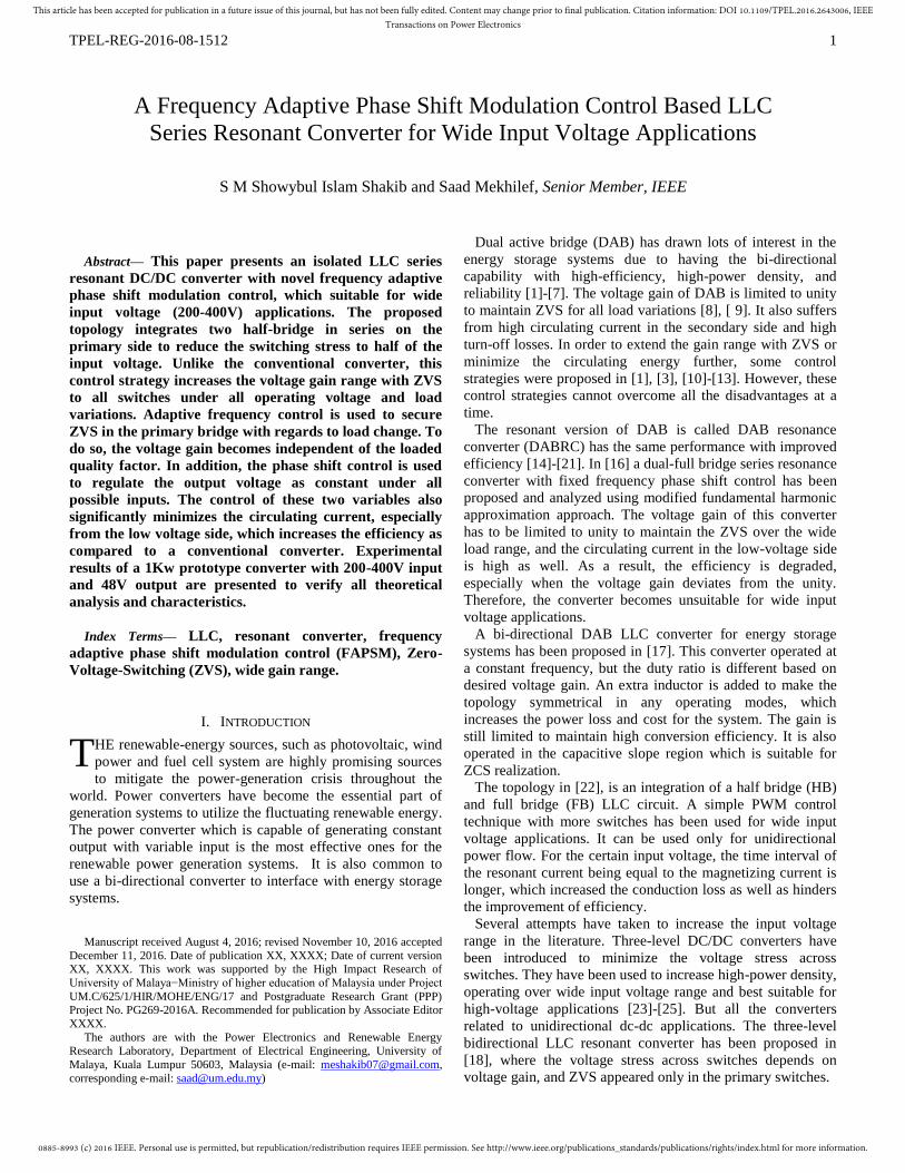
Fig. 5. Plots of voltage gain with regards to normalized
switching frequency at K=0.2, Q=2.5.
It is observed that the voltage gain of conventional LLC
converter always remains under unity in the negative slope
region at high Q values like 2.5. On the other hand, the gain of
the proposed converter can be varied widely in the negative
slope region even at high-quality factor. Thus, the proposed
converter can be operated at wide input voltages from no load
to full load.
B. Reverse Power
The reverse energy exists for the phase difference between
transformer voltage and current, which means; conduction
losses will be increased due to the part of the energy is
transferred back and forth between output and input side. It
will be high at minimum input voltage condition. The
minimum input voltage has to be limited due to a large amount
of reactive power in the system. To simplify the calculation,
the reverse energy per unit time can be represented by the
reactive power. The ratio of reverse power to the output power
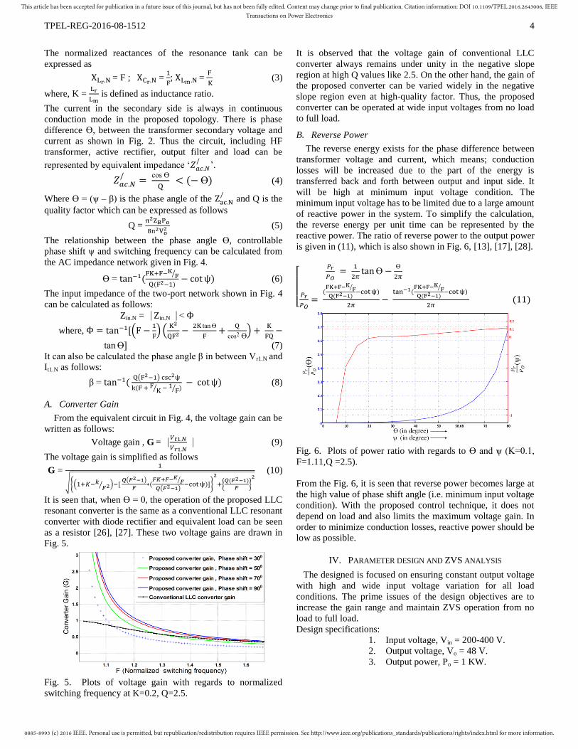
is given in (11), which is also shown in Fig. 6, [13], [17], [28].
[
𝑃𝑟
𝑃𝑂 =
1
2𝜋tan ϴ −
ϴ
2𝜋
𝑃𝑟
𝑃𝑂=
(FK+F−K
F⁄
Q(F2−1)−cotψ)
2𝜋−
tan−1(FK+F−K
F⁄
Q(F2−1)−cotψ)
2𝜋 (11)
Fig. 6. Plots of power ratio with regards to ϴ and ψ (K=0.1,
F=1.11,Q =2.5).
From the Fig. 6, it is seen that reverse power becomes large at
the high value of phase shift angle (i.e. minimum input voltage
condition). With the proposed control technique, it does not
depend on load and also limits the maximum voltage gain. In
order to minimize conduction losses, reactive power should be
low as possible.
IV. PARAMETER DESIGN AND ZVS ANALYSIS
The designed is focused on ensuring constant output voltage
with high and wide input voltage variation for all load
conditions. The prime issues of the design objectives are to
increase the gain range and maintain ZVS operation from no
load to full load.
Design specifications:
1. Input voltage, Vin = 200-400 V.
2. Output voltage, Vo = 48 V.
3. Output power, Po = 1 KW.
0885-8993 (c) 2016 IEEE. Personal use is permitted, but republication/redistribution requires IEEE permission. See http://www.ieee.org/publications_standards/publications/rights/index.html for more information.
This article has been accepted for publication in a future issue of this journal, but has not been fully edited. Content may change prior to final publication. Citation information: DOI 10.1109/TPEL.2016.2643006, IEEETransactions on Power Electronics
TPEL-REG-2016-08-1512
5
A. Selection of Q and ZVS in the Primary Side Switches
In order to secure the ZVS, the phase angle (Ф) of the input
impedance should be positive ( i.e Ф > 0 ). It can be
expressed by equation (7) as,
tan−1[(F −1
F) (
K2
QF2 −2K tan ϴ
F+
𝑄
cos2 ϴ) +
K
FQ− tan ϴ] >0 (12)
After some manipulation (12), can be expressed as π2ZBPo
8n2Vo2 (F −
1
F) >
sin(2ψ)
2 (13)
To satisfy the requirements of ZVS in the primary side,
solving (13) at the extreme condition (i.e ψ = 450 ) yields to
(F −1
F) >
4n2Vo2
(π2ZBPo) (14)
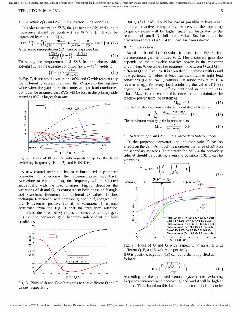
In Fig. 7, describes the variations of Ф and G with respect to ψ
for different Q values. It is seen that Ф goes to the negative
value when the gain more than unity at light load conditions.
So, it can be assumed that ZVS will be lost in the primary side
switches if G is larger than one.
Fig. 7. Plots of Ф and G with regards to ψ for the fixed
switching frequency (F = 1.2), and K (K=0.6).
A new control technique has been introduced in proposed
converter to overcome the aforementioned drawback.
According to equation (14), the frequency will be selected
sequentially with the load changes. Fig. 8, describes the
variations of Ф and G, as compared to both phase shift angle
and switching frequency for different Q values. In this
technique fs increases with decreasing load i.e. fs changes until
the Ф becomes positive for all ψ variations. It is also
confirmed from the Fig. 8, that the frequency selection
minimized the effect of Q values on converter voltage gain
(G) i.e. the converter gain becomes independent on load
conditions.
Fig. 8. Plots of Ф and G with regards to ψ at different Q and F
values respectively.
But Q (full load) should be low as possible to have small
inductive reactive components. Moreover, the operating
frequency range will be higher under all loads due to the
selection of small Q (full load) value. So, based on the
discussion above, Q =2.5 at full load has been selected.
B. Gain Selection
Based on the full load Q value, it is seen from Fig. 8, that,
the maximum gain is limited to 2. The maximum gain also
depends on the allowable reactive power in the converter
circuit. Fig. 9, describes the relationship between ϴ and G for
different Q and F values. It is seen that ϴ increases with G and
in a particular G value, ϴ becomes maximum at light load
conditions (i.e at low Q values) .To allow maximum 10%
reverse energy for every load condition, the value of ϴ (in
degree) is limited to 58.680 as mentioned in equation (11).
Thus, Mmax is chosen for this converter to minimize the
reactive power from the system as,
Mmax =1.8 (15)
So, the transformer turn’s ratio is calculated as follows:
n = Np
Ns =
Mmax . Vin−min
2⁄
Vo = 15 : 4 (16)
The minimum voltage gain is obtained as,
Mmin = n . Vo
Vin−max2⁄ = 0.9 (17)
C. Selection of K and ZVS in the Secondary Side Switches
In the proposed converter, the inductor ratio K has no
effects on the gain. Although, K increases the range of ZVS on
the secondary switches. To maintain the ZVS in the secondary
side, ϴ should be positive. From the equation (10), it can be
written as,
[
ϴ = tan−1 (𝐵
𝐴− √
1
𝐴2𝐺2 − 1)
where, A = 𝑄(𝐹2 − 1)
𝐹;B = 1 + 𝐾 − 𝑘
𝐹2⁄
(18)
Fig. 9. Plots of ϴ and G with respect to Phase-shift ψ at
different Q, F, and K values respectively.
If ϴ is positive, equation (18) can be further simplified as
follows
K >⎹ [A.(√
1
A2𝐆2 −1)−1]
1− 1
F2
⎹ (19)
According to the proposed control system, the switching
frequency increases with decreasing load, and it will be high at
no load. Thus, based on this fact, the inductor ratio K has to be
0885-8993 (c) 2016 IEEE. Personal use is permitted, but republication/redistribution requires IEEE permission. See http://www.ieee.org/publications_standards/publications/rights/index.html for more information.
This article has been accepted for publication in a future issue of this journal, but has not been fully edited. Content may change prior to final publication. Citation information: DOI 10.1109/TPEL.2016.2643006, IEEETransactions on Power Electronics
TPEL-REG-2016-08-1512
6
calculated. The inductor ratio K at extreme condition like
Q=2.5 (i.e: full load) with, Mmin =0.9 and F = 1.105(from
equation (14)), calculated as,
K > 0.0429 (20)
It can be confirmed from Fig. 9, the gain of the converter is
unaffected by the inductor ratio K. It is observed that a small
Lm (i.e large K) is useful to extend the ZVS range on the
secondary side. But with large k value, the reverse energy will
be more due to the high value of ϴ especially at light load
condition. This reverse energy will increase the conduction
losses which are responsible for reducing the system
efficiency. Thus, the choice of high K value is not reasonable,
otherwise efficiency will be degraded. So, K=0.043 has to be
selected in this system to reduce excessive reverse energy as
well as to get suitable gain with ZVS.
Fig. 10. Plots of Ф, ϴ and G with regards to ψ.
With k = 0.043, the relationship among Ф, ϴ, and G with
regards to ψ for different Q and F values have been plotted in
Fig.10. It can be confirmed that Ф and ϴ are always positive
for the whole operating voltage gain range i.e ZVS transition
on the both primary and secondary side switches is maintained
when G is between 0.9 to 1.8. It is also confirmed that the
value of ϴ at the maximum gain point is equal to 57.290 (1 in
radian) which indicates that the ratio between the reactive
power to output power remains within 10% for all phase shift
angles according to the desired gain range.
Finally with the help of equations (1-3, 5) resonant tank
elements are calculated as follows:
Lr = 8QRLn2
π2ωr (21)
Cr = π2
8QRLωrn2 (22)
Lm = Lr
K (23)
The design specifications of the proposed converter are
summarized in Table I. TABLE I
SPECIFICATIONS OF THE DESIGNED CONVERTER
Parameter - Symbol Value - unit
Input voltage, Vin 200 - 400 V
Output voltage, Vo 48 V
Resonant Inductor, Lr 241.58 µH
Resonant Capacitor, Cr 55.93 nF
Parallel Inductor, Lm 5.61 mH
Rated load Resistance (full load) 2.304 Ω
Rated output power, Po 1kw
V. CONTROL SCHEME
Switching frequency has to be selected in every load condition
to ensure the ZVS in the primary side switches. This
frequency selection minimized the effect of loaded Q values
and kept the converter voltage gain characteristics identical for
every phase shifted angle. Later, the phase shift angle (ψ) can
be regulated the output voltage to the desired one with regards
to input voltages. The method used to obtain such a signal is
shown in Fig. 11.
Fig. 11. Simplified block diagram of the proposed FAPSM
control.
The control law has been implemented on DSP
TMS320F28335 from TI. The DSP samples the inputs by its
A/D input and controls the switching frequency (fs) and phase
shift by simply changing the register values. Thus, the output
can be regulated to the desired value based on the flow chart
shown in Fig. 12.
Begin
Output voltage is equal to the
desire value
Input impedance angle > 0 ,
(for all phase shift angle)
Voltage gain is above 1.8
Increase the switching frequency
Decrease the switching
frequency
Output voltage controller
Keep the switching
frequency and phase
shift constant
Input
Voltage , Vin
(Output current) Io
Set the switching frequency
and phase shift
Yes
No
Yes
No
Yes
No
Phase shift
Fig. 12. Output voltage regulation using the proposed control
scheme.
VI. COMPARISON OF CONVERTER TOPOLOGIES
A comparison of five topologies is illustrated in Table II.
0885-8993 (c) 2016 IEEE. Personal use is permitted, but republication/redistribution requires IEEE permission. See http://www.ieee.org/publications_standards/publications/rights/index.html for more information.
This article has been accepted for publication in a future issue of this journal, but has not been fully edited. Content may change prior to final publication. Citation information: DOI 10.1109/TPEL.2016.2643006, IEEETransactions on Power Electronics
TPEL-REG-2016-08-1512
7
TABLE II
COMPARISON OF RESONANT CONVERTER TOPOLOGIES
Topologies DBSR LLC
converter
[16]
DAB LLC
converter
with new
control
scheme [17]
Three level
LLC resonant
converter
with PWAM
control [18]
DBSR LLC
converter with
phase shift
Control [29]
Proposed
LLC
resonant
converter
with FAPSM
Number of switches 8 8 12 4 6
Voltage stress across the
switches is equal to half of
the input voltage (for all load
and voltage gain)
No
(Equal to the
input voltage)
No
(Equal to the
input voltage)
No
(Depends on
the voltage
gain )
No
(Equal to the
input voltage)
Half of the
input voltage
Number of transformer’s
secondary windings
1 1 1 2 2
ZVS Primary
bridge: ZVS
Secondary
bridge: ZCS
Primary
bridge: ZVS
Secondary
bridge: ZCS
Primary side:
ZVS
Secondary
bridge: ZCS
Primary side:
ZVS
Secondary
bridge: ZVS
Primary side:
ZVS
Secondary
bridge: ZVS
Reactive power control No Yes No No Yes
Flying capacitor No No Yes No No
Modulation PSM FFPWM PWAM PSM FAPSM
Gain range Unity gain Narrow Wide Unity gain only Wide
Input range 110 V 75-130 V 240-480 V 200 V 200-400 V
Output Power 100V/ 2 A 400 V/2.5A 60 V/ 20 A 48 V/6.25 A 48V/20.83A
VII. SIMULATION AND EXPERIMENT RESULTS
To verify the analytical result, the proposed converter has
been simulated in MATLAB. The simulation is carried out
under maximum and minimum input voltage with the full load
and 20% load conditions. Fig. 13, (a-d) shows the Vr , Ir, Vt ,
It, Vcr and I2 over different inputs and load conditions.
Operating frequency changes as the load only and remains
constant for the fixed load regardless of input voltages. To
remain the output voltage constant, ψ changes with input
variations irrespective of load conditions. It is seen that ϴ
becomes higher at low input voltage, which increases the
reverse power as well as decreases the efficiency. Therefore,
for the same output power, I2 shows the more negative
percentage at 200 V than 400 V input. It is also observed that
all the stresses across the resonant tank become higher at low
input voltage condition. ZVS can be verified by evaluating the
phase angles of Ir and It with respect to Vr and Vt respectively.
Time (second)
Fig. 13(a). Simulation waveforms of proposed converter
under 400V input, 48V output and full load condition.
Time (second)
Fig. 13(b). Simulation waveforms of proposed converter
under 200V input, 48V output and full load condition.
0.09995 0.09998 0.09999 0.1
-400
0
400
Vr(V)
0.09996466 0.09998 0.09999 0.1
-15
0
15
Ir(A)
0.09995 0.09998 0.09999 0.1
-180
0
180
Vt(V)
0.09996587 0.09998 0.09999 0.1
-15
0
15
It(A)
0.09995 0.09996 0.09997 0.09998 0.09999 0.1
-400
0
800
Vcr
(V)
0.09995 0.09996 0.09997 0.09998 0.09999 0.1
-50
35
I2(A)
0.09995 0.0999646 0.09998 0.09999 0.1
-200
0
200
Vr(V)
0.09998 0.09999 0.1
-20
0
20
Ir(A)
0.0999651 0.09998 0.09999 0.1
-180
0
180
Vt(V)
0.09995 0.09998 0.09999 0.1
-20
0
20
It(A)
0.09995 0.09996 0.09997 0.09998 0.09999 0.1
-750
0
1200
Vcr
(V)
0.09995 0.09996 0.09997 0.09998 0.09999 0.1-80
0
80
I2(A)
0.09997 0.0999821 0.09999 0.1
-400
0
400
Vr(V)
0.09997 0.09999 0.1
-2
0
2
Ir(A)
0.09997 0.09999 0.1
-180
0
180
Vt(V)
0.09997 0.09998288 0.09999 0.1
-202
It(A)
0885-8993 (c) 2016 IEEE. Personal use is permitted, but republication/redistribution requires IEEE permission. See http://www.ieee.org/publications_standards/publications/rights/index.html for more information.
This article has been accepted for publication in a future issue of this journal, but has not been fully edited. Content may change prior to final publication. Citation information: DOI 10.1109/TPEL.2016.2643006, IEEETransactions on Power Electronics
TPEL-REG-2016-08-1512 8
Time (second)
Fig. 13(c). Simulation waveforms of proposed converter
under 400V input, 48V output and 20% load condition.
Time (second)
Fig. 13(d). Simulation waveforms of proposed converter
under 200V input, 48V output and 20% load condition.
A prototype converter has been built and tested in the lab to
verify the proposed method. The resonant frequency can be
chosen high to reduce the parasitic effects in the circuit. N95
material based ferrite core (PQ 50/50) has been used to build
the HF transformer. With the proper design, the resulted
magnetizing inductance has been set to 5.61 mH. This high
value of magnetizing inductance reduces the conduction loss
of the transformer. HEXFET MOSFET IRFR-4620PbF and
MOSFET IPP200N15N3G are adopted as the primary and
secondary switches respectively. The experimental waveforms
of a proposed converter are shown in Fig. 14 (a-f). Most of the
results have similarities with simulation and theoretical
calculations. As shown in Fig. 14 (e), soft switching can be
achieved in primary and secondary side switches. Since
ZVZCS is observed on both sides during turn-on, thus the
high-frequency turn-on switching losses become negligible.
There are no considerable voltage spikes across the switch
voltage (Vds) which signifies the ZVS turn-off transition. The
switch current commutates to the lossless snubbing capacitor
instead of the switch itself and the MOSFET becomes
switched off fully before the drain to source voltage rises
significantly above zero. Due to ZVS, turn-off transition
switching losses are reduced to the very small value. It is also
seen that the voltage stress of the primary switches is about
200 V, which is half of the input voltage. As a result, the low
voltage rated MOSFET with low Rdson is employed to reduce
the conduction losses.
5µs/div
Ir
Vr
Vt
It
2µs/div
5µs/div
Vcr
I2
Vt
It
Ir
Vr
Fig. 14(a). Experimental waveforms under 400V input , 48V
output and full load condition (Vr (200 V/div), Ir (10A/div), Vt
Fig. 14(d). Experimental waveforms under 200V input , 48V
output and 20% load condition (Vr (100 V/div), Ir (4A/div), Vt
(200V/div), It (4A/div), Vcr (100V/div), I2 (12A/div)).
ZVZCS-turn onZVS-turn off 5µs/div
Vds
Id
ZVS-turn off ZVZCS-turn on5µs/div
Vds
Id
(a) (b)
Fig. 14(e). Switching waveforms of (400Vand full load
condition), (a) Primary side switch (Vds (100 V/div), Id
(10A/div), (b) Secondary side switch (Vds (50V/div), Id
(20A/div).
0.09997 0.09998 0.09999 0.1100
300
Vcr
(V)
0.09997 0.09998 0.09999 0.1
-3
0
7
I2(A)
0.09997 0.0999768 0.09999 0.1
-200
0
200
Vr(V)
0.09997 0.09999 0.1
-5
0
5
Ir(A)
0.09997 0.0999794 0.09999 0.1
-180
0
180
Vt(V)
0.09997 0.09999 0.1
-5
0
5
It(A)
0.09997 0.09998 0.09999 0.1-100
0
300
Vcr
(V)
0.09997 0.09998 0.09999 0.1-20
0
20
I2(A)
0885-8993 (c) 2016 IEEE. Personal use is permitted, but republication/redistribution requires IEEE permission. See http://www.ieee.org/publications_standards/publications/rights/index.html for more information.
This article has been accepted for publication in a future issue of this journal, but has not been fully edited. Content may change prior to final publication. Citation information: DOI 10.1109/TPEL.2016.2643006, IEEETransactions on Power Electronics
TPEL-REG-2016-08-1512 9
5µs/div 5µs/divIt*
Ir*
Vr
Vt
Vcr
I2*
Fig. 14(f). Experimental waveforms of reverse power flow at
48 V input, 400 V output, full load condition (Ir*= -Ir, It
*= -It ,
I2* = - I2 ) (Vr (200V/div), Ir
* (10A/div), Vt (200V/div), It
*
(10A/div), Vcr (400V/div), I2* (20A/div)).
For the reverse power flow, the control variable ψ should be
negative. Fig. 14(f) shows the waveforms of Vr , Ir* (Ir = -
Ir*), Vt , It* (It = -It*) ,Vcr and I2* (I2 = -I2*) for the ψ = -29.50.
ZVS operation can be confirmed by checking the phase angle
of Ir* and It* with respect to Vr and Vt.
Fig. 15 represents the estimated power loss breakdown for
different inputs and load conditions. It can be seen that
conduction losses are the largest proportion of the total power
loss. It is also seen that conduction losses are increased at the
low input voltage condition. The efficiency of the converter
under 400V and 200V on different load conditions is shown in
Fig.16. As it can be seen, the efficiency becomes higher all
over the load range at 400V due to the low value of circulating
current in the secondary side. But, efficiency degraded at
200V as compared to 400V because of higher circulating
current (or reactive power) still exists on the secondary side.
Calculated efficiency is slightly more than the measured value.
However, the variation of efficiency from no load to full load
for maximum input voltage is narrow.
(a)
(b)
Fig. 15. Loss breakdown for (a) 400V input (b) 200V input
Fig. 16. Measured efficiency of the proposed LLC resonant
converter.
To validate the steady-state analysis a comparison of all
important angles obtained from theoretical calculations,
simulations and experiments are given in Table III. All the
results are almost close to each other and also all angles follow
the increasing and decreasing trend according to phase shift
angle. TABLE III
COMPARISON OF DIFFERENT ANGLES
𝜓 o Ф
o ϴ
o
400V, full
load
condition
Theoretical 27.5 22.99 5.39
Simulation 27.5 21.12 5.71
Experimental 29.5 24.2 6.1
400V, 20%
load
condition
Theoretical 27.5 23.13 7.38
Simulation 27.5 20.79 7.1
Experimental 29.5 23.68 7.5
200V, full
load
condition
Theoretical 65 8.12 57.16
Simulation 65 8.61 55.12
Experimental 68 12.2 58.3
200V, 20%
load
condition
Theoretical 65 8.03 57.74
Simulation 65 11.31 54.53
Experimental 68 12.1 58.4
VIII. CONCLUSION
In this paper, a variable frequency phase shift modulation
control for a DAB LLC resonant converter has been
incorporated. This control strategy makes the converter
operating at a wide gain range with ZVS over all load
conditions. The combination of two half bridge connected in
series on the inverter side reduces the voltage stress across
each switch, which also makes the converter capable of
operating at high-voltage applications. The voltage stresses
remain half of the input voltage over all load variations. With
the proposed control, the voltage gain becomes independent of
Q and K values. Thus, the process of parameter design can be
simplified. The magnetizing inductance has been calculated as
high to reduce the conduction loss. It also reduced the
circulating current (or, reactive power) from the secondary
side even at light load condition, which increased the
efficiency as compared to conventional DAB LLC resonant
converter. The performance of the proposed LLC resonant
converter is experimentally verified with 200-400V input and
48V output converter prototype. Therefore, the proposed
converter becomes a good candidate for variable input and
constant output voltage applications.
80
85
90
95
100
10 20 50 80 100
Eff
icie
ncy
(%
)
Load (%)
400 V input
200 V input
0885-8993 (c) 2016 IEEE. Personal use is permitted, but republication/redistribution requires IEEE permission. See http://www.ieee.org/publications_standards/publications/rights/index.html for more information.
This article has been accepted for publication in a future issue of this journal, but has not been fully edited. Content may change prior to final publication. Citation information: DOI 10.1109/TPEL.2016.2643006, IEEETransactions on Power Electronics
TPEL-REG-2016-08-1512 10
REFERENCES
[1] D. Costinett, D. Maksimovic, and R. Zane, "Design and Control for
High Efficiency in High Step-Down Dual Active Bridge Converters Operating at High Switching Frequency," IEEE Transactions on Power
Electronics, vol. 28, pp. 3931-3940, 2013.
[2] S. P. Engel, N. Soltau, H. Stagge, and R. W. D. Doncker, "Dynamic and Balanced Control of Three-Phase High-Power Dual-Active Bridge DC-
DC Converters in DC-Grid Applications," IEEE Transactions on Power
Electronics, vol. 28, pp. 1880-1889, 2013. [3] F. Krismer and J. W. Kolar, "Efficiency-Optimized High-Current Dual
Active Bridge Converter for Automotive Applications," IEEE
Transactions on Industrial Electronics, vol. 59, pp. 2745-2760, 2012. [4] F. Z. Peng, L. Hui, S. Gui-Jia, and J. S. Lawler, "A new ZVS
bidirectional DC-DC converter for fuel cell and battery application,"
IEEE Transactions on Power Electronics, vol. 19, pp. 54-65, 2004. [5] S. Inoue and H. Akagi, "A Bidirectional DC-DC Converter for an
Energy Storage System With Galvanic Isolation," IEEE Transactions on
Power Electronics, vol. 22, pp. 2299-2306, 2007.
[6] H. Qin and J. W. Kimball, "Generalized Average Modeling of Dual
Active Bridge DC-DC Converter," IEEE Transactions on Power
Electronics, vol. 27, pp. 2078-2084, 2012. [7] B. Zhao, Q. Song, W. Liu, G. Liu, and Y. Zhao, "Universal High-
Frequency-Link Characterization and Practical Fundamental-Optimal
Strategy for Dual-Active-Bridge DC-DC Converter Under PWM Plus Phase-Shift Control," IEEE Transactions on Power Electronics, vol. 30,
pp. 6488-6494, 2015. [8] A. K. Jain and R. Ayyanar, "PWM control of dual active bridge:
comprehensive analysis and experimental verification," in Industrial
Electronics, 2008. IECON 2008. 34th Annual Conference of IEEE, 2008, pp. 909-915.
[9] H. Zhou and A. M. Khambadkone, "Hybrid Modulation for Dual-
Active-Bridge Bidirectional Converter With Extended Power Range for Ultracapacitor Application," IEEE Transactions on Industry
Applications, vol. 45, pp. 1434-1442, 2009.
[10] B. Zhao, Q. Song, and W. Liu, "Efficiency Characterization and
Optimization of Isolated Bidirectional DC-DC Converter Based on
Dual-Phase-Shift Control for DC Distribution Application," IEEE
Transactions on Power Electronics, vol. 28, pp. 1711-1727, 2013. [11] B. Zhao, Q. Song, and W. Liu, "Power Characterization of Isolated
Bidirectional Dual-Active-Bridge DC-DC Converter With Dual-Phase-
Shift Control," IEEE Transactions on Power Electronics, vol. 27, pp. 4172-4176, 2012.
[12] G. Oggier, G. O. Garc, x00Ed, and A. R. Oliva, "Modulation strategy to
operate the dual active bridge DC-DC converter under soft switching in the whole operating range," IEEE Transactions on Power Electronics,
vol. 26, pp. 1228-1236, 2011.
[13] H. Bai and C. Mi, "Eliminate Reactive Power and Increase System Efficiency of Isolated Bidirectional Dual-Active-Bridge DC-DC
Converters Using Novel Dual-Phase-Shift Control," IEEE Transactions
on Power Electronics, vol. 23, pp. 2905-2914, 2008. [14] Y. Gang, P. Dubus, and D. Sadarnac, "Double-Phase High-Efficiency,
Wide Load Range High- Voltage/Low-Voltage LLC DC/DC Converter
for Electric/Hybrid Vehicles," IEEE Transactions on Power Electronics, vol. 30, pp. 1876-1886, 2015.
[15] W. Hongfei, M. Tiantian, G. Xun, and X. Yan, "A Secondary-Side
Phase-Shift-Controlled LLC Resonant Converter With Reduced Conduction Loss at Normal Operation for Hold-Up Time Compensation
Application," IEEE Transactions on Power Electronics, vol. 30, pp.
5352-5357, 2015. [16] X. Li and A. K. S. Bhat, "Analysis and Design of High-Frequency
Isolated Dual-Bridge Series Resonant DC/DC Converter," IEEE
Transactions on Power Electronics, vol. 25, pp. 850-862, 2010. [17] J. Tianyang, Z. Junming, W. Xinke, S. Kuang, and W. Yousheng, "A
Bidirectional LLC Resonant Converter With Automatic Forward and
Backward Mode Transition," IEEE Transactions on Power Electronics, vol. 30, pp. 757-770, 2015.
[18] J. Tianyang, Z. Junming, W. Xinke, S. Kuang, and W. Yousheng, "A
Bidirectional Three-Level LLC Resonant Converter With PWAM Control," IEEE Transactions on Power Electronics, vol. 31, pp. 2213-
2225, 2016.
[19] R. Severns, "Topologies for three element resonant converters," in Applied Power Electronics Conference and Exposition, 1990. APEC '90,
Conference Proceedings 1990., Fifth Annual, 1990, pp. 712-722.
[20] X. Fang, H. Hu, Z. J. Shen, and I. Batarseh, "Operation Mode Analysis
and Peak Gain Approximation of the LLC Resonant Converter," IEEE Transactions on Power Electronics, vol. 27, pp. 1985-1995, 2012.
[21] R. Beiranvand, B. Rashidian, M. R. Zolghadri, and S. M. H. Alavi, "A
Design Procedure for Optimizing the LLC Resonant Converter as a Wide Output Range Voltage Source," IEEE Transactions on Power
Electronics, vol. 27, pp. 3749-3763, 2012.
[22] X. Sun, X. Li, Y. Shen, B. Wang, and X. Guo, "A Dual-Bridge LLC Resonant Converter with Fixed-Frequency PWM Control for Wide Input
Applications," IEEE Transactions on Power Electronics, vol. PP, pp. 1-
1, 2016. [23] L. Il-Oun and M. Gun-Woo, "Analysis and Design of a Three-Level
LLC Series Resonant Converter for High-and Wide-Input-Voltage
Applications," IEEE Transactions on Power Electronics, vol. 27, pp. 2966-2979, 2012.
[24] G. Yilei, L. Zhengyu, H. Lijun, Q. Zhaoming, and H. Guisong, "Three-
level LLC series resonant DC/DC converter," IEEE Transactions on Power Electronics, vol. 20, pp. 781-789, 2005.
[25] L. Wuhua, L. Qingjing, M. Ye, Z. Sheng, H. Xiangning, and X.
Changliang, "Flying-Capacitor-Based Hybrid LLC Converters With
Input Voltage Autobalance Ability for High Voltage Applications,"
IEEE Transactions on Power Electronics, vol. 31, pp. 1908-1920, 2016
[26] Y. Bo, F. C. Lee, A. J. Zhang, and H. Guisong, "LLC resonant converter for front end DC/DC conversion," in Applied Power Electronics
Conference and Exposition, 2002. APEC 2002. Seventeenth Annual
IEEE, 2002, pp. 1108-1112 vol.2. [27] G. Ivensky, S. Bronshtein, and A. Abramovitz, "Approximate Analysis
of Resonant LLC DC-DC Converter," IEEE Transactions on Power Electronics, vol. 26, pp. 3274-3284, 2011.
[28] T. Jiang, X. Chen, J. Zhang, and Y. Wang, "Bidirectional LLC resonant
converter for energy storage applications," in Applied Power Electronics Conference and Exposition (APEC), 2013 Twenty-Eighth Annual IEEE,
2013, pp. 1145-1151.
[29] L. Xiaodong, "A LLC-Type Dual-Bridge Resonant Converter: Analysis, Design, Simulation, and Experimental Results," IEEE Transactions on
Power Electronics , vol. 29, pp. 4313-4321, 2014.
S M SHOWYBUL ISLAM SHAKIB received the B.Sc. degree in electrical
and electronic engineering from the
Rajshahi University of Engineering and
Technology, Rajshahi, Bangladesh in
2012. He is currently pursuing the
M.Eng.Sc. degree in the Power
Electronics and Renewable Energy
Research Laboratory, Department of
Electrical Engineering , University of Malaya, Kuala Lumpur,
Malaysia.
His research interests include LLC resonant DC/DC
converter, Power conversion and control of power converters.
Saad Mekhilef (M’01–SM’12) received
the B.Eng. in electrical engineering from
the University of Setif, Setif, Algeria, in
1995, and the Master’s degree in
engineering science and the Ph.D. degree
in electrical engineering from the
University of Malaya, Kuala Lumpur,
Malaysia, in 1998 and 2003, respectively.
He is currently a Professor and the
Director of the Power Electronics and Renewable Energy
Research Laboratory, Department of Electrical Engineering,
University of Malaya. He is the author or coauthor of more
than 300 publications in international journals and conference
proceedings. His research interests include power, control of
power converters, renewable energy, and energy efficiency.