Page 1
A HIGH CMRR INSTRUMENTATION AMPLIFIER FOR
BIOPOTENTIAL SIGNAL ACQUISITION
A Thesis
by
Reza Muhammad Abdullah
Submitted to the Office of Graduate Studies of
Texas A&M University
in partial fulfillment of the requirements for the degree of
MASTER OF SCIENCE
May 2011
Major Subject: Electrical Engineering
Page 2
A HIGH CMRR INSTRUMENTATION AMPLIFIER FOR
BIOPOTENTIAL SIGNAL ACQUISITION
A Thesis
by
Reza Muhammad Abdullah
Submitted to the Office of Graduate Studies of
Texas A&M University
in partial fulfillment of the requirements for the degree of
MASTER OF SCIENCE
Approved by:
Chair of Committee, Edgar Sanchez-Sinencio
Committee Members, Hamid A. Toliyat
Samuel Palermo
Duncan Henry M. Walker
Head of Department, Costas N. Georghiades
May 2011
Major Subject: Electrical Engineering
Page 3
iii
ABSTRACT
A High CMRR Instrumentation Amplifier for Biopotential
Signal Acquisition. (May 2011)
Reza Muhammad Abdullah, B.Sc., Kwame Nkrumah University of Science & Tech
Chair of Advisory Committee: Dr. Edgar Sanchez-Sinencio
Biopotential signals are important to physicians for diagnosing medical conditions in
patients. Traditionally, biopotentials are acquired using contact electrodes together with
instrumentation amplifiers (INAs). The biopotentials are generally weak and in the
presence of stronger common mode signals. The INA thus needs to have very good
Common Mode Rejection Ratio (CMRR) to amplify the weak biopotential while
rejecting the stronger common mode interferers. Opamp based INAs with a resistor-
capacitor feedback are suitable for acquiring biopotentials with low power and low noise
performance. However, CMRR of such INA topologies is typically very poor.
In the presented research, a technique is proposed for improving the CMRR of opamp
based INAs in RC feedback configurations by dynamically matching input and feedback
capacitor pairs. Two instrumentation amplifiers (one fully differential and the other fully
balanced fully symmetric) are designed with the proposed dynamic element matching
scheme.
Post layout simulation results show that with 1% mismatch between the limiting
capacitor pairs, CMRR is improved to above 150dB when the proposed dynamic
element matching scheme is used. The INAs draw about 10uA of quiescent current from
a 1.5 dual power supply source. The input referred noise of the INAs is less than
3uV/ 𝐻𝑧.
Page 4
iv
ACKNOWLEDGEMENTS
First, I would like to thank my committee chair, Dr. Edgar Sanchez-Sinencio for his
expert guidance and for encouragement he gave me during the time I have spent
pursuing a Master’s degree at Texas A&M University. My thanks also goes to my
committee members and all the professors in the Analog & Mixed Signal Center of
Texas A&M University for all the technical support I have received during my stay as
part of the group. I also extend my gratitude to Texas Instruments Incorporated for
initiating the AAURP (African Analog University Relations Program) initiative through
which I was introduced to Analog Integrated Circuits. My thanks also go to Texas
Instruments for sponsoring my Master’s education here at Texas A&M University. To
my fellow colleagues and office mates of the Analog and Mixed Signal Center (AMSC),
thank you for all the help and understanding shown to me at all times. Finally, I want to
acknowledge my parents, siblings and all family members who have in numerous ways
supported and encouraged me throughout my pursuit of Electrical Engineering as a
profession. Thank you all.
Page 5
v
TABLE OF CONTENTS
Page
ABSTRACT ...................................................................................................................... iii
ACKNOWLEDGEMENTS .............................................................................................. iv
TABLE OF CONTENTS ................................................................................................... v
LIST OF FIGURES .......................................................................................................... vii
LIST OF TABLES ............................................................................................................ ix
1. INTRODUCTION ........................................................................................................ 1
A. Amplifiers, Operational Amplifiers and Instrumentation Amplifiers .............. 2
B. Applications of Instrumentation Amplifiers ..................................................... 4
C. Classes of Instrumentation Amplifiers ........................................................... 12
2. CMRR OF INSTRUMENTATION AMPLIFIERS ................................................... 16
A. Definition of CMRR ....................................................................................... 17
B. CMRR Case Study .......................................................................................... 18
C. Capacitive vs. Resistive Mismatch of RC Feedback Amplifiers .................... 23
D. Previously Published Works on Biopotential Amplifiers .............................. 28
3. PROPOSED INSTRUMENTATION AMPLIFIERS ................................................ 33
A. Dynamic Element Matching ........................................................................... 33
B. Concept of Proposed INAs ............................................................................. 34
C. Dynamically Matched RC Feedback Fully Differential INA ......................... 40
D. Dynamically Matched RC Feedback FBFS INA ........................................... 41
E. System Level Design ...................................................................................... 43
F. Transistor Level Design .................................................................................. 50
4. LAYOUT STRATEGY AND SIMULATION RESULTS ........................................ 63
A. Layout ............................................................................................................. 63
B. Results – Dynamically Matched Fully Differential INA ................................ 67
C. Results – Dynamically Matched FBFS INA .................................................. 73
5. SUMMARY AND CONCLUSION ........................................................................... 79
Page 6
vi
Page
REFERENCES ................................................................................................................. 80
VITA ................................................................................................................................ 82
Page 7
vii
LIST OF FIGURES
FIGURE Page
1-1 Block Diagram of an Amplifier and Operational Amplifier ............................ 2
1-2 Applications of Instrumentation Amplifiers .................................................... 4
1-3 Amplitude and Frequency Characteristics of Some Bipotentials .................... 6
1-4 Electrical Model of Skin-Electrode Interface .................................................. 7
1-5 Electrostatic Interference to Human Body ..................................................... 10
1-6 Three Opamp Instrumentation Amplifier ...................................................... 12
1-7 Concept of Current Balancing INA………………………..……………………14
1-8 More Accurate Representation of Current Balancing INA ............................ 15
2-1 Block Diagram of Single Ended and Fully Differential Amplifiers .............. 16
2-2 Opamp with General Impedance Feedback Configuration ............................ 18
2-3 Common Mode Gain vs. Percentage Mismatch in Y1……………….…..…...21
2-4 Common Mode Gain vs. Percentage Mismatch in Y4……………….…..…...21
2-5 RC Feedback Amplifier Used for EKG Signal Acquisition .......................... 22
2-6 Common Mode Gain vs. Frequency of an RC Feedback Amplifier .............. 25
2-7 Common Mode Gain vs. Frequency for Varying Capacitor Mismatch ......... 26
2-8 Biopotential Amplifier with MOS-Bipolar Pseudo Resistor Element.....…...28
2-9 Two Stage INA with Fully Differential Outputs ........................................... 30
2-10 Concept of ACCIA ....................................................................................... 31
2-11 Implementation of ACCIA………….…..………….……………………….…..32
3-1 Simple Voltage Divider Using Resistors ....................................................... 33
3-2 Fully Differential Version of INA ................................................................ 35
3-3 Fully Balanced Fully Symmetric Version of INA ......................................... 35
3-4 Swapping of Capacitors to Reverse Polarity of Mismatch ............................ 37
3-5 Emulating the Effect of Swapping Capacitors Using ON/ OFF Switches ..... 38
3-6 Fully Differential Version of Dynamically Matched INA ............................. 40
Page 8
viii
FIGURE Page
3-7 Dynamically Matched FBFS INA ................................................................. 41
3-8 Test for FBFS Amplifier ................................................................................ 42
3-9 Inverting Opamp Configuration……………….…..…………………………....46
3-10 INA for Noise Analysis………………………………..…………….…..….......48
3-11 Transistor Level Schematic Diagram of Fully Differential Opamp ............. 50
3-12 Differential Frequency Response of Designed Opamp ................................ 53
3-13 Effect of Transistor M3 Sizing on Input Referred Noise .............................. 55
3-14 Common Mode Feedback Circuit for Opamp .............................................. 57
3-15 Transistor Level Schematic Diagram of Single Ended Opamp .................... 58
3-16 Two-phase Non-overlapping Clock Generator ............................................. 59
3-17 Outputs of Non-overlapping Clock Generator .............................................. 60
3-18 Snapshot of Non-overlapping Region of Clocks .......................................... 60
3-19 Incremental Resistance of Pseudo-resistor Element ..................................... 61
4-1 Top Level Layout of Fully Differential INA ................................................ 63
4-2 Top Level Layout of Dynamically Matched Fully Balanced FBFS INA ..... 64
4-3 Top Level Floor Plan of Proposed INAs in Die............................................ 65
4-4 Complete Layout of INAs in Silicon Die ..................................................... 66
4-5 Transient Simulation of Fully Differential INA ........................................... 67
4-6 Differential Mode Frequency Response of Dynamically Matched Fully
Differential INA ............................................................................................ 68
4-7 Common Mode Frequency Response ........................................................... 69
4-8 CMRR of Dynamically Matched Fully Differential INA ............................. 70
4-9 Output and Input Referred Noise of Dynamically Matched
Fully Differential INA ................................................................................... 71
4-10 Transient Simulation of Dynamically Matched FBFS INA.......................... 73
4-11 Magnitude and Phase of Dynamically Matched FBFS INA ......................... 74
4-12 Common Mode Gain of Dynamically Matched FBFS INA ......................... 75
4-13 CMRR of Dynamically Matched FBFS INA ................................................ 76
4-14 Output and Input Referred Noise of Dynamically Matched FBFS INA....... 77
Page 9
ix
LIST OF TABLES
TABLE Page
1-1 Properties of INAs vs. Opamps ............................................................................ 3
1-2 Electrical Characteristics of Commonly Used Electrodes .................................... 8
1-3 Typical Skin Impedance Parameters ..................................................................... 8
1-4 General Requirements of an EKG Amplifier ...................................................... 11
2-1 Typical Requirements of an EKG Signal Amplifier ........................................... 23
2-2 Typical Resistor and Capacitor Values for an EKG Amplifier .......................... 24
2-3 Common Mode Gain of RC Feedback Biopotential Amplifier at 50Hz ............ 27
3-1 Amplitude and Frequency Characteristics of EKG ............................................ 43
3-2 Target Specifications of EKG Signal Amplifier ................................................. 44
3-3 Final Component Values for Proposed INAs ..................................................... 45
3-4 Final Opamp Target Specifications……………….…..…………………………....49
3-5 Transistor Sizes for Fully Differential Opamp ................................................... 56
3-6 Transistor Sizes for CMFB Circuit ..................................................................... 57
3-7 Transistor Sizes for Single Ended Opamps in FBFS INA .................................. 58
3-8 Aspect Ratios of Static CMOS Gates ................................................................. 59
3-9 Aspect Ratios of Pseudo Resistor Element ......................................................... 62
3-10 Sizing of Switches ............................................................................................... 62
4-1 Summary of Results - Dynamically Matched Fully Differential INA ................ 72
4-2 Summary of Results - Dynamically Matched FBFS INA .................................. 78
5-1 Comparison of Results with Other Published Works ......................................... 79
Page 10
1
1. INTRODUCTION
The importance of bio-potential signals to physicians for diagnosing medical conditions
and also general in-patient/ out patient monitoring cannot be overestimated.
Electrocardiogram (EKG) signals - that is the bio-potential signal that results from
internal electrochemical processes within the heart – can be used to monitor a patients’
health condition. Electroencephalogram (EEG) and EMG (Electromyogram)
respectively are electrical signals resulting from the human brain activity and from
contraction/ relaxation of body muscles.
Traditionally, these signals are acquired using electrodes and amplified using
instrumentation amplifiers. Acquisition of these signals is done differentially while any
common mode component of the bio-potential is rejected. This is very essential because
the required bio-potentials are typically weak signals with low voltage levels where as
the likely common mode signals that are coupled with the bio-potentials are much larger
in amplitude. For instance, in EKG acquisition, signal amplitudes are typically in micro-
volt range with maximum values about 0.5mV. A 60Hz interference signal from the
supply mains is typically coupled to the differential electrodes and thus appears as a
common signal which is much larger in voltage compared to the desired EKG signal.
This signal is referred to as a common mode signal and has to be rejected where as the
differential EKG signals is acquired.
The ability of an instrumentation amplifier to amplify required differential signals while
rejecting unwanted common mode signals is quantified by its Common Mode Rejection
Ratio (CMRR). Instrumentation amplifier properties vary depending on its topology and
application.
This thesis follows the style of the IEEE Journal of Solid-State Circuits.
Page 11
2
The most common instrumentation amplifier is the 3 - Opamp instrumentation amplifier.
This topology though is not suitable for portable bio-potential signal monitoring since it
demands high power consumption and has very poor CMRR. The poor CMRR of the 3-
Opamp IA is due to the use of passive components in its feedback network. The CMRR
depends on the mismatch of these passive components and degrades very quickly with
slight percentage mismatch in these components.
Various Instrumentation amplifiers have been proposed for purposes of bio-potential
signal acquisition targeting low power, low noise and high CMRR specifications. Single
Opamp topologies such as [1] have the advantage of lower power consumption however
the problem of poor CMRR is not addressed. Current feedback topologies as in [2] and
[3] have better CMRR however the inaccuracy of the gain of such topologies makes
design of these amplifiers a little complex.
Figure 1-1 Block Diagram of an Amplifier and Operational Amplifier
A. Amplifiers, Operational Amplifiers and Instrumentation Amplifiers
The operational amplifier (opamp) is one of the most common circuits used in analog
electronic circuit design. Its uses are very wide and opamps are found in sorts of
applications from power management systems to RF circuits and data converters. As an
Page 12
3
ideal black box, the opamps magnifies the voltage difference between its inputs by
several orders. In more specific terms, the ideal opamp has infinite gain, with infinite
input impedance and zero output impedance. These properties are desirable in all
applications where opamps are used.
An amplifier is somewhat of a loose term implying any system or block that produces an
output quantity that is a scaled version of its input. The input could be a single ended
signal or the difference of two signals. More commonly, the output of an amplifier is a
scaled current or voltage. Current and voltage amplifiers can be built using opamps in
negative feedback configurations or using entirely different circuit topologies. Figure 1-1
shows the block diagrams of amplifiers and operational amplifiers.
Table 1-1 Properties of INAs vs. Opamps
Properties
Opamp
INA
Gain Very Large Finite
Gain Accuracy High Very High
CMRR High Very High
`Noise Low Very Low`
Instrumentation Amplifiers (INAs) are special amplifiers designed where long term
accuracy and stability of the amplifier is desired. They are difference amplifiers in that
they have two inputs, the difference of which is amplified to produce the desired output.
Most instrumentation amplifiers will have at least one opamp and some negative
feedback network to produce the desired fixed gain. However, it should be noted that
there are a few open loop INA topologies as well. INAs typically have very good
Page 13
4
common mode rejection ratio (CMRR) and high input impedances. Table 1-1 shows the
general properties of opamps versus instrumentation amplifiers.
B. Applications of Instrumentation Amplifiers
The characteristics of instrumentation amplifiers mentioned in the previous section make
them very suitable for Measurement and Test applications. Besides that they are used in
a host of sensor applications such as temperature and pressure sensing. INAs are also
used in biomedical fields. A typical example of such use is in the front end of
biopotential acquisition systems. Figure 1-2 shows four major application areas of
instrumentation amplifiers.
Figure 1-2 Applications of Instrumentation Amplifiers
For this research effort, we focus on using instrumentation amplifiers for acquiring
biopotential signals. Such instrumentation amplifiers are also known as biopotential
signal amplifiers.
Page 14
5
1. Biopotential Signal Acquisition
Biopotentials are very important to physicians in modern medical practice. These are
electrical signals generated as a result of electro-chemical processes that occur within the
human body. The kind of body cells involved in these electro-chemical processes
determine what biopotential signal is generated and its possible use to physicians. The
most common biopotentials are electroencephalogram (EEG), electrocardiogram (EKG)
and electromyogram (EMG). Electroencephalogram (EEG) is generated as a result of
neuron activity within the brain, EMG due to electrical activity of skeletal muscles and
EKG as a result of electrical impulses that are generated due to the pumping activity of
the heart.
The above mentioned biopotentials are generated due to combination of action potentials
from several cells associated with the tissue/ organ [4]. Each action potential is a cycle
of potential changes across the cell membrane. During a cells inactive state, its exhibits a
potential referred to as a resting potential. In this state, the membrane of the cell is more
permeable to K+ than Na+. As such, K+ has higher concentration within the cell in their
inactive state. This diffusion gradient across the cell membrane causes K+ ions to slowly
move across the membrane to the exterior, making the interior more negative with
respect to the exterior of the cell membrane, and thus building an electric field in the
process. This continues until equilibrium point when the electric field balances the K+
diffusion gradient. The voltage build up at this point is about 70mV. Any electrical
stimulation of the cell at this point makes it more permeable to Na+ and these Na+ ions
diffuse into the cell reducing the electric field to about 40mV. The cell membrane
becomes even more permeable to K+ at this point resulting in sharp diffusion of K+ into
the cell again until the electric field drops to zero volts thus returning the cell to its
resting potential. It is this cycle of events that is referred to as the action potential of a
cell [4].
Page 15
6
The different biopotentials have unique electrical characteristics which need to be
considered carefully when acquiring the signal. Most basic are the frequency range and
amplitude levels of the signal.
Figure 1-3 Amplitude and Frequency Characteristics of Some Biopotentials [1]
The spectrum of an EKG signal is mostly concentrated within 0.5 Hz to 150 Hz
frequency range. The amplitudes of EKG (ECG) signals vary from a low of 0.5mV to a
high of approximately 10mV. Figure 1-3 shows the amplitude and frequency
characteristics of some other biopotential signals. Note that the biopotentials in the dark
shaded boxes are acquired using invasive procedures. This will be mentioned in the next
section. LFPs (Local Field Potentials) are biopotentials obtained from the dendrons of
neural cells within the brain. EEG (Electroencephalogram) and EMG (Electromyogram)
are the result of electrochemical activity within the brain and skeletal muscle tissue
respectively.
Page 16
7
1.1. Model for Biopotential Electrodes
Biopotentials can be acquired invasively or non-invasively using electrodes. The
electrode is an interface between the body and the input of the instrumentation amplifier
or readout circuitry. This interface (transducer) is necessary because current conduction
in the body is a result of ionic movement whereas in the readout front end it is a result of
electron motion. The electrode is thus a metal – electrolyte interface. In simple terms a
chemical reaction occurs when the metal comes in contact with a specific electrolyte and
this reaction results in the generation of free electrons (an oxidation reaction). This
unsettles the neutrality of the metal – electrolyte interface and creates an electron
gradient across it resulting in current flow.
Figure 1-4 Electrical Model for Skin - Electrode Interface [4]
Electrodes could be wet, dry or non-contact electrodes. Wet electrodes usually have a gel
like substance that creates contact between the body and the electrode. These types are
Page 17
8
the most common and Ag/ AgCl in particular are in wide use. Dry electrodes do away
with the gel like substance thus the contact resistance at the body – electrode interface is
quite high. However these are more comfortable to use. Finally, non – contact electrode
no physical contact with the body and behave capacitively. In Figure 1-4 is the structure
and a linear electrical model for the skin – electrode interface. Actually in this model,
two interfaces are shown. First is the skin – sweat interface which is modeled as a
resistor in series with a capacitor – resistor parallel combination that includes a dc offset
voltage. The second is the interface between the sweat and the biopotential electrode.
Typical values of the R’s and C’s are shown in Tables 1-2 and 1-3.
Table 1-2 Electrical Characteristics of Commonly Used Electrodes
Electrode
Offset
Resistance
Capacitance
Ag/AgCl
0.1 – 50mV
1 – 10k ohms
100 – 150nF
Stainless Steel
1 – 50mV
3 – 12k ohms
< = 100nF
Table 1-3 Typical Skin Impedance Parameters
Impedance
Prepared Skin
Unprepared Skin
Subcutaneous Resistance
< = 120 ohms
< = 120 ohms
Stratum Resistance
Up to 100k ohms
1 – 2 M ohms
Shunt Capacitance
Up to 10nF
Up to 40nF
Page 18
9
1.2. Biopotential Amplifiers
The biopotential amplifier [5],[6] is the main block that amplifiers the weak biopotential
signals to levels that can be analyzed and used by physicians. The biopotential amplifier
however has to meet certain criteria so as not to corrupt the signal during the acquisition
process. It has been mentioned earlier in the previous sections that the biopotentials have
an embedded dc offset due to the difference in the half cell potentials of the electrodes
used to acquire the signal. The dc offset, also referred to as the Differential Electrode
Offset (DEO), has to be filtered out before or during the acquisition process to avoid
saturating the biopotential amplifier. Also, the amplifier should be able to selectively
amplify only the biopotential signal of interest while attenuating signals of any other
frequency. In other words, the biopotential amplifier should have frequency
characteristics suitable for kind of biopotential that is being acquired.
Also, since the biopotentials themselves are very weak signals, the input referred noise
of the biopotential amplifier should be very small to make the biopotentials detectable by
the acquisition system. Low noise of the biopotential amplifier is very critical. One more
very pertinent issue to be considered when designing instrumentation amplifiers is
interference from unwanted sources.
Electromagnetic and electrostatic interference from the mains of buildings are sources of
unwanted signals for biopotential acquisition systems [4]. Whenever an alternating
current flows through a conductor, an electromagnetic field (EM field) is generated
around the conductor, and when this EM field cuts across the loop of conductors and
electromotive force (EMF) is generated. This is the principle of operation of a generator.
A similar effect occurs when the mains current of a building generates an EM field and
this field in turn cuts through the loop formed by the human body, the leads between the
electrodes and the input of the biopotential amplifier, and the biopotential amplifier
itself. Thus an unwanted AC signal is generated that is common to both inputs of the
biopotential amplifier.
Page 19
10
On the other hand, unwanted interference can be due to electrostatic effects and this is
explained using the Figure 1-5. Cbp is the capacitance between mains and the human
body while Cbg is the capacitance between the body and ground. CISO is the capacitance
between the circuit ground the earth. Re1 and Re2 are the resistances of the circuit leads.
A displacement current, ID, flows into the body through these capacitances and splits
about equally between the isolation capacitance and the body to ground capacitance. The
voltage created as a result of this current and the ground resistance appears as a common
mode signal at the inputs of the biopotential amplifier.
Figure 1-5 Electrostatic Interference to Human Body [4]
Since the unwanted signals due to EMI and ESI are common mode, the biopotential
amplifier needs to have very good Common Mode Rejection properties. Common Mode
Rejection Ratio (CMRR) is therefore another very critical parameter for biopotential
amplifier.
Page 20
11
Besides these main critical specifications for the biopotential amplifier, power
consumption has to also be minimized for the acquisition system and this begins with
designing a low power biopotential amplifier. Also, to make the system more versatile, it
helps to design a biopotential amplifier that is reconfigurable for varying the gain and
frequency characteristics of the overall acquisition system.
In Table 1-4 are the EKG general requirements of a biopotential amplifier. The targeted
application is EKG acquisition. The specifications in this table are obtained from
published papers [1-3] in EKG amplifiers.
Table 1-4 General Requirements of an EKG Amplifier
Parameter General Specification
CMRR 70 dB
Input Referred Noise 2-3μV rms
Input Impedance > 5Mohm
Bandwidth 0.1 – 150 Hz
Gain 40 dB
Page 21
12
C. Classes of Instrumentation Amplifiers
There are many ways to implement instrumentation amplifiers [1-3],[7-10] to achieve
long term stability and efficiency. In general terms, we can classify most topologies
under the following 2 types.
Opamp based INAs
Current Balancing INAs
Figure 1-6 Three Opamp Instrumentation Amplifier [11]
Page 22
13
1. Opamp Based Instrumentation Amplifiers
Opamp based INAs, as the name implies, utilize opamps and feedback networks for
amplification and frequency shaping if necessary. The most common INA topology of
this kind is the 3-opamp instrumentation amplifier. This is shown in Fig 1-6.
The 3 opamp INA has two stages. The overall gain of the INA is split between the two
stages. In Figure 1-6, the two gain stages amplify the differential input signal by G1 and
G2 respectively.
G1 = v1
vd
= 1 + 2RF
RG
………………………………(1.1)
G2 = vo
v1
= R2
R1
…………………………………… 1.2
Gtotal = G1G2 = R2
R1
1 +2Rf
RG
……………………..(1.3)
Typically, the 2nd
stage is a unity gain stage and is only used as a difference amplifier. In
the first stage, common mode signal is transferred unaltered to the inputs of the 2nd
stage
difference amplifier. Ideally, this scenario would mean the INA has very good rejection
of common mode signals. However, the CMRR of this topology ultimately depends on
the proper matching of the passive components, resistors in this case. Assuming 40dB
differential gain, the resistors have to be matched to within 0.1% of each other to achieve
100dB of CMRR (Common Mode Rejection Ratio). Let ΔR = Rf – RG and Ac = common
mode gain. Then
Ac ≈ ∆R
Rf + RG
…………………………………..…(1.4)
Laser trimming is required to obtain decent CMRR using this topology. Besides, the use
of 3 opamps in this topology makes it a high power consuming topology and unsuitable
for low power application such as portable biopotential signal acquisition systems.
Page 23
14
2. Current Balancing Instrumentation Amplifiers
INAs of this topology can best be explained by the simplified diagram in Figure 1-7. The
input stage is a transconductance stage while the output is a transimpedance. The input
voltage appears across the input resistance and generates a current through it. By some
means, (examples of which will be discussed in the following section), this current is
mirrored into the output stage and flows through the output resistor and in the process
generating the output voltage signal. Thus under ideal conditions, the gain of this INA is
defined by the ratio of output to input resistors and the CMRR is independent of the
matching between these resistors.
Figure 1-7 Concept of Current Balancing INA
The CBIA (Current Balancing Instrumentation Amplifier) concept seems very simple
however the issue is how to copy the current from the input to output stage.
AvI = Gain (ideal) = R2
R1
………………………………… 1.5
The ideal case assumes that the buffers have no output resistance and that the current
source is ideal. A more accurate representation of the concept is shown in Figure 1-8.
Page 24
15
In this case the output resistances of the buffers are accounted for as well as the finite
output resistance of the current source.
Figure 1-8 More Accurate Representation of Current Balancing INA
The gain is defined as shown in equation 1.6.
Ava= Gain actual = ∆.R2
R1
……………………… 1.6
where ∆ = RcsR1
R1+ 2Rbuf R2+ Rcs ……………………..….(1.7)
Design & simulation of some CBIA topologies shows that the gain accuracy is usually
not good because exact mirrors of the input stage current are difficult to replicate in the
transimpedance output stage. In equation 1.7, Δ is some fraction less than 1. Δ
approaches 1 under ideal conditions when Rbuf is zero and Rcs is infinite. The design
procedure of the CBIA is also more complex than that of the opamp based INA
topologies. Examples of CBIAs are reported in [2],[3].
Page 25
16
2. CMRR OF INSTRUMENTATION AMPLIFIERS
Common Mode Rejection Ratio (CMRR) is an important specification for all amplifiers
with differential inputs including both single ended and fully differential output versions.
For amplifiers with single ended outputs, CMRR is the ratio of the differential gain of
the amplifier to the common mode gain of the amplifier. The differential gain of the
amplifier is defined as the gain when differential inputs are applied whereas the common
mode gain of the amplifier is the gain of the amplifier when a common signal is applied
to the two inputs.
Figure 2-1 Block Diagram of Single Ended and Fully Differential Amplifiers
For fully differential amplifiers, there are two definitions of CMRR and both of them are
important depending on the application of the amplifier. Figure 2-1 is a generic block
diagram of a single ended and a fully differential amplifier. The CMRR for these
amplifiers are defined in the next section.
Page 26
17
A. Definition of CMRR
Let the common mode input and output voltages of the amplifiers be defined as below.
vc = vin1 + vin2
2…………….………………………(2.1a)
vd=vin1 - vin2
2………….…………………………...(2.1b)
vod = vo1 - vo2
2………….………….………….……(2.1c)
voc = vo1 + vo2
2 ………………………………………(2.1d)
Using the definitions in equations 2.1a to 2.1d, the common mode rejection ratio of a
single ended and fully differential amplifiers are defined as in equations 2.2 and 2.3.
Single Ended Amplifier
CMRR = Ad
Ac
where Ad = vo
vd
and Ac = vo
vc
………(2.2)
Fully Differential Amplifier
CMRR = Ad
Acc
where Ad = vod
vd
and Acc = voc
vc
…………(2.3)
Notice the definition for the common mode gain Acc of a fully differential amplifier. It is
defined as the ratio of the common mode output voltage of the amplifier, to the applied
common mode input signal. Acc needs to be high to minimize the transfer of common
mode input signal to the next stages of the biopotential acquisition system.
Page 27
18
For EKG acquisition systems, CMRR required is at least 60dBs but state of the art
biopotential INAs have typical CMRRs between 60dB and 80dB with a few topologies
(mostly current balancing INA topologies) achieving CMRRs in the 100dB range. The
last mentioned INAs are more complex to design however. This large CMRR
specification is necessary to reject unwanted interferer signals which appear as common
mode signals at the input of the biopotential INA.
B. CMRR Case Study
Consider the feedback amplifier shown in Figure 2-2. It can be used for biopotential
acquisition when modified slightly.
Figure 2-2 Opamp with General Impedance Feedback Configuration
Page 28
19
1. CMRR Analysis of General Feedback Amplifier
For this analysis, we assume an ideal opamp therefore
A0→∞ and vn = vp
Performing nodal analysis on the circuit gives
vp Y2 + Y4 - Y2Vicm = 0
vn Y1 + Y3 -Y1Vicm-Y3Vo = 0
Solving the equations gives
Acm=Vo
Vicm
= Y2Y3 - Y1Y4
Y3(Y2 + Y4)…………………….(2.4)
Under matched impedance conditions, Y1 = Y2 and Y3 = Y4 thus common mode gain is
zero and CMRR is infinite.
To account for impedance mismatch in this analysis the following assumptions are
made.
𝑌2 = 𝑌1 + ∆𝑌1
𝑌3 = 𝑌4 + ∆𝑌4
Substituting the two above equations into (2.4) gives
Acm=Y1∆Y4+Y4∆Y1+ ∆Y1 ∆Y2
Y1Y4+Y1∆Y4+Y4∆Y1+ ∆Y1 ∆Y2 +Y42+Y4∆Y4
………………….(2.5)
Page 29
20
Assume zero mismatch between Z3 and Z4, then ΔY4 = 0. Simplifying (2.5) further gives
Acm ∆Y4=0=∆Y1
Y1+Y4+∆Y1
…………………………….(2.6)
It is observed that the common mode gain when Z3 and Z4 are perfectly matched is
directly proportional to the amount of mismatch between impedances Z1 and Z2.
For the other scenario we assume zero mismatch between Z1 and Z2, then ΔY1 = 0. Then
Acm ∆Y1=0=Y1∆Y4
Y1+Y4 Y4+∆Y4 …………………(2.7)
Similar to the previous scenario, common mode gain is proportional to the mismatch
between Z3 and Z4.
The analysis shows that under perfect impedance matching conditions, the common
mode gain of the general impedance feedback amplifier is zero. However, any mismatch
between the impedance worsens the common mode gain of the system in a manner that
is directly proportional to the amount of mismatch in the impedances.
Figures 2-3 and 2-4 are graphs of common mode gain versus percentage of mismatch in
the admittance for the cases shown in equations 2.6 and 2.7. A nominal 1 kohm resistor
is assumed implying a nominal admittance of 0.001/ohm. Percentage mismatch is
defined as ΔY/Y.
Page 30
21
Figure 2-3 Common Mode Gain vs. Percentage Mismatch in Y1
Figure 2-4 Common Mode Gain vs. Percentage Mismatch in Y4
Page 31
22
2. CMRR Analysis of Special Case Amplifier
The feedback amplifier of Figure 2-2 can be modified and used as a simple low power
biopotential INA as shown Figure 2-5. This amplifier and feedback configuration can be
used for biopotential signal acquisition as will be shown at the end of this section.
Figure 2-5 RC Feedback Amplifier Used for EKG Signal Acquisition
CMRR analysis is performed for this amplifier in the next.
As in the previous analysis, we first establish the nodal equations for the circuit in Figure
2-5.
𝑣𝑛 𝑠 𝐶1 + 𝐶2 + 𝐺 − 𝑉𝑜 𝐺 + 𝑠𝐶2 = 𝑠𝐶1𝑉𝑖𝑐𝑚
𝑣𝑝 𝑠 𝐶1 + 𝐶3 + 𝐺2 − 𝑉𝑖𝑐𝑚 𝑠𝐶1 = 0
Page 32
23
Further simplification of the nodal equations and while accounting for the Δ differences
in the capacitors and resistors results in common mode gain expression shown in
equation 2.8.
Acm = Vo
Vicm
=s∆C + ∆G
G G + ∆G .
sC1
1+sC1 + C2 + ∆C
G + ∆G
.1
1 + sC2
G
…………..(2.8)
‘G’ in the nodal equations refers to the reciprocal of the resistance R2 (conductance of
R2). For mismatch assume ΔC difference between C2 and C3. Also, ΔG is the difference
between the conductances of R2 and R3.
Equation 2.8 shows that the common mode gain of this amplifier is directly proportional
to the mismatch between resistor pairs and capacitor pairs. Thus we come to the same
conclusion that the common mode gain worsens with increasing amount of mismatch
passive element mismatch.
C. Capacitive vs. Resistive Mismatch of RC Feedback Amplifiers
For biopotential signal acquisition applications, the mismatch between the capacitors
usually limits the CMRR of the INA. This is easily understood by re-examining equation
2.8. Consider the typical INA specifications for biopotential amplifiers. A typical
example is shown in Table 2-1 for EKG applications.
Table 2-1 Typical Requirements of an EKG Signal Amplifier
Bandwidth
0.5 – 150 Hz
Gain
40 dB
Page 33
24
To design an amplifier using the topology of Figure 2-3 that meets the requirements in
Table 2-1, we use the capacitor and resistor values shown in Table 2-2. The procedure
for obtaining these capacitor and resistor values is shown later in this thesis work.
Table 2-2 Typical Resistor and Capacitor Values for an EKG Amplifier
C1
20pF
C2
200fF
R2
1.0Tohm
For Δ = 1% and at in band frequencies, say 50Hz, s∆C=2π x 10-11
and ∆G=1 x 10-14
The dominant term in the common mode gain expression (equation 2.8) is
s∆C + ∆G
G G + ∆G f=50Hz
= 2π x 103
We note that sΔC is over 1000 times larger than ΔG and that their sum is approximately
sΔC. The effect of capacitive mismatch is about 60dB more than that due to resistive
mismatch for the same percentage of mismatch. For this reason, capacitive mismatch is
the limiting factor for CMRR in biopotential amplifiers. For small values of G, ΔG is not
critical to obtain high Acm.
s∆C + ∆G
G G + ∆G ≈
s∆C
G G
Figure 2-6 is a graph showing the common mode gain of the amplifier in Figure 2-3
under different mismatch scenarios. For this simulation, an ideal opamp was used and
1% of mismatch was introduced between either passive elements to emphasize the
importance of capacitive mismatch over resistive mismatch.
Page 34
25
It is clearly seen in the figure that the effect of capacitor mismatch on common mode
gain is several orders larger than the effect of resistor mismatch. Also, when mismatch is
combined in both resistor and capacitor pairs, the overall common mode gain curve
follows that of capacitor mismatch within the signal bandwidth.
Figure 2-6 Common Mode Gain vs. Frequency of an RC Feedback Amplifier
Since the capacitor mismatch is the limiting factor for CMRR in opamp based
biopotential amplifiers, resistor mismatch will be ignored henceforth. To have a better
feel for the severity of capacitor mismatch, the common mode response of the
Acm
(d
B) 1, 10, 20% capacitor
mismatch
1, 10, 20% resistor
mismatch
1, 10, 20% combined
RC mismatch
Page 35
26
biopotential amplifier of Figure 2-3 is shown for varying percentage of mismatch in
Figure 2-5.
Figure 2-7 Common Mode Gain vs. Frequency for Varying Capacitor Mismatch
Common mode gain (hence CMRR) of the biopotential amplifier degrades with
increasing capacitor mismatch. This model assumes ideal components and blocks for the
biopotential amplifier. With 1% of capacitor mismatch, common mode gain drops from
an infinite amount at mid-band frequencies to about 40dB and it gets worse with
1% mismatch
5% mismatch
10% mismatch
20% mismatch
Acm
(d
B)
Page 36
27
increasing mismatch. This emphasizes how sensitive the CMRR of such biopotential
amplifiers is to passive component mismatch.
The other thing to note in Figure 2-5 is the zero at the origin and low frequency pole.
The pole zero pair can be explained using equation 2.8. This pole occurs at
approximately 1/(C1R2) and the zero at the origin. However, according to equation 2.8
there should be 1 more pole zero pair.
ωz ≅ ∆G
∆C and ωp ≅
G+ ∆G
C1 + C2+ ∆C
This pole and zero occur at very low frequency and effectively cancel themselves out
thus they do not appear in the frequency response of Figure 2-7. The zero occurs at
around 100μHz where as the pole is at less than 10mHz.
Table 2-3 shows common mode gain values of the biopotential amplifier for different
percentage mismatch in capacitor. It should be noted that the capacitor mismatch limits
the CMRR of the entire biopotential amplifier as has already been explained earlier.
Table 2-3 Common Mode Gain of RC Feedback Biopotential Amplifier at 50Hz
∆C Simulated Ac ∆R Simulated Ac
0% -253 dB (infinite) 0% -253 dB (infinite)
1% -40 dB 1% -76 dB
10% -20 dB 10% -58 dB
20% -14 dB 20% -52 dB
The biopotential INA of Figure 2-5 is very simple and easy to design. It is utilizes a
single opamp thus making it a low power consuming circuit. The high input impedance
Page 37
28
of the opamp makes it suitable for biopotential signal acquisition applications. The
problems with this topology are mainly two. First, a very large feedback resistor is
required to remove the inherent differential DC offset of biopotential signals that is
caused by the difference in half cell potentials of the electrodes used for acquiring the
signal. Thus a means is necessary for integrating extra large resistors on chip without
consuming excessive silicon area on the die.
The second issue with this topology is the poor CMRR and very high sensitivity of
common mode gain to mismatch of capacitors. The first problem of implementing large
resistors on chip has been overcome in some previous works and in this thesis, a solution
is proposed to the second problem of poor CMRR.
Figure 2-8 Biopotential Amplifier with MOS-Bipolar Pseudo Resistor Element
D. Previously Published Works on Biopotential Amplifiers
1. A Low Power Low Noise CMOS Amplifier for Neural Recording Applications
The work in [1] is based on the simple RC feedback circuit shown of Figure 2-5. It is
classified under the opamp based biopotential amplifiers. It has a bandpass filter with the
lower cutoff frequency in the sub hertz range. To achieve such a small cutoff frequency,
Page 38
29
a very large RC time constant has to be implemented and this achieved using a bipolar-
MOS pseudo resistor circuit.
The pseudo resistor is essentially two diode connected PMOS transistors that are
connected in series shown in Figure 2-8. With negative vgs values, the circuit functions
as a normal diode connected PMOS transistor. However with positive values of vgs, its
functions as a diode connect pnp transistor [12]. With small voltage values across the
diode series connection, a very high incremental resistance (in the gig ohm range) is
achieved and hence a large time constant. This circuit can be designed to be low noise
and low power consuming but it still suffers from poor CMRR due to capacitor
mismatch. The reported CMRR for this work is 86dB but this is an average across the
signal bandwidth. The good CMRR at very low frequencies improves the average
CMRR.
2. Versatile Integrated Circuit for Acquisition of Biopotentials [9]
The instrumentation amplifier shown in Figure 2-9 is an extension of the work done in
[1]. It has two amplification stages the first being similar to circuit of Figure 1-6 except
that it is made fully differential. The second stage is equivalent to the input stage of the
classic three – opamp instrumentation amplifier. This is done to give fully differential
outputs and to split overall INA gain between the two stages.
Again with this topology, a MOS-bipolar pseudo resistor element is used to achieve the
large time constant necessary for removing the differential DC offset of the electrodes.
As with the topology in [1], this circuit still suffers from poor CMRR due to capacitor
mismatch. The reported value for CMRR at mid-band frequencies is 70 dB.
Page 39
30
Figure 2-9 Two Stage INA with Fully Differential Outputs
3. A 60nw, 60nv Readout Front End for Portable Biopotential Signal Acquisition
The core instrumentation amplifier in this work [3] is of the Current Balancing/ Current
Feedback type. It includes three choppers that are used to reduce the flicker noise of the
INA. It is referred to as an AC Coupled Chopped Instrumentation Amplifier (ACCIA) in
the published work. A block diagram of the ACCIA is shown in Figure 2-10.
Page 40
31
Figure 2-10 Concept of ACCIA [3]
The mid-band gain of the INA is defined as the ratio of R2 to R1. The biopotential signal
is first up-converted from its based frequency to some intermediate frequency where the
actual amplification is performed. Afterwards it is down-converted to obtain the output
signal. There is a further up-conversion and filtering of the output signal in the feedback
stage. This is done to extract the DC offset of the output biopotential signal and subtract
it that of the input and in the process cancel out the offset so it does not appear in the
final amplified output. The ACCIA is implemented as shown in Figure 2-11. The core
current balancing amplifier is based on [2] published by Steyaert.
Page 41
32
Figure 2-11 Implementation of ACCIA
As with all current balancing topologies, this INA has good CMRR performance
however its complexity is high. The reported CMRR is 110dB. Also, the gain of the INA
is not well defined. Under ideal circumstances the gain if defined by the resistive ratio of
R2 to R1. However, simulations of this circuit show that the gain can deviate by over
50% from the desired value and thus makes the design unpredictable and unreliable as
well.
In the next section, an instrumentation amplifier is proposed based on the simple
topology of [1] with a way of fixing the poor CMRR normally associated with such
INAs.
Page 42
33
3. PROPOSED INSTRUMENTATION AMPLIFIERS
In the previous sections, the issue of poor CMRR due to mismatch of passive
components in opamp based INAs was thoroughly analyzed. Currently, techniques used
to improve matching are usually done after fabrication and these include laser trimming
of the passive elements such as resistors and some other calibration techniques. Any
other technique for improving the matching between the passive elements should also
lead to significant improvement in CMRR of the INA.
Figure 3-1 Simple Voltage Divider Using Resistors
A. Dynamic Element Matching
Dynamic Element Matching (DEM) is a well known technique used in data converter
systems to improve DNL (Differential Non-Linearity) and INL (Integrated Non-
Linearity) specifications [13],[14]. It does this by averaging the mismatch of the resistors
in the DAC/ ADC string. Different algorithms exist for implementing DEM schemes
ranging from very simple to quite complex in data converters.
Page 43
34
The effect of DEM can be demonstrated using the resistor divider circuit of Figure 3-1.
Suppose we want to generate an output voltage Vout, that is exactly half of the input
voltage Vin, then we need the resistors R1 and R2 to be equal in value with no zero
mismatch. However, if R1 varies slightly from R2, then the actual output voltage is
defined as in equation 3.1.
Vout = R2
R1 + R2
Vin………………….…….(3.1)
To ensure that Vout is exactly half of Vin, the resistors R1 and R2 could be interchanged
several times per period (hypothetically) and instead of seeing the effect of individual
resistors, the output voltage would be defined by an effective resistance as shown in
equations 3.2 and 3.3. This is essentially the aim of any dynamic element matching
scheme; To average the value of different passive elements over a period to reduce the
effect of mismatch on circuit performance.
Reff = R1+ R2
2………………………………… (3.2)
Vout= Reff
2Reff
Vin…………………………….(3.3)
B. Concept of Proposed INAs
The idea for the proposed instrumentation amplifier for biopotential signal acquisition is
to first design a simple low power opamp based INA and implement simple DEM
scheme to average out the effect of mismatch in the passive elements so as to improve
CMRR. We start from the basic biopotential acquiring INA in Figure 2-3 and make it
Page 44
35
Figure 3-2 Fully Differential Version of INA
Figure 3-3 Fully Balanced Fully Symmetric Version of INA
Page 45
36
fully differential. To make it fully differential, we can just use a single fully differential
opamp or use two single ended opamps in a fully balanced fully symmetric topology.
These two methods are shown in Figures 3-2 and 3-3.
It has already been shown in previous sections that mismatch between the resistors is
less critical than mismatch of capacitors. As such CMRR can be greatly improved if
mismatch between the corresponding capacitors pairs is eliminated as much as possible.
The common mode gain can be expressed as a function of capacitor mismatch as shown
below. This is obtained from equation 2.8 and assuming perfect matching between the
resistors.
Acm s = Vo
Vicm
= s∆C
G G .
sC1
1 + sC1 + C2 + ∆C
G
.1
1 + sC2
G
…………… (3.4)
An inverse Laplace transform can be performed on this expression and this gives the
time domain response of the biopotential amplifier to common mode signals.
Acm t =1
2πjlimT→∞
estAcm s ds
T
-T
…………………… . . (3.5)
In other words, the time domain equivalent of the common mode gain is obtained by
integrating the Acm(s) over the period of the biopotential signal being amplified. It is
important to realize this since it implies that any mismatch in capacitors is also being
integrated over a period to form the time domain signal.
The capacitor mismatch is defined as
∆C = C1 - C2
-∆C = C2 - C1
Page 46
37
If the polarity (algebraic sign) of ΔC can be reversed several times in a period, then
according the equation 3.5, the time domain signal can be rid of any common mode
output since the integral of Acm(s) would approach zero.
1. Conceptual Block Diagram
Thus the next step logically is to figure out a way to reverse the polarity of the capacitor
mismatch several times within the period of the biopotential signal being processed.
Figure 3-4 Swapping of Capacitors to Reverse Polarity of Mismatch
One conceptual way to achieve this is to physically swap the capacitors several times per
period. In phase 1 of Figure 3-4, C1 is connected to the upper feedback path while C2 is
connected to the bottom feedback path. In the second phase, C1 and C2 are physically
interchanged such that C2 is now connected to the upper feedback path. The effect of
doing this several times per period is the same as was seen in equation 3.2 and the
effective capacitance is the average value of capacitors C1 and C2.
Page 47
38
This physical swapping of capacitors is not feasible on chip but the same effect can be
emulated by using switches together with the capacitors pairs that have to be matched.
This is explained with the diagram in Figure 3-5.
(a) phase 1
(b) phase 2
Figure 3-5 Emulating the Effect of Swapping Capacitors using ON/ OFF Switches
Page 48
39
Eight switches are required to emulate the effect of physically swapping two capacitors.
The capacitors are connected to the switches which are in turn connected to the
appropriate nodes of the INA. In phase one of Figure 3-5a, C1 is connected to the upper
feedback network of the INA through switches S1 and S2 whereas C2 is connected to
the bottom feedback network through switches S3 and S4. Switches S5 to S8 are entirely
OFF in this phase. In the second phase shown in Figure 3-5b, switches S1 to S4 switch
OFF while S5 to S8 switch ON. Thus C2 connected to the upper feedback network in
this phase whereas C1 is connected to the bottom feedback section.
This is essentially the same as dynamically matching capacitors C1 and C2 and the
effective value of the feedback capacitance over a time period is the average of C1 and
C2.
This technique is applied to the fully differential and fully balanced fully symmetric
circuits shown in Figures 3-2 and 3-3. Two sets of capacitors have to be matched in each
circuit and thus a total of 16 switches are required to emulate the effect of physically
swapping the capacitors pairs several times within the period of the biopotential signal.
Page 49
40
C. Dynamically Matched RC Feedback Fully Differential INA
The first of the proposed instrumentation amplifiers is obtained by applying capacitor
swapping technique to the fully differential RC feedback amplifier of Figure 3-2. The
capacitors that have to be matched are the two input capacitors pairs, C1, and the two
feedback capacitor pairs, C2. Eight switches are used for dynamically matching each pair
of capacitors resulting in a total of sixteen switches.
Figure 3-6 Fully Differential Version of Dynamically Matched INA
A fully differential operational amplifier is used as FD shown in Figure 3-6, thus extra
circuitry is required for common mode detection and correction. This is also shown in
Figure 3-6.
Page 50
41
D. Dynamically Matched RC Feedback FBFS INA
The fully balanced fully symmetric (FBFS) version has four sets of capacitors to be
matched however only two pairs need to be dynamically matched. A different technique
can be used to compensate for the effect of capacitor mismatch between any pair of
capacitors that lie on the circuit’s axis of symmetry. This will be explained further in the
next sections.
Figure 3-7 Dynamically Matched FBFS INA
The dynamically matched fully balanced fully symmetric INA of Figure 3-7 employs
two single ended opamps to generate differential outputs. Since single ended amplifiers
are used, the common mode feedback circuit is not always necessary for this topology.
There are however some benefits to be obtained by using CMFB.
Page 51
42
1. Test of Balanced Conditions in Fully Balanced Fully Symmetric Systems
For any fully balanced fully symmetric topology, the property in equation 3.6 below
holds true. The equation parameters are shown in Figure 3-8.
Vo1 s + Vo2 s
2ViR
= 1……………………………(3.6)
That is if a signal is injected into the node at the axis of symmetry of the amplifier, the
resulting common mode output signal should be exactly equal to the injected voltage.
This criterion can be used to test for symmetry and balanced conditions for any fully
balanced fully symmetric topology.
Figure 3-8 Test for FBFS Amplifier
Page 52
43
A direct consequence of this property is that if the common mode output signal of the
amplifier is corrected and fed back to this common output node, symmetry and balanced
conditions can be forced on the amplifier. This is the same as implementing a common
mode feedback scheme on the fully balanced fully symmetric topology. This is what
shown in proposed INA of Figure 3-7. There are four pairs of capacitors that have to be
matched however only two pairs are dynamically matched where as the other two pairs
that are connected to the axis of symmetry of the circuit have their mismatch corrected
by correcting the output common mode signal and injecting it into the common mode
output node using a common mode feedback scheme (CMFB).
E. System Level Design
In this section, the design of the proposed INAs at the system level is discussed. First we
decide the targeted specifications of our INAs after which we determine the values of the
capacitors required to meet those specification. The gain, gain bandwidth product and
noise requirements of the opamps used for the INA are also determined systematically.
The system level design of both the fully differential and fully balanced fully symmetric
dynamically matched INAs is similar.
For this work, the biopotential amplifier is designed for acquiring EKG signals. EKG
signals have the amplitude and frequency characteristics shown in Table 3-1.
Table 3-1 Amplitude and Frequency Characteristics of EKG
Amplitude Frequency Range
0.1mV – 5mV 0.5Hz – 150Hz
Page 53
44
To acquire the EKG signal the instrumentation amplifier is designed with the target
specifications in Table 3-2.
Table 3-2 Target Specifications of EKG Signal Amplifier
Parameter Specification
CMRR > 100 dB
Input Referred Noise 2-3μV rms
Input Impedance > 5MHz
Bandwidth 0.5 – 150 Hz
Gain 40 dB
1. Determining Capacitor and Resistor Values
To determine the capacitor sizes to meet the target specifications, we first design the
proposed instrumentation amplifiers assuming there was no dynamic element matching.
With this assumption, the differential mode transfer function for the INAs is as shown in
equation 3.7.
Vout
Vin
= sC1R2
1 + sC2R2
………………….…………….(3.7)
The mid-band gain and high pass filter corner frequency are defined as below.
mid-band gain G = C1
C2
………………………..(3.8)
high pass corner freq fH = 1
2πR2C2
………………………(3.9)
Page 54
45
Capacitor C1 is selected to be large based on the available area on the die and C2 is
obtained from equation 3.8. For this design the following values are used.
Let C1 = 20pF, G =4 0dB = 100
C2 = C1
G = 200fF
Thus C1 = 20pF and C2 = 200fF
From the specification table and using equation 3.9
fH = 0.5Hz and R > 1
2πfHC2
> 1.6 Tohm
With the MOS-bipolar pseudo resistor element, very large incremental resistances in the
tera-ohm range can be realized on chip [12]. Table 3-3 shows final component values.
Table 3-3 Final Component Values for Proposed INAs
Component Value
C1 20 pF
C2 200 fF
R2 > 1.6 Tohm
2. Determining Opamp Specifications
We seek to determine the following specifications for the opamps used in the INAs.
Open Loop Gain
Gain Bandwidth Product
Input Referred Noise
Page 55
46
2.1 Gain
Figure 3-9 Inverting Opamp Configuration
The open loop gain of the opamp defines the accuracy of the closed loop gain. For the
inverting opamp shown in Figure 3-9, the actual closed loop gain is defined as in shown
below in equation 3.10 if the finite open loop gain of the opamp is taking into account.
Vo
Vin=
Zf
Z1
1 +1A 1 +
Zf
Z1 ………………………… . . (3.10)
This expression applies not only to inverting amplifier configurations but to others as
well. A more general expression is given in equation 3.11 where Ac is the closed loop
gain.
Ac actual =Ac desired
1 +1A
1 +Zf
Z1 ……………………… . (3.11)
accuracy =1
1 +1A 1 +
Zf
Z1
𝑎𝑐𝑐𝑢𝑟𝑎𝑐𝑦 ≅ 1 − 1
𝐴 1 +
𝑍𝑓
𝑍1 ………………… . . …… (3.12)
Page 56
47
For about 95% closed loop gain accuracy with 40dB gain, equation 3.12 requires the
open loop gain of the opamp to be greater than 1919 (65 dB).
2.2 Gain Bandwidth Product
The instrumentation amplifier is designed to have a bandpass filter characteristic with
the high pass filter cutoff frequency defined by the feedback resistor and capacitor and
the low pass filter cutoff defined by the gain bandwidth product of the opamp.
GBW = A0ω3dB = AcBW
where A0=opamp open loop gain Ac=INA closed loop gain BW=Signal Bandwidth
For EKG, the signal bandwidth is about 150 to 200 Hz, therefore
𝐺𝐵𝑊 ≥ 200 × 1000𝐻𝑧 = 200𝐾𝐻𝑧
Another way to determine GBW of the opamp is to use the accuracy requirement.
Assuming a non-ideal opamp with a pole at the origin, then the closed loop accuracy of
the amplifier is defined as
𝑎𝑐𝑐𝑢𝑟𝑎𝑐𝑦 ≅ 1 − 𝑠
𝐺𝐵𝑊 1 +
𝑍𝑓
𝑍1
If the opamp has a pole at the origin, then the GB of the opamp has to be greater than
200kHz for 95% accuracy and greater than 1MHz for 99% accuracy.
The minimum GBW for the opamp is 200 kHz however the opamp will be designed to
have a larger GBW as an extra design precaution.
Page 57
48
2.3 INA Input Referred Noise
The input referred noise for the instrumentation amplifier shown in Figure 3-10 is
derived assuming ideal capacitors with no parasitic resistance. Under these constraints,
the dominant noise contributors are the resistors and the opamp. First we consider the
effect of opamp noise on the overall INA.
Figure 3-10 INA for Noise Analysis
Let the input referred noise of the opamp be vn in 2 and vn out
2 be the output noise.
vn out INA
2 = vn in 2 1+
Zf
Z1
2
= vn in 2 1+
sC1R2
1+sC2R2
2
vn out _INA2 = vn in
2 1+s (C1+C
2) R2
1+sC2R2
2
The input referred noise of the INA is obtained as shown below in equation 3.13.
gain INA = sC1R2
1 + sC2R2
Page 58
49
vn in INA
2 =vn out INA
2
gain 2= vn in
2 1+sR2 C1+C2
sC1R2
2
……….…(3.13)
vn in INA
2 ≈ vn in 2
1+sC1R2
sC1R2
2
≈1 at mid-band frequencies ….…(3.14)
Next we consider the noise due to the grounded and feedback resistors, R2. Let the noise
voltage of the resistors be e2.
𝐸2𝑜𝑢𝑡2 = 𝑒2
2 + 𝑒2
2
1 + 𝑠𝑅2 𝐶1 + 𝐶2 2 1 +
𝑠𝐶1𝑅2
1 + 𝑠𝐶2𝑅2
2
= e22+
e22
1+sR2 C1+C2 2 1+s(C
1+C2)R2
1+sC2R2
2
Output noise due to Resistors, R2= E2out
2= e2
2+ e2
1+sC2R2
2
Input Referred Noise due to , R2= E2in
2 =
e2 2 +
e2
1 + sC2R2
2
gainINA
At mid-band frequencies, the input referred noise of the INA is entirely equal to the
noise of the opamp. The noise of both resistors is attenuated by the INA gain. The
grounded resistor has further attenuation due to the pole in its transfer function.
Table 3-4 Final Opamp Target Specifications
Specification Target
Gain 65 dB
Gain Bandwidth Product 1.0 MHz
Input Referred Noise 3 μV rms
Page 59
50
F. Transistor Level Design
In this section, the design of the opamp, MOS – Bipolar pseudo resistor, non –
overlapping clock generator and switches are detailed at the transistor level. We begin
with the opamp design for the dynamically matched fully differential INA. The
specifications are shown in Table 3-4. The INAs are designed using 0.5μm ON Semi
process parameters.
1. Fully Differential Opamp Design
The topology used for this design is an adaptation of the work in [15] to make it fully
differential and used with a dual supply rails. This topology is chosen mainly because it
is a single stage low power, low noise yet high CMRR opamp. It is basically a telescopic
amplifier with PMOS input transistors and a cascode current mirror as the tail current.
The transistor level schematic diagram is shown in Figure 3-11.
Figure 3-11 Transistor Level Schematic Diagram of Fully Differential Opamp
Page 60
51
The differential gain and common mode gain for the amplifier are shown below.
Adm = gm1
Rout, where Rout=ro3//(gm2
r02
ro1)
Acm = g
m1Ys
2gm1
+Ys
, where Ys=1
gm9
ro9ro5
1.1 Design Procedure
1. First we establish the design equations for this opamp. The gain and GBW of the
opamp are defined as shown below.
Ao = gm Rout = 65dB
GBW=g
m
CL
=1MHz CL≈10pF, ∴ gm
=10μA/V
2. The load capacitance is assumed to be 10pF since this is the typically value of the
input capacitance of the probes of an oscilloscope. We design the gm of the input
transistors, M1 to have 10μS of transconductance.
gm= μCoxW
LIBIAS…………………………………..(3.15)
3. Using equation 3.15 and typical values of PMOS μCox for the 0.5μm process
(35μA/V2) and using a bias current of 1μA, W/L of M1 is determined to be 5.
W/L (M1) = 5
Page 61
52
4. Transistors M4 – M9 are sized to properly bias the opamp and to mirror the correct
currents. The M5:M4 current mirror is sized 2:1 whereas all other mirrors are sized 1:1.
5. Transistors M2 and M3 are sized to meet the gain and noise requirements of the
opamp. An iterative procedure is used which is explained in the next section.
gain=gm
Rout=65dB≈2000
gm
=10μA
V therefore Rout >200 Mohm
Rout =ro3// (gm2
ro2ro1) ≈gm2
ro2ro1
(ro3 is very large due to large L used to reduce flicker noise )
Let gm2
=100μ and ro2=ro1
then ro1 = ro2 = Rout
gm2
= 1.4 Mohm
L is determined using the lambda of the transistors. Λ = 0.1 to 0.5.
L=1
λro
≅1.4μm to 7μm
W is determined from the basic transistor current equation
W=2IL
μCox VDSAT 2 , I=1μ, VDSAT=0.2 and μCox PMOS =40μ
W ≈ 2μm to 8μm
The bode magnitude and frequency plots of the opamp are shown in Figure 3-12.
Page 62
53
Figure 3-12 Differential Frequency Response of Designed Opamp
Page 63
54
1.2 Noise Consideration
The dominant noise contributors are the input PMOS transistors, M1 and the NMOS
load transistors, M3.
𝐼𝑁2 = 2𝐼𝑁 𝑀1
2 + 2𝐼𝑁(𝑀3)2
Thermal Noise Contribution
𝐼𝑁 𝑡𝑒𝑟𝑚𝑎𝑙 2 = 8𝐾𝑇 𝑔𝑚1 + 𝑔𝑚3
Flicker Noise Contribution
𝐼𝑁(𝑓𝑙𝑖𝑐𝑘𝑒𝑟 )2 =
𝐾𝑓
𝜇𝐶𝑜𝑥𝑊𝐿𝑓
Referring total noise contribution to the opamp inputs gives
VN input referred 2 =
1
gm12 8KT gm1 + gm3 +
Kf
μCox WL M1 f+
Kf
μCox WL M3 f …… (3.16)
Kf is the flicker noise co-efficient of the transistors. There are different ways of reducing
the noise input referred noise of INAs. Chopping is one technique commonly used and
typically removes low frequency noise and offset of the amplifier [7],[8],[10]. Another
technique is to carefully size the transistors to reduce the low frequency flicker noise and
the white noise as well. As is shown in equation 3.16, flicker noise is inversely
proportional the area of the transistor’s conducting channel. Moderate to large WL
products can be used to reduce flicker noise of the INA. This is the noise reduction
option that is used for this INA design.
From equation 3.16, gm1 has to be increased while the transistor M1 and M3 sizes have
to also be made large. To meet the gain specification as well, we increase the length of
M3 iteratively while checking if the noise specification is met. The effect of increasing
the size of transistor M3 on noise performance is shown in Figure 3-13.
Page 64
55
Figure 3-13 Effect of Transistor M3 Sizing on Input Referred Noise
For the plots in Figure 3-13, the width of M3 was kept constant while the length was
varied. The input referred noise is plotted for each combination of transistor width and
length. It is clearly seen that to reduce the flicker noise, large transistor sizes must be
used. Whereas the transistor width could also be increased reduce the flicker noise, it is
more practical to increase the length for layout purposes. Also increasing the length
gives the additional benefit of increasing the gain of the opamp at the same time.
Input Referred Noise of Opamp
L =2u
L =5u
L =10u
Page 65
56
Transistor sizes for the fully differential INA are shown in Table 3-5.
Table 3-5 Transistor Sizes for Fully Differential Opamp
Transistor
Aspect Ratio
Fingers
M1 5/1 16
M2 5/2 4
M3 5/10 1
M4 5/2 4
M5 5/2 8
M6 5/2 4
M7 5/2 4
M8 5/2 4
M9 5/2 4
Ibias 1 μA
Page 66
57
2. Common Mode Feedback Circuit
The common mode feedback circuit used with the fully differential amplifier is shown in
Figure 3-14. The outputs of the fully differential opamp vary between ± 500mV
extremes and the CMFB loop is designed to have large enough gain and be stable about
this common mode range of inputs. Transistor sizes used for the CMFB circuit are
shown in Table 3-6.
Figure 3-14 Common Mode Feedback Circuit for Opamp
Av=vout
vo+- vo-
=gm1
ro3//ro1
Table 3-6 Transistor Sizes for CMFB Circuit
Transistor
Aspect Ratio
Fingers
M1 5/3 4
M2 5/2 4
M3 5/10 1
Page 67
58
3. Single Ended Opamps for Fully Balanced Fully Symmetric INA
The opamps used in the FBFS INA are of the topology in [15]. Thus, the design is
exactly the same as with the design of the fully differential version. The transistor level
schematic is shown in Figure 3-15 with transistor dimensions in Table 3-7.
Figure 3-15 Transistor Level Schematic Diagram of Single Ended Opamp
Table 3-7 Transistor Sizes for Single Ended Opamps in FBFS INA
Transistor
Aspect Ratio
Fingers Transistor
Aspect Ratio
Fingers
M1 5/1 16 M6 5/2 4
M2 5/2 4 M7 5/2 4
M3 5/10 1 M8 5/2 4
M4 5/2 4 M9 5/2 4
M5 5/2 8
Page 68
59
4. Design of Non-overlapping Clock Generator
Two opposite phased clocks are required for implementing the proposed INAs. It is
essential that at any point in time, no two switches connected to the same node be ON at
the same time. Using two individual but opposite phased clocks does not guarantee that
this condition can be met. As such, a two-phase non-overlapping clock generator is
required for this function. A typical digital CMOS implementation is shown in Figure 3-
16. It takes a single clock signal as its input and outputs two opposite phased non-
overlapping clocks. There is a dead zone between the two output clock signals in every
period where neither clock output is high. Figures 3-17 and 3-18 show the operation.
Figure 3-16 Two-phase Non-overlapping Clock Generator
The digital gates were designed using static CMOS to minimize the static power
consumption of the INAs. Sizing of the gates is shown in Table 3-8.
Table 3-8 Aspect Ratios of Static CMOS Gates
Gate
NMOS
PMOS
NOR 4/2 16/2
NOT 4/2 8/2
Page 69
60
Figure 3-17 Outputs of Non-overlapping Clock Generator
Figure 3-18 Snapshot of Non-Overlapping Region of Clocks
clock out A
clock out B
clock in
clock out A clock out B
Page 70
61
5. MOS – Bipolar Pseudo Resistor Element
The large RC time constant required for the very low cutoff high pass corner frequency
is generated using the MOS-Bipolar pseudo resistor element as in [1]. Two diode
connected PMOS transistors are used to implement this eliminating the need for biasing
the transistors. Figure 3-19 shows the incremental resistance of the element.
Figure 3-19 Incremental Resistance of Pseudo-resistor Element
It is seen from the figure that incremental resistance in the teraohm range can be attained
using this technique. For the result shown, the transistor dimensions in Table 3-9 were
used.
Design Procedure
1. Start with minimum L and choose a suitable W convenience for the transistor and
obtain plots of incremental resistance vs. voltage as shown in Figure 3-19.
Page 71
62
2. Increase L as necessary if incremental resistance is less than desired.
Table 3-9 Aspect Ratios of Pseudo Resistor Element
PMOS Width
PMOS Length
3μm 2μm
6. Switch Implementation
There are three main options to consider for switch implementation; NMOS switches,
PMOS switches or transmission gates. Of these three, NMOS switches were used for this
design mainly because they have the smallest switch ON resistance while using small
transistor dimensions to reduce any parasitic capacitances. Large gate to source or gate
to drain capacitances introduces clock feed-through when a clock is applied to the gate
of the switch.
I=μCoxW
L[𝑉𝐷𝑆 VGS- VT −
𝑉𝐷𝑆2
2 ]
switch ON conductance=dI
dVDS
= μCox W
L VGS- VT
The VGS is the clock signal and is 1.5 volts. VT for the process used is 0.7 volts. With
these parameters, the switch width and length below in Table 3-10 are used.
Table 3-10 Sizing of Switches
NMOS Width
NMOS Length
1.0μm 0.6μm
Page 72
63
4. LAYOUT STRATEGY AND SIMULATION RESULTS
A. Layout
A good layout is always necessary to optimize the performance of any integrated circuit.
This INA includes switches, capacitors, opamps, and non-overlapping clock circuitry.
As much as possible, the layout is made symmetrical so that variations across the silicon
die and wafer impact the symmetrical parts of the circuit in the same way. Figures 4-1 to
4-4 show the layouts of the two proposed INAs.
1. Layout of Dynamically Matched Fully Differential INA
Figure 4-1 Top Level Layout of Fully Differential INA
Page 73
64
2. Top Level Layout of Dynamically Matched Fully Balanced Fully Symmetric INA
Figure 4-2 Top Level Layout of Dynamically Matched Fully Balanced Fully Symmetric INA
Page 74
65
3. Top Level Layout of Proposed INAs in Silicon Die
Figure 4-3 Top Level Floor Plan of Proposed INAs in Die
Page 75
66
4. Complete Layout of INAs in Silicon Die
Figure 4-4 Complete Layout of INAs in Silicon Die
Page 76
67
B. Results – Dynamically Matched Fully Differential INA
1. Time Domain Signal
Figure 4-5 shows a transient simulation of the dynamically matched fully differential
INA. A 50Hz, 2mV pk-pk input signal is applied and the voltages at the outputs of the
feedback capacitors and the output of the overall INA are shown. The effect of
emulating the swapping of capacitors is seen in the switching of the voltage measured at
the capacitor terminals. It is also seen that the INA output is a perfect reconstruction of
the feedback capacitor terminal voltages.
Figure 4-5 Transient Simulation of Fully Differential INA
Page 77
68
2. Differential Mode Frequency Response
Next we check the differential mode frequency response of the INA. The bode
magnitude and phase plots for the INA are shown in Figure 4-6 when a differential
signal is applied to it. We observe a high pass corner frequency of 0.4 Hz and a low pass
corner frequency of 1.0 kHz as was designed for. The mid-band gain is also 40 dB as
defined by the capacitor ratio.
Figure 4-6 Differential Mode Frequency Response of Dynamically Matched Fully Differential INA
Page 78
69
3. Common Mode Frequency Response and Common Mode Rejection Ratio
The common mode gain of the dynamically matched fully differential INA is shown in
Figure 4-7. Notice that the common mode gain of the INA is better than -150 dB for all
frequencies of interest (dc to 100 Hz) and this implies a CMRR better than `90 dB within
the signal bandwidth. The INA was designed targeting EKG acquisition and the typical
signal bandwidth is about 150 Hz.
Figure 4-7 Common Mode Frequency Response
Page 79
70
Fig 4-7 is a plot of the common mode gain of the INA with input clock frequencies of
500Hz and 1 kHz. The common mode gain for both cases is better than 160dB at mid-
band frequencies. The CMRR of the amplifier is obtained by taking the ratio of the
differential gain to the common mode gain and this is shown in Figure 4-8.
Figure 4-8 CMRR of Dynamically Matched Fully Differential INA
Examining the common mode gain curves shows that the Ac begins rise at 20dB per
decade at the location of the HPF pole. This pole appears as a zero in the transfer
function of common mode gain hence the degradation at that frequency.
Page 80
71
4. Noise Performance
The noise performance of the INA is characterized using the input and output referred
noise. Figure 4-9 shows this characteristic vs. frequency of the dynamically matched
INA. Note that the input referred noise plot of the INA is very similar to the input
referred noise of the opamp as was explained in previous sections. The integrated noise
voltage of the INA between 0.5 Hz and 100 Hz is 3.015 μV/ Hz.
Figure 4-9 Output and Input Referred Noise of Dynamically Matched Fully Differential INA
Page 81
72
5. Summary of Results Dynamically Matched Fully Differential INA
The power consumption, noise and CMRR performance of the fully differential INA are
shown in Table 4-1. The simulated CMRR of the INA is 200 dB, an improvement of
over 100dB over regular RC feedback INAs.
Table 4-1 Summary of Results - Dynamically Matched Fully Differential INA
Parameter Dynamically Matched Fully Differential INA
CMRR (50 Hz) 200 dB
Gain 40 dB
Input Referred Noise 3.0 μV
Bandwidth 1 KHz
Power 19.4μW
Page 82
73
C. Results – Dynamically Matched FBFS INA
1. Time Domain Signal
The time domain signals for the dynamically matched fully balanced fully symmetric
INA are shown in Figure 4-10. The input signal to the INA is a 50Hz 2mV pk-pk signal.
The voltages at the terminals of the feedback capacitors show the effect of capacitor
swapping.
Figure 4-10 Transient Simulation of Dynamically Matched FBFS INA
Page 83
74
2. Differential Mode Frequency Response
Figure 4-11 is the gain and phase response of the INA to differential input signals. The
LPF is 800Hz while the HPF corner frequency is 0.4 Hz. Gain is 40dB at mid-band
frequencies as is desired.
Figure 4-11 Magnitude and Phase of Dynamically Matched FBFS INA
Page 84
75
3. Common Mode Frequency Response and Common Mode Rejection Ratio
Figure 4-12 is a plot of the common mode response of the INA. The common mode gain
is better than 80 dB throughout the frequencies of interest. This is an improvement of
over 40dB in common mode gain assuming 1% of capacitor mismatch.
Figure 4-12 Common Mode Gain of Dynamically Matched FBFS INA
For the FBFS case, the common mode gain plots when the input clock frequency is
1kHz is exactly the same as when the clock switches at 500 Hz.
Page 85
76
The CMRR response of the INA is shown in Figure 4-13. This plot is obtained by taking
the ratio of the differential gain of the INA to the common mode gain. The improvement
in CMRR over the conventional RC feedback INA is clear seen here. 130 dB of CMRR
at mid-band frequencies is achieved here.
Figure 4-13 CMRR of Dynamically Matched FBFS INA
Page 86
77
4. Input Referred Noise
The output noise and input referred noise of the dynamically matched fully balanced
fully symmetric INA are shown in Figure 4-14. The response is similar to the fully
differential INA response. However, the integrated noise between 1Hz and 100Hz
referred to the input is 6.2 μV/ Hz.
Figure 4-14 Output and Input Referred Noise of Dynamically Matched FBFS INA
Page 87
78
5. Summary of Results Dynamically Matched FBFS INA
The power consumption, noise and CMRR performance of the fully balanced fully
differential INA are shown in Table 4-2. The simulated CMRR of the INA is 130 dB, an
improvement of over 50 dB over regular RC feedback INAs.
Table 4-2 Summary of Results - Dynamically Matched FBFS INA
Parameter Dynamically Matched FBFS INA
CMRR (50 Hz)
130dB
Gain
40 dB
Input Referred Noise
6.0 μV
Bandwidth
800 Hz
Power
30 μW
Page 88
79
5. SUMMARY AND CONCLUSION
Two instrumentation amplifiers have been proposed that utilize a dynamic element
matching scheme to improve the CMRR (Common Mode Rejection Ratio) of INAs. The
first INA is a fully differential INA based on a single fully differential opamp. The
second is a fully balanced fully symmetric INA based on two individual single ended
opamps. The proposed dynamic element matching technique greatly improves the
CMRR of both INAs.
Table 5-1 is a summary of the results of this work in comparison to some other
published works. It is clearly seen that the CMRR of the proposed amplifiers far exceeds
the typical value for RC feedback INAs as in [1] and [7].
Table 5-1 Comparison of Results with Other Published Works
[1]
[9]
[3]
FD
FBFS
Process
CMOS 1.5
CMOS 0.6
CMOS 0.6
CMOS 0.6
CMOS 0.6
INA Type
RC
feedback
RC
Feedback
Current
Balancing
RC
feedback
RC
Feedback
CMRR
86 dB (mean)
71 dB
110 dB
200dB
130dB
Gain
40 dB
46 dB
68 dB
40 dB
40 dB
Referred
Noise
2.4 μV
2.0 μV
60nV/Hz
3.0 μV
6.0 μV
Bandwidth
30 Hz
1 kHz
Variable
770 Hz
800 Hz
Power
0.64μW
1.75 mW
36μW
19.4μW
30μW
Page 89
80
REFERENCES
[1] R. R. Harrison and C. Charles, "A low-power low-noise CMOS amplifier for
neural recording applications," IEEE Journal of Solid-State Circuits, vol. 38, pp.
958-965, 2003.
[2] M. S. J. Steyaert and W. M. C. Sansen, "A micropower low-noise monolithic
instrumentation amplifier for medical purposes," IEEE Journal of Solid-State
Circuits, vol. 22, pp. 1163-1168, 1987.
[3] R. F. Yazicioglu, P. Merken, R. Puers, and C. Van Hoof, "A 60 uW 60nV/ Hz
readout front-end for portable biopotential acquisition systems," IEEE Journal of
Solid-State Circuits, vol. 42, pp. 1100-1110, 2007.
[4] C. V. H. Refet Firat Yazicioglu, Robert Puers, Biopotential Readout Circuits for
Portable Acquisistion Systems, New York: Springer Publishing Company,
Incorporated, 2008.
[5] J. H. Nagel, "Biopotential amplifiers," in The Biomedical Engineering
Handbook, J. D. Bronzino, Ed., Boca Raton, Florida: CRC Press LLC, 2000
[6] J. G. Webster, "Biopotential amplifiers," in Medical Instrumentation Application
and Design, 4th ed, M. R. Neuman, Ed, Boston: PWS Publishers, 1986.
[7] A. Bakker, K. Thiele, and J. H. Huijsing, "A CMOS nested-chopper
instrumentation amplifier with 100-nV offset," IEEE Journal of Solid-State
Circuits, vol. 35, pp. 1877-1883, 2000.
[8] C. C. Enz, E. A. Vittoz, and F. Krummenacher, "A CMOS chopper amplifier,"
IEEE Journal of Solid-State Circuits, vol. 22, pp. 335-342, 1987.
[9] R. R. Harrison, "A versatile integrated circuit for the acquisition of
biopotentials," in Proc. 2007 Custom Integrated Circuits Conference, 2007.
CICC '07. IEEE, pp. 115-122.
Page 90
81
[10] S. Hongzhi, F. Deyou, J. Kemiao, F. Maarouf, Q. Hongwei, and X. Huikai, "A
low-power low-noise dual-chopper amplifier for capacitive CMOS-MEMS
accelerometers," IEEE Sensors Journal, vol. 11, pp. 925-933, 2011.
[11] T. Kugelstadt, "Getting the most out of your instrumentation amplifier design,"
Analog Applications Journal, 4th
Quarther, pp 25-29, 2005.
[12] T. Delbruck and C. A. Mead, "Adaptive photoreceptor with wide dynamic
range," in Proc. 1994 Circuits and Systems, 1994. ISCAS '94., 1994 IEEE
International Symposium on, pp. 339-342 vol.4.
[13] C. Kok Lim, Z. Jianyu, and I. Galton, "Dynamic element matching to prevent
nonlinear distortion from pulse-shape mismatches in high-resolution DACs,"
IEEE Journal of Solid-State Circuits, vol. 43, pp. 2067-2078, 2008.
[14] P. Rombouts and L. Weyten, "A study of dynamic element-matching techniques
for 3-level unit elements," IEEE Transactions on Circuits and Systems II: Analog
and Digital Signal Processing, vol. 47, pp. 1177-1187, 2000.
[15] E. A. Sobhy, S. Hoyos, and E. Sanchez-Sinencio, "High-PSRR low-power single
supply OTA," Electronics Letters, vol. 46, pp. 337-338, 2010.
Page 91
82
VITA
Name: Reza Muhammad Abdullah
Address: Texas A&M Department of Electrical Engineering, 214 Zachry,
TAMU 3128, College Station, TX - 77843.
Email Address: [email protected]
Education: B.Sc., Electrical Engineering, Kwame Nkrumah University of
Science and Technology, 2008.


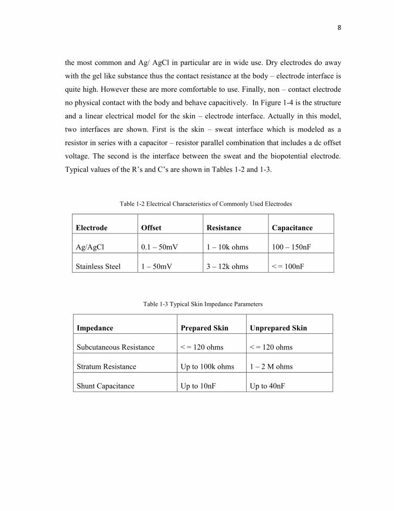


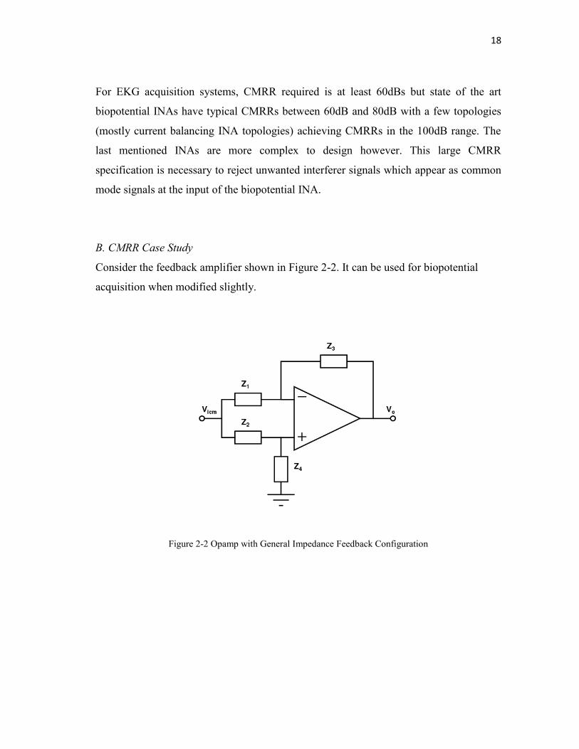


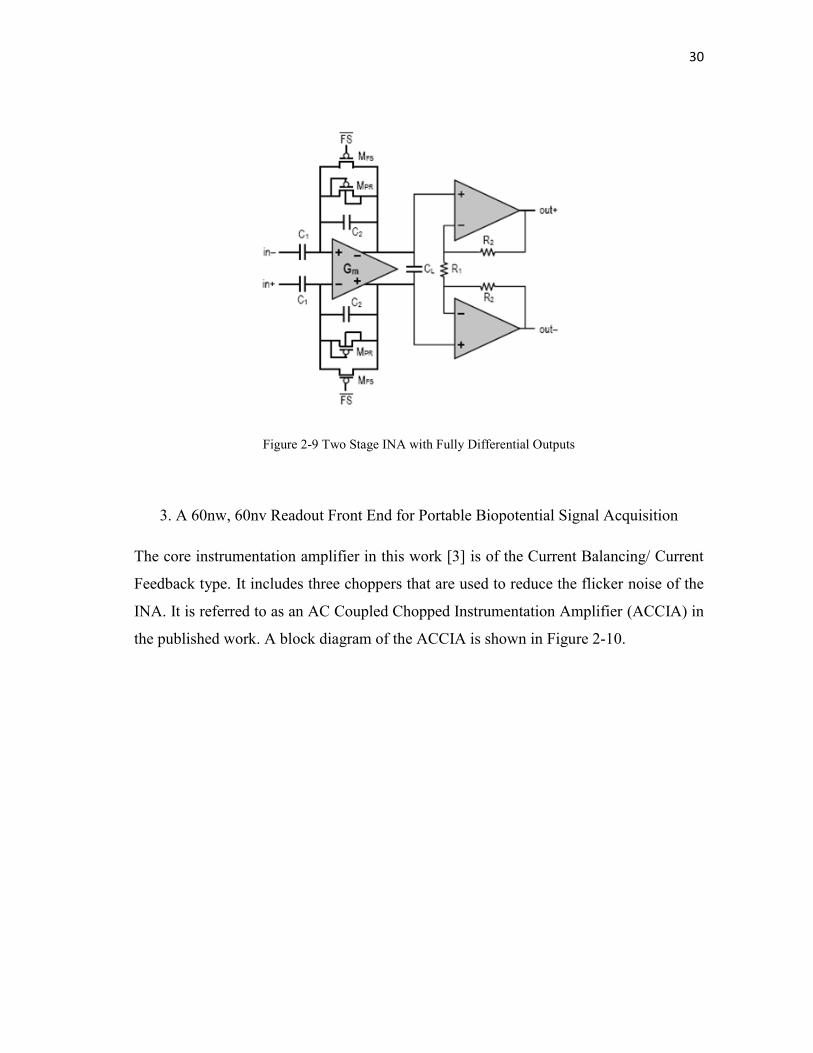


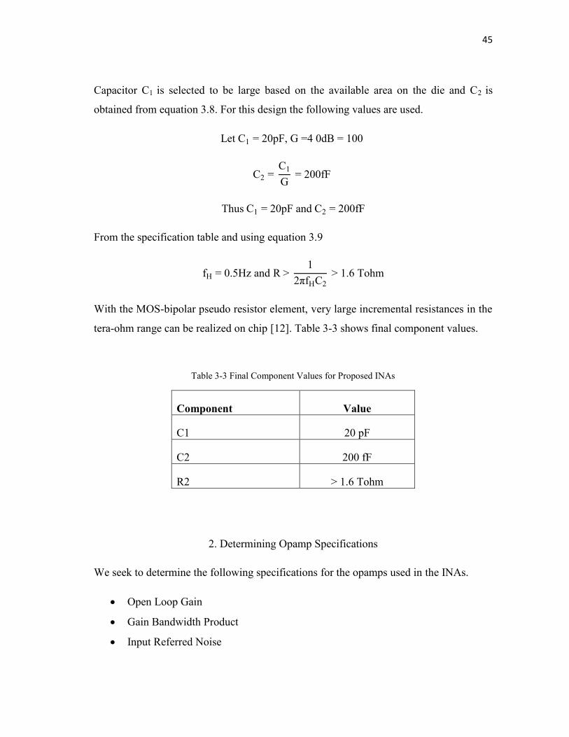


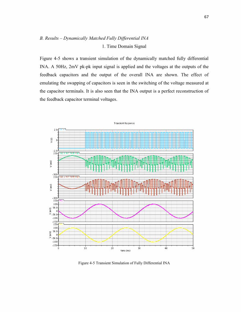

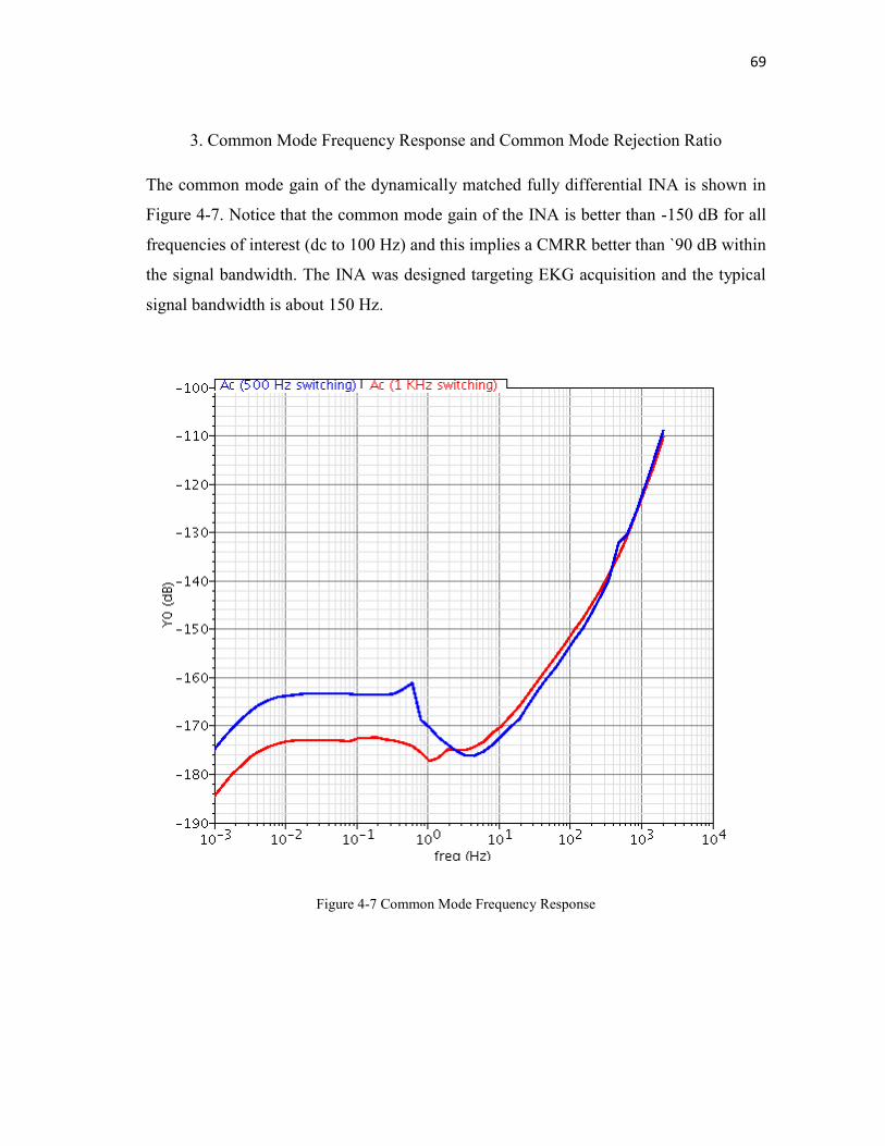


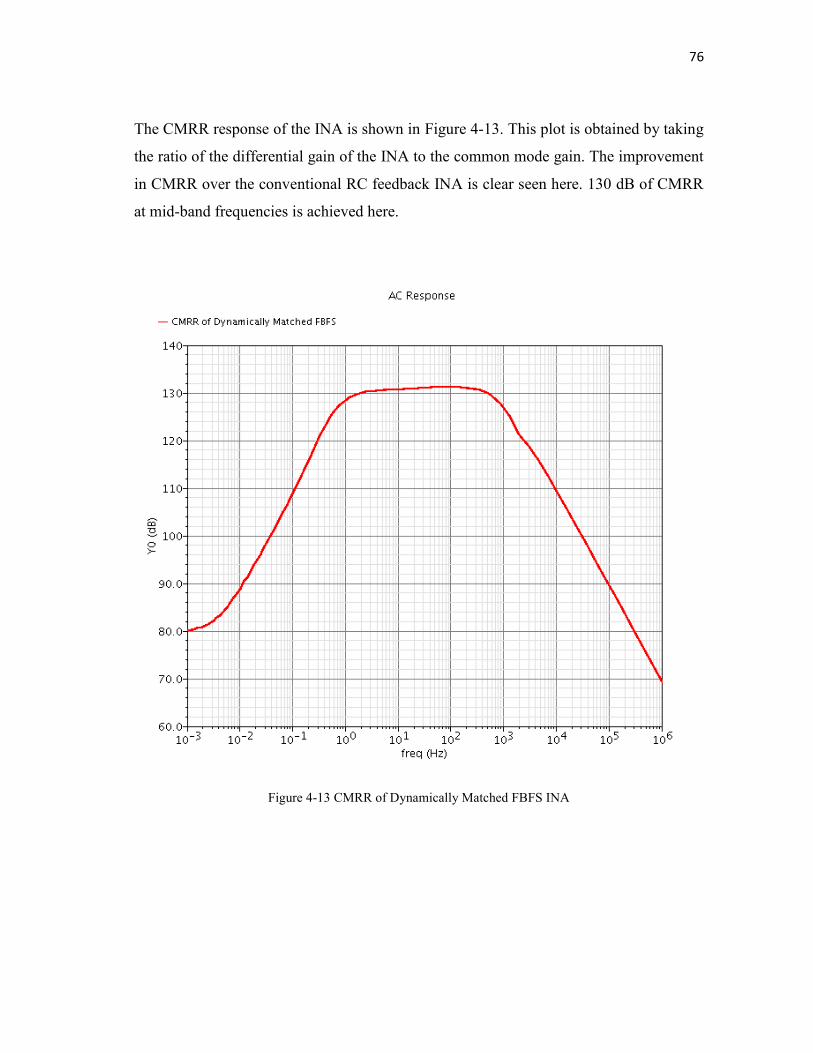


![High CMRR Voltage Mode Instrumentation Amplifier Using a New … · The schematic diagram of differential pair polarized by adaptive biasing circuit [14], [15] is presented in Fig.](https://static.documents.pub/doc/80x56/5f2e553dc424990ed836ab0c/high-cmrr-voltage-mode-instrumentation-amplifier-using-a-new-the-schematic-diagram.jpg)


