Thirteenth International Symposium on Space Terahertz Technology, Harvard University, March 2002. A Novel Full Waveguide Band Orthomode Transducer Gopal Narayanan l , and Neal R. Erickson Department of Astronomy University of Massachusetts Amherst, MA 01003 Abstract At millimeter and subrnillimeter wavelengths, cryogenically cooled receivers based on STS and HEB technologies are approaching the quantum limit in noise temperature. Further increase in sensitivity can be obtained by using dual-polarized operation. One of the principal components of a dual -polarization receiver is a polarization diplexer or orthomode transducer (0MT). Traditionally the OMT used in radio astronomy re- ceivers is the wire grid, which can be large and bulky. A waveguide based OMT, on the other hand, can be integrated with the mixer blocks and cryogenically cooled thereby reducing ohmic losses. A waveguide based OMT also lends itself well to integration into focal-plane array receivers. In this paper, we present the design of a novel OMT that can be constructed using conventional split-block techniques. The design is based on the proposed Bd)ifot OMT by Wollack [1], but has been considerably modified to (a) make it easy to fabricate, and (b) make it scalable to I THz. The return loss is —20 dB or better over a full waveguide-band (r- 40% bandwidth), and the cross- polarization and isolation are better than —70 dB. Design details of a W-band OMT are presented. 1 Introduction An orthomode transducer (OMT) is a device that separates orthogonal polarizations within the same frequency band. In the literature, OMT's are called by various other names such as polarization diplexers, dual-mode transducers, orthomode junctions or orthomode tees. With receiver noise temperatures of waveguide-based SIS and HEB mixers approaching a few times the quantum limit, further increase in sensitivity can be obtained using dual- polarized operation. In radio astronomical applications, the conventional way to separate orthogonal polarizations is the wire-grid diplexer, which is a quasi-optical device that con- sists of free-standing parallel wires. The polarization with the E-field parallel to the wires is reflected, while the component orthogonal to the wires is transmitted through. However, the wiregrid polarization diplexer is large and bulky. If we desire the mixers for both polariza- tions to reside in one cryostat, the wiregrid should preferentially be inside the dewar, which correspondingly increases the size of the required dewar. A broadband vvaveguide-based OMT would be a preferable alternative as it would much smaller, and it would be a good match to available high-performance dual-polarized broadband corrugated feedhorns. 'e-mail: gopal@ astro.umass.edu 505
Transcript
Thirteenth International Symposium on Space Terahertz Technology, Harvard University, March 2002.
A Novel Full Waveguide Band Orthomode Transducer
Gopal Narayanan l , and Neal R. Erickson
Department of AstronomyUniversity of Massachusetts
Amherst, MA 01003
Abstract
At millimeter and subrnillimeter wavelengths, cryogenically cooled receivers basedon STS and HEB technologies are approaching the quantum limit in noise temperature.Further increase in sensitivity can be obtained by using dual-polarized operation. Oneof the principal components of a dual -polarization receiver is a polarization diplexeror orthomode transducer (0MT). Traditionally the OMT used in radio astronomy re-ceivers is the wire grid, which can be large and bulky. A waveguide based OMT, on theother hand, can be integrated with the mixer blocks and cryogenically cooled therebyreducing ohmic losses. A waveguide based OMT also lends itself well to integrationinto focal-plane array receivers. In this paper, we present the design of a novel OMTthat can be constructed using conventional split-block techniques. The design is basedon the proposed Bd)ifot OMT by Wollack [1], but has been considerably modified to(a) make it easy to fabricate, and (b) make it scalable to I THz. The return lossis —20 dB or better over a full waveguide-band (r- 40% bandwidth), and the cross-polarization and isolation are better than —70 dB. Design details of a W-band OMTare presented.
1 Introduction
An orthomode transducer (OMT) is a device that separates orthogonal polarizations withinthe same frequency band. In the literature, OMT's are called by various other names suchas polarization diplexers, dual-mode transducers, orthomode junctions or orthomode tees.With receiver noise temperatures of waveguide-based SIS and HEB mixers approachinga few times the quantum limit, further increase in sensitivity can be obtained using dual-polarized operation. In radio astronomical applications, the conventional way to separateorthogonal polarizations is the wire-grid diplexer, which is a quasi-optical device that con-sists of free-standing parallel wires. The polarization with the E-field parallel to the wires isreflected, while the component orthogonal to the wires is transmitted through. However, thewiregrid polarization diplexer is large and bulky. If we desire the mixers for both polariza-tions to reside in one cryostat, the wiregrid should preferentially be inside the dewar, whichcorrespondingly increases the size of the required dewar. A broadband vvaveguide-basedOMT would be a preferable alternative as it would much smaller, and it would be a goodmatch to available high-performance dual-polarized broadband corrugated feedhorns.
'e-mail: gopal@ astro.umass.edu
505
Thirteenth International Symposium on Space Terahertz Technology, Harvard University, March 2002.
waveguide based OMT also lends itself well to integration into focal-plane array receivers.In this paper, we present the design of a full-waveguide band OMT for the W-band, whichis scalable to 1 THz.
2 General Considerations for OMTs
With improved fabrication techniques [2,3,4], high-quality waveguide blocks can be madeto 1 THz and beyond. One of the principal requirements in our design is the scalabilityof the design to terahertz frequencies. An OMT used for radio astronomy purposes shouldsatisfy several important requirements: (1) A return loss of EN., 20 dB or better for a fullwaveguide band 40% bandwidth). (2) Isolation between the two orthogonal polariza-tion ports of better than 40 dB. (3) Cross-polarization term should be less than 40 dB.Cross-polarization for a given polarization port is the amount of signal present from theorthogonal polarization. One of the driving goals of an OMT design should be that thecross-polarization introduced by the OMT should not exceed that produced by the opticsand feedhom that precede it in the system. (4) Low Insertion Loss. Since the OMT willbe operated cryogenically the ohmic losses are less important that for room temperatureoperation. (5) The design should be scalable to 1 THz. The fabrication of the OMT shouldlend itself to established split-block techniques.
For any waveguide device, the broadband operation of the device is tied to its symme-try properties. Symmetrical or non-symmetrical transitions in waveguides produce higherorder modes. Most of the higher modes are evanescent and do not propagate. However,uncompensated higher order modes store reactive energy which prevents the broadbandoperation of the device. What sorts of higher order modes are produced often dictatesthe broadband isolation and input match of waveguide devices. To design a broadbanddevice, it is necessary to design the transitions such that only even-order higher modesare produced, because they are easier to compensate. A waveguide device is defined assymmetrical if different transitions cause the dominant mode to only generate symmetrical(even-order) higher modes. A device is defined as non-symmetrical if the dominant mode,in addition produces odd-symmetrical higher order modes.
Boifot classified waveguide-based OMTs into three groups [5,6] based on their in-creasing symmetry. Class I represents the simplest and most common approach, with onemain arm for one mode and one orthogonal sidearm for the other mode. The Main armmode is symmetric while the sidearm mode is not. An example of such an OMT is thatused in [7], where the H-bend in the sidearm breaks its symmetry, resulting in narrowerpercentage bandwidth (— 20%). The Class II configuration OMT is more complex. Herethere is one main arm, but the side arm is split into two symmetrical parts from the mainarm. An example of this sort of device is that presented in [5] and implemented by Wol-lack [1]. In this device, the main arm mode sees a symmetrical device as in the Class Iequivalent. In addition, the side arm also sees symmetrical splitting and combining junc-tions. The symmetrical nature of this splitting and combining makes it possible to achievea good broadband match even for the side arm mode. The Class III OMTs are even more
506
Thirteenth International Symposium on Space Terahertz Technology, Harvard University, March 2002.
complex, with both the main and side arms split into two symmetrical parts. The split-ting junction essentially forms a classic turnstile junction whose matching properties havebeen well studied [8]. Since the splitting junction is symmetric both in the main and sidearms, higher order symmetric modes will naturally be canceled in both arms, and thus theseOMTs should have a natural broadbanded match and isolation performance. However, thisclass of OMT is very complex and hence expensive to fabricate.
Figure 1: (a) The six-port Classic Turnstile Junction. A and B denote the two ports at theinput for the orthogonal polarization. (b) Folded Turnstile Junction, which becomes a ClassII OMT. Ports Al and A2 are folded together.
The Boifot junction [5] is a Class II OMT, but it can be thought of as a turnstile junc-tion where two of the ports have been folded parallel to the common port (see Figure 1).The two ports that form the main arm are separated by a metal septum, recombined intosquare waveguide and then transformed into a standard full-height waveguide. The twosymmetric side arms remain the same as in the Class III turnstile-type OMT. For the po-larization meant for the side arms, the septum can be thought of as back-to-back "mitered"bends which feeds the symmetric side arm ports. A WR-42 OMT based on the BQifot de-sign was made and tested by Wollack [1]. In BQifot's design, pins are placed at the entranceapertures of the side arms. There are a pair of such pins for each sidearm. These pins act ascapacitive posts. From the perspective of the main arm, these pins tune out the discontinu-ity of the holes created by the side arms in the main waveguide. From the perspective of theside arms, these pins along with the shape of the septum serve to tune out the dispersive re-flective termination that is created by the septum in the main arm. While the pins providedadequate match for the OMT, their small diameters (0.127 ram for the 3 mm band) and thecomplexity of assembly of the pins in the block make them unsuitable for scaling the OMTto terahertz frequencies. In this work, we replaced the pins with capacitive steps at the sidearm apertures (see Figure 1) which are easy to fabricate in-situ with the waveguide block,and work as effectively as the pins do.
507
Thirteenth International Symposium on Space Terahertz Technology, Harvard University, March 2002.
3 OMT Design
3.1 Design Methods
Most parts of the OMT design was carried out using CST Microwave Studio (CST MWS)[9]. CST MWS is based on the finite integration (Fl) method, which is a one-to-one trans-lation of Maxwell's equations into a discrete space formulation without simplification orspecialization. As a general approach its theoretical framework has been developed by thelikes of particle accelerator designers for over three decades, and hence is a robust designtool. The FT method works explicitly in the time domain, and hence a full broadband simu-lation can be performed in one single solver run. MWS is well suited for electrically largestructures and features a powerful, parametric drawing editor to lay out the structures. Italso comes with a built-in optimizer which was used heavily to optimize the geometry ofthe septum and the dimensions of the capacitive waveguide steps. While most of the designwas carried out in CST MWS, some critical portions such as the junction part of the OMTwere also simulated with Agilent's HFSS [10]. The HFSS results verified the predictionsof CST MWS, and hence the final results and optimizations were derived using the latter.
3.2 OMT Junction
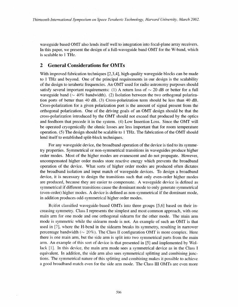
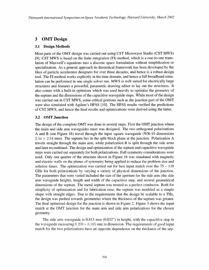
The design of the complete OMT was done in several steps. First the OMT junction wherethe main and side arm waveguides meet was designed. The two orthogonal polarizationsA and B (see Figure lb) travel through the input square waveguide (WR-10 dimensions2.54 x 2.54 mm). The septum lies in the split block plane at the junction. Polarization Atravels straight through the main arm, while polarization B is split through the side armsand later recombined. The design and optimization of the septum and capacitive waveguidesteps were carried out separately for both polarizations. Full symmetry considerations wereused. Only one quarter of the structure shown in Figure lb was simulated with magneticand electric walls on the planes of symmetry being applied to reduce the problem size andsolution times. The optimization was carried out for best input match over the 75 — 110GHz for both polarizations by varying a variety of physical dimensions of the junction.The parameters that were varied included the size of the aperture for the side arm (the sidearm waveguide height), length and width of the capacitive step, and several geometricaldimensions of the septum. The metal septum was treated as a perfect conductor. Both forsimplicity of optimization and for fabrication ease, the septum was modeled as a simpleshape with straight edges. Due to the requirements that the design be scalable to a THz,the design was pushed towards geometries where the thickness of the septum was greater.The final optimized design for the junction is shown in Figure 2. Figure 3 shows the inputmatch at the OMT junction for the main arm and side arm polarizations for the chosengeometry.
The side arm waveguide is 0.813 mm (0.032") in height, with the capacitive step inthe waveguide measuring 0.208 x 0.165 mm in dimension. The requirements of good inputmatch for the two polarizations have an opposite dependence on the thickness of the sep-
508
1-1-0.508
Thirteenth International Symposium on Space Terahertz Technology, Harvard University, March 2002.
Figure 2: (a) Split-block view of the optimized OMT junction. All dimensions are inmillimeters. (b) View of the Septum with some relevant dimensions. The septum is 0.254mm thick for the W-band OMT.
turn. The bandwidth of good match for the side arm polarization (polarization B) increaseswith increasing septum thickness. For this polarization, increasing septum thickness makesthe septum look more and more like back-to-back mitered bends. For the main arm (po-larization A), the bandwidth of good match reduces with increasing septum width. A thinseptum produces less discontinuity than a thick septum. The dimensions and geometry ofthe capacitive step acts as an additional variable in adjusting the match. The optimal thick-ness of 0.254 mm chosen here for the septum represents a good compromise for the twopolarizations, while still remaining an easy enough junction to fabricate.
3.3 E-Plane Bend Across Split Block
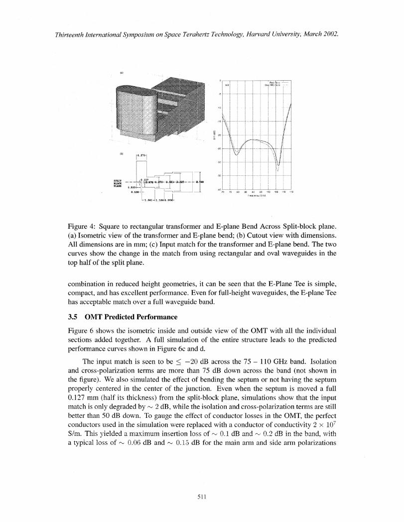
In the main arm, polarization A travels through the 1:1 square waveguide and is then trans-formed into a full-height rectangular waveguide. The transformer is followed by an E-planebend across the split-block to bring the port out orthogonal to the side-arm port. The squareto rectangular transition is accomplished using a 3-section transformer. The transformer isimmediately followed by the E-plane bend. The bend itself consists of two steps, both be-low the split block plane (see Figure 4). In the top block of the split-plane, a full-heightrectangular waveguide brings out the main arm port to the outside world. The rectangularwaveguide in the top block is hard to machine (it would have to be punched or fabricatedas a cylindrical insert and pressed and soldered prior to milling the rest of the features inthe top half). In view of this, we designed an oval waveguide which can be directly ma-chined with an end-mill. The oval waveguide uses full-radius corners (0.635 mm), andhas a = 2.79 mm (10% increased). Figure 4c shows that the reduction in bandwidth ofmatch for using oval waveguide is minimal. The distance from the OMT junction shownin Figure 2 and the transformer E-plane bend shown of Figure 4 is 0.94 mm. This distance
509
Thirteenth International Symposium on Space Terahertz Technology, Harvard University, March 2002.
75 80 85 90 95 100 105 110 115Frequency (GHz)
Figure 3: Input match (S11) in dB for the polarizations in the main and side arms for theOMT junction. The side arms match is worse because the side arm sees less symmetry thanthe main arm. Nevertheless, between 75 — 110 GHz, the match is seen to be at least as goodas the required 20 dB.
was optimized in a linear circuit simulator [11] by using ideal rectangular waveguide trans-mission line sections between the de-embedded S-parameter equivalent networks from theOMT-junction and the transformer section.
3.4 E-Plane Combiner for Side Arm
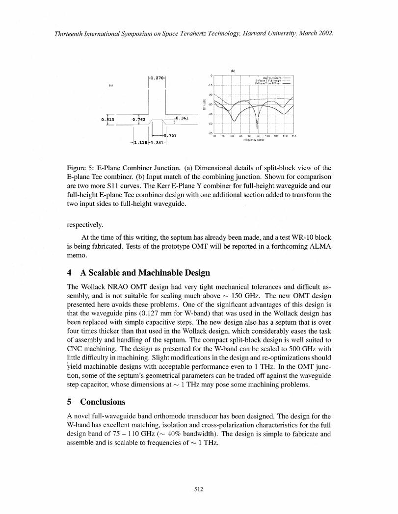
The two side arms are made to bend around the main arm features through a pair of E-planebends and are then recombined into a full-height rectangular waveguide which emerges onthe opposite side of the square input waveguide of the block. A full-height to full-heightwaveguide E-plane power divider/combiner design has been recently presented by Kerr[12]. In the Kerr design, the two incoming ft-ill-height rectangular waveguides meet in asquare waveguide section which is then transformed back into rectangular waveguide. Theresulting combiner is physically quite long (, 8 mm for W-band). We designed a very sim-ple power combiner with excellent performance across a full waveguide band to combinetwo side arm waveguides (with a height of 0.813 mm each) to full-height waveguide. Thiscombiner has the advantage that its length is quite small (2.54 mm). Figure 5 shows thecross-sectional view of the resulting combiner and its predicted performance.
At the junction of the combiner, the two waveguide arms are a little over half-height(0.762 mm high). There is a broad pedestal in the middle of the combining junction. Sur-prisingly in this reduced height guide, such a simplified geometry works as well as the morecomplex E-Plane Y junction shown in [12]. This combining junction, which can be thoughtof as an E-Plane Tee power divider can also be used for power division or combining forfull-height to full-height waveguides. In Figure 5b, the input match for our E-Plane Teepower combiner is compared against the full-height Kerr Y combiner, and a slightly mod-ified version of the E-Plane Tee combiner for full-height waveguide. Especially for power
510
(b) 2701
SPLITBLOCK
0 .535
0 .158—
641--- 1 . 184-11 . 06411--
85 90 100 105Frequercy (0,1z)
10
Thirteenth International Symposium on Space Terahertz Technology, Harvard University, March 2002.
Figure 4: Square to rectangular transformer and E-plane Bend Across Split-block plane.(a) Isometric view of the transformer and E-plane bend; (b) Cutout view with dimensions.All dimensions are in mm; (c) Input match for the transformer and E-plane bend. The twocurves show the change in the match from using rectangular and oval waveguides in thetop half of the split plane.
combination in reduced height geometries, it can be seen that the E-Plane Tee is simple,compact, and has excellent performance. Even for full-height waveguides, the E-plane Teehas acceptable match over a full waveguide band.
3.5 OMT Predicted Performance
Figure 6 shows the isometric inside and outside view of the OMT with all the individualsections added together. A full simulation of the entire structure leads to the predictedperformance curves shown in Figure 6c and d.
The input match is seen to be < —20 dB across the 75 — 110 GHz band. Isolationand cross-polarization terms are more than 75 dB down across the band (not shown inthe figure). We also simulated the effect of bending the septum or not having the septumproperly centered in the center of the junction. Even when the septum is moved a full0.127 mm (half its thickness) from the split-block plane, simulations show that the inputmatch is only degraded by — 2 dB, while the isolation and cross-polarization terms are stillbetter than 50 dB down. To gauge the effect of conductor losses in the OMT, the perfectconductors used in the simulation were replaced with a conductor of conductivity 2 x 10⁷S/m. This yielded a maximum insertion loss of 0.1 dB and 0.2 dB in the band, witha typical loss of --, 0.06 dB and 0.15 dB for the main arm and side arm polarizations
511
(a)
0.813 0.762
1.118
1.270—
. 757
1.341-1
Kerr E-Plane Y - - - -
Ft,;r. T, t, al? MITI -
E-Plane I Full-Height -- ......
1;I 1
iIi :
!;
:
A ! ; 1i ! 1 1 i !
i I 1 g - ii i I;
;
I I
SO70 75 BO 85 90 95 ' 00 105 110 115
Frequency (Cril-i,)
0
-20
-30
Thirteenth International Symposium on Space Terahertz Technology, Harvard University, March 2002.
Figure 5: E-Plane Combiner Junction. (a) Dimensional details of split-block view of theE-plane Tee combiner. (b) Input match of the combining junction. Shown for comparisonare two more Sll curves. The Kerr E-Plane Y combiner for full-height waveguide and ourfull-height E-plane Tee combiner design with one additional section added to transform thetwo input sides to full height waveguide.
respectively.
At the time of this writing, the septum has already been made, and a test WR-10 blockis being fabricated. Tests of the prototype OMT will be reported in a forthcoming ALMAmemo.
4 A Scalable and Machinable Design
The Wollack NRAO OMT design had very tight mechanical tolerances and difficult as-sembly, and is not suitable for scaling much above 150 GHz. The new OMT designpresented here avoids these problems. One of the significant advantages of this design isthat the waveguide pins (0.127 mm for W-band) that was used in the Wollack design hasbeen replaced with simple capacitive steps. The new design also has a septum that is overfour times thicker than that used in the Wollack design, which considerably eases the taskof assembly and handling of the septum. The compact split-block design is well suited toCNC machining. The design as presented for the W-band can be scaled to 500 GHz withlittle difficulty in machining. Slight modifications in the design and re-optimizations shouldyield machinable designs with acceptable performance even to 1 THz. In the OMT junc-tion, some of the septum's geometrical parameters can be traded off against the waveguidestep capacitor, whose dimensions at 1 THz may pose some machining problems.
5 Conclusions
.. ■ !
A novel full-waveguide band orthomode transducer has been designed. The design for theW-band has excellent matching, isolation and cross-polarization characteristics for the fulldesign band of 75 — 110 GHz (— 40% bandwidth). The design is simple to fabricate andassemble and is scalable to frequencies of — 1 THz.
512
Thirteenth international Symposium on Space Terahertz Technology, Harvard University, March 2002.
Research at the Five College Radio Astronomy Observatory is funded in part by agrant from the National Science Foundation.
6 References
[1] E. Wollack, "A Full Waveguide Band Orthomode Junction", Electronics DivisionInternal Report, National Radio Astronomy Observatory, Green Bank, WV, no. 303,May 1996.
[2] G. Narayanan, N. R. Erickson, and R. M. Grosslein, "Low Cost Direct Machining ofTerahertz waveguide Structures," Tenth International Symposium on Space TerahertzTechnology, pp. 518-528, Mar, 99.
[3] C. K. Walker, G. Narayanan, A. Hungerford, T. Bloomstein, S. Palmacci, M. Stern,J. Curtin, J., "Laser Micromachining of Silicon: A New Technique for Fabricat-ing TeraHertz Imaging Arrays", Astronomical Telescopes and Instrumentation, SPIESymposium, Kona, Hawaii, 1998.
[4] C. K. Walker, G. Narayanan, T. M. Bloomstein, "Laser Micromachining of Silicon:A New Technique for Fabricating Terahertz Waveguide Components", 1997, 8th In-ternational Symposium on Space Terahertz Technology, eds. Blundell and Tong,Harvard University.
[5] BOifot, A. M., Lier, E., and Schaug-Pettersen, T., "Simple And Broadband Ortho-mode Transducer", 1990, Proc. IEE, vol. 137, no. 6, pp 396-400.
[6] Bpifot, A. M., "Classification of Orthomode Transducers", 1991, European Transac-tions on Telecommunication and Related Technologies, vol 2, no. 5, pp 503-510.
[7] Chattopadhyay, G., Philhour, B., Carlstrom, J. E., Church, S. Lange, A., and Zmuidz-inas, J., "A 96 GHz Orthomode Transducer For Polatron", 1998, IEEE Microwaveand Guided Wave Letters, vol 8., no. 12, pp 421-423.
[8] Montgomery, C. G., Dicke, R. H., and Purcell, E. M., "Principles of MicrowaveCircuits", Dover Publications, New York, 1948, pp. 459-466.
[10] High Frequency Structure Simulator (HFSS), v 5.6, Agilent Technology Inc., PaloAlto, CA.
[11] Advanced Design System (ADS), v2001, Agilent Technology Inc., Palo Alto, CA.
[12] Kerr, A. R., "Elements for E-Plane Split-Block Waveguide Circuits", 2001, ALMAMemo Series No. 381, NRAO.
513
70 75 80 85 90 25 100 105 110 115Frequence (G Hz)
100 1 05 110 11570 75 80 85 90 95Frequence (G Hz)
(c) Main Arm Port
(d) Side Arm Port
10
-10
-20
-30
-50
10
-10
-20
-30
-40
-50
511 (dB)Insertion Loss (dB)
- - - t - - - -
(b)
Thirteenth International Symposium on Space Terahertz Technology, Harvard University, March 2002.
Figure 6: The full Orthomode Transducer. (a) Isometric view from the outside. The waveg-uide features of the OMT block measure 13.2 x 7.6 x 2.54 mm. (b) Inside view showingthe septum resting in the split block plane. (c) Simulated performance for the full structurefor the main arm polarization. (d) Same as (c) for the side arm polarization port.