The author hereby grants to M.I.T. permission to reproduce and distribute publiclypaper and electronic copies of this thesis and to grant others the right to do so.
A uthor ........................ . ........... ... ..............................Department of Electrial Engineering and Computer Science
April 1, 1998
Approved by ............
Technical Supervisor, Draper Laboratory
Certified by ............... ............ ......... . .... ........................ .Bernard C. Lesieutre
Assistant Professor of Electrical EngineeringThe~ S Supervisor
A A, c epted by .................. .... :. ......... ..... ...........Arthur C. Smith
Chairman, Department Committee on Graduate Theses
A Regulated, Charge-Pump CMOS DC/DC Converterfor Low-Power Applications
by
Jooyoun Park
Submitted to the Department of Electrical Engineering and Computer Scienceon April 1, 1998, in partial fulfillment of the requirements for the degree of
Master of Engineering in Electrical Engineering and Computer Science
Abstract
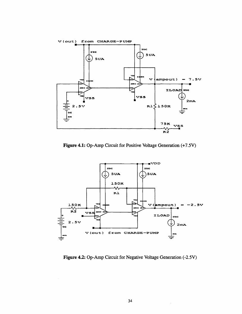
A regulated, low-power charge-pump DC/DC converter implemented in CMOS technol-ogy has been designed and extensively simulated in HSPICE. The charge-pump circuit isable to generate both positive and negative voltages. The converter consists of a charge-pump circuit operated at 500kHz from a +5V supply and a pair of op-amps which functionas the regulation mechanism. The desired output voltages, +7.5V and -2.5V, are generatedby the op-amps where the charge-pump supplies the rail voltages beyond the nominal Vzsof OV and the nominal VDD of +5V. Given a 2mA load, the target output voltages of -2.5Vand +7.5V are reached to within 1 mV, with an output ripple < 2mV. The efficiency of theconverter pair is 51%.
Thesis Supervisor: Bernard C. Lesieutre, Ph.D.Title: Assistant Professor of Electrical Engineering
Acknowledgments
This thesis would not have been possible without the encouragement, support andtechnical guidance of several people at Draper Laboratory and at MIT.
At Draper, I would like to thank my technical supervisor, Ralph Haley, whose encourage-ment and saintly patience motivated me to continue my work until the end. I am alsoindebted to Paul Ward, Robert Jurgilewicz, Thomas King, and Shida Martinez, whosetechnical expertise and guidance have been invaluable.
At MIT, I would like to thank Dr. David Perreault and my thesis advisor, ProfessorBernard Lesieutre, who were instrumental in helping me formulate the theoreticalbackbone of my thesis.
I would also like to thank my parents and my friends who have been very generous withtheir support and encouragement throughout my 5-year stay at MIT.
This thesis was prepared at The Charles Stark Draper Laboratory, Inc.,312.
Publication of this thesis does not constitute approval by Draper or theof the findings or conclusions contained herein. It is published forstimulation of ideas.
under Draper CSR
sponsoring agencythe exchange and
Permission is hereby granted by the author, to the Massachusetts Institute of Technologyto reproduce any or all of this thesis.
/Jooyoun Park
ASSIGNMENT
Draper Laboratory Report Number T-1303
In consideration for the research opportunity and permission to prepare my thesis by andat The Charles Stark Draper Laboratory, Inc., I hereby assign my copyright of the thesis toThe Charles Stark Draper Laboratory, Inc., Cambridge, Massachusetts.
/Jooyoun Park Date__ __
Table of Contents
1 Introduction ................................................. ...................................................... 131.1 The Need for On-Chip Power Converters ...................................... .... 131.2 Motivation for a Regulated CMOS Charge-Pump DC-DC Converter ............ 141.3 O utline of Thesis ................................................................... ....................... 15
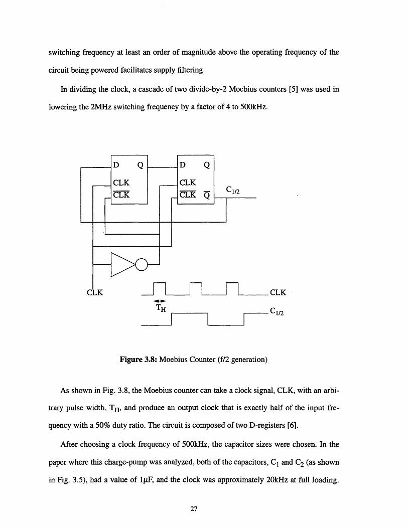
3 Voltage Generation: A CMOS Charge-Pump.......................... .................... 193.1 Overview of Charge-Pump Circuits..............................193.2 Description of Charge-Pump Circuit Under Study .......................................... 19
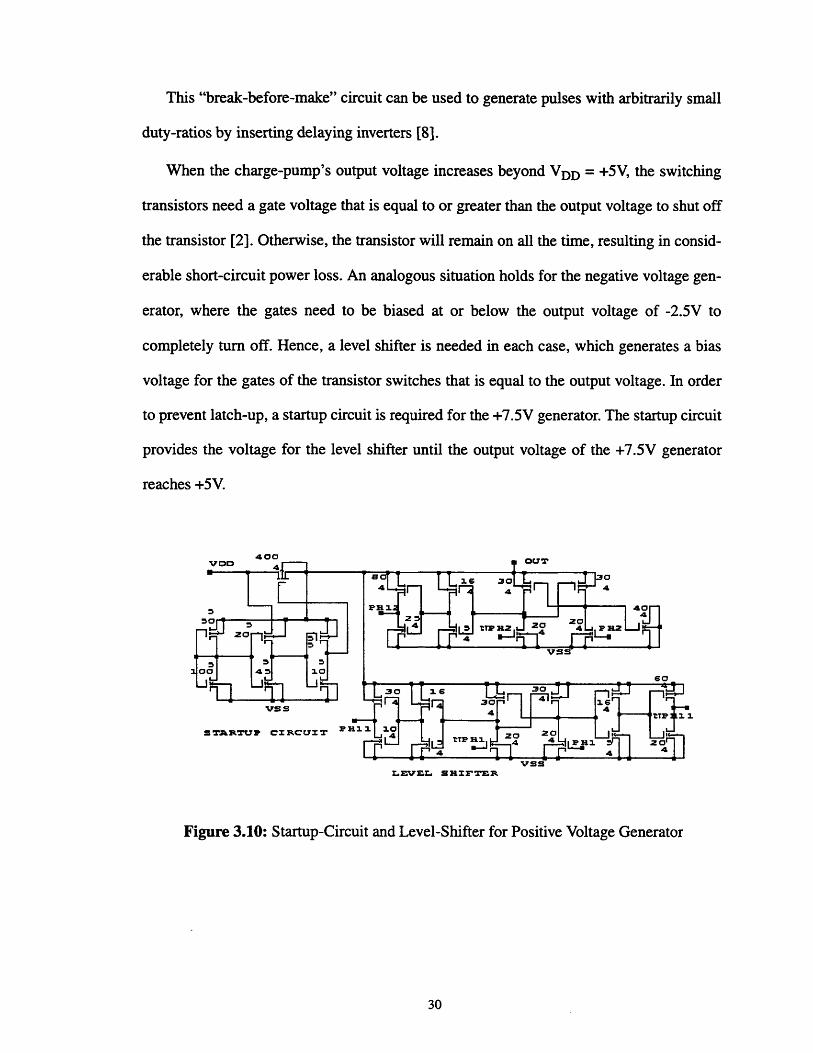
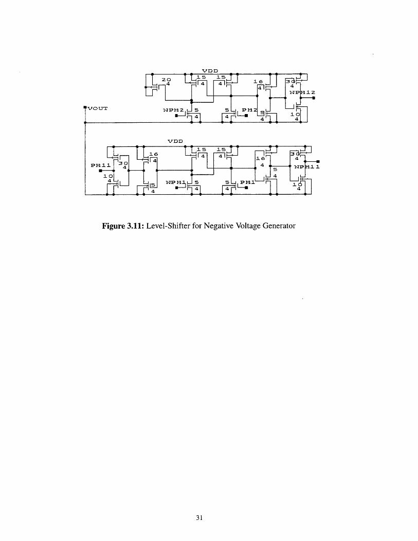
3.2.1 Operation of the Charge-Pump ................................................... 213.2.2 Dynamic (Transient) Response .................................................... 223.2.3 Clock Speed and Capacitors ................................................ 263.2.4 Switch Resistances .............................. ........ ............. 293.2.5 Auxiliary Circuits Required for Operation of the Charge-Pump ..... 29
4.4.1 Simulations Under Nominal Conditions ......................................... 414.4.2 Power Supply Rejection Simulation ....................................... 474.4.3 Load Regulation Simulations ....................................... ..... 494.4.4 Summary of Transient Response Results ...................................... 52
5 Other Output Regulation Schemes................................................535.1 Pulse W idth M odulation ...................................... ................ 535.2 Pulse Frequency M odulation ..................................... ............. 56
Figure 3.1: Positive Voltage Generator .................................. 20Figure 3.2: Negative Voltage Generator .......................................... ....................... 20Figure 3.3: The Two Switching Phases of Positive Voltage Generation.....................21Figure 3.4: The Two Switching Phases of Negative Voltage Generation ...................21Figure 3.5: Positive Voltage Generator Used in Deriving the Average Equations ........22Figure 3.6: Transient Response of Charge-Pump: <VC2> = VOUT - VDD ..................... 25Figure 3.7: Bode Plot of <VC2>: VOUT-VDD ................................... ..................... 26Figure 3.8: Moebius Counter (f/2 generation) ................... .......... 27Figure 3.9: Break-Before-Make Circuit..............................................29Figure 3.10: Startup-Circuit and Level-Shifter for Positive Voltage Generator ..........30Figure 3.11: Level-Shifter for Negative Voltage Generator......................................... 31Figure 4.1: Op-Amp Circuit for Positive Voltage Generation (+7.5V) .......................34Figure 4.2: Op-Amp Circuit for Negative Voltage Generation (-2.5V) ......................34Figure 4.3: Test Circuit Used in Simulation of PSR for +7.5V Generator.....................35Figure 4.4: Test Circuit Used in Simulation of PSR for -2.5V Generator......................36Figure 4.5: Estimated Power Supply Rejection: +7.5V Generator ..............37Figure 4.6: Estimated Power Supply Rejection: -2.5V Generator................................37Figure 4.7: Test Circuit for Simulating Load Regulation +7.5V..................................38Figure 4.8: Test Circuit for Simulating Load Regulation: -2.5V.............................. 39Figure 4.9: Estimated Effect of Load Variations on +7.5V Generator Output...............39Figure 4.10: Estimated Effect of Load Variations on -2.5V Generator Output...........40Figure 4.11: Complete Converter/Regulator Circuit for +7.5V Generation ...................42Figure 4.12: Complete Converter/Regulator Circuit for -2.5V Generation....................43Figure 4.13: +7.5V Regulator Simulation: Nominal Conditions ....................................44Figure 4.14: Steady-State Voltages and Currents for Fig. 4.13 ...................................44Figure 4.15: -2.5V Regulator Simulation: Nominal Conditions ..................................45Figure 4.16: Steady-State Voltages and Currents for Fig. 4.15 ...................................45Figure 4.17: +7.5V Regulator Simulation: Power Supply Rejection .............................47Figure 4.18: Steady-State Voltages and Currents for Fig. 4.17 ...................................48Figure 4.19: -2.5V Regulator Simulation: Power Supply Rejection ...........................48Figure 4.20: Steady-State Voltages and Currents for Fig. 4.19...................... 49Figure 4.21: +7.5V Regulator Simulation: Load Regulation..................50Figure 4.22: Steady-State Voltages and Currents for Fig. 4.21 ......................................50Figure 4.23: -2.5V Regulator Simulation: Load Regulation........................................ 51Figure 4.24: Steady-State Voltages and Currents for Fig. 4.23 ...................................51Figure 5.1: Block Diagram for PWM-Controlled Charge-Pump.................53Figure 5.2: Block Diagram for PFM-Controlled Charge-Pump ..................................56
10
List of Tables
Table 2.1: Design Specifications ........................................ 17Table 4.1: Comparison of Transient Measurements and Specifications .......................52
12
Chapter 1
Introduction
1.1 The Need for On-Chip Power Converters
The demand for low-power applications and the proliferation of battery-powered devices
have resulted in a steady decrease in the supply voltages of integrated circuits (ICs). The
power savings that result from a decrease in the supply voltage has been one of the prime
motivators for current research efforts which focus on the development of circuit topolo-
gies that can operate with 1.2V or lower supplies.
There is, however, a limit to which supply voltages can be lowered before performance
is adversely affected, particularly in analog designs. Care must be taken such that an
across-the-board lowering of the voltages will not result in some subcircuit being placed
out of its range of functionality. In mixed-signal IC's, for example, where analog and digi-
tal circuits coexist on the same substrate, the problem of circuits requiring different oper-
ating voltages emerges: digital circuits can often operate at lower voltages than analog
circuits. A similar situation arises in any chip where all of the subcircuits do not share the
same minimum operating voltage. In such ICs how does one minimize power consump-
tion?
One idea is to power the chip with several supply levels. This will decrease the aggre-
gate power consumption; however, the cost of manufacturing a product which incorpo-
rates such a chip will increase since several external supplies will be required. The current
trend in chip design is to move away from multiple supplies in favor of one. Given one low
voltage supply, how does one generate the requisite voltages for all the different subcir-
cuits? One solution, which will be explored in this thesis, is to use on-chip DC-DC con-
verters.
As more functional subcircuits are integrated on a single chip, and as devices become
smaller and more densely packaged, on-chip power converters will become increasingly
necessary. A piece of consumer electronics currently in development that addresses the
issue of integrating multiple supply rails on-chip is the InfoPad terminal being developed
at the University of California at Berkeley. The InfoPad is a hand-held personal communi-
cation system whose electronics require the generation of +5V, -17V, +12V and +1.5V, all
from a single 6V battery. This battery is responsible for powering the baseband circuitry,
the encoder/decoders for data compression, the A/D and D/A converters, the spreader and
despreader for spread spectrum RF communication, the RF transceiver, and the flat-panel
display [1].
1.2 Motivation for a Regulated CMOS Charge-Pump DC-DC ConverterIn lowering manufacturing costs and making devices lightweight, an on-chip DC-DC con-
verter is preferable to one that is off-chip. Discrete off-chip components tend to add to the
cost, size and weight of a device. Among the currently available IC processes, the imple-
mentation of a DC-DC converter in CMOS is desirable since CMOS is currently the tech-
nology of choice for low-power design. The popularity of CMOS is largely due to the ease
in designing circuits with minimal static power dissipation. In the interest of minimizing
size and cost, the DC-DC converter presented in this thesis will not make use of off-chip
magnetic elements such as inductors or transformers. Instead, off-chip capacitors will con-
stitute the only external elements. A charge-pump, which requires only capacitors and
integrated switches, will thus be used as the primary voltage conversion mechanism.
In order for the charge-pump to function as a voltage regulator, the circuit must be
controlled by a feedback mechanism. The regulation scheme that will be featured in this
thesis will be one that takes advantage of the regulation capabilities of an op-amp. Other
control schemes exist such as linear feedback regulation; the research group that supports
this thesis has implemented a working, charge-pump converter that is controlled by a lin-
ear regulator. This thesis will also discuss Pulse-Width Modulation (PWM) and Pulse-Fre-
quency Modulation (PFM) as alternative control schemes that can be used for applications
with design specifications different from that of the converter featured in this thesis.
1.3 Outline of Thesis
The following is a list of topics presented in this thesis:
* Chapter 2 discusses the specifications of the converter.* Chapter 3 features an analysis of the charge-pump.* Chapter 4 features an analysis of the Op-Amp regulator, along with simulation
results of the complete charge-pump/regulator circuit.* Chapter 5 discusses PWM and PFM as alternative control schemes.* Chapter 6 is the conclusion.
16
Chapter 2
Design Specifications and Methods
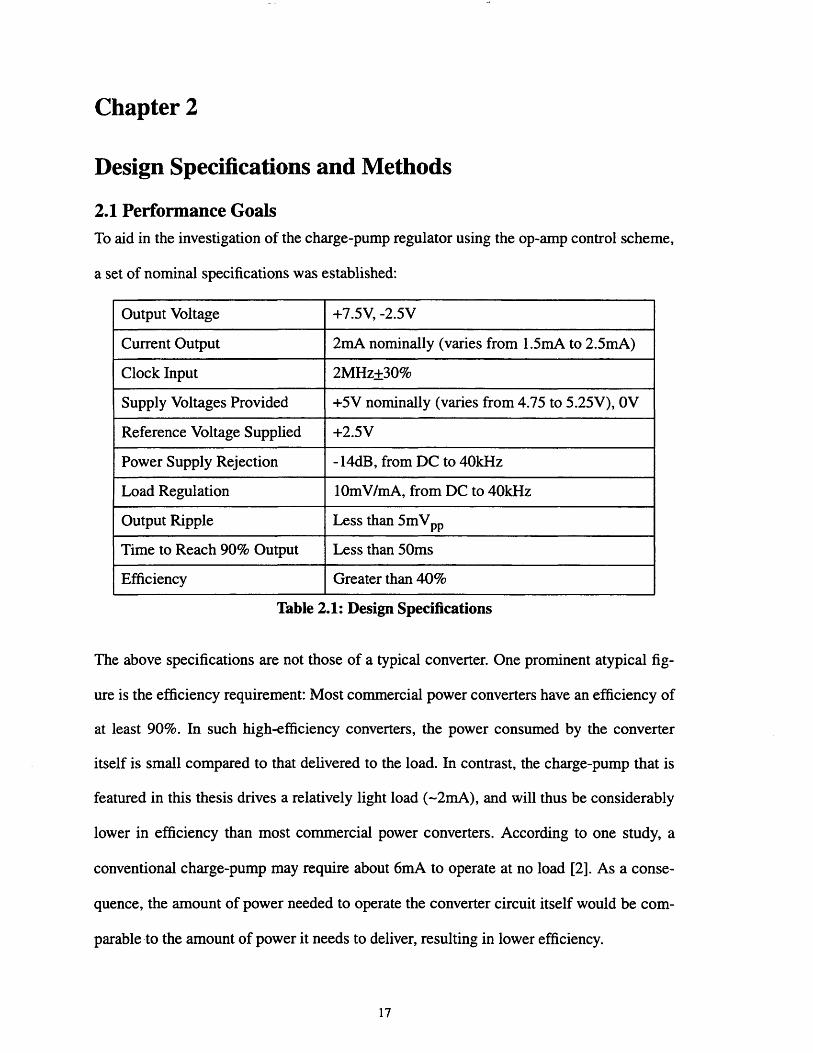
2.1 Performance GoalsTo aid in the investigation of the charge-pump regulator using the op-amp control scheme,
a set of nominal specifications was established:
Output Voltage +7.5V, -2.5V
Current Output 2mA nominally (varies from 1.5mA to 2.5mA)
Clock Input 2MHz+30%
Supply Voltages Provided +5V nominally (varies from 4.75 to 5.25V), OV
Reference Voltage Supplied +2.5V
Power Supply Rejection -14dB, from DC to 40kHz
Load Regulation 10mV/mA, from DC to 40kHz
Output Ripple Less than 5mVpp
Time to Reach 90% Output Less than 50ms
Efficiency Greater than 40%
Table 2.1: Design Specifications
The above specifications are not those of a typical converter. One prominent atypical fig-
ure is the efficiency requirement: Most commercial power converters have an efficiency of
at least 90%. In such high-efficiency converters, the power consumed by the converter
itself is small compared to that delivered to the load. In contrast, the charge-pump that is
featured in this thesis drives a relatively light load (-2mA), and will thus be considerably
lower in efficiency than most commercial power converters. According to one study, a
conventional charge-pump may require about 6mA to operate at no load [2]. As a conse-
quence, the amount of power needed to operate the converter circuit itself would be com-
parable to the amount of power it needs to deliver, resulting in lower efficiency.
2.2 Design MethodThe complete power converter, which consists of the charge-pump and its regulation cir-
cuit, was extensively simulated in HSPICE using Level 49 models for a high voltage pro-
cess. The converter's performance measurements consisted mainly of transient
simulations, from which the output voltage, output ripple, power supply rejection, load
regulation, rise time and efficiency can be determined.
A monolithic form of the converter was not fabricated at the time of the writing of this
thesis.
Chapter 3
Voltage Generation: A CMOS Charge-Pump
3.1 Overview of Charge-Pump CircuitsCharge-pumps are widely used in both analog and digital electronics. They perform the
voltage conversion by storing charge on a capacitor and then changing the reference of one
of its terminals; the capacitor is referenced to either terminal depending on a step-up con-
version or a polarity inversion. The shuttling of charge into and out of the charge transfer
capacitors is effected by transistor switches operated at frequencies typically between hun-
dreds of kilohertz up through tens of megahertz.
Charge-pumps are often used as voltage doublers for the purpose of generating bias
voltages. For example, they are incorporated in flash memory cells and EEPROMS so that
the requisite bias voltages can be generated for erasing and programming operations
[3],[4]. Such bias generators tend to require minimal (if any) voltage regulation; often the
charge-pumps are run in an open-loop fashion. Most of the references for charge-pump
circuits in the current literature focus on the bias-generation function and not on its use as
a regulated voltage supply; they do not drive heavy loads but rather gates. The focus of this
thesis, however, will be on a regulated charge-pump DC-DC converter that will function
as a power supply.
3.2 Description of Charge-Pump Circuit Under StudyAmong the various charge-pumps featured in the literature, the one that was chosen for
this thesis is a topology analyzed by C. Wang and J. Wu [2]. One of the advantages of this
charge-pump is that it does not involve the driving of large storage capacitors (0.1 gF- 1 F)
by a clock buffer. The loading of clock buffers produces large transient switching currents
which would interfere with the operation of the circuit the converter is powering, in addi-
tion to decreasing the efficiency. Hence, rather than driving the charging capacitors
directly (which is a common scheme found in several papers), this charge-pump utilizes
transistor switches in switching the references of the storage capacitors from either VDD
or GND. This topology is capable of generating both positive and negative voltages, and is
not limited to a particular IC process.
3000 3000i-- 4
J&L JIL
PH11 PH12
Figure 3.1: Positive Voltage Generator
600 600
vs I 4 4
O . O 3 UF
V7DD
NPH I
vs s
AJL 600
N1-21 4
Figure 3.2: Negative Voltage Generator
3.2.1 Operation of the Charge-Pump
The charge-pump circuit is able to step-up voltages or invert them by charging a
capacitor on a fraction, D, of the switching period, T, and then stacking the capacitor on
either VDD or GND for a time (1-D)T. The following figures illustrate this process:
Rsw VOUT Rsw VOUT
RswS
(a) 0< t < DT (b) DT < t < T
Figure 3.3: The Two Switching Phases of Positive Voltage Generation
Rsw your Rsw VouTIS %OUT R VOUT
- _cl c2
(a)0 < t < DT (b) DT < t < T
Figure 3.4: The Two Switching Phases of Negative Voltage Generation
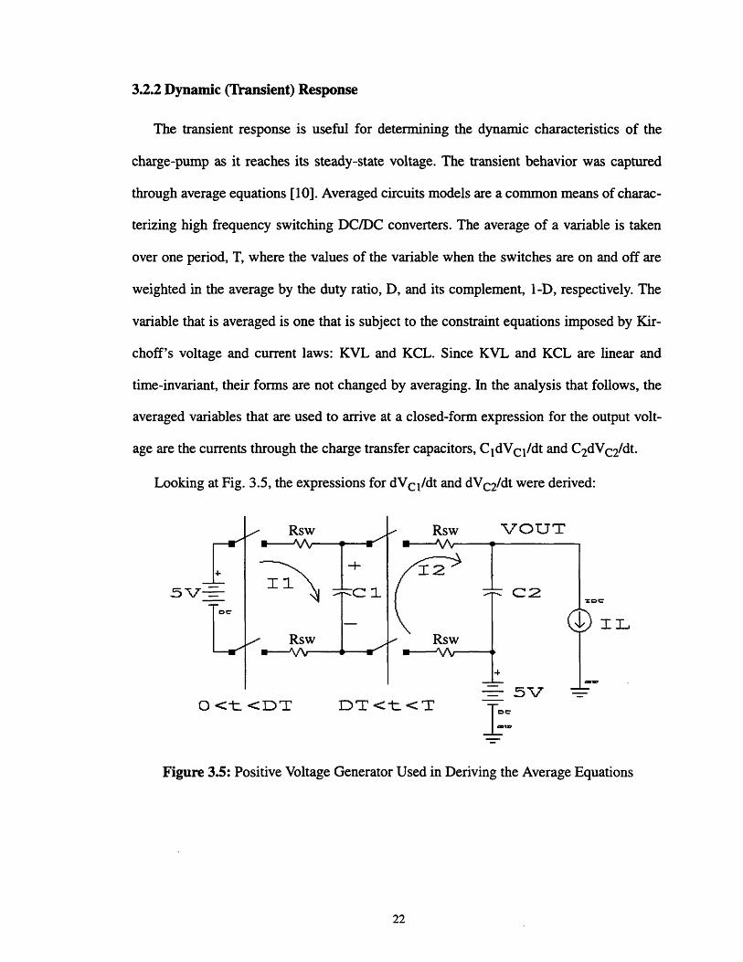
3.2.2 Dynamic (Transient) Response
The transient response is useful for determining the dynamic characteristics of the
charge-pump as it reaches its steady-state voltage. The transient behavior was captured
through average equations [10]. Averaged circuits models are a common means of charac-
terizing high frequency switching DC/DC converters. The average of a variable is taken
over one period, T, where the values of the variable when the switches are on and off are
weighted in the average by the duty ratio, D, and its complement, 1-D, respectively. The
variable that is averaged is one that is subject to the constraint equations imposed by Kir-
choff's voltage and current laws: KVL and KCL. Since KVL and KCL are linear and
time-invariant, their forms are not changed by averaging. In the analysis that follows, the
averaged variables that are used to arrive at a closed-form expression for the output volt-
age are the currents through the charge transfer capacitors, CldVcl/dt and C2dVc 2/dt.
Looking at Fig. 3.5, the expressions for dVcl/dt and dVc 2/dt were derived:
Rsw Rsw VOUT
125_ C1 C2
- ILRsw Rsw
4
-57 --O <-t <D T IDT <-t < T
Figure 3.5: Positive Voltage Generator Used in Deriving the Average Equations
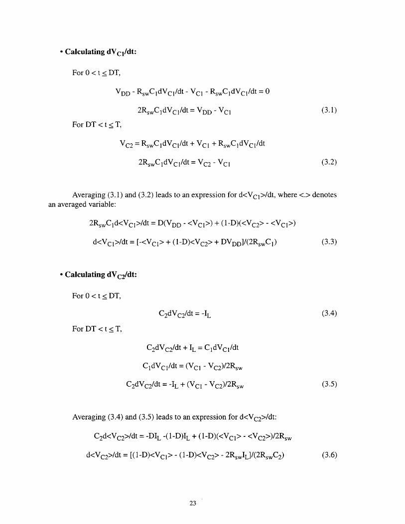
- Calculating dVc1/dt:
For 0 < t < DT,
VDD - RswCidVcl/dt - VC , - RswCidVcl/dt = 0
2RswC dVcl/dt = VDD - VCl (3.1)
For DT < t < T,
VC2 = RswCldVcl/dt + VCl + RswCldVcl/dt
2RswCldVc/dt = VC2 - VCI (3.2)
Averaging (3.1) and (3.2) leads to an expression for d<Vcl>/dt, where <.> denotesan averaged variable:
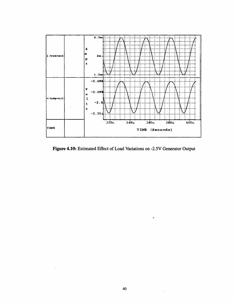
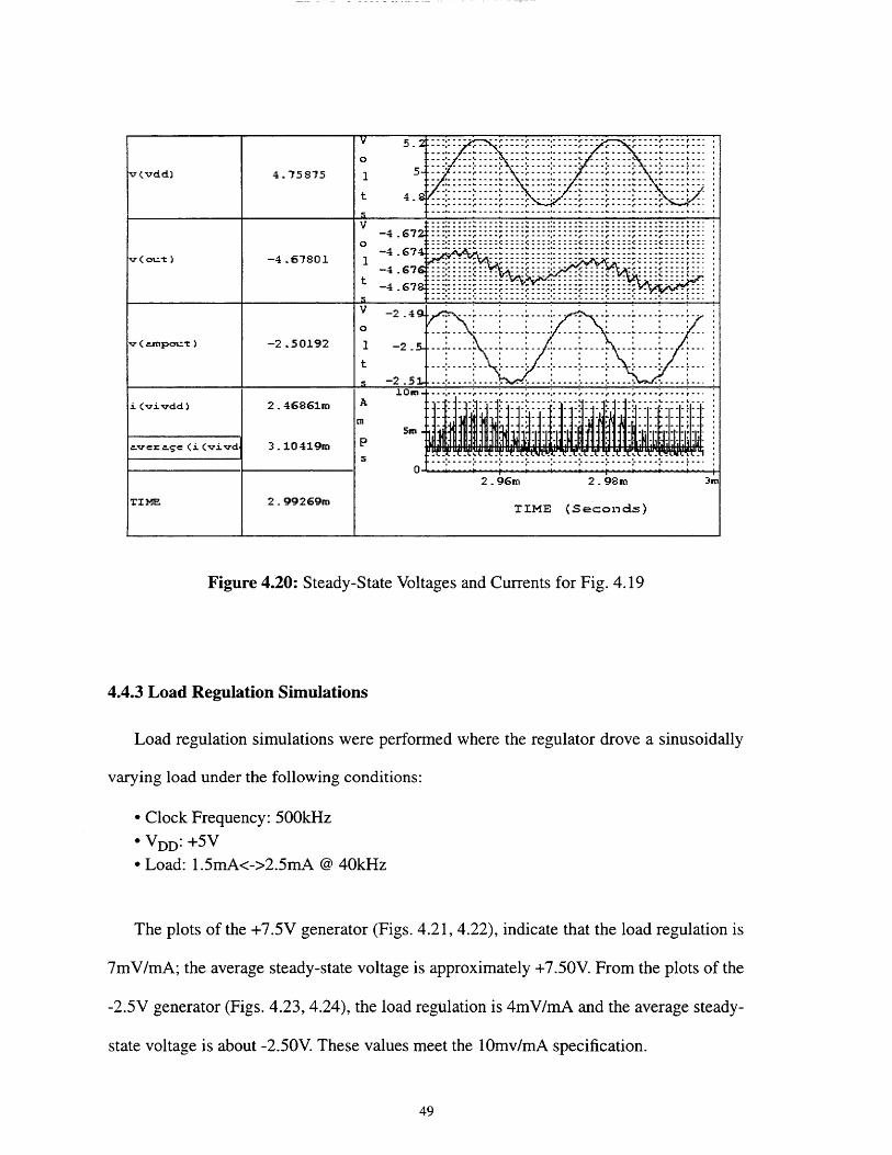
Figure 4.10: Estimated Effect of Load Variations on -2.5V Generator Output
40
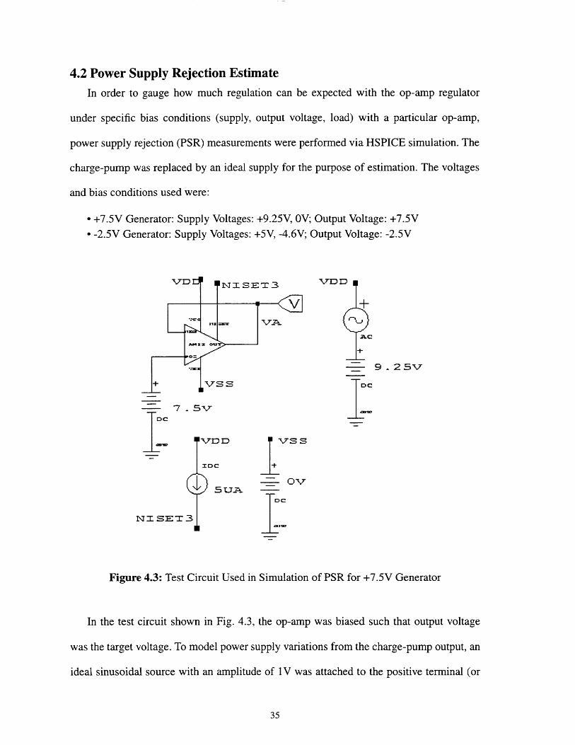
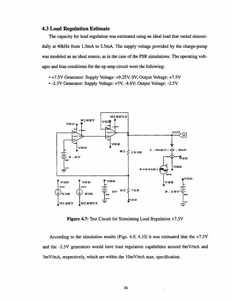
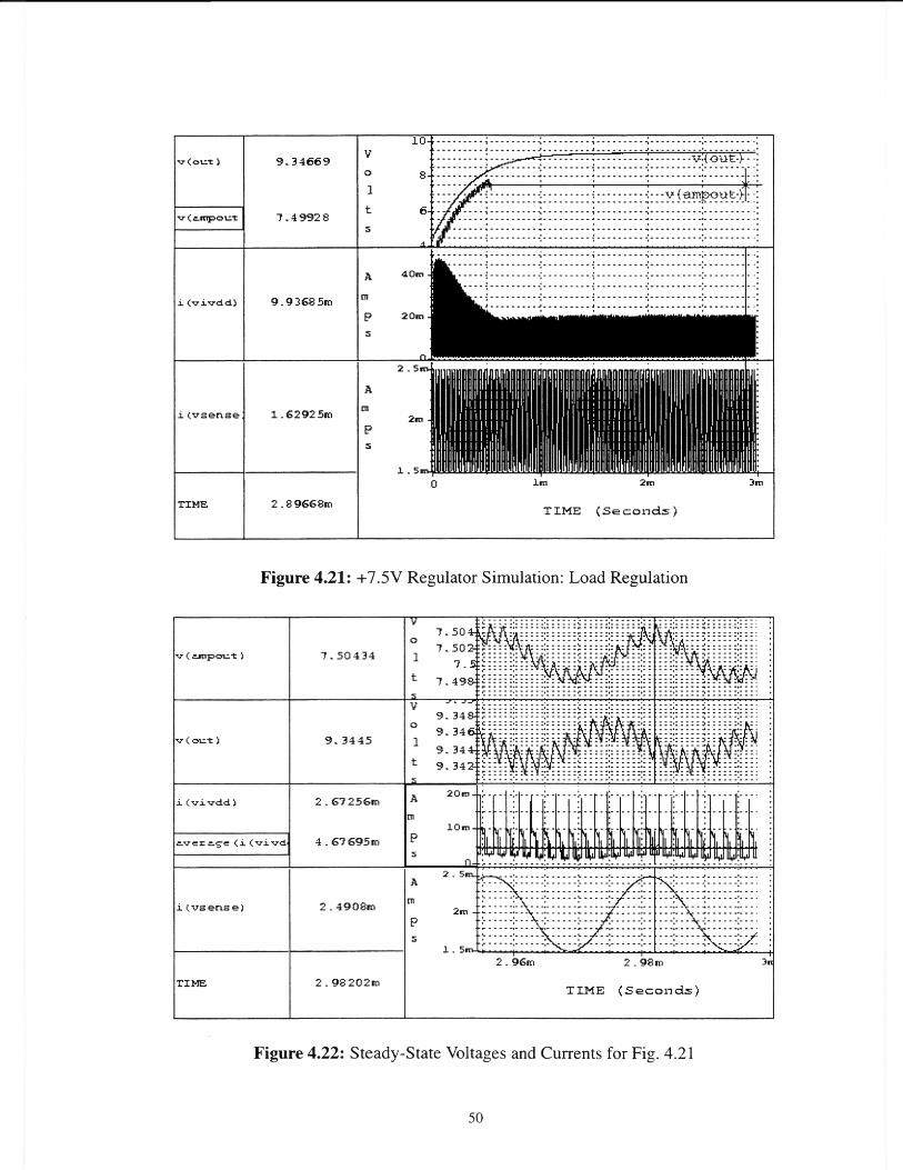
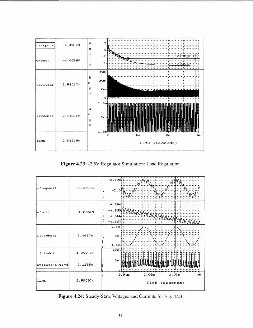
4.4 Simulation Results: Transient Measurements of Complete Converter
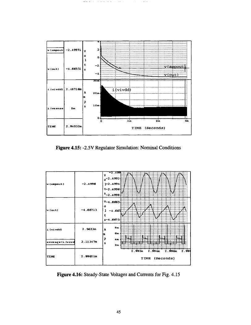
4.4.1 Simulations Under Nominal Conditions
Transient response measurements were performed with HSPICE for the complete con-
verter circuit which consists of the charge pump, the auxiliary circuits (break-before-make
circuit, level-shifter, startup circuit), and the op-amp regulator. The +7.5V and -2.5V con-
verters are featured in Fig. 4.11 and Fig. 4.12, respectively.
The nominal conditions under which the simulations took place are defined below:
* clock frequency: 500kHz
*VDD: +5V* Load: 2mA
From the plots of the transient repponse, one can extract the output voltage, the ripple,
the efficiency, power supply rejection and load regulation. The latter two were simulated
with a modified circuit with the appropriate sinusoidally varying circuit element (voltage
source or load).
The plots use the following voltage and current variables:
* v (ampout) : Output of the Op-Amp regulator (the target voltage)* v (out) : Output voltage of the unregulated charge-pump* v (vdd) : Supply voltage, VDD* i (vsense) : Load current* i (vivdd) : Current drawn from VDD* average (i (vivdd) ) : Average of the total current drawn from VDD (used in
efficiency calculation)
JLII
i. ,
. - "1....
Figure 4.11: Complete Converter/Regulator Circuit for +7.5V Generation
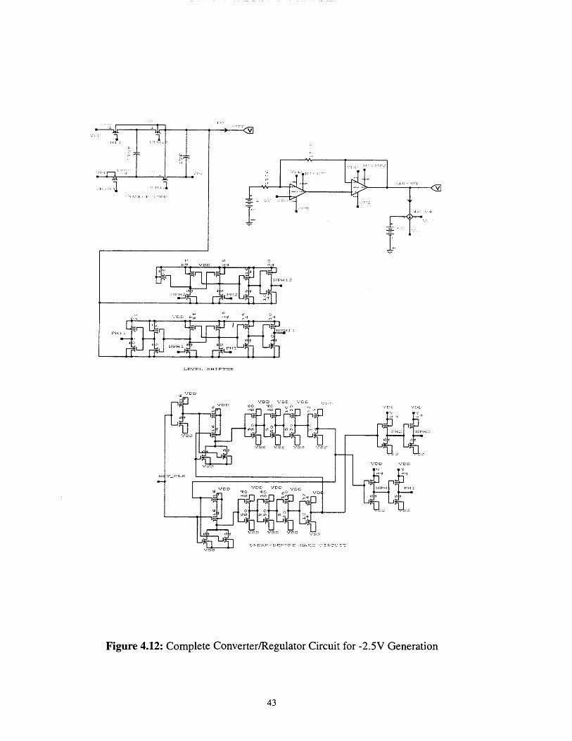
Figure 4.12: Complete Converter/Regulator Circuit for -2.5V Generation
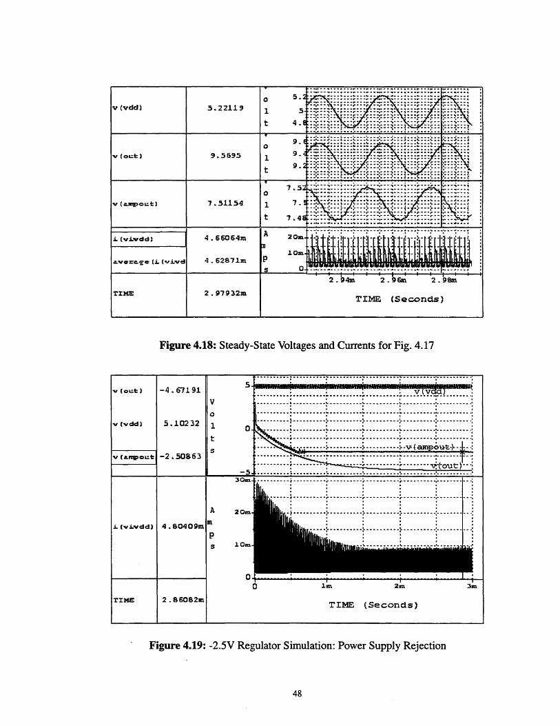
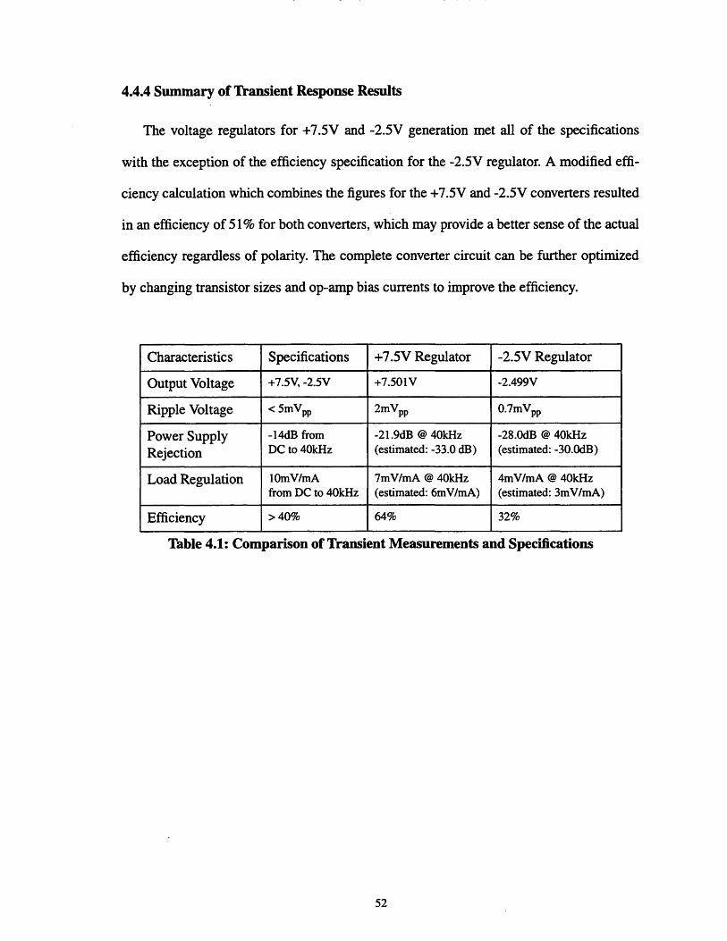
Power Supply -14dB from -21.9dB @ 40kHz -28.0dB @ 40kHz
Rejection DC to 40kHz (estimated: -33.0 dB) (estimated: -30.0dB)
Load Regulation 10mV/mA 7mV/mA @ 40kHz 4mV/mA @ 40kHzfrom DC to 40kHz (estimated: 6mV/mA) (estimated: 3mV/mA)
Efficiency > 40% 64% 32%
Table 4.1: Comparison of Transient Measurements and Specifications
Chapter 5
Other Output Regulation Schemes
5.1 Pulse Width ModulationA common way of controlling the output characteristics of a power converter is to use a
Pulse-Width Modulation (PWM) control scheme. A PWM controller consists of a saw-
tooth generator and a comparator comparing some form of the output voltage with the
sawtooth waveform to determine the appropriate pulse width of the switching clock. The
input to the comparator is often the output of an integrator which is useful for constructing
a system whose steady-state error must be zero.
Charge-Pump Output Lo ad
Transistor Switches
Error VoltageSawtooth Vref- Generator
Comparator CLKIntegrator
Figure 5.1: Block Diagram for PWM-Controlled Charge-Pump
For the DC/DC converter featured in this thesis, a PWM controller may be imple-
mented. However, this converter will not be as robust as the op-amp regulator under differ-
ent operating conditions (e.g. power supply and clock frequency variations). Early on, a
PWM controller was studied and the main problems that were encountered in its effective
implementation were the following: 1) dependence on the switching frequency; 2) awk-
ward algebraic tricks required to prevent op-amp saturation; and 3) poor power supply
rejection.
Dependence on Switching Frequency
The sawtooth waveform is dependent on the switching frequency. It is generated by
charging a capacitor where the time constant of charging is much longer than the switch-
ing period; the peak voltage, Vp, of the sawtooth waveform is Vp = IT/C. Therefore, a
change in the switching frequency will cause a change in the peak voltage of the sawtooth
waveform, which in turn changes the slope, and hence affects the pulse-width for a given
comparator trip voltage that is fed from the integrator. A circuit to minimize the depen-
dence on switching frequency was designed, but it was not robust over the 2Mhz+30% fre-
quency range. A circuit that can generate a sawtooth waveform whose peak voltage is a
constant with respect to frequency needs to be developed further if PWM is to be used in
this particular application.
Algebraic Tricks to Prevent Op-Amp Saturation
The supplies that were given were OV and +5V and the output voltages were -2.5V and
+7.5V; a +2.5V reference was provided. Since the numbers that were given were multiples
of 2.5, some minor algebraic manipulation were required to come up with the correct rela-
tions between 1) the output voltage, 2) the error voltage, and 3) the input to the comparator
such that the control loop could force the system to converge upon the correct output volt-
age without saturating the op-amps that are involved.
The issue of saturating op-amps comes up since the system is referenced to +2.5V and
the PWM control scheme would utilize a simple integrator, which inverts signals to a neg-
ative voltage. Given a 2.5V offset in the system, some amount of algebraic manipulation
was necessary to generate an appropriate error voltage from the output of the integrator to
be used as the comparator tripping voltage on the sawtooth waveform. Hence, it was very
convenient that the system reference was +2.5V and the output voltages were multiples of
it. If the desired output voltage was 8.25V, for example, there would have been difficulty
generating the correct error voltages and keeping the amplifiers, which are biased with
respect to 2.5V, from saturating to either supply voltage.
Poor Power Supply Rejection
The PWM controller had an integrator which integrated the error to zero at steady-
state. The integrator required another off-chip capacitor since its response had to be about
an order of magnitude slower than the 40kHz power supply variations. It was observed
that the PWM converter could not handle a 40kHz variation in the power supplies; after
20mS, there were no signs that the transient was dying out; the converter followed the
VDD variations regardless of the size of the capacitor on the integrator. Making the capac-
itor large had the effect of dampening the rise of the voltage to its specified output value
rather than filtering out the supply variations. When the capacitor was made too large, reg-
ulation did not occur at all.
In general, the PWM scheme may be more efficient than an op-amp regulator for
lighter loads since the width of the pulses are not set and can become arbitrarily small.
However, the PWM scheme investigated here for this set of specifications (frequency =
2MHz + 30%; 40kHz VDD variations) is not a robust design; a very specific operating
point (sawtooth trip-point at steady-state, a frequency-independent sawtooth peak), needs
to be established before it can be made to regulate. The PWM controller is not easily con-
figurable as a result. The difficulties that are outlined above render it an unattractive con-
trol scheme for the present application.
5.2 Pulse Frequency ModulationAnother way of regulating a DC/DC converter is by means of Pulse-Frequency Modula-
tion (PFM) where the clock is turned on and off. PFM systems can be implemented with a
comparator that compares the output voltage and then decides to either keep the clock on
or to turn it off. This control scheme takes up the least power since the controlling block is
a simple latch comparator [9] rather than two op-amps (Op-Amp controller) or a sawtooth
generator, integrator and comparator (PWM).
OutputCharge-PumpLoad
Transistor Switches ErrorVoltage VrefGenerator
Latch Comparator CLK
Figure 5.2: Block Diagram for PFM-Controlled Charge-Pump
For the purposes of the specific DC/DC converter featured in this thesis, a pulse-fre-
quency modulator was not an appropriate means of regulation for the following reason: A
PFM converter generates different frequencies from the frequency of the clock being
turned on and off by the latch comparator. This on/off frequency is a function of the load;
hence in a system where the load constantly changed, many different on/off frequencies
would be produced. For a system that is sensitive to the frequencies generated by its power
supply, such as a demodulator, a PFM converter is not advisable.
The benefits of a PFM converter is that it can be operated over a variety of frequency
ranges; the 2MHz+30% specification for the clock would not noticeably affect the perfor-
mance of the converter. Moreover, since the PFM converter is turned off and on, its effi-
ciency would be higher at light loads compared to other control schemes that were
discussed. Its static dissipation would be lower than the other regulation schemes as well.
58
Chapter 6
Conclusion
The performance of a DC/DC converter consisting of a charge-pump circuit and an op-
amp regulation scheme were analyzed. The specifications were comfortably met, with the
exception of optimum efficiency. Relying on the regulation properties of an op-amp
enabled the system to be decoupled; the charge-pump operated independently of the op-
amp. As a result, the target voltage is essentially generated independently of the charge-
pump's behavior. This simplifies designing the converter for an arbitrary voltage.
Other control schemes can be used, such as a linear feedback regulator, which controls
the gate biases of the switching transistors accordingly. In PWM, the pulse width is modu-
lated; in PFM, the pulse is either turned off or on. Perhaps the most noticeable difference
between the op-amp regulation schemes and those mentioned above is the decoupling of
the voltage generation function from its regulation mechanism. One of the possible rea-
sons why PWM was difficult to implement effectively was since the control loop directly
controlled the charge-pump, the poles of the system might have moved, leading to poor
power supply rejection. Because the steady-state and transient properties are a function of
the load, it may not be a robust design scheme to have a controller directly control the out-
put since the operating points will change with changing loads.
For a simple concept, the op-amp regulator, for this particular application, seems to be
the best control scheme given the set of specifications in Chapter 2.
60
References
[1] A. Stratakos, S. Sanders, and R. Brodersen, "A Low-Voltage CMOS DC-DCConverter for a Portable Battery-Operated System," Proc. IEEE Power ElectronicsConf., pp. 619-626, 1994.
[2] C. Wang and J. Wu, "Efficiency Improvement in Charge Pump Circuits," IEEEJournal of Solid-State Circuits, Vol. 32, No. 6, pp. 852-860, June 1997.
[3] C. Calligaro, R. Gastaldi, P. Malcovati, and G. Torelli, "Positive and NegativeCMOS Voltage Multiplier for 5V-Only Flash Memories," Proc. IEEE 38th MidwestSymposium on Circuits and Systems, Vol. 1, pp. 294-297, 1995.
[4] K. Sawada, Y. Sugawara, and S. Masui, "An On-Chip High-Voltage GeneratorCircuit for EEPROMS with a Power Supply Voltage below 2V," Symposium on VLSICircuits Digest of Technical Papers, pp. 75-76, 1995.
[5] M. Shoji, CMOS Digital Circuit Technology, pp. 306-307, Prentice-Hall, EnglewoodCliffs, NJ, 1988.
[6] N. Weste and K. Eshragian, Principles of CMOS VLSIDesign, pp. 319-320, Addison-Wesley, New York, Second Edition, 1993.
[7] P. Favrat, P. Deval, and M. Declercq, "A New High Efficiency CMOS VoltageDoubler," Proc. IEEE Custom Integrated Circuits Conf., pp. 259-262, 1997.
[8] L. Casey, J. Ofori-Tenkorang, and M. Schlecht, "CMOS Drive and Control Circuitryfor 1-10 MHz Power Conversion," IEEE Transactions on Power Electronics, Vol. 6,No. 4, pp. 749-758, Oct., 1991.
[9] J. Ho and H. Luong, "A 3V, 1.47mW, 120MHz Comparator for Use in a PipelineADC," Proc. IEEE Asia Pacific Conf. on Circuits and Systems, pp. 413-416, 1996.
[10] J. Kassakian, M. Schlecht, and G. Verghese, Principles of Power Electronics,Addison-Wesley, Reading, Massachusetts, 1991.