A transparent electrode based on a metalnanotrough networkHui Wu1,2†, Desheng Kong1†, Zhichao Ruan3, Po-Chun Hsu1, Shuang Wang3, Zongfu Yu3,
Thomas J. Carney1, Liangbing Hu1, Shanhui Fan3 and Yi Cui1,4*
Transparent conducting electrodes are essential componentsfor numerous flexible optoelectronic devices, including touchscreens and interactive electronics1–4. Thin films of indium tinoxide—the prototypical transparent electrode material—demonstrate excellent electronic performances, but film brittle-ness, low infrared transmittance and low abundance limit suit-ability for certain industrial applications1,4,5. Alternatives toindium tin oxide have recently been reported and include con-ducting polymers6, carbon nanotubes7–9 and graphene10–12.However, although flexibility is greatly improved, the optoelec-tronic performance of these carbon-based materials is limitedby low conductivity8,13. Other examples include metal nano-wire-based electrodes14–22, which can achieve sheet resistancesof less than 10VA21 at 90% transmission because of the highconductivity of the metals. To achieve these performances,however, metal nanowires must be defect-free, have conduc-tivities close to their values in bulk, be as long as possible tominimize the number of wire-to-wire junctions, and exhibitsmall junction resistance. Here, we present a facile fabricationprocess that allows us to satisfy all these requirements andfabricate a new kind of transparent conducting electrode thatexhibits both superior optoelectronic performances (sheetresistance of ∼2VA21 at 90% transmission) and remarkablemechanical flexibility under both stretching and bendingstresses. The electrode is composed of a free-standing metallicnanotrough network and is produced with a process involvingelectrospinning and metal deposition. We demonstrate thepractical suitability of our transparent conducting electrodeby fabricating a flexible touch-screen device and a transparentconducting tape.
The process for fabricating our nanotrough network is based ontemplating ultralong polymer nanofibres (Fig. 1a). In the first step,continuous polymer nanofibre webs are prepared by means of elec-trospinning23, a low-cost and scalable approach for forming longpolymer fibres assembled in random networks or oriented arrayscontrolled by the geometry of the fibre collector (SupplementaryFig. S1). Note that the electrospun fibres can bridge an extremelylong distance (across a gap of more 6 inches, as shown inSupplementary Fig. S2). In the second step, the free-standingpolymer nanofibre networks are coated with a thin layer of materialusing standard thin-film deposition techniques, such as thermalevaporation, electron-beam evaporation or magnetron sputtering24,allowing a rich variety of functional materials to be prepared whileretaining a bulk-like electrical conductivity. Owing to the direction-ality of these deposition processes24, the polymer fibres are preferen-tially coated on one side, thus forming nanotroughs with a concave
cross-section (Fig. 1c, Supplementary Fig. S3). The coated polymerfibres are mechanically flexible and robust, and can be transferredeasily onto various substrates to interface with macroscopic-scalesystems. In the third step, after transferring the fibre, the polymertemplates are removed by submerging the entire electrode inwater or other organic solvents. Using this method, we have fabri-cated continuous nanotrough networks from a wide variety of func-tional materials, including silicon, indium tin oxide (ITO)(Supplementary Fig. S4) and metals such as gold (Fig. 1b), silver,copper, platinum, aluminium, chromium, nickel and their alloys(Supplementary Fig. S5).
The microstructure of the nanotroughs was characterized byscanning electron microscopy (SEM). Figure 1b shows a typicalexample of a nanotrough network, in this case a uniformnetwork of intertwined gold nanotroughs with widths of�400 nm and lengths greater than 1 mm. It is important to notethat individual nanotroughs are naturally interconnected at theirjunctions during metal deposition (Fig. 1b). A side-view SEMimage of the synthesized nanotroughs (Fig. 1c) confirms thatpolymer fibre templates have been fully removed, leaving solidribbons with concave cross-sections. The thickness of each troughis �80 nm, and can be varied easily by changing the metal depo-sition time. The average width of each trough is 406 nm(Supplementary Fig. S6) and can be adjusted by controlling thediameter of the polymer fibre template by means of electrospinning.Figure 1d shows examples of gold nanotroughs successfullyattached to different surfaces, including a glass slide, polyethyleneterephthalate (PET) plastic, paper, a textile and a curved glassflask, all without any surface treatment, and making all the surfaceshighly conducting (Fig. 1d, Supplementary Fig. S9). The nano-troughs are firmly attached to the substrates (SupplementaryFig. S7) and cannot be peeled off with scotch tape(Supplementary Movie S1).
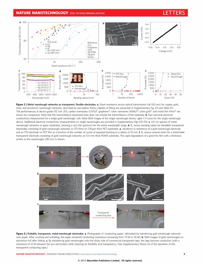
Metal films with thicknesses greater than 80 nm usually have lowtransmittance25, but our metal nanotroughs are highly transparent(Supplementary Fig. S10). Figure 2a plots the transmittance of themetal nanotrough electrodes on glass substrates with various sheetresistances Rs. The Rs values of copper, gold and silver nanotroughswith �90% optical transmittance are �2, 8 and 10VA21, respect-ively. Copper nanotrough networks demonstrated the best perform-ance—2VA21 at T¼ 90%, 10VA21 at T¼ 95% and 17VA21 atT¼ 97%—a performance that is comparable to state-of-the-artdevice-grade ITO20 and superior to other transparent conductingelectrodes such as those based on graphene, carbon-nanotubefilms, solution-processed silver or copper nanowires, metal grids,thin metal films and conducting polymers (Fig. 2a)7,8,12,14,16,17,20,25–27.
1Department of Materials Science and Engineering, Stanford University, California 94305, USA, 2State Key Lab of New Ceramics and Fine Processing,School of Materials Science and Engineering, Tsinghua University, Beijing 100084, China, 3Department of Electrical Engineering, Stanford University,California 94305, USA, 4Stanford Institute for Materials and Energy Sciences, SLAC National Accelerator Laboratory, 2575 Sand Hill Road, Menlo Park,California 94025, USA, †These authors contributed equally to this work. *e-mail: [email protected]
LETTERSPUBLISHED ONLINE: 19 MAY 2013 | DOI: 10.1038/NNANO.2013.84
The remarkable performance of nanotrough electrodes can beattributed to several main factors. First, the metal nanotroughs areproduced using a standard thin-film deposition process, whichyields high-quality metals. For example, a single gold nanotroughhas an electric conductivity of �2.2 × 10⁵ S cm21 (measured by afour-point probe), which is comparable to its polycrystalline bulkvalue (4.1 × 10⁵ S cm21) (Fig. 2b, Supplementary Figs S12 and S13).It is important to note that nanostructured metals usually havesignificantly lower conductivity compared to their bulk counterpart,possibly due to impurities incorporated during synthesis, reducedcrystal quality, contaminants or surfactants on the surface, and elec-tron scattering. For example, the conductivity of a single-crystallinesilver nanowire is approximately ten times lower than that of thebulk crystal28. In contrast, our nanotroughs exhibit an electrical con-ductivity that is approximately half that of the bulk, possibly a resultof the evaporation process, which produces clean and high-quality metals.
Second, the nanotroughs form a highly uniform, interconnectednetwork. The properties of these nanotrough electrodes are welldescribed by percolation theory (Supplementary Fig. S11)29.These nanotrough networks are required to have exceptionalpercolation parameters to achieve high-performance transparentconducting electrodes (Supplementary Table S1). It has beenshown that percolation parameters largely depend on the
uniformity of the network22. The improvement observed herecan therefore be ascribed to the spatially uniform network that isa consequence of the evenly distributed polymer nanofibre tem-plate achieved by the electrospinning process. The interconnectedstructure of the nanotrough network (Fig. 1b) also avoids the cre-ation of a large junction resistance, a common bottleneck in metalnanowire networks15.
Third, the concave shape of the nanotroughs reducesthe electromagnetic cross-section, which allows more visiblelight to pass through in comparison to flat nanostripes(Supplementary Fig. S15).
The metal nanotrough networks demonstrate flat transmittancespectra from 300 nm to 2,000 nm (Fig. 2c, SupplementaryFig. S16). Wideband flat spectra are highly desirable for manyoptoelectronic devices as they simplify the optics by removingadditional chromatic correction components, enable applicationsin near-infrared sensors and detectors, and may enhance solar cellefficiency by using the near-infrared solar spectrum (where conven-tional ITO conductors become almost opaque3).
Chemical stability is another important concern for transparentconducting electrodes. Supplementary Fig. S17 shows the change inresistance in various metal nanotrough networks upon exposure tohigh temperatures and humidity. The chemical stability can beimproved significantly with surface passivation, as demonstrated
b
d
200 nm
c
1 mm
200 nm
V
a
Electrospinning
Fibre web Nanotrough web
Laminated on substratesDissolving fibre template
Figure 1 | Fabrication and transfer process for nanotroughs. a, Schematic of the polymer-nanofibre templating process for fabricating nanotroughs. Polymer
nanofibre templates were first made by electrospinning, then coated with selected materials using standard thin-film deposition techniques. The coated fibres
were transferred onto a solid substrate. The substrate was subsequently dipped in water or an organic solvent to dissolve away the polymer-fibre template.
b, Top-view SEM images of gold nanotrough networks (left) and a junction between two nanotroughs (right). c, SEM image of the cross-section of a single
gold nanotrough, revealing its concave shape. d, Gold nanotrough networks can be transferred easily onto various substrates, including a glass slide, PET
plastic, paper, textile and a curved glass flask (left to right).
Figure 2 | Metal nanotrough networks as transparent, flexible electrodes. a, Sheet resistance versus optical transmission (at 550 nm) for copper, gold,
silver and aluminium nanotrough networks, described by percolation theory (details of fitting are presented in Supplementary Fig. S11 and Table S1).
The performances of device-grade ITO (ref. 20), carbon nanotubes (CNTs)8, graphene12, silver nanowires (NWs)20, silver grid27 and nickel thin films25 are
shown for comparison. Note that the transmittance mentioned here does not include the transmittance of the substrate. b, Four-terminal electrical
conductivity measurement for a single gold nanotrough. Left: tilted SEM images of the single nanotrough device; right: I–V curve for the single nanotrough
device. Additional electrical conductivity measurements on single nanotroughs are provided in Supplementary Figs S12–S14. c, UV–vis spectra of metal
nanotrough networks on glass substrates, showing a very flat spectrum for the entire wavelength range. d, Rs versus bending radius for bendable transparent
electrodes consisting of gold nanotrough networks or ITO films on 178-mm-thick PET substrates. e, Variations in resistance of a gold nanotrough electrode
and an ITO electrode on PET film as a function of the number of cycles of repeated bending to a radius of 10 mm. f, Rs versus uniaxial strain for a stretchable
transparent electrode consisting of gold nanotrough networks on 0.5-mm-thick PDMS substrate. The rapid degradation of a gold thin film with a thickness
similar to the nanotroughs (80 nm) is shown.
a
b
c
Transparent conducting tape
1 μm 1 μm20 μm
Figure 3 | Foldable, transparent, metal-nanotrough electrodes. a, Photographs of ‘conducting paper’, fabricated by transferring gold nanotrough networks
onto paper. After crushing and unfolding, the paper remained conducting (resistance increasing from 73 V to 131 V). b, SEM images of gold nanotroughs on
aluminium foil after folding. c, By transferring gold nanotroughs onto the sticky side of commercial transparent tape, the tape became conductive (with a
resistance of 22 V between the two electrodes) while retaining its flexibility and transparency. (See Supplementary Movie S2 of the operation of this
in our previous study on copper nanofibres30. Passivation of thenanotroughs is beyond the scope of the current study and will bea valid future research topic.
Our metal nanotrough networks are bendable, stretchable andfoldable. To examine their mechanical durability, we transferredthe networks onto a 178-mm-thick PET substrate and either bentthe film down to a radius of 2 mm (Fig. 2d) or repetitively bentthe film to 20 mm, 2,000 times (Fig. 2e). On examining the trans-parent electrode after both bending regimes, we could find noobvious degradation in electrical conductivity. In contrast, severedegradation in conductivity is observed in ITO films after bendingto ,50 mm, or bending to 20 mm more than 20 times (Fig. 2d,e).The stretchability of the transparent electrodes was examined bytransferring the nanotrough networks onto a substrate of poly(di-methylsiloxane) (PDMS) without surface activation. The sheetresistance increased by �40% after being stretched uniaxiallyto 50% strain, which is comparable to the performance of
carbon-nanotube-based transparent elastic conductors2 and ingreat contrast to the dramatic increase in resistance observed inmetal films of similar thickness (Fig. 2f).
We also transferred nanotrough networks onto paper to test theirmechanical properties under extreme conditions. After crushingand then unfolding the electrode on paper, the electrode remainedconductive, with only a limited change in the resistance (Fig. 3a,Supplementary Fig. S18). The mechanistic explanation is that thenanotroughs remain continuous during folding, undergoing nano-scale deformation to relax the applied stress (Fig. 3b). Moreover,SEM images show that a free-standing metal nanotrough networkcan be folded without fracturing (Supplementary Fig. S19). Thesedurable nanotrough networks can also be transferred onto commer-cial cellulose tape to produce transparent conducting tape (Fig. 3c,Supplementary Movie S2). This transparent conducting tape canstick easily onto a material surface, making the surface conductivewithout any surface treatment. This new technique may enableeasy integration of optoelectronic devices and possibly expand theareas of application of transparent conducting electrodes.
Because of the many advantages of metal nanotrough electrodes,including facile fabrication, ease of transfer, high transparency andsuperior flexibility, these electrodes are readily applicable in practi-cal optoelectronic devices. Indeed, we have demonstrated a high-performance nanotrough electrode incorporated into a resistivetouch-screen device (Supplementary Fig. S20). The operation ofthis device is demonstrated in Supplementary Movie S3.
Finally, the unique concave shape and nanoscale dimensions ofour continuous metal nanotroughs also lead to interestingoptical properties. To understand the interaction between an inci-dent light field and the nanotrough, we numerically solvedMaxwell’s equations and obtained the near-field distribution oflight intensity around the nanotrough. Our simulation predicts alocalized ‘light-focusing’ phenomenon associated with this struc-ture, which effectively concentrates light in the vicinity of themetal nanotroughs (Fig. 4). For transverse magnetic (TM) polariz-ation (Fig. 4a), the field intensity is enhanced almost seven timesaround the inner boundary of the ribbon due to well-knownsurface plasmonic effects. Interestingly, for transverse electrical(TE) polarization, even without the surface plasmonic effect thenanotroughs still provide a significant light concentration effect,with the field intensity enhanced by a factor of about 6.5 at thecentre (Fig. 4b). This is due to the unique cross-section of theribbon, which mimics the action of a macroscopic trough reflectorto maximize the field intensity at the centre. The novel localizedlight (or energy) concentration effects are expected to be usefulfor many optoelectronic applications, including solar cells, solarfuels, photo-assisted localized chemical reactions andoptical sensors.
In summary, we have shown that metal nanotrough transparentconducting electrodes exhibit both excellent optoelectronic per-formance (to compete with device-grade ITO) and remarkablemechanical properties (to tolerate large bending and stretchingstresses). Their synthesis is facile and amenable to scale up basedon standard electrospinning and metal deposition techniques.Such metal nanotrough electrodes could replace ITO, which iswidely used in solar cells, touch sensors and flat panel displays,and could find use in emerging application areas such as flexibleelectronics and skin-like sensors2.
MethodsNanotrough fabrication. The polymer nanofibre template was produced usingelectrospinning, a well-known technique for making continuous ultralongnanofibres at low cost and in large quantity. Water-soluble polymers includingpolyvinyl alcohol (PVA, Sigma-Aldrich) and polyvinylpyrrolidone (PVP, Sigma-Aldrich) were selected as the raw materials to produce naturally degradablepolymer templates. The precursor solution was made by adding polymer powder(10 wt% PVA or 14 wt% PVP) to deionized water then stirring at 80 8C for 10 h.
a
0.5
TM
TE
0.4
0.3
0.2
0.1
0.0
−0.5
−0.4
−0.3
−0.2
−0.1
y (μ
m)
0.5
0.4
0.3
0.2
0.1
0.0
−0.5
−0.4
−0.3
−0.2
−0.1
y (μ
m)
0.50.40.30.20.10.0−0.5−0.4−0.3 −0.2 −0.1x (μm)
0.50.40.30.20.10.0−0.5−0.4−0.3 −0.2 −0.1x (μm)
k
k
8
6
4
0
2
b
8
6
4
0
2
Figure 4 | Optical simulation of a single metal nanotrough. a,b, Intensity
distribution of TM (a) and TE (b) fields in the vicinity of a gold nanotrough,
at a wavelength of 540 nm, where a plane wave with unitary amplitude is
incident on the nanotrough from bottom to top. The diameter and thickness
of the nanotrough are 460 nm and 80 nm, respectively. Simulation is
performed by numerically solving Maxwell’s equations using a finite-element
A voltage of 15 kV was applied to the solution using a high-voltage source (GammaHigh Voltage Research, model ES30P-5W) to spin fibres out of a needle. Thefree-standing fibres gradually formed a network, which was collected in a copperframe. The density of nanofibres could be controlled by altering the electrospinningtime. Metal nanotroughs were prepared at a base pressure of 1 × 1026 torr bythermal evaporation (Mbraun glovebox integrated evaporator system) ofchromium, gold, copper, silver and aluminium, and electron-beam evaporation(Temescal electron-beam evaporator) of platinum and nickel. For the metalnanotrough networks used as transparent electrodes, a constant thickness of 100 nmwas deposited for all metals, unless otherwise specified. The sample temperaturewas kept below 60 8C during evaporation. Silicon and ITO nanotroughs weregenerated based on a.c. magnetosputtering (AJA ORION sputtering system) with alow power of 125 W and a pressure of 5 mtorr. Note that the quality of thenanotroughs was affected by the choice of polymer templates (SupplementaryFig. S8). Accordingly, PVP nanofibre templates were selected for the nanotroughsof gold, platinum, silicon and ITO, whereas PVA nanofibre templates were usedfor copper, silver and aluminium.
Optical and electrical characterization. The sheet resistances of the films weremeasured using a digital multimeter (Keithley 2100) with a four-point probeconfiguration to eliminate contact resistance. The conductivity of thenanotroughs was determined using a single nanotrough device. The conductivenetworks were sonicated in ethanol to form a suspension containing individualnanotroughs. The nanotroughs were dropcast onto an oxidized silicon substrate andpatterned into devices by means of standard electron-beam photolithographyand thermal evaporation of chromium/gold (10 nm/190 nm) contacts. Thenanotrough device was then measured using an Agilent B1500A semiconductordevice analyser. The transmittance measurement used a quartz tungsten halogenlamp as the light source, coupled with a monochromator (Newport 70528) to controlthe wavelength. An iris and a convex lens were used to focus the beam size to�1 mm × 2 mm, and a beamsplitter split the light beam into an integrating sphere(Newport, for transmittance measurement) and a photodiode (Newport, 818-UV-L).The photodiode was connected to an electrometer (Keithley 6517A) for lightintensity calibration. The samples were placed in front of the integrating sphere, sospecular light, diffuse light and haze were all included. An identical glass slidewas used for reference. A source-measure unit (Keithley 236) was used to measurethe photocurrent from the integrating sphere, and the transmittance was thuscalculated based on the reference plain glass slide. Accordingly, the measuredtransmittance did not include the transmittance of the glass substrates.
Touch-screen device fabrication. The four-wire analogue-resistive touch-screendevice was rebuilt from a commercial product from TVI Electronics. The 2.8-inchdevice consisted of an ITO electrode on a PET film and a piece of ITO glass,which were separated by square arrays of polymer spacer dots. In the rebuiltdevice, the ITO/PET film was replaced with a gold nanotrough network on 178-mm-thick PET. To prepare the gold nanotrough transparent conducting electrodecomponent, the gold nanotrough network was transferred onto the PET substrate,and then patterned with a 400-nm-thick copper circuit with the aid of a plastichard mask. The copper circuit allowed the gold nanotrough electrode to connectwith a commercial controller (also from TVI Electronics), which interfaced withthe computer. The sandwich-structure device was finally sealed with double-sided tape. Testing software was also provided by the vendor.
Received 26 July 2012; accepted 11 April 2013;published online 19 May 2013
References1. Fortunato, E., Ginley, D., Hosono, H. & Paine, D. C. Transparent conducting
oxides for photovoltaics. Mater. Res. Soc. Bull. 32, 242–247 (2007).2. Lipomi, D. J. et al. Skin-like pressure and strain sensors based on
transparent elastic films of carbon nanotubes. Nature Nanotech. 6,788–792 (2011).
3. Peng, H. L. et al. Topological insulator nanostructures for near-infraredtransparent flexible electrodes. Nature Chem. 4, 281–286 (2012).
4. Kumar, A. & Zhou, C. W. The race to replace tin-doped indium oxide:which material will win? ACS Nano 4, 11–14 (2010).
5. Tahar, R. B. H., Ban, T., Ohya, Y. & Takahashi, Y. Tin doped indium oxidethin films: electrical properties. J. Appl. Phys. 83, 2631–2645 (1998).
6. Kirchmeyer, S. & Reuter, K. Scientific importance, properties and growingapplications of poly(3,4-ethylenedioxythiophene). J. Mater. Chem. 15,2077–2088 (2005).
7. Zhang, M. et al. Strong, transparent, multifunctional, carbon nanotubesheets. Science 309, 1215–1219 (2005).
8. Hecht, D. S., Hu, L. B. & Irvin, G. Emerging transparent electrodes based onthin films of carbon nanotubes, graphene, and metallic nanostructures. Adv.Mater. 23, 1482–1513 (2011).
9. Niu, C. M. Carbon nanotube transparent conducting films. Mater. Res. Soc. Bull.36, 766–773 (2011).
10. Kim, K. S. et al. Large-scale pattern growth of graphene films for stretchabletransparent electrodes. Nature 457, 706–710 (2009).
11. Bonaccorso, F., Sun, Z., Hasan, T. & Ferrari, A. C. Graphene photonics andoptoelectronics. Nature Photon. 4, 611–622 (2010).
12. Bae, S. et al. Roll-to-roll production of 30-inch graphene films fortransparent electrodes. Nature Nanotech. 5, 574–578 (2010).
13. Hecht, D. S. & Kaner, R. B. Solution-processed transparent electrodes. Mater.Res. Soc. Bull. 36, 749–755 (2011).
14. De, S. et al. Silver nanowire networks as flexible, transparent, conductingfilms: extremely high DC to optical conductivity ratios. ACS Nano 3,1767–1774 (2009).
15. Garnett, E. C. et al. Self-limited plasmonic welding of silver nanowire junctions.Nature Mater. 11, 241–249 (2012).
16. Hu, L. B., Wu, H. & Cui, Y. Metal nanogrids, nanowires, and nanofibres fortransparent electrodes. Mater. Res. Soc. Bull. 36, 760–765 (2011).
17. Wu, H. et al. Electrospun metal nanofibre webs as high-performancetransparent electrode. Nano Lett. 10, 4242–4248 (2010).
18. Kang, M. G., Kim, M. S., Kim, J. S. & Guo, L. J. Organic solar cells usingnanoimprinted transparent metal electrodes. Adv. Mater. 20, 4408–4413 (2008).
19. Van de Groep, J. V., Spinelli, P. & Polman, A. Transparent conductingsilver nanowire networks. Nano Lett. 12, 3138–3144 (2012).
20. Leem, D. S. et al. Efficient organic solar cells with solution-processed silvernanowire electrodes. Adv. Mater. 23, 4371–4375 (2011).
21. Lyons, P. E. et al. High-performance transparent conductors from networksof gold nanowires. J. Phys. Chem. Lett. 2, 3058–3062 (2011).
22. Scardaci, V., Coull, R., Lyons, P. E. Rickard, D. & Coleman, J. N. Spray depositionof highly transparent, low-resistance networks of silver nanowires over largeareas. Small 7, 2621–2628 (2011).
23. Li, D. & Xia, Y. N. Electrospinning of nanofibres: Reinventing the wheel?Adv. Mater. 16, 1151–1170 (2004).
24. Kelly, P. J. & Arnell, R. D. Magnetron sputtering: a review of recentdevelopments and applications. Vacuum 56, 159–172 (2000).
25. Ghosh, D. S. Martinez, L., Giurgola, S., Vergani, P. & Pruneri, V. Widelytransparent electrodes based on ultrathin metals. Opt. Lett. 34, 325–327 (2009).
26. Lipomi, D. J. et al. Electronic properties of transparent conductive films ofPEDOT:PSS on stretchable substrates. Chem. Mater. 24, 373–382 (2012).
27. Lee, J-Y., Connor, S. T., Cui, Y. & Peumans, P. Solution-processed metalnanowire mesh transparent electrodes. Nano Lett. 8, 689–692 (2008).
28. Sun, Y. G., Gates, B., Mayers, B. & Xia, Y. N. Crystalline silver nanowires bysoft solution processing. Nano Lett. 2, 165–168 (2002).
29. De, S. & Coleman, J. N. The effects of percolation in nanostructuredtransparent conductors. Mater. Res. Soc. Bull. 36, 774–781 (2011).
30. Hsu, P. C. et al. Passivation coating on electrospun copper nanofibres forstable transparent electrodes. ACS Nano 6, 5150–5156 (2012).
AcknowledgementsThis material is based upon work supported as part of the Center on Nanostructuring forEfficient Energy Conversion (CNEEC) at Stanford University, an Energy Frontier ResearchCenter funded by the US Department of Energy, Office of Science, Office of Basic EnergySciences under Award Number DE-SC0001060, and the National Basic Research of China(grant no. 2013CB632702).
Author contributionsH.W. and Y.C. conceived the idea. H.W. and D.K. performed materials fabrication andtests. Z.C.R., Z.F.Y. and S.H.F. designed and carried out the optical simulations. H.W. andD.K. co-wrote the paper. All authors discussed the results and commented onthe manuscript.
Additional informationSupplementary information is available in the online version of the paper. Reprints andpermissions information is available online at www.nature.com/reprints. Correspondence andrequests for materials should be addressed to Y.C.
Competing financial interestsThe authors declare no competing financial interests.