Page 1
A universal low-noise analog receiver baseband in 65-nm CMOS
Ahmet Tekin • Hassan Elwan • Kenneth Pedrotti
Received: 14 October 2009 / Revised: 16 March 2010 / Accepted: 14 May 2010 / Published online: 30 May 2010
� The Author(s) 2010. This article is published with open access at Springerlink.com
Abstract In this paper, a novel universal receiver base-
band approach is introduced. The chain includes a post-
mixer noise shaping blocker pre-filter, a programmable-gain
post mixer amplifier (PMA) with blocker suppression, a
differential ramp-based novel linear-in-dB variable gain
amplifier and a Sallen–Key output buffer. The 1.2-V chain
is implemented in a 65-nm CMOS process, occupying a die
area of 0.45 mm2. The total power consumption of the
baseband chain is 11.5 mW. The device can be tuned across
a bandwidth of 700-KHz to 5.2-MHz with 20 kHz resolu-
tion and is tested for two distinct mobile-TV applications;
integrated services digital broadcasting-terrestrial ISDB-T
(3-segment fc = 700 kHz) and digital video broadcasting-
terrestrial/handheld (DVB-T/H fc = 3.8 MHz). The mea-
sured IIP3 of the whole chain for the adjacent blocker
channel is 24.2 and 24 dBm for the ISDB-T and DVB-T/H
modes, respectively. The measured input-referred noise
density is 10.5 nV/sqrtHz in DVB-T/H mode and 14.5 nV/
sqrtHz in ISDB-T mode.
Keywords Low-noise receiver � Noise-shaping
blocker filtering � Frequency dependent negative
resistance (FDNR) � Post mixer amplifier (PMA) �Variable gain amplifier (VGA)
1 Introduction
Many new wireless standards have emerged in recent years
as a result of strong consumer demand in wireless appli-
cations. The abundance of these wireless applications,
increasing demand and crowding of the spectrum pose
challenges for designers. These emerging wireless stan-
dards have to be backward compatible with the existing
standards. Hence, very strong interferers can coexist in the
nearby channels whereas the desired signal in the channel
of interest might be very weak. This is particularly the case
for mobile-TV applications, where 46-dB stronger analog
interferers can exist in the close vicinity of desired channel
[1]. As a result, the classical noise-linearity-power-area
tradeoff becomes an even more pronounced challenge in
wireless receiver design. Battery life concerns require low
power compact solutions for portable devices must allow a
low-power operation. To reduce system size designs should
be reconfigurable for different frequency bands and
applications.
Recently, many high performance direct conversion
receiver (DCR) and low-IF receiver circuits have been
reported [2–11]. Most of these designs tailor the technology
and the classical circuit techniques to achieve good perfor-
mance for a given application. As the supply voltages
decrease, this approach does not remain competitive. Lower
supply voltage requires lower noise levels to be able to
maintain comparable dynamic range (DR) performance. In
most integrated receivers a channel select filter is employed
to attenuate the near by blockers and hence relax the DR
requirement of the ADC. Design of low-noise classical filter
circuits involves the use of large on-chip capacitors, which
translates into large die area. Hence, in order to alleviate the
area tradeoff in a high cost deep-sub-micron process, new
circuit topologies are investigated. The work in this paper
A. Tekin (&) � H. Elwan
Newport Media Inc., Lake Forest, CA 92630, USA
e-mail: [email protected]
A. Tekin � K. Pedrotti
Department of Electrical and Computer Engineering, University
of California at Santa Cruz, Santa Cruz, CA 95064-1077, USA
123
Analog Integr Circ Sig Process (2010) 65:225–238
DOI 10.1007/s10470-010-9483-7
Page 2
introduces noise shaping circuit techniques to enable the
transition to a lower supply voltage without incurring the
cost of extra area. The noise shaping blocker filtering
baseband architecture is described in Sect. 2. Detailed circuit
designs of various blocks are discussed in Sect. 3. Experi-
mental results from a 65-nm CMOS test-chip are presented
in Sect. 4 and we present our conclusions in Sect. 5.
2 Baseband architecture
The block diagram of the wide-band direct conversion
receiver including the proposed baseband architecture is
shown in Fig. 1. In most of radio front-ends, the mixers are
followed by a highly linear low-noise post-mixer amplifier
(PMA) [2–4]. The main reason designers choose such an
architecture is that it allows the desired signal level after
the mixers to be low and relaxes the linearity requirements
on the LNA and mixer. The cost related to this choice
however is high. First, the lower mixer and the preceding
low-noise amplifier gains needed increase the linearity
required in the higher gain PMA. This means that the noise
of the baseband circuitry should be kept even lower since it
experiences a lower gain ahead of it (implying more area
and power in the baseband). Second, the design of the
PMA in the presence of unfiltered strong blockers poses a
challenge regarding the linearity requirement of this
amplifier (more power). Thus, if one can somehow intro-
duce a small area low-noise blocker filtering following the
mixers, one can obtain two-fold benefit; a relaxed baseband
noise specification, requiring less power and area, and a
relaxed PMA linearity specification, also leading to less
power. If this filtering can also protect the mixer outputs
from large blockers, then the benefit becomes even more
substantial by allowing more gain in the front-end and
allowing a less stringent noise requirement for the fol-
lowing PMA and the other baseband circuits. In the pro-
posed baseband architecture, we utilize a unique post-
mixer noise-shaping high-order blocker pre-filter to
achieve the benefits mentioned above. Unlike existing filter
topologies, the proposed circuit achieves filtering at the
mixer outputs and helps the mixer linearity [5].
The same basic noise-shaping high-order filtering idea is
also utilized in the following PMA stage. This time, an
instrumentation type PMA stage is introduced, providing
gain only in the band of interest and at the same time a
relative third-order elliptic filtering for the out-of-band
signals. The approach here is to amplify only the signal of
interest rather than amplifying the blockers as well and
then trying to filter them out in subsequent filtering stages.
Eliminating any such redundancies in the system results in
additional power and area savings. Moreover, because of
the noise shaping characteristics of the proposed technique,
the mentioned relative third-order filtering is obtained
without any significant noise penalty. Gain of this stage is
programmable for gains of 20-, 15-, 8-, or 0-dB.
The PMA is followed by a two-stage voltage-ramp-
based rail-to-rail input and output swing variable gain
amplifier (VGA) with linear-in-dB gain characteristics [6].
Many CMOS VGA designs proposed in the literature
report very linear operation by controlling the VGA gain in
steps [7, 12]. This gain switching however may not be
acceptable for orthogonal frequency-division multiplexing
(OFDM) based systems, such as mobile-TV. There is
however linearity and noise degradation associated with
continuous gain control, noise is contributed by the gain-
tuning MOS switches when they not be fully on or off. The
novel VGA circuit of the baseband chain achieves a con-
tinuous highly linear 65-dB gain range with two additional
passive poles (a pole per stage). A voltage-ramp circuit
~~
Gain_Ctl(2-bit) Ramp
Gen Vctr
~~~~
~~~
Sallen-KeyBuffer
Continuous dB-Linear VGA
Blockerpre-filter
Third-order elliptic
0 dB
Filtering>
Gain>
Second-order passive
-18 to 47 dB
Third-order elliptic
0dB,8dB,15dB,20dB
Third-order active
0 dB
Iout
PMA with blocker suppression
X
Mixer
LNA
LO
I-path
Q-path
-16 dB
-12 dB
-4 dB
0 dB 20 dB
+2
47 dB 0 dB 67 dB
9 dB
33 dB -26 dB
-12dB41 dB
-3 dB
Total
BW Cal.
Signal Gain
N+1 Blocker Gain
N+2 Blocker Gain
Fig. 1 The receiver chain including the proposed baseband architecture
226 Analog Integr Circ Sig Process (2010) 65:225–238
123
Page 3
generates 10 differential ramp control voltages which
control the VGA stages in both the I and Q branches. AC
coupling using 50 pF MIM capacitors after the mixers
eliminates any signal dependent DC offset resulting from
the front-end amplification and mixing. Because the DC
offsets from the PMA and the VGA stages can be estimated
accurately, a simple DC offset calibration circuit is
employed inside each of the VGA stages rather than area
consuming servo loops. Since the design intends to elimi-
nate the offset inherent to the amplifier, the cancellation is
gain and temperature independent to first order.
The output buffer driving the off-chip load is a class-AB
amplifier in a third-order Sallen–Key configuration. This
buffer configuration is preferred for two main reasons. First,
the additional third-order filtering serves as the anti-aliasing
filter for the following data converter stage, and prevents the
SNR degradation due to aliasing. Second, because of the two-
path feedback used in that stage, the compensation require-
ment is relaxed providing a wider bandwidth without extra
power. Slight peaking is allowed in this stage to provide
compensation for the droop caused by the passive VGA poles.
A bandwidth calibration circuit calculates a 6-bit cali-
bration code during the power-up calibration sequence for the
filtering blocks. This circuit can be clocked from any crystal
reference frequency in the range 10–40 MHz. A 7-bit resistor
DAC in this block is used to choose the crystal frequency and
the desired bandwidth in the range 700-KHz to 5.2 MHz.
The signal and blocker profiles along the baseband chain
are shown in Fig. 2 for a DVB-H channel. Interleaving the
gain and third-order noise shaping filtering along the chain
eliminates the need for a stand alone high order filter. Most
of the filtering elements mentioned serve a dual purpose,
gain and filtering. This approach results in significant
power and area savings.
3 Circuit design
3.1 Pre-filter and PMA with blocker suppression
The schematic of the post-mixer blocker pre-filter and a PMA
is shown in Fig. 3. The pre-filter section is a frequency
dependent negative resistance (FDNR) based circuit that
reutilizes the mixer load resistor Rf, to create a third-order
elliptic response at the mixer output and PMA input. In early
1970s, FDNRs were used extensively to realize high order
filter functions [13–17]. However, drawbacks associated in
the filter implementations, such as the total number of op-
amps required, have limited their use as a filter section. Also
the FDNR circuit satisfies the negative resistance function
only in reference to the circuit ground. Hence the total
number of opamps employed in an FDNR based differential
filter is greater than that of an integrator based implementa-
tion of the same transfer function. Due largely to these dis-
advantages, these FDNR based topologies have long been
abandoned. The circuit of the proposed third-order section,
however, offers some useful features with regard to noise that
can be utilized to design a very low noise, blocker-aware
radio receiver. Such a configuration is unique in that it does
not allow blocker voltage swing at the mixer outputs and
hence relaxes the mixer linearity specification, allowing a
low power mixer design. Moreover, since the mixer gain can
now be increased, the following PMA and the baseband chain
can be noisier; providing another opportunity for power
savings. In order to quantify the savings in just the following
PMA stage, we present a simple noise-power tradeoff for this
stage. The total differential opamp noise contribution in the
PMA stage shown in Fig. 3 can be approximated as follows:
V2nOPAffi 16 kTc
gm
ð1Þ
where gm is the transconductance of input differential pair
devices, k is Boltzman constant and c is the bias dependent
noise parameter. The resistor noise contributions are:
V2nR¼ 8 kTRin: ð2Þ
Assuming c of unity for the minimum channel length
device (higher than 2/3 in deep-sub-micron processes) and
combining (1) and (2), the total PMA noise is approximated as:
V2nT¼ 2 � 4 kTRin þ 4 kTReq
� �ð3Þ
where Req = 2/gm. In order not to be dominated by the
resistor noise contribution, we choose Rin = Req/2 = 1/gm.
The noise equation in (3) can now be rewritten as:
V2nT¼ 6 � 4 kTRin: ð4Þ
The current level that the opamp output stage needs to be
able to deliver can be written in terms of input resistance as
follows:
0 1 2 3 4 5-80
-70
-60
-50
-40
-30
-20
-10
0
10
Baseband Stage
Sig
nal L
evel
[dB
m]
Min. signal
N+1 blockerN+2 blocker
Max. signal
Pre-filter PMA VGA1 VGA2 SK-Buffer
Fig. 2 The signal and blocker profiles along the baseband chain
Analog Integr Circ Sig Process (2010) 65:225–238 227
123
Page 4
Iout ¼nVin p
Rin
ð5Þ
where n is the extra current margin factor at the output
devices and can be chosen to be 1.5 in a conservative
design. Using (4) and (5), the output current can be
summarized in terms of noise voltage and the peak input
voltage swing as follows:
Iout ¼36 � kT � Vin p
V2nT
: ð6Þ
Input differential-pair device transconductance is
written down in terms of tail current as:
gm ¼ffiffiffiffiffiffiffiffiffiffiffiffiffiffiffiffiffi2KItail=2
p¼
ffiffiffiffiffiffiffiffiffiffiKItail
p: ð7Þ
where K = lCox (W/L).
Since Rin = Req/2 = 1/gm was the design choice, using
(4) the minimum tail current using the maximum K value
Kmax, can be written down in terms of noise voltage as:
Itail ¼576 kTð Þ2
KmaxV4nT
ð8Þ
Combining (6) and (8), the total current consumption for
a desired noise voltage level can be approximated as:
Itotal ¼ Iout þ Itail ¼36 kT � Vin p
V2nT
þ 576 kTð Þ2
KmaxV4nT
: ð9Þ
Based on Eq. 9, a plot of the current consumption
corresponding to various noise levels in the PMA is shown
in Fig. 4. This allows us to quantify the effect of a reduced
noise requirement on the overall power and so manage this
tradeoff. Reducing the noise requirement of the PMA by
employing such pre-filtering can result in substantial power
saving in this baseband stage.
An interesting property of this pre-filtering circuit is its
noise shaping characteristic. It uses only one noisy resistor
in the signal path, the load resistor of the mixer (Rf), to
realize the desired filter transfer function. The noise con-
tribution of this particular resistor is already accounted for
in the mixer noise budget and the noise of all the FDNR
resistors R1, R2, R3, and Rz is shaped [5]. Since the opamps
are not in the signal path, their flicker noise contributions
are also shaped reducing their contribution to the overall
filter noise as well. Moreover, as opposed to classic filter
topologies, the opamps of the proposed third-order section
are not in the signal path and hence do not contribute any
IQ mismatch or DC offset, a much desired property in a
receiver chain. The signal transfer function of this circuit
from input to output can be written down as follows:
+-
+
-
R1
R2
R3
C2
C1
RzCfRf
OPA2
OPA1
Iin
RFin
LO+LO-
Vout+
Vout-
D
D
OPA1
OPA2+
-
ZD=1/s2D
D=C1C2R1R3/R2A
B
A
B
C1
C2
R1
R2
R3
-
+
+
-OPA3
OPA2
D
ZA
ZB
+-
+
-
R1
R2
R3
C2
C1
RzCfRf
OPA2
OPA1
FDNR-based Blocker Pre-filter
Mixer load resistance is re-utilized yielding a third-order response.
Programmable-gainPMA with AFFDNR
Rfb
Rfb
Cfb
Cfb
Rzb
Rzb
2Rin
Fig. 3 Noise shaping pre-filter and blocker-reject PMA schematic
228 Analog Integr Circ Sig Process (2010) 65:225–238
123
Page 5
Vout sð ÞIin sð Þ ¼
Rf s2DRz þ 1ð Þs3DRzRf Cf þ s2 DRz þ DRf
� �þ s Rf Cf
� �þ 1
ð10Þ
D ¼ C1C2R1R3=R2: ð11Þ
This signal transfer function provides a notch at a
frequency, xnotch ¼ 1=ffiffiffiffiffiffiffiffiDRz
pand the notch frequency
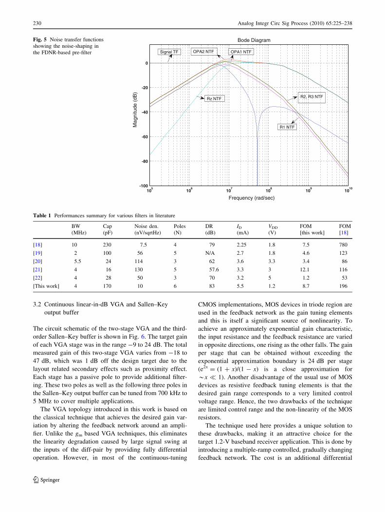
depends on the value of D and Rz. Figure 5 shows the
plots for the magnitude of noise transfer functions of the
various noise sources as well as the signal transfer function.
Since the noise generated by the FDNR resistors is shaped,
the designer can use larger resistors (noisier) and hence can
reduce the capacitor size. This again results in a significant
area saving. The total integrated in-band noise voltage can
be calculated as [5]:
VnT¼ fc � 2pRf C1=
ffiffiffi3ph i
�ffiffiffiffiffiffiffiffiffiffiffiffiffiffiffiffiffiffiffiffiffiffiffiffiffiffiffiffiffiffiffiffiffiffiffiffiffiffiffi
3 V2nRþ 2V2
namp
� �fc
r
¼ a � Vnthermal tot ð12Þ
Thus, one can see that the total noise generated by
the filter components is reduced by the factor a ¼½fc � 2pRf C1=
ffiffiffi3p�: The value of Rf is determined by the
pass-band gain of the mixer, while fc is the filter 1-dB
cutoff frequency. Therefore, the only design parameter
available for noise shaping is the value of the capacitor
C1. Clearly, C1 should be minimized to obtain better noise
performance. The minimum value for C1 is limited by the
maximum op-amp output swing at the internal FDNR
nodes.
This noise shaped filtering idea is also utilized in the
following high input impedance instrumentation type PMA
stage (Fig. 3). An asymmetric floating frequency depen-
dent negative resistance (AFFDNR) feedback structure is
introduced, to simultaneously provide both gain and fil-
tering. Avoiding the amplification of the blockers both
relaxes the linearity requirement of the amplifier and
relieves the filtering requirements of the following stages.
This time the feedback gain resistor Rfb is reutilized, and
the noise of the AFFDNR circuit elements in the feedback
path is shaped, and hence, once more, the desired third-
order elliptic filtering is obtained without any significant
noise degradation. It should be noted that the proposed
AFFDNR is not a reciprocal circuit and that the mentioned
filtering action can only be obtained provided that the
polarity is as shown in Fig. 3. Specifically as shown in the
inset in Fig. 3, the impedance looking into the node A, ZA,
is negative with node B grounded, whereas, the impedance
looking into the node B, ZB, is inductive when node A is at
ground. Depending on the signal strength in the band of
interest, the gain of the PMA stage can be adjusted and is
2-bit programmable to be 20-, 15-, 8-, or 0-dB. Rin is used
to set the gain without affecting the cut-off and notch
response of the circuit. In the 0-dB gain mode, the AFFDNR
circuit is powered down to save power.
The input referred noise density of this combination
is 10 and 14 nV/sqrtHz in DVB-H and ISDB-T modes
respectively. This section consumes a die area of
0.28 mm2. In ISDB-T full-gain mode, 2.4- and 4.4-MHz
blockers (3.5 dBm each) result in -59.6-dBm IM3 product
which corresponds to an out-of-band IIP3 of 44.5 dBm. In-
band IIP3 for this case is 18 dBm. In DVB-H mode, 5- and
8-MHz blockers (3.5 dBm each) result in -55-dBm IM3
which corresponds to an out-of-band IIP3 of 42.6 dBm. In-
band IIP3 for DVB-H case is 15.5 dBm. The pre-filter
consumes 2.6 mA from a 1.2-V supply, while the PMA
needs 3.9 mA in full-gain mode from the same 1.2-V
supply.
The figure of merit (FOM) defined in [18] and perfor-
mance metrics from which the FOM is calculated are
summarized in Table 1. This FOM however neglects the
die area as a performance factor. Hence we define and also
show in Table 1 a simple figure of merit (FOM) that
compares the performance of this pre-filter-PMA section
with the other filters in the literature that incorporates the
area tradeoff. The FOM proposed in this work is as
follows:
FOM ¼ ðDR � BWÞ=VDD
BW � Ctotð Þ=Nð Þ � Pwrð Þ= N � BWð Þð Þ ð13Þ
where DR is dynamic range, BW is the filter bandwidth,
Ctot is the total amount of capacitance used, Pwr is the
power consumption and N is the number of poles. This
FOM includes dynamic range as well as the required power
consumption and total capacitance, scaling them with
respect to the filter bandwidth and number of poles.
3 4 5 6 70
2
4
6
8
10
12
14
16
18
20
Noise Density [nV/sqrtHz]
PM
A c
urre
nt [m
A]
Fig. 4 PMA noise density versus required current consumption
Analog Integr Circ Sig Process (2010) 65:225–238 229
123
Page 6
3.2 Continuous linear-in-dB VGA and Sallen–Key
output buffer
The circuit schematic of the two-stage VGA and the third-
order Sallen–Key buffer is shown in Fig. 6. The target gain
of each VGA stage was in the range -9 to 24 dB. The total
measured gain of this two-stage VGA varies from -18 to
47 dB, which was 1 dB off the design target due to the
layout related secondary effects such as proximity effect.
Each stage has a passive pole to provide additional filter-
ing. These two poles as well as the following three poles in
the Sallen–Key output buffer can be tuned from 700 kHz to
5 MHz to cover multiple applications.
The VGA topology introduced in this work is based on
the classical technique that achieves the desired gain var-
iation by altering the feedback network around an ampli-
fier. Unlike the gm based VGA techniques, this eliminates
the linearity degradation caused by large signal swing at
the inputs of the diff-pair by providing fully differential
operation. However, in most of the continuous-tuning
CMOS implementations, MOS devices in triode region are
used in the feedback network as the gain tuning elements
and this is itself a significant source of nonlinearity. To
achieve an approximately exponential gain characteristic,
the input resistance and the feedback resistance are varied
in opposite directions, one rising as the other falls. The gain
per stage that can be obtained without exceeding the
exponential approximation boundary is 24 dB per stage
(e2x = (1 ? x)/(1 - x) is a close approximation for
*x � 1). Another disadvantage of the usual use of MOS
devices as resistive feedback tuning elements is that the
desired gain range corresponds to a very limited control
voltage range. Hence, the two drawbacks of the technique
are limited control range and the non-linearity of the MOS
resistors.
The technique used here provides a unique solution to
these drawbacks, making it an attractive choice for the
target 1.2-V baseband receiver application. This is done by
introducing a multiple-ramp controlled, gradually changing
feedback network. The cost is an additional differential
105
106
107
108
109
1010
-100
-80
-60
-40
-20
0
Mag
nitu
de (
dB)
Bode Diagram
Frequency (rad/sec)
Signal TF OPA2 NTF OPA1 NTF
Rz NTF
R1 NTF
R2, R3 NTF
Fig. 5 Noise transfer functions
showing the noise-shaping in
the FDNR-based pre-filter
Table 1 Performances summary for various filters in literature
BW
(MHz)
Cap
(pF)
Noise den.
(nV/sqrtHz)
Poles
(N)
DR
(dB)
ID
(mA)
VDD
(V)
FOM
[this work]
FOM
[18]
[18] 10 230 7.5 4 79 2.25 1.8 7.5 780
[19] 2 100 56 5 N/A 2.7 1.8 4.6 123
[20] 5.5 24 114 3 62 3.6 3.3 3.4 86
[21] 4 16 130 5 57.6 3.3 3 12.1 116
[22] 4 28 50 3 70 3.2 5 1.2 53
[This work] 4 170 10 6 83 5.5 1.2 8.7 196
230 Analog Integr Circ Sig Process (2010) 65:225–238
123
Page 7
voltage ramp circuit which leads to only a slight increase in
area and power. The schematic of one of these stages with
complementary control ramps is shown in Fig. 7. With
increasing AGC control voltage, the control voltages of the
input resistors rise, while the control voltages on the
feedback resistors decrease, increasing the closed loop
amplifier gain approximately exponentially. For a particu-
lar gain setting, most of the switches are completely on or
Vcn[1:N] Vcn[1:N]
Ramp Gen.
VGAamp VGAamp
VctrAGC
Vin
Vcp[1:N] Vcp[1:N]
R1p
R1n
SKamp
SKamp
Vout
R2n
R3p
R3n
R4n
R5p
R5n
R6p
R6n
R7n
R7p
C1 C2
C3p
C3n
R2p R4p
Single pole, -9dB to 24dB variable gain
Single pole, -9dB to 24dB variable gain
Three anti-aliasing poles, 0dB gain
BW Trim
Fig. 6 Schematic of the back-end chain including the two-stage VGA and the third-order Sallen–Key buffer
Amp.
Ramp Gen.VctrAGC
Vcp[1:N]
Vcn[1:N]
Vin Vout
R1
RMR2
RMR2
RMR2
RMR2
Vc1
Vc2
Vc3
VcN
VctrAGC
Vsw
VcpNVcp1Vcp2
Vcn1Vcn2 VcnN
Vc[1:N]
R1
RMR2
RMR2
RMR2
RMR2
Vc1
Vc2
Vc3
VcN
Vc[1:N]
BA
A B
A B
A B
C1
C2
C2
C2
C2
(a)
(b)
Fig. 7 a Schematic of the proposed fully differential ramp-based VGA stage. b Differential ramp control voltages versus AGC control voltage
M1 M2
II
VctrAGCVref R1
R2 R2 R2R2
Ib 2Ib
Vcp1 Vcp2 Vcp3 VcpN
2-bit slope ctr
VcnN
R2 R2 R2 R2
Vcn1Vcn2Vcn3
Ib2Ib(N-1)Ib (N-1)Ib
Fig. 8 Schematic of the differential ramp voltage circuit
Analog Integr Circ Sig Process (2010) 65:225–238 231
123
Page 8
off causing no linearity degradation. Only a few of these
switches are in their mid-range and so with careful design
the non-linearity contribution of these can be insignificant.
The question then becomes: how many unit elements are
needed to attain the desired linearity?
The differential ramp voltage generation circuit is
shown in Fig. 8. The input AGC control voltage is com-
pared with a reference voltage Vref and the difference
current running through R1 causes the current in one of the
diode connected devices to increase and the current
through the other one to decrease. By mirroring this current
into a resistor, a control voltage proportional to the input
voltage difference can be obtained. Multiple control volt-
ages with the desired amount of offset are obtained by
simply pulling fixed amount of offset current from each of
these mirrored branches. The ramp voltage VcpN, for
example, can be written down as follows:
VcpN ¼ VctrAGC � Vrefð ÞR2
R1
� ðN � 1ÞIbð Þ � R2: ð14Þ
The resistor ratio in the first term, (R2/R1), defines the
slope of the characteristics, whereas the second term is the
ctr5 ctr4 ctr3 ctr2 ctr1 ctr0
p n
Ibias
M50
R2R4R8R32R 16RR
R2b
R1b
M52
M51
M49
2R 4R 8R 16R 32R
M53 M54
R1a
R2a ctr0b ctr1b ctr2b ctr3b ctr4b ctr5b
Vcm
Ibias
Cal_clkDCOCCorrection
DCOC trim codeSuccessive
approx.Logic
p n
Vin+ Vin-M1 M2
M3 M4
M5 M6
M7
M8
M9 M10M11M12 M13
M14
M15 M16
M17 M18
M20 M21 M23M22
(a)
(b)
Fig. 9 a Schematic of the class-A VGA amplifier with dc-offset control (DCOC). b DCOC correction circuit
0.6 0.8 1 1.2 1.4 1.6 1.8 2-40
-30
-20
-10
0
10
20
30
40
50
60
Control Voltage [V]
Gai
n [d
B]
1 1.1 1.2 1.3 1.4 1.5 1.6 1.7-4
-3
-2
-1
0
1
2
3
4
Control Voltage [V]
Gai
n E
rror
[dB
]
0.8dB
(b)(a)
measured
ideal
Fig. 10 a The measured gain characteristics for the nominal slope setting. b The gain error curve for the same nominal slope setting
232 Analog Integr Circ Sig Process (2010) 65:225–238
123
Page 9
fixed offset. In order to have flexibility in the design, R1 is
trimmable with two-bit slope control word enabling
adjustment of the slope of the control ramps and hence
the VGA characteristics.
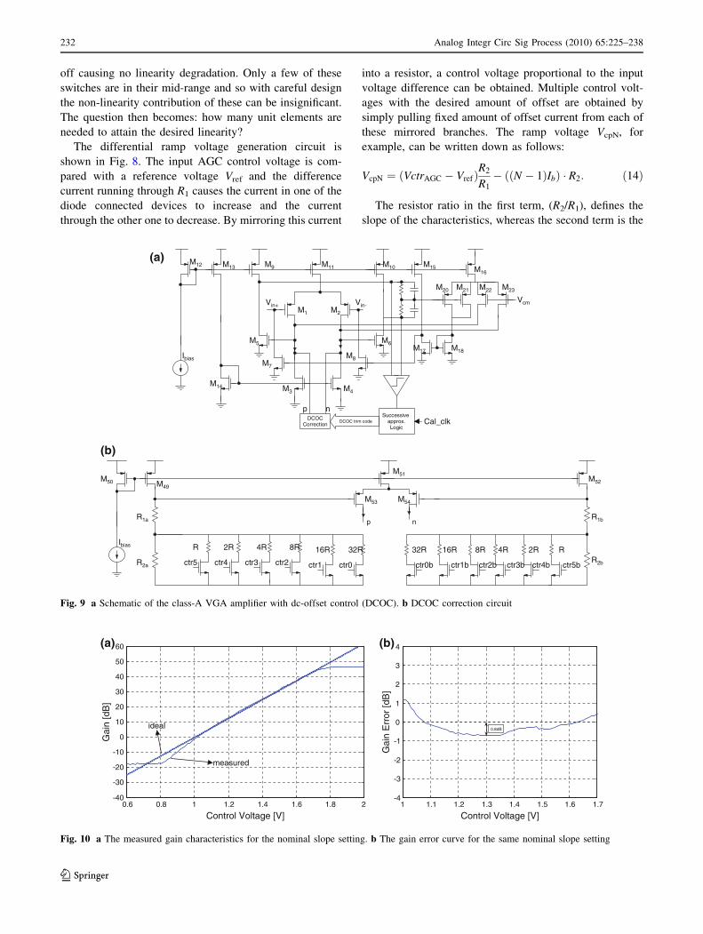
The fully differential class-A VGA amplifier with DC
offset calibration (DCOC) is shown in Fig. 9. When the
chip is powered up, the inputs to the first gain stage in the
baseband chain are shorted and then starting with this stage
every gain stage is subsequently calibrated to remove any
DC offset. To ensure the smallest residual DC offset each
amplifier is set to its maximum gain during this procedure.
Once the calibration of all the blocks is complete, the
design switches into the normal mode of operation. The
VGA amplifier is a two stage, fully differential Miller-
compensated opamp with a unity gain bandwidth greater
than 250-MHz. A phase margin of 70� is allocated for both
common-mode and differential-mode loops. The PMOS
devices, M22 and M23, compare the common-mode level
with the desired reference level, and to set the output
common-mode voltage this feedback loop injects the
proper amount of current into the differential output nodes
of the first stage. During the start-up, to eliminate the
possibility of the inputs and outputs of the amplifier
latching-up to VDD, a small bleed current is applied
through M15, causing the very weak NMOS devices M7
and M8 turn-on and pull down the amplifier inputs. After
Comp
Ccode
RtrimSARLogic
main_reset
Comp
reset
dff
rst
q
ck
d
main_reset
sec_reset
code_outdff
rst
q
ck
d
dff
rst
q
ck
d
dff
rst
q
ck
d
main_reset
main_reset
fdnr_code<0>
fdnr_code<5>
fdnr_code<4>
done
Out_code
Cal_Engine
sw_mode MUX
MUX sw_mode
sw_mode
cal_done
main_reset
pass
hold_in
clk_pulse
main_reset
hold_in
clk_pulse
sec_reset
pass
sw_mode
cal_done
trimcode_1
trimcode_2
Bac
kend
_co
d
IREF*R = [IREF/(2*Fck)]/C∴C*R = 1/(2*Fck)
IREF*R
1/(2*Fck) 1/Fck
time
Fig. 11 The bandwidth calibration circuit and its timing diagram
Analog Integr Circ Sig Process (2010) 65:225–238 233
123
Page 10
the amplifier turns on and common mode levels are
reached, these devices turn off.
The DCOC circuits are also included in the amplifier
schematic (Fig. 9(a)). During the calibration sequence, a
comparator detects any DC offset at the differential out-
puts. Depending of the polarity of the offset, a successive
approximation engine updates the six-bit trim code reduc-
ing the amount of offset error in every cycle. At the end of
six cycles, the resultant six-bit trim code is latched and the
‘‘calibration done’’ signal is flagged. The DCOC correction
circuit is shown in Fig. 9(b). Depending on the polarity of
the offset, the circuit injects a differential current into the
output nodes of the first stage, balancing the offset. The
input referred offset correction range is 20 mV per VGA.
The maximum level of offset that can occur at any point
along the chain is limited by comparator accuracy to
2–3 mV.
The output buffer which drives the off-chip load is a
class-AB amplifier in a third-order Sallen–Key (SK) con-
figuration. This buffer configuration is preferred for two
main reasons. First, the additional third-order filtering
serves as the anti-aliasing filter for the following data
converter stage, and prevents the SNR degradation due to
aliasing. Second, because of the two-path feedback, the
amount of compensation required for this buffer is relaxed
allowing a wider bandwidth with no additional power.
Slight peaking is allowed in this stage to compensate for
the droop caused by the passive VGA poles. The class-AB
amplifier of the PMA is reused in this buffer stage with
only a slight change in the compensation network.
The measured VGA gain characteristics and the gain
error curve are shown in Fig. 10. In maximum gain con-
figuration, the measured in-band OIP3 corresponding to
3- and 4-MHz -48 dBm input tones is 22 dBm, whereas,
5- and 8-MHz N ? 1 blockers at a -50 dBm input level
results in a 34 dBm OIP3. The input referred in-band noise
density is 11 nV/sqrtHz for the VGA-SK combination. The
total die area of this section is 0.17 mm2. The block con-
sumes 2.65 mA of current from a 1.2-V supply and 200 lA
current from a 2.5-V supply for the switch control ramp
circuit.
3.3 Bandwidth calibration circuit
The bandwidth calibration circuit and its timing diagram
are shown in Fig. 11. During the initial calibration a 7-bit
bandwidth calibration code sets the resistive DAC targeting
the desired filter bandwidth for a given crystal clock fre-
quency. The trim range of this resistor is large enough to
cover whole filter bandwidth as well as any reference
crystal frequency in the range of 10–40 MHz. Following
this, successive approximation logic computes a calibration
code with the help of a comparator as illustrated in Fig. 11.
Note that, since the resistor in this configuration is used as
a trim element determining the bandwidth and crystal
frequency, the capacitor is used as the calibration element
with 6-bit resolution.
The first baseband stages (FDNR pre-filter and PMA)
require a different calibration code than the backend cir-
cuits. There are multiple ways to generate the two sets of
codes corresponding to different trim element ratios in the
different circuit blocks. One solution is to use two different
calibration circuits. Because of the extra die area required,
this solution is not an attractive one. A second solution is to
generate a code for one of the blocks and then use a digital
fractional multiplier to scale this code to generate the trim
codes required by the other block. Although, the area
penalty in this solution is much less, it still adds to the total
die area. Another solution, which is used in this design,
eliminates the area penalty completely. The idea is to run
the calibration sequence twice. After the first sequence the
first calibration code is latched into a register (FDNR
code). Following this, the capacitor ratios in the calibration
engine are reconfigured to generate another set of calibra-
tion codes for the backend blocks. A new set of resistor
trim codes is also switched into be able to set the poles of
the backend blocks independently. In this way, the overall
cut-off, notch and stop-band response of the whole chain
can be adjusted independently, offering a universal widely
tunable solution.
On the filter side, in addition to the 6-bit resolution
capacitor bank, there is a resistor trim to switch between
the high-end and the low-end of the bands. The tuning
resolution at the low-band mode is around 20 kHz while it
is 80 kHz in the high-band mode.
FDNRPRE-FILTER
VGA & SK BUF.
PMAAFFDNR
DIGITALADC
FDNR FILTER AND OTHER TEST CIRCUITS
Fig. 12 Die photo of the complete receiver baseband
234 Analog Integr Circ Sig Process (2010) 65:225–238
123
Page 11
Table 2 Performance summary
of various baseband blocksBlock Parameter Measurement
ISDB-T(700 kHz) DVB-H(3.8 MHz)
Pre-filter Die area 0.16 mm2
In-band IIP3 22.5 dBm 20.6 dBm
N ? 1 blocker IIP3 36.5 dBm 31.5 dBm
HD2 (@ -1 dBm input) -57 dB -59 dB
Input referred noise 7.5 nV/sqrtHz 7 nV/sqrtHz
Stop-band attenuation 12 dB 13 dB
Notch attenuation 18 dB 19 dB
Tuning range 700 kHz to 5.2 MHz
Tuning resolution 20 kHz 80 kHz
Current consumption 2.6 mA from 1.2 V
PMA Die area 0.12 mm2
Max. gain 20-dB
Min. gain 0-dB
Gain steps 5-dB
HD2 (@ 2 dBm output) -57.4 dB -60.5 dB
N ? 1 blocker IIP3 37 dBm 29.7 dBm
Input referred noise 9.5 nV/sqrtHz 14 nV/sqrtHz
Stop-band attenuation 18 dB 17 dB
Notch attenuation 31 dB 26 dB
Tuning range 700 kHz to 4.2 MHz
Tuning resolution 20 kHz 80 kHz
Current consumption 3.9 mA from 1.2 V
VGA-SK buffer Die area 0.17 mm2
Max. gain 47 dB
Min. gain -18 dB
Gain steps Continuous
In-band IIP3 -25 dBm (@max gain)
N ? 1 blocker IIP3 -13 dBm (@max gain)
HD2 (@ 0 dBm output) -44 dB (@max gain)
HD3 (@ 0 dBm output) -42 dB (@max gain)
Input referred noise 11 nV/sqrtHz
Stop-band attenuation 26 dB(@ 2.5 MHz) 16 dB (@ 8 MHz)
Tuning range 700 kHz to 5 MHz
Tuning resolution 20 kHz 80 kHz
Current consumption 2.44 mA from 1.2 V
0.2 mA from 2.5 V
Analog baseband Die area 0.45 mm2
Max. gain 67 dB
Min. gain -18 dB
Gain steps Continuous
N ? 1 blocker IIP3 24 dBm 24.2 dBm
Input referred noise 10.5 nV/sqrtHz 14.5 nV/sqrtHz
Stop-band attenuation 64 dB (@ 2.5 MHz) 42 dB (@ 8 MHz)
Notch attenuation 78 dB 55 dB
Tuning range 700 kHz to 5.2 MHz
Tuning resolution 20 kHz 80 kHz
DR (@HD3 = 40 dB) 87.2 dB 82 dB
Current consumption 9 mA from 1.2 V and 0.2 mA from 2.5 V
Analog Integr Circ Sig Process (2010) 65:225–238 235
123
Page 12
4 Experimental results
The proposed baseband architecture was implemented in a
65-nm CMOS process and tested. The die photo is shown in
Fig. 12. The inputs and outputs of various sub-blocks were
connected to pins to enable measurement of each section
separately. The parameters of various sections used in the
design are useful in illustrating the limitations of each
block. Table 2 summarizes the performance parameters of
the individual blocks and the whole baseband chain. The
105
106
-80
-60
-40
-20
0
20
40
60
80
Frequency [Hz]
Mag
nitu
de [d
B]
106
107
-60
-40
-20
0
20
40
60
80
Frequency [Hz]
Mag
nitu
de [d
B]
(b)(a)
Fig. 13 The measured baseband frequency response in: a ISDB-T mode and b DVB-H mode
105
106
-90
-80
-70
-60
-50
-40
-30
-20
-10
0
Frequency [Hz]
Out
put L
evel
[dB
m]
Tone1
Tone2
IM3
IM2
106
107
-80
-70
-60
-50
-40
-30
-20
-10
0
Frequency [Hz]
Out
put L
evel
s [d
Bm
]
Tone1
Tone2IM3 IM2
(a) (b)
Fig. 14 a Two-tone test in ISDB-T mode. b Two-tone test in DVB-H mode
(a)
-40 -30 -20 -10 0 10 20 30 40-120
-100
-80
-60
-40
-20
0
20
40
Input Level [dBm]
Out
put L
evel
s (in
put r
efer
red)
[dB
m]
IIP3 = 24.2 dBm
(b)
-20 -10 0 10 20 30 40-120
-100
-80
-60
-40
-20
0
20
40
Input Level [dBm]
Out
put L
evel
s [d
Bm
]
IIP3 = 24 dBm
Fig. 15 Measured IIP3: a in ISDB-T mode and b in DVB-H mode
236 Analog Integr Circ Sig Process (2010) 65:225–238
123
Page 13
frequency response of the analog baseband chain in ISDB-T
and DVB-T/H modes is shown in Fig. 13. 85-dB blocker-
aware continuous gain range combined with low-noise
operation results in 87.2 and 82.5 dB dynamic range in
ISDB-T and DVB-T/H modes, respectively. The two-tone
linearity measurements for N ? 1 blockers are conducted at
a gain of 56 dB. In ISDB-T mode, 2.4- and 4.4-MHz
blockers (-10 dBm each at the output) result in a -22-dBm
IM3 which corresponds to an out-of-band IIP3 of 24.2 dBm
(Fig. 14(a)). In DVB-H mode, 7- and 12-MHz blockers
(-15 dBm each at the output) result in a -38-dBm IM3
which corresponds to an out-of-band IIP3 of 24 dBm
(Fig. 14(b)). Figure 15 shows the measured IIP3 interpo-
lation data for the target bands. The chain achieves an input
referred noise level of 10.5 nV/sqrtHz. The measured input
referred noise plot is shown in Fig. 16. The entire receiver
baseband occupies a total die area of 0.45 mm2. The design
consumes total of 9 mA of current from a 1.2-V supply, as
well as, an additional 0.2 mA VGA ramp-control current
from a 2.5-V supply. Total power consumption is 11.5 mW.
5 Conclusion
A unique analog baseband chain approach is introduced to
mitigate the disadvantages incurred with the supply voltage
scaling required in a deep-sub-micron process. The per-
formance metrics of this design as well as other baseband
receivers in the literature are summarized in Table 3. This
approach provides comparable or superior performance for
certain metrics, relative to higher voltage alternatives,
without requiring the additional area needed for large
capacitors. The new techniques introduced, noise-shaped
blocker filtering and linear VGA operation with continuous
gain tuning, maximize the dynamic range of the radio. This
baseband receiver circuit when placed at the mixer output
allows a higher front-end gain, thus relaxing its noise
requirement. Measurements have been conducted for two
mobile-TV applications, ISDB-T and DVB-T/H but the
receiver can be tuned to suit any application in a frequency
band from 700 kHz to 5.2 MHz. The frequency response
can be configured to accommodate the blocker profile
appropriate for the desired application. The multiple cali-
bration sequences during the power-up provide multiple
trim codes for various blocks along the chain. Thus,
independent characteristics along the chain can be com-
bined to yield the best response for the desired application.
Acknowledgments Authors would like to thank all of the col-
leagues at Newport Media for their valuable contributions in the
design, layout and testing of the test-chip.
Open Access This article is distributed under the terms of the
Creative Commons Attribution Noncommercial License which per-
mits any noncommercial use, distribution, and reproduction in any
medium, provided the original author(s) and source are credited.
References
1. The International Electrotechnical Commission (IEC). Mobileand portable DVB-T radio access interface specification.MBRAI-02-16, version 1.0.
2. D’Amico, S., et al. (2008). A CMOS 5 nV/sqrtHz 74-dB-gain-
range 82-dB-DR multistandard baseband chain for bluetooth,
UMTS, and WLAN. IEEE Journal of Solid-State Circuits, 43(7),
1534–1541.
3. Antoine, P., et al. (2005). A direct-conversion receiver for DVB-
H. IEEE Journal of Solid-State Circuits, 40(12), 2536–2546.
4. Vassiliou, I., et al. (2008). A 65 nm CMOS multistandard, mul-
tiband TV tuner for mobile and multimedia applications. IEEEJournal of Solid-State Circuits, 43(7), 1522–1533.
5. Tekin, A., et al. (2008). Noise-shaping gain-filtering techniques
for integrated receivers. IEEE Journal of Solid-State Circuits,44(10), 2689–2701.
6. Elwan, H., et al. (2009). A differential ramp based 65 dB-linear
VGA technique in 65 nm CMOS. IEEE Journal of Solid-StateCircuits, 44(9), 2503–2514.
106
107
0
0.2
0.4
0.6
0.8
1
x 10-8
Frequency [Hz]
Noi
se D
ensi
ty [V
/sqr
tHz]
Fig. 16 Total input referred noise
Table 3 Performance comparison of various receiver baseband in the
literature
Features [7] [8] [2] [This
work]
Bandwidth (MHz) 1 1 2.2 3.8
Technology
(CMOS)
1.2 lm 0.18 lm 130 nm 65 nm
Supply (V) 3.0 1.8 2.5 1.2
Power (mW) 7.1 4.86 20.5 11.5
Gain Range (dB) 12 to 30 12 to 55 -6 to 68 -18 to 67
Gain Step (dB) 6 2 10 Continuous
DR (dB) @ -
40 dB HD3
60.1
(SFDR)
73.5
(SFDR)
82 (11 MHz
BW)
82.5
IIP3 (dBm) 12.2 30 21 24
IRN (nV/sqrtHz) 43.2 32 5 10.5
Die area (mm2) 2.89 1.5 1.65 0.45
Analog Integr Circ Sig Process (2010) 65:225–238 237
123
Page 14
7. Elwan, H. O., et al. (2002). A buffer-based baseband analog front
end for CMOS bluetooth receivers. IEEE Transactions on Circuitsand Systems, 49(8), 545–554.
8. Lee, M., et al. (2004). An integrated low power CMOS baseband
analog design for direct conversion receiver. In Proceedings ofthe 30th European solid-state conference (pp. 79–82), September
2004.
9. Saias, D., et al. (2005). A 0.12 lm CMOS DVB-T tuner. ISSCCDig. Tech. Papers, pp. 430–431, Feb. 2005.
10. Dawkins, M., et al. (2003). A single chip tuner for DVB-T. IEEEJournal of Solid-State Circuits, 38, 1307–1317.
11. Connell, L., et al. (2002). A CMOS broadband tuner IC. ISSCCDig. Tech. Papers, pp. 400–401, Feb. 2002.
12. D’Amico, S., et al. A 6.4 mW, 4.9 nV/sqrtHz, 24 dBm IIP3 VGA
for a multi-standard (WLAN, UMTS, GSM, and Bluetooth)
receiver. IEEE ESSCIRC06, pp. 82–85.
13. Antoniou, A. (1969). Realisation of gyrators using operational
amplifiers, and their use in RC-active network synthesis. IEEEProceedings, 116(11), 1838–1850.
14. Antoniou, A. (1971). Bandpass transformation and realization
using frequency-dependent negative resistance elements. IEEETransactions on Circuit Theory, CT-18, 297–299.
15. Bruton, L. T. (1969). Network transfer functions using the con-
cept of frequency dependent negative resistance. IEEE Transac-tions on Circuit Theory, CT-16, 406–408.
16. Martin, K., et al. (1977). Optimum design of active filters using
the generalized immitance converter. IEEE Transactions onCircuits and Systems, CAS-24, 495–502.
17. Hutchison, J., et al. (1981). Some notes on practical FDNR filters.
IEEE Transactions on Circuits and Systems, CAS-28(3),
242–245.
18. D’Amico, S., et al. (2006). A 4.1-mW 10-MHz fourth-order
source-follower based continuous-time filter with 79-dB DR.
IEEE Journal of Solid-State Circuits, 41(12), 2713–2719.
19. Yoshizawa, A., et al. (2007). A channel-select filter with agile
blocker detection and adaptive power dissipation. IEEE Journalof Solid-State Circuits, 42(5), 1090–1099.
20. Mensink, C. H. J., et al. (1997). A CMOS ‘‘soft-switched’’
transconductor and its application in gain control and filters.
IEEE Journal of Solid-State Circuits, 32(7), 989–998.
21. Yoo, C., et al. (1998). A ± 1.5-V 4-MHz CMOS continuous-time
filter with single-integrator based tuning. IEEE Journal of Solid-State Circuits, 33(1), 18–27.
22. Krummanecher, F., et al. (1988). A 4-MHz CMOS continuous-
time filter with on-chip automatic tuning. IEEE Journal of Solid-State Circuits, 23(3), 750–758.
Ahmet Tekin received his B.S.
degree in EE from Bogazici
University, Istanbul, Turkey,
M.S. degree in EE from North
Carolina A&T State University,
NC and Ph.D. degree from UC
Santa Cruz, CA in 2002, 2004,
and 2008, respectively. He was
research assistant at RF Micro-
electronics Lab at North Caro-
lina A&T State University from
2002 to 2004 and at Bio-
Mimetic Microelectronic Sys-
tems Lab at UC Santa Cruz
from 2004 to 2005 focusing on
low power Analog-RF circuit design. He was with Multigig Inc., CA,
from 2005 to 2007, and with Newport Media Inc., CA from 2007 to
2009 working on various Analog-RF CMOS data conversion and
wireless transceiver circuits. He is currently with Aydeekay LLC, CA,
focusing on CMOS Analog-RF circuits for automotive applications.
Hassan Elwan was born in
Cairo, Egypt, in 1971. He
received the B.Sc. and M.Sc.
degrees from Cairo University
in 1994 and 1996, respectively.
He received his Ph.D. degree
from The Ohio State University
in 2001. He joined Silicon
Laboratories wireless division
from 2002 to 2005 where he
designed various circuits for
GSM wireless transceivers and
SoC’s. In 2005 He joined
Newport Media Inc. where he is
currently the design manager of
the analog and mixed signal group. Dr. Elwan research interests
include mixed signal CMOS circuit design, power management and
data convertors.
Kenneth Pedrotti received the
B.S. degree in Engineering
Physics in 1978 and M.S.
degree in Quantum Electronics
in 1979 from the University of
California at Berkeley and the
Ph.D. degree in Electrical
Engineering, in 1985, from
Stanford University. Currently
he is a professor and chairman
of the Department of Electrical
Engineering at the University of
California at Santa Cruz. His
interests include devices and
circuits for optical communica-
tion networks, RF, biomedical applications, energy scavenging and
imaging. From 1998 to 2000 he was with the Rockwell Science
Center in Thousand Oaks, CA working on mixed signal VLSI for
visible and IR imaging. Prior to that he worked from 1997 to 1998 for
Rockwell Semiconductor Systems in Newbury Park, CA on integrated
circuits for optical communications. From 1985 to 1997 he was with
the Rockwell Science Center, his research activities there included the
development of integrated optoelectronic devices and circuits, high
speed circuit development using AlGaAs-GaAs heterojunction bipo-
lar transistors, systems research for WDM optical networks, optical
modulators, quantum well lasers, vertical cavity surface emitting
lasers and MOCVD crystal growth. Dr. Pedrotti has served on the
board of governors of the IEEE Solid State Circuit Society, as asso-
ciate editor of the IEEE Transactions on Circuits and Systems, has
authored over 80 publications and holds 11 patents.
238 Analog Integr Circ Sig Process (2010) 65:225–238
123