HAL Id: hal-01515990 https://hal.inria.fr/hal-01515990 Submitted on 28 Apr 2017 HAL is a multi-disciplinary open access archive for the deposit and dissemination of sci- entific research documents, whether they are pub- lished or not. The documents may come from teaching and research institutions in France or abroad, or from public or private research centers. L’archive ouverte pluridisciplinaire HAL, est destinée au dépôt et à la diffusion de documents scientifiques de niveau recherche, publiés ou non, émanant des établissements d’enseignement et de recherche français ou étrangers, des laboratoires publics ou privés. Distributed under a Creative Commons Attribution| 4.0 International License Design and Optimization of a Digital Baseband Receiver ASIC for GSM/EDGE Christian Benkeser, Qiuting Huang To cite this version: Christian Benkeser, Qiuting Huang. Design and Optimization of a Digital Baseband Receiver ASIC for GSM/EDGE. 18th International Conference on Very Large Scale Integration (VLSISOC), Sep 2010, Madrid, Spain. pp.100-127, 10.1007/978-3-642-28566-0_5. hal-01515990
Transcript
HAL Id: hal-01515990https://hal.inria.fr/hal-01515990
Submitted on 28 Apr 2017
HAL is a multi-disciplinary open accessarchive for the deposit and dissemination of sci-entific research documents, whether they are pub-lished or not. The documents may come fromteaching and research institutions in France orabroad, or from public or private research centers.
L’archive ouverte pluridisciplinaire HAL, estdestinée au dépôt et à la diffusion de documentsscientifiques de niveau recherche, publiés ou non,émanant des établissements d’enseignement et derecherche français ou étrangers, des laboratoirespublics ou privés.
Distributed under a Creative Commons Attribution| 4.0 International License
Design and Optimization of a Digital Baseband ReceiverASIC for GSM/EDGE
Christian Benkeser, Qiuting Huang
To cite this version:Christian Benkeser, Qiuting Huang. Design and Optimization of a Digital Baseband Receiver ASICfor GSM/EDGE. 18th International Conference on Very Large Scale Integration (VLSISOC), Sep2010, Madrid, Spain. pp.100-127, �10.1007/978-3-642-28566-0_5�. �hal-01515990�
Abstract. This paper addresses complexity issues at algorithmic andarchitectural level of digital baseband receiver ASIC design for the stan-dards GSM/GPRS/EDGE, in order to reduce power consumption anddie area as desired for cellular applications. To this end, the hardwareimplementation of a channel shortening pre-filter combined with a de-layed decision-feedback sequence estimator (DFSE) for channel equal-ization is described. The digital receiver back-end including a flexibleViterbi decoder implementation is presented and hardware savings thatcan be achieved by using hard-decisions are discussed. Design trade-offsare highlighted to prove the efficiency of the implemented 2.5G multi-mode architecture. The ASIC in 0.13µm CMOS technology occupies1.0mm2 and dissipates only 1.3mW in fastest EDGE data transmissionmode.
Cellular wireless communications has changed our lives in the past 20 years.Today, with 3.5 billion subscribers [1] the far most important cellular communi-cation system GSM is used by all sorts of people all around the world. Simple 2Gdata communication is possible with the standard extension GPRS, but gooduser experience during wireless web-browsing and other non-voice applicationscan only be achieved since 2.5G EDGE data-services have been introduced.
EDGE increases 2G peak data rates to 240 kbps, mainly due to a highermodulation order (8PSK) and stronger channel coding. The symbol rate of270 kbps is identical with basic GSM, but 8PSK modulation improves the spec-tral efficiency, which comes at the cost of receiver complexity. Especially channel
2
equalization and symbol demodulation is a challenging task in EDGE, and re-quires sophisticated low-complexity solutions to preserve the power-advantageand cost-advantage of 2G receivers. Although basic GSM can be implementedon advanced signal processors with tolerable power-levels today, EDGE requiresefficient ASIC accelerators to reduce the power consumption to the required levelin modern cellular phones.
In basic GSM with GMSK modulation typically the (optimum) Maximum-Likelihood Sequence-Estimator (MLSE) is used for channel equalization and de-modulation. The complexity of an MLSE algorithm for 8PSK signals, however,would even exceed what can be implemented on ASICs. Therefore, in recentyears a lot of work on channel equalization for EDGE has been performed. Ithas been shown that sub-optimum variants of the MLSE algorithm with ac-ceptable computational complexity, like reduced-state sequence estimation [2] ordecision-feedback sequence estimation [3], are suitable for channel equalizationof 8PSK modulated EDGE signals (e.g., [4,5]). Turbo equalization has also beendiscussed [6] and proposed as a solution for EDGE [7]. However, all these ex-plorations are simulation-based system analyses where implementation aspectsand crucial design metrics like power consumption are not considered. Further,a practical multi-mode solution supporting GMSK as well as 8PSK modulationhas not been treated so far.
This work describes the design of a low-power and low-cost digital basebandreceiver for GSM/GPRS/EDGE with focus on the most challenging block, thechannel equalization. The entire receiver chain has been mapped to dedicatedhardware in order to achieve best design metrics. Hardware realizations for keycomponents of the receiver ASIC realization have been optimized to providethe flexibility required for the specified modulation types and coding schemes.Costly hardware resources are shared to keep the silicon area low, and algorith-mic/architectural optimizations have been applied to achieve very low powerconsumption.
1.1 Outline
The paper is organized as follows. In Section 2 the GSM baseband transmitterand channel model are introduced. In Section 3 the high-level architecture ofthe receiver ASIC realized in this work is presented. Section 4 describes theimplemented channel equalizer solution in detail. In Section 5 the implementedchannel decoder solution is explained together with an analysis of the impactof hard-/soft-decision equalizer outputs on receiver implementation complexity.Measurement results and key figures of the receiver ASIC implementation arepresented in Section 6. The paper is concluded in Section 7.
2 System Overview
Fig. 1 shows the GSM/EDGE baseband transceiver system model used in thiswork. On the transmitter side the input data is first encoded with a convolutional
3
ChannelEncoding
Mapping
MultipathAWGN
Channel ChannelEstimation
ChannelEqualization
Block De-Interleaving
ChannelDecoding
Burst De-Interleaving
Original Data Received Data
DigitalBaseband
Receiver
BasebandTransmitPath
De-mapping
PuncturingDe-
Puncturing
Baseband Modelfor GSM/EDGE System
OverallCommunication
Channel
BlockInterleaving
PulseShaping
CIR
DFSE
TS
BurstInterleaving
Fig. 1. System model of the GSM/EDGE baseband transceiver model.
encoder (rate 1/2 for GSM/GPRS or rate 1/3 for the coding schemes specifiedfor EDGE). Then, selected bits are removed in the puncturing unit to adjustthe code rate as required for the specific transmission mode. After that, theorder of bits is scrambled in the block interleaver to distribute radio blocks ofup to 1184 bits across 4 or 8 bursts3. The resulting bits (information bits) aremapped in interleaved order on bursts with a length of 156.25 symbols (3 bits persymbol in 8PSK mode), which includes fixed tail bits for channel equalization,a fixed training sequence (TS) for channel estimation and a guard period4 asshown in Fig. 2. Finally, in the symbol mapper and pulse shaping filter thebursts are GMSK or 8PSK modulated with a symbol period of Ts = 3.69µs as
3 Depending on the specific modulation and coding scheme the bits can be interleavedover 4 or 8 bursts [8].
4 The guard period of 8.25 symbols ensures that subsequent bursts do not interferewith each other due to inter-symbol interference.
4
specified [9]. Typically the bursts are transmitted every 8 time slots as indicatedin Fig. 2 according to the time division multiple access scheme defined for GSM,and the remaining 7 slots are reserved for other users. However, several slots canbe reserved for data traffic of a single user in high-speed EDGE data transmissionmodes.
1 2 3 4 5 6 7 8
Information Symbols58
Information Symbols58
TS26
TB13
TB23
GP8.25
1 time slot = 156.25 symbols (0.577ms)
1 TDMA time frame
1 2 3 4 5 6 ...... 7 8
= 8 time slots (4.615ms)
TB: Tail Bits TS: Training Sequence GP: Guard Period
stealing flags
Fig. 2. Time division multiple access and the normal burst in GSM.
The bursts are submitted through a multipath communication channel withadditive white Gaussian noise (AWGN). The GSM test channel profiles [10] havea delay spread of up to 5Ts, causing considerable inter symbol interference (ISI).Even more ISI is introduced by the system itself, because the GSM channelbandwidth of 200 kHz is significantly lower than the symbol rate. Therefore,an overall communication channel with a delay spread of up to 8Ts has to beconsidered when removing ISI in the receiver with the channel equalizer.
3 Digital Baseband Receiver
The complete receive chain shown in Fig. 1 has been implemented in our ASIC.As indicated in the corresponding simplified block-diagram (Fig. 3) two 2.5 kbRAMs allow the buffering of up to 2 GSM bursts, each comprising the in-phaseand quadrature-phase component of 156 symbols. Each time a new GSM bursthas been received the channel impulse response (CIR) is estimated with thetraining sequence by using the Least Squares technique [11]. The ISI of unknowndata symbols adjacent to the training sequence causes estimation errors whenconsidering all 26 symbols of TS. In our implementation only the central 16symbols of TS are used to estimate the CIR. Since linear 8PSK modulation canbe realized with simple FIR filtering in the transmitter, the CIR of the overallcommunication channel including the pulse shaping filter can be estimated atthe receiver (cf., Fig. 1). In (non-linear) GMSK instead, the signal is modulatedindirectly by filtering and accumulating the phase. Hence, the transmitter pulseshaping cannot simply be included in the estimated CIR.
5
channel
estim
ation
pre
-filt
er
coeffic
ients
com
puta
tion
channel
equaliz
ation
input
buffering
pre
-filt
ering
RA
M
channel
decodin
g
flexib
le
64-s
tate
Viterb
i
decoder
FIR
pre
-filt
er
RA
M
8-s
tate
DF
SE
for
GS
MK
and 8
PS
K
Least-
Square
s
estim
ato
r
RA
M
com
ple
x-v
alu
ed s
ignals
bit-s
tream
mem
ory
addre
ss s
ignal
RA
M
TS
CIR
configura
tion
of 15 d
iffe
rent
modula
tion a
nd
codin
g s
chem
es
configura
tion
decoded
de-inte
rleavin
g
and d
e-p
unctu
ring
addre
ss
genera
tor
addre
ss
genera
tor
addre
ss
genera
tor
RA
M
de-inte
rleaver
mem
ory
channel decoder
input m
em
ory
bits
receiv
ed
sam
ple
s
filtere
d C
IR
Fig. 3. GSM/EDGE receiver ASIC block diagram.
6
Channel equalization and demodulation are performed in our receiver im-plementation with the combination of a minimum-phase FIR pre-filter and aDecision-Feedback Sequence Estimator (DFSE) which are explained in detailin Section 4. The pre-filter coefficients computed with the estimated CIR arebuffered to be used to filter the CIR and the stream of received samples. Theseare fed into the DFSE for channel equalization and demodulation.
High-speed EDGE transmission modes require continuous burst reception,because more than one burst can be allocated to a specific user in each timeframe. Therefore, the demodulation of each burst has to be finished in one burstperiod of Tb = 577µs. When a radio block (4 or 8 bursts) has been demod-ulated, the de-interleaver can begin to reorder the bits. Both, burst and blockde-interleaving are performed by generating the specific RAM addresses for writ-ing to and reading from the de-interleaver memory. The de-puncturing unit in-troduces zeros (no a-priori information on the demodulated symbol) into thedata stream to provide data blocks to the channel decoder with the correct coderate. A flexible Viterbi decoder for trellises with up to 64 states has been imple-mented to support 15 specified coding schemes. The channel decoder processesall branches in parallel to keep the receiver latency low.
4 A Combined Pre-filter and DFSE Solution
In an MLSE, as can be used for optimum equalization in GSM, all possible sym-bol combinations of length L that could have been transmitted are generated asreference symbol sequences. These sequences are modulated and convolved withthe CIR to emulate the effect of ISI. The resulting reference signals are comparedwith the received samples to generate branch metrics which are a measure forthe likelihood that the specific symbol sequence has been transmitted, given thereceived signal. The branch metrics are used by the Viterbi algorithm in a trellisdiagram to find the most probable transmitted symbols. Contrary to implemen-tations of Viterbi decoders, the branch metric generation is the most challengingpart in an MLSE. The computational complexity can be characterized with thenumber of trellis branches B = ML to be processed, where M denotes the mod-ulation order (alphabet size) with M = 1 for GMSK and M = 3 for 8PSK. Thelength of the reference symbol sequences L defines the maximum tap delay (delayspread) in the channel profile that is considered in the equalization. The storagerequirements are defined by the number of states in each trellis stage accordingto S = ML−1. When considering the impact of 7 previously transmitted sym-bols, i.e. L = 8, as required for GSM (cf., Section 2), the MLSE trellis is largein the GMSK case, and even beyond what can be realized with any hardwareplatform when processing 8PSK signals.
Contrary to the MLSE algorithm, in the DFSE not all possible symbol com-binations of the reference sequence are used for the comparison with the re-ceived samples. Decisions of the Viterbi algorithm on previous symbols, so-calledper-survivor estimates, are taken as fixed assumptions to reduce the number ofbranch metrics to be computed. Only the permutations of the firstD symbols are
7
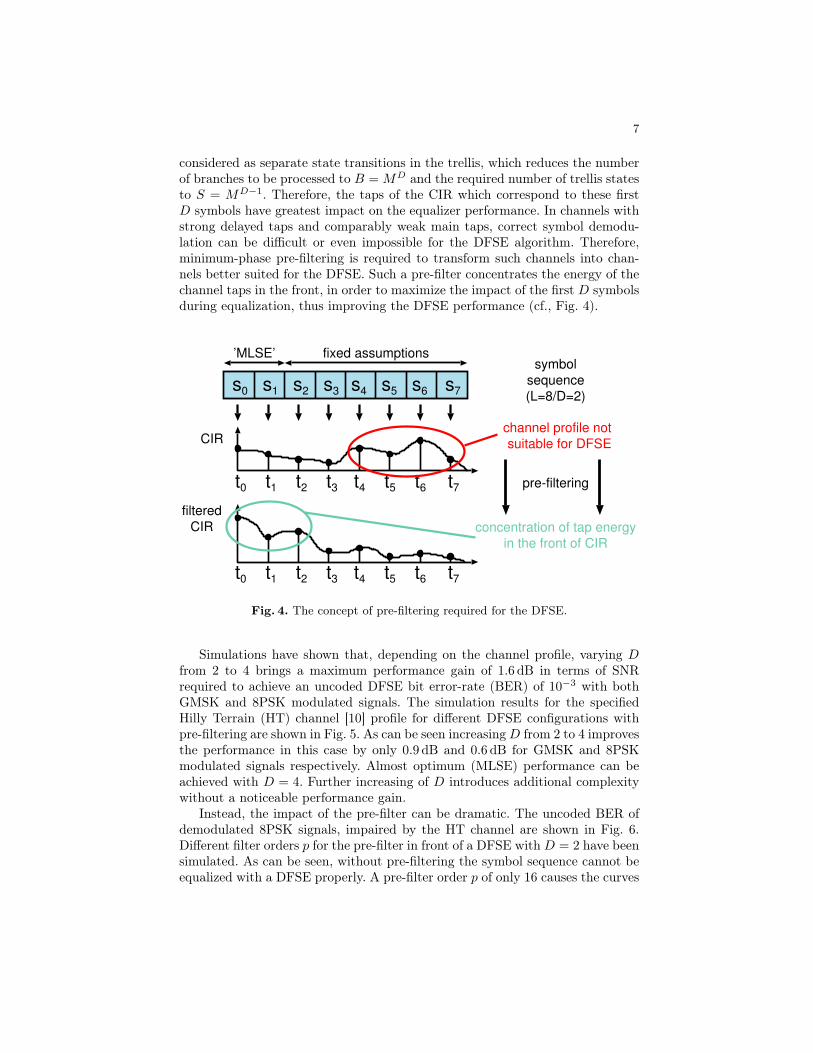
considered as separate state transitions in the trellis, which reduces the numberof branches to be processed to B = MD and the required number of trellis statesto S = MD−1. Therefore, the taps of the CIR which correspond to these firstD symbols have greatest impact on the equalizer performance. In channels withstrong delayed taps and comparably weak main taps, correct symbol demodu-lation can be difficult or even impossible for the DFSE algorithm. Therefore,minimum-phase pre-filtering is required to transform such channels into chan-nels better suited for the DFSE. Such a pre-filter concentrates the energy of thechannel taps in the front, in order to maximize the impact of the first D symbolsduring equalization, thus improving the DFSE performance (cf., Fig. 4).
t0 t1 t2 t3 t4 t5 t6 t7
s0 s1 s2 s3 s4 s5 s6 s7
t0 t1 t2 t3 t4 t5 t6 t7
channel profile not
suitable for DFSE
filtered
CIR concentration of tap energy
in the front of CIR
pre-filtering
CIR
’MLSE’ fixed assumptionssymbol
sequence
(L=8/D=2)
Fig. 4. The concept of pre-filtering required for the DFSE.
Simulations have shown that, depending on the channel profile, varying Dfrom 2 to 4 brings a maximum performance gain of 1.6 dB in terms of SNRrequired to achieve an uncoded DFSE bit error-rate (BER) of 10−3 with bothGMSK and 8PSK modulated signals. The simulation results for the specifiedHilly Terrain (HT) channel [10] profile for different DFSE configurations withpre-filtering are shown in Fig. 5. As can be seen increasingD from 2 to 4 improvesthe performance in this case by only 0.9 dB and 0.6 dB for GMSK and 8PSKmodulated signals respectively. Almost optimum (MLSE) performance can beachieved with D = 4. Further increasing of D introduces additional complexitywithout a noticeable performance gain.
Instead, the impact of the pre-filter can be dramatic. The uncoded BER ofdemodulated 8PSK signals, impaired by the HT channel are shown in Fig. 6.Different filter orders p for the pre-filter in front of a DFSE with D = 2 have beensimulated. As can be seen, without pre-filtering the symbol sequence cannot beequalized with a DFSE properly. A pre-filter order p of only 16 causes the curves
8
10 12 14 16 18 20 22 24 26 28 30
SNR
Un
co
de
d B
ER
GMSK,D=2
GMSK,D=3
GMSK,D=4
8PSK,D=2
8PSK,D=3
8PSK,D=4
8PSK
GMSK
10-4
10-3
10-2
10-1
Fig. 5. Uncoded BER of GMSK and 8PSK modulated signals after pre-filtering withpre-filter order p = 32 and D = {2, 3, 4}. The specified Hilly Terrain (HT) channelprofile (no vehicle speed) has been used for the simulations.
to saturate at a BER≥ 10−3, whereas the BER does not improve significantlywith increasing the filter order beyond 32.
The most critical parts of our GSM/EDGE channel equalizer solution, i.e.,the matrix inversion for the pre-filter coefficients computation and the DFSErealization, are described in detail in the following.
4.1 Pre-filter Implementation
A suitable pre-filter transforms the CIR to its minimum-phase equivalent, wherethe energy of the first filter taps is maximum compared to the impulse responseof all other causal and stable filters with the same magnitude response [12, 13].Such pre-filtering can be realized with a hardware-friendly FIR filter, however,the computation of the corresponding pre-filter coefficients is costly. Hence, athorough complexity analysis of techniques for the generation of these filtercoefficients is required.
In order to be able to make a fair comparison between algorithms, we haveimplemented the Linear Prediction (LP) method [14] and performed floating-point simulations for a filter order of p = 32 with our framework. Then, theMMSE-DFE [12] and cepstrum method [15] (recently proposed for GSM/EDGEin [16]) have been implemented, and the parameters have been optimized, suchthat these algorithms provide the same BER performance at certain SNR pointsas the simulations with the LP method. It has been shown, that the cepstrum
9
15 20 25 30 35 40
10−5
10−4
10−3
10−2
10−1
100
SNR
Un
co
de
d B
ER
p=16
p=24
p=32
p=48
p=64
no pre−filter
Fig. 6. Uncoded BER of 8PSK modulated signals after pre-filtering and channel equal-ization with DFSE (D = 2) with variable pre-filter order p. The specified Hilly Ter-rain (HT) channel profile (no vehicle speed) has been used for the simulations.
(MMSE-DFE) method requires p = 32 and p = 24 (p = 32 and p = 20) at SNRpoints corresponding to an uncoded BER of 1% and 0.1% respectively.
In Fig. 7 the complexity of the different algorithms in terms of number ofcomplex-valued multiplications and additions is compared5. The complexity hasbeen evaluated at different BER operating points, because the MMSE-DFEmethod shows slightly better performance in low SNR regimes when comparedto the LP and cepstrum approach. As can be seen, the computation of the pre-filter coefficients via LP is significantly less complex than using MMSE-DFE orthe cepstrum method.
Consequently, in our digital baseband receiver ASIC we have implemented apre-filter with filter coefficients computation based on LP, which will be depictedshortly in the following (a detailed description can be found in [14]). We denotethe discrete time received baseband signal as follows:
5 Real-valued multiplications/additions have been counted as 0.25/0.5 complex-valuedoperations here.
10
1% 0.1%0
500
1000
1500
2000
2500
3000
3500
4000
4500Complex multiplications
uncoded BER
1% 0.1%0
500
1000
1500
2000
2500
3000
3500
4000
4500Complex additions
uncoded BER
LP
MMSE−DFE
Cepstrum
LP
MMSE−DFE
Cepstrum
Fig. 7. Complexity comparison of different algorithms for channel shortening pre-filters.
r[n] =L∑
k=1
h[k] · s[n− k] + w[n] (1)
where h[n] denotes the complex baseband response of the overall channel withdelay spread L (cf., Section 3), s[n] the GMSK or 8PSK modulated transmit-ted symbols, and w[n] complex additive white Gaussian noise (AWGN). H(z)denotes the transfer function that corresponds to the channel:
H(z) =L∑
k=1
h[k] · z−k. (2)
Ideally, a discrete-time pre-filter A(z) transforms H(z) to its minimum-phaseequivalent Hmin(z) according to
Hmin(z) = A(z) ·H(z), (3)
with all-pass characteristic
|A(z)| = 1. (4)
Due to (4) the transfer function A(z) of the desired pre-filter can be writtenas a cascade of two filters according to
A(z) = H∗(1/z∗)︸ ︷︷ ︸AMF
· 1H∗min(1/z∗)︸ ︷︷ ︸
AW F
. (5)
11
AMF is a matched filter, matched to the channel h[n], where the filtercoefficients are simply the complex-conjugated and time-reversed impulse re-sponse taps. Unfortunately, obtaining the filter coefficients of the whitening6
filter AWF (z) is a much more complex task that requires a costly matrix inver-sion.
Computation of filter coefficients with LP A linear predictor is based onthe assumption that samples of a sequence can be (approximately) written asa linear combination of past samples. The linear prediction filter P (z) used tocompute the filter coefficients of AWF (z) is defined as
h[n] =p∑
i=1
ai · h[n− i], (6)
with the linear predictor coefficients ai and the filter order p. The prediction-error can be computed according to
e[n] = h[n]− h[n]. (7)
The filter coefficients are obtained by minimizing the mean-squared predic-tion error which leads to the normal equations or Yule-Walker equations [17,18]:
Φaaa = ϕϕϕ
with the filter coefficients vector
aaa =[a1 a2 · · · ap
]T
and the Toeplitz matrix
Φ =
ϕ0 ϕ−1 · · · ϕ−(p−1)
ϕ1 ϕ0 · · · ϕ−(p−2)
.... . .
...ϕp−1 ϕp−2 · · · ϕ0
(8)
with
ϕϕϕ =[ϕ1 ϕ2 · · · ϕp
]T
The coefficients ϕk are given by the autocorrelation function (ACF) of h[n]according to
ϕk = h[k] ∗ h∗[−k].As can be seen in Fig. 8 the prediction-error filter F (z) that corresponds to
the linear predictor P (z) is given by6 Details on the noise-whitening characteristic of this filter can be found in [17].
12
h[n]h[n]
e[n]
Linear predictor
Prediction-error filter
F (z) = 1 − P (z)
∑p
i =1
P (z) = ai · z−i
Fig. 8. Block diagram of prediction-error filter used for the pre-filter coefficients com-putation in the LP approach.
F (z) = 1− P (z) (9)
The generation of the AWF filter coefficients exploits the fact that suchprediction-error filters are always minimum phase [17]. It has been shown in [14],that
AWF (z) = F ∗(1/z∗) (10)
is valid for an infinite filter order p→∞ and that
AWF (z) ≈ F ∗(1/z∗) (11)
is a good approximation for high filter orders p.
4.2 Matrix Inversion
In a pre-filter implementation with LP the far most complex part is the inversionof the complex-valued p × p Toeplitz matrix (8) required to generate the pre-filter coefficients. In our digital baseband receiver ASIC a pre-filter with orderp = 32 has been implemented to guarantee high DFSE performance, even whenthe received signals have been impaired by channels with strong delayed taps.The required inversion of a 32×32 matrix with an internal precision of 2×20bitshas been implemented in our design by excessively applying time-multiplexingand resource sharing to curtail silicon area. To this end, the recursive Levinson-Durbin (LD) algorithm shown in Alg. 1 is used. Its recursive nature is highlysuitable for sequential implementations and the computational complexity isclose to optimum matrix inversion algorithms for Toeplitz matrices [19].
To improve the efficiency of an implementation of the LD recursion, thealgorithm has been modified as follows:
13
– Initialization of the (real) scaling factor E
E = ϕ0 (12)
– Recursive generation of the (complex) coefficients ai by looping over 1 ≤ i ≤ p
• Computation of the unscaled a′
a′ = −
"ϕi +
i−1Xj=i
aj · ϕi−j
#(13)
• Scaling with E to generate the new ai
ai =a′
E(14)
• Updating aj by looping over 1 ≤ j ≤ i− 1
aj = aj + ai · a∗i−j (15)
• Generation of the new scaling factor
E = (1− |ai|2)E (16)
– The LP filter coefficients of P(z) are given by ai with 1 ≤ i ≤ p
Alg. 1. LD recursion for complex coefficients.
– The initialization in equation (12) has been replaced with
Einv =1ϕ0
– The scaling of a′ in equation (14) has been replaced with
ai = a′ · Einv
– The generation of the new scaling factor in equation (16) has been replacedwith
Einv =Einv
(1− |ai|2)
Working with the inverse of the scaling factor Einv = 1/E can be exploited toprocess the algorithm more efficiently in hardware (cf., the block diagram of theLD algorithm implementation in our receiver ASIC in Fig. 9): the division ofthe complex-valued a′ in (14) is replaced by a multiplication, and the multiplica-tion in (16) is replaced with a real-valued division. Thus, one costly real-valued
14
f1
2
f2
2
f1
3
f2
3
g3
g2
compute aicompute a’
RA
Mf1
1
f2
1
g1
update a1..i-1
RA
M|x|
2=x
2
re+x2
im
s1
1
s2
1
s1
2
s2
2
t2
t1 nd
nd
real DIV
initial
sharedcomplexMULT
gi
f2
1 f2
2 f2
3
autocorrelation of CIR
1E
generate 1E
18b2x20b
2x20b
s2
1 s2
2
f2
1 f2
2 f2
3s2
1 s2
2
2x20b
2x20b
2x20b
algorithmiterations
ϕ ai
Fig. 9. Block diagram of the LD recursion implementation.
division is saved in each iteration of the LD recursion. Further, the division nowhas to be performed for the generation of the new (inverse) scaling factor, andtherefore can be performed mostly in parallel to updating aj . It can be realizedwith a low-complexity sequential divider without stalling the LD recursion loopfor many clock cycles. The sequential divider implementation in our design takes9 clock cycles per division and requires only 1.7 k gate equivalents (kGE). It sig-nificantly reduces the logic depth of the costly divide operation such that timingclosure of our receiver ASIC is not affected. In our design the matrix inversionof the complex-valued 32× 32 matrix takes 2630 clock cycles.
Costly hardware resources like multipliers, register arrays and RAMs, usedin the LD recursion implementation, are also shared with other units of the pre-filter block. As in the implementation of the LD recursion, the sequential dataflow in the pre-filter coefficients computation allows time-multiplexing of costlyhardware resources. Thus, the total pre-filter coefficients computation togetherwith the actual FIR pre-filtering requires only 32 kGE and 2.5 kb memory. Thetotal pre-filter coefficients computation takes less than 3000 clock cycles, andthe FIR pre-filter of the received burst provides one filtered symbol per 16 clockcycles to the DFSE.
15
4.3 DFSE Design for GMSK and 8PSK
To support processing both GMSK and 8PSK modulated signals with littleoverhead, our implementation of the DFSE algorithm always operates on thesame number of trellis states. In GMSK mode 8 states allow D = 4 symbols tobe considered in building the trellis, such that near MLSE performance can beachieved. In 8PSK mode with D = 2 the high-order pre-filter allows for goodperformance without having to introduce additional trellis states as previouslyshown. The binary alphabet in GMSK requires only 2 branches per trellis stateto be processed, whereas 8PSK has 8 branches in the trellis going to each trellisstate, which leads to a 4x higher computational complexity.
per-survivor estimates branchstate
8 symbols reference sequence
convolution
with channel
(2 cycles)
phase (GMSK)
RE IM
|x|+|y|
800b look-up table
time-sharing
CIR
2x96b state
metric RAMs
1.4kb winner
path RAMwinner
path
2x144b
estimates
RAMs
traceback
demod bits
reference signal
branch metric
state metrics
received
samples
winner
metric
GMSK and 8PSK
modulation
Fig. 10. Block diagram of the DFSE implementation.
16
The symbols of the training sequence do not have to be demodulated sincethey are known at the receiver7. Therefore, computations can be saved by simplyskipping the received symbols that correspond to the training sequence. OurDFSE implementation builds two separate sub-trellises per burst: one trellis forthe first 58 information symbols, using TB1 and the first symbols of TS astail bits, and one trellis for the second 58 information symbols, using the lastsymbols of TS and TB2 as tail bits (cf., Fig. 2). Consequently, tail bits for bothsub-trellises are known in the DFSE, which enables reliable demodulation of theinformation symbols with 20% less symbols to be processed.
Fig. 10 shows the block-diagram of the implemented DFSE algorithm. Toenable the equalization of all specified channel profiles, channel taps with amaximum delay of L = 8 symbol periods are considered in our DFSE implemen-tation (cf., Section 2). Therefore, the reference symbol sequences have a lengthof 8 symbols, and the (pre-filtered) CIR fed into the DFSE block consists of 8symbol-spaced taps.
To modulate the symbols each reference sequence (one for each trellis branch)is fed into a look-up table (LUT) to generate the corresponding constellationpoints. In GMSK mode all 2L = 256 possible constellation points which arisefrom ISI due to the pulse shaping filter have to be stored. In 8PSK mode, wherethe estimated CIR also comprises transmitter pulse shaping, only 2× 8 differentconstellation points have to be stored8. With a precision of 6 bit and 8 bit forthe GMSK and 8PSK constellation points respectively, the LUT can be reducedto only 0.8 kb by exploiting symmetries.
The vector product of the modulated reference symbol sequence with thepre-filtered CIR, both complex-valued and with a length of 8, is by far the mostcomputation-intensive part in a DFSE implementation: 8 multiplications and 7additions are required for each trellis branch, leading to high implementationcomplexity. To keep the silicon area low we have time-multiplexed the vectorproduct implementation for 4 symbols with 4 channel taps, thus spending 2clock cycles for the generation of each reference signal.
In GMSK mode, after the convolution with the channel a phase rotation ofπ/2 introduced in the transmitter modulator [9] is compensated for9. Finally, thetrellis branch metrics typically are computed by building the Euclidean (`2-)distance
d`2 =√
(xI − yI)2 + (xQ − yQ)2 (17)
7 In our prototype ASIC implementation the training sequence code (TSC) #1 hasbeen used. The specifications allow the base station to choose among 8 differentTSCs with similar autocorrelation properties.
8 16 instead of 8 constellation points have to be considered, because a phase rotationof 3π/8 between subsequent transmitted symbols is specified [9].
9 The sign of the GMSK phase rotation depends on the symbol to be transmitted.However, it can be shown that due to differential encoding on the transmitter side,the received symbols can be de-rotated for the comparison in the Viterbi equalizerwithout having to consider previous symbols.
17
between the reference signal and the received sample. To avoid costly squareoperations in this time critical path in our implementation we generate the `1-distance
d`1 = |xI − yI |+ |xQ − yQ| (18)
as an approximation. In terms of SNR the performance degradation with thissub-optimal solution is less than 0.5 dB in GMSK and within 1 dB in 8PSKmode [20].
Each branch metric is added to the state metric of the state from whichthe specific branch is originating. The smallest metric incident on each state isselected and stored in the state metric memory, which is double-buffered with 2RAMs to avoid that the old state metrics are overwritten. The decision on thewinner branch is stored in the winner path and the estimates RAMs (cf., Fig. 10).To avoid access problems two estimates RAM instantiations are required for thestorage of the last 8 −D per-survivor estimates for each of the 8 trellis states.The winner path RAM stores all decisions in the trellis to find the most likelysymbol sequence during final back-tracing.
The total DFSE implementation requires only 18 kGE and less than 2 kbmemory. The demodulation of one GMSK burst takes 6228 clock cycles, andprocessing an 8PSK modulated burst requires 17360 cycles. When taking intoaccount the time required to generate the pre-filter coefficients plus 128 cycles forthe channel estimation, burst-wise operation of the fastest EDGE transmissionmodes is possible with a system clock frequency of only 40MHz.
4.4 Complexity of Combined Pre-filter and DFSE
The pre-filter block is almost twice as complex in terms of silicon area as theDFSE, and occupies one third of the logic cells of the total digital receiver. Aspreviously shown, proper pre-filtering is essential to achieve high DFSE per-formance, especially when reducing the number of trellis states with D < 4.Although, the significant complexity of the pre-filter block gives rise to the ques-tion, if a pre-filter with a lower order and a DFSE with more trellis states wouldachieve a similar performance at a reduced total equalizer implementation com-plexity.
Lowering the filter order p reduces the filter’s ability to compute the optimumminimum-phase equivalent of the CIR. The lower the filter order the more energywill be (in average) in the delayed taps of the filtered CIR. Further, the all-pass characteristic of the pre-filter (cf., equation 4) deteriorates for small p.Such sub-optimum pre-filtering causes higher error rates after DFSE equalizationand demodulation as shown in Fig. 6. Increasing the number of trellis statesprocessed in the DFSE can (partially) compensate for this performance loss.But increasing the number of channel taps considered in building the trellisfor example from D = 2 to D = 3 increases the number of branches to beprocessed by a factor of 8 in 8PSK modulation. Hence, the processing delaywould increase by more than 120 k cycles with our architecture. On the other
18
hand, with the highly sequential and resource-saving architecture of the proposedlow-complexity pre-filter implementation, going down from a pre-filter order of32 to for example10 16 would save less than 2 k cycles. Furthermore, the siliconarea of the pre-filter cannot be reduced significantly when lowering the filterorder, because hardware resources have already been extensively re-used in theproposed architecture. Concluding, the implementation of a pre-filter with ahigh filter order pays off because it allows for excellent BER performance at asignificantly reduced implementation complexity of the DFSE equalizer.
5 Hard-Decision Receiver Back-End Realization
The TDMA-based architecture of GSM/EDGE foresees burst-wise processingin the receiver: to save power only the signal streams on time slots with datadedicated for the specific user are equalized and demodulated. However, after thede-mapping of the bursts, de-interleaving, de-puncturing and channel decodingis required on a radio block basis, because block-interleaving is performed over4 or 8 bursts in the transmitter signal processing chain (cf., Section 2).
In GSM/GPRS radio blocks of up to 456 bits contain one radio link con-trol (RLC) block of information bits and in specific transmission modes (CS2-4)a short sequence called uplink state flag (USF)11. The coding scheme used forthe information bits can be determined on the receiver side by checking the de-modulated stealing flag bits on either side of the training sequence (cf., Fig. 2).In EDGE the radio blocks comprise the USF sequence, one or two (separatelyencoded) RLC blocks of information bits, and an RLC/MAC header part. Toensure strong header protection the header is encoded, interleaved and punc-tured independently from the information bits [21]. In EDGE the stealing flagsindicate the coding used for the header, and the header itself provides controlinformation, e.g. the modulation and coding scheme (MCS1-9) used for the cod-ing of the information bits and an RLC block identifier. This block identifier isused by the incremental redundancy (IR) management on higher layers to deter-mine if the received RLC blocks are a re-transmission of previously transmittedRLC blocks which have not been correctly decoded. IR uses different puncturingschemes for the re-transmission of RLC blocks, such that they can be combinedwith the previously received and stored blocks to increase the chance of correctdecoding.
In the following de-mapping, block de-interleaving, de-puncturing and chan-nel decoding as implemented in our receiver ASIC are described, highlightingthe enormous complexity reduction that can be achieved by generating hard-decisions (instead of soft-decisions) in the DFSE equalizer implementation.
10 Simulations have shown that the performance degradation due to reducing the filterorder from 32 to 16 cannot even be compensated for completely by increasing D to4.
11 The USF indicates to the user equipment (UE) in which time slot a radio block canbe transmitted in the case that two UEs share the same physical channel.
19
5.1 De-mapping, de-interleaving and de-puncturing
The implemented DFSE equalizer demodulates the received data stream andgenerates hard-decisions for each transmitted information symbol. Due to thenature of the Viterbi algorithm [22] the DFSE provides the demodulated symbolsdk with k = 0..115 for each sub-trellis corresponding to 58 information symbolsi in inverse order, more specifically
The symbols are de-mapped to actual bits and written into the de-interleavermemory. Burst de-interleaving is a simple task and can be performed by applyingthe specific memory write addresses. When a radio block of 4 or 8 bursts hasbeen buffered in the de-interleaver memory block de-interleaving can begin.
The rules for the generation of the interleaved bit order (as defined for blockinterleaving on the transmitter side) seem to be complex and not suitable foran integration in hardware. Modulo and integer divisions are used in the spec-ifications to compute the interleaved addresses, e.g., for MCS-9 the standardspecifies the interleaving according to
Π(k) = 306(k mod 4)+3(
44k mod 102+⌊k
4
⌋mod 2
)+(k+2−
⌊k
408
⌋)mod 3
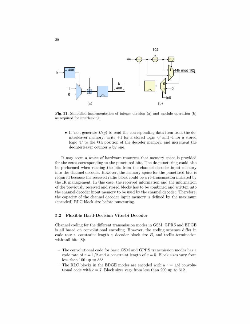
(20)with k = 0..1223, such that each encoded bit of a radio block that was notpunctured is interleaved to the address Π(k). Obtaining the de-interleaved ad-dress Π−1(k) for a specific bit position k is even more complex and difficult torealize. However, when generating the interleaved addresses in ascending order,i.e., k = 0, 1, 2, .., complex modulo and division operations can be replaced bysimple add-compare-select stages and counters (an example for such a simplifiedimplementation is illustrated in Fig. 11 for a modulo and for a divide opera-tion of (20)). Therefore, the de-interleaving can be performed most efficientlyby applying the interleaved positions (generated in ascending order) as read ad-dresses to the de-interleaver memory and writing the corresponding data itemsto the channel decoder input memory in natural order. With de-/puncturingthe situation is similar: generating the bit positions which have to be puncturedcan be implemented efficiently with counters, whereas the inverse operation ofdetermining if a specific address has been punctured is a complex task.
In order to minimize implementation complexity in our ASIC design, weapply the write addresses to the decoder input memory in natural (ascending)order and perform the de-puncturing and de-interleaving in a combined step:
– Initialization of the de-interleaver counter to q = 0.– For all k = 0, 1, 2, .. in ascending order check if the kth bit has been punctured
in the transmitter.• If ’yes’, write a zero (no a-priori information available for channel decod-
ing) to the kth position of the channel decoder input memory.
20
1
0
= 408k
k408
(a)
44
102
44k mod 102
≥0
0
init
1
0
0
1
(b)
Fig. 11. Simplified implementation of integer division (a) and modulo operation (b)as required for interleaving.
• If ’no’, generate Π(q) to read the corresponding data item from the de-interleaver memory: write +1 for a stored logic ’0’ and -1 for a storedlogic ’1’ to the kth position of the decoder memory, and increment thede-interleaver counter q by one.
It may seem a waste of hardware resources that memory space is providedfor the zeros corresponding to the punctured bits. The de-puncturing could alsobe performed when reading the bits from the channel decoder input memoryinto the channel decoder. However, the memory space for the punctured bits isrequired because the received radio block could be a re-transmission initiated bythe IR management. In this case, the received information and the informationof the previously received and stored blocks has to be combined and written intothe channel decoder input memory to be used by the channel decoder. Therefore,the capacity of the channel decoder input memory is defined by the maximum(encoded) RLC block size before puncturing.
5.2 Flexible Hard-Decision Viterbi Decoder
Channel coding for the different transmission modes in GSM, GPRS and EDGEis all based on convolutional encoding. However, the coding schemes differ incode rate r, constraint length c, decoder block size B, and trellis terminationwith tail bits [8]:
– The convolutional code for basic GSM and GPRS transmission modes has acode rate of r = 1/2 and a constraint length of c = 5. Block sizes vary fromless than 100 up to 338.
– The RLC blocks in the EDGE modes are encoded with a r = 1/3 convolu-tional code with c = 7. Block sizes vary from less than 200 up to 612.
21
– To reduce the coding overhead in the relatively short header sequences of theEDGE modes, the headers are encoded with tail-biting codes [23, 24]. Here,no tail bits indicating the initial and final state of the convolutional encoderare transmitted. Instead, only the fact that the initial and final state of thetail-biting convolutional encoder are identical can be used by the decoder tofind the most probable sequence.
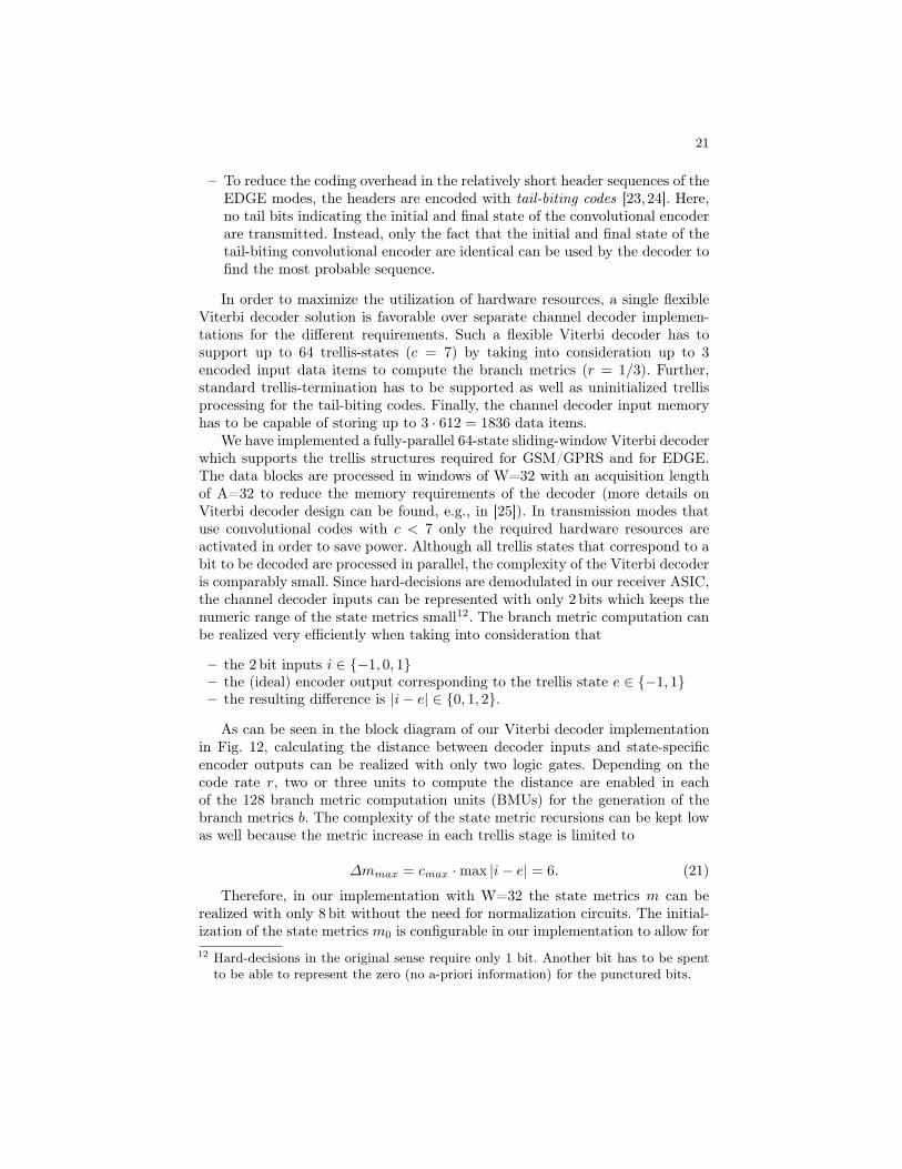
In order to maximize the utilization of hardware resources, a single flexibleViterbi decoder solution is favorable over separate channel decoder implemen-tations for the different requirements. Such a flexible Viterbi decoder has tosupport up to 64 trellis-states (c = 7) by taking into consideration up to 3encoded input data items to compute the branch metrics (r = 1/3). Further,standard trellis-termination has to be supported as well as uninitialized trellisprocessing for the tail-biting codes. Finally, the channel decoder input memoryhas to be capable of storing up to 3 · 612 = 1836 data items.
We have implemented a fully-parallel 64-state sliding-window Viterbi decoderwhich supports the trellis structures required for GSM/GPRS and for EDGE.The data blocks are processed in windows of W=32 with an acquisition lengthof A=32 to reduce the memory requirements of the decoder (more details onViterbi decoder design can be found, e.g., in [25]). In transmission modes thatuse convolutional codes with c < 7 only the required hardware resources areactivated in order to save power. Although all trellis states that correspond to abit to be decoded are processed in parallel, the complexity of the Viterbi decoderis comparably small. Since hard-decisions are demodulated in our receiver ASIC,the channel decoder inputs can be represented with only 2 bits which keeps thenumeric range of the state metrics small12. The branch metric computation canbe realized very efficiently when taking into consideration that
– the 2 bit inputs i ∈ {−1, 0, 1}– the (ideal) encoder output corresponding to the trellis state e ∈ {−1, 1}– the resulting difference is |i− e| ∈ {0, 1, 2}.
As can be seen in the block diagram of our Viterbi decoder implementationin Fig. 12, calculating the distance between decoder inputs and state-specificencoder outputs can be realized with only two logic gates. Depending on thecode rate r, two or three units to compute the distance are enabled in eachof the 128 branch metric computation units (BMUs) for the generation of thebranch metrics b. The complexity of the state metric recursions can be kept lowas well because the metric increase in each trellis stage is limited to
∆mmax = cmax ·max |i− e| = 6. (21)
Therefore, in our implementation with W=32 the state metrics m can berealized with only 8 bit without the need for normalization circuits. The initial-ization of the state metrics m0 is configurable in our implementation to allow for12 Hard-decisions in the original sense require only 1 bit. Another bit has to be spent
to be able to represent the zero (no a-priori information) for the punctured bits.
22
path
memory
Convolutional encoder
polynome look-up table
|i1-e1| |i2-e2| |i3-e3|
compare-select
Σ
i’0
e
b’0
b’1
i’1
p
i i
b b
m
decisions
path
memory
BMU BMU
decoded bits in
correct order
state metric recursions
branch metric computation
traceback and output buffering
p
1 11 10 00 00 10 1
010101
1 00 00 10 10 01 0
i’1 i’0 e b’1 b’0
e from polynome LUT: -1 mapped to logic 0+1 mapped to logic 1
0..63 0..63
0..63 0..63
0..63
0..63
0..310..1
init
m0
Fig. 12. Block diagram of the flexible 64-state parallel Viterbi decoder implementedin our design.
uninitialized decoder runs in order to find the most probable start- and end-stateof the trellis in tail-biting mode. Then, these are used in a second decoder runto decode the (header) bit sequence (details on decoding tail-biting codes canbe found, e.g., in [26,27]).
The trace-back provides the decoded bits in windows of W=32 according tothe decisions stored in the path memory in inverse order, such that an outputbuffer for 32 bits is necessary to bring them into natural order. Our channeldecoder implementation requires about 150 cycles to decode the header and 4000cycles to decode the two RLC blocks in the fastest EDGE transmission modeMCS-9. With a target clock frequency of 40MHz the decoder latency translates
23
to only about 100µs, which allows to compensate for potential delays betweenheader and data block decoding13.
5.3 Discussion: Hard-Decision vs. Soft-Decision Receiver Back-End
When designing a wireless receiver many decisions have to be taken whereperformance trades against complexity and cost. Often a specific performancegoal (e.g., BER under specific conditions) can be met with different combina-tions of devices, algorithms and architectures. E.g., choosing a radio-frequencyIC with a comparably high noise-figure could be (at least partially) compensatedfor in the digital baseband receiver by implementing the best-performing chan-nel equalizer and decoder algorithms. To find the optimum implementation for agiven application under specific constraints it is crucial to know the performanceas well as the complexity increase of the different design options.
Using demodulated soft-decision values can improve the BER after channeldecoding by 2-3 dB in terms of SNR (e.g., [28]). However, the generation of soft-decision outputs with a Viterbi equalizer is complex and significantly increasesthe required memory capacity. For each incoming branch to each trellis statethe corresponding sum of the branch and state metric has to be stored. Hence,assuming an 8-state DFSE with a 58-stage trellis using 12 bit state metrics and8 incoming branches (8PSK) to each trellis state (as implemented in our ASIC,cf., Section 4.3) the soft-output DFSE would require an additional 44.5 kb ofmemory capacity. To generate reliable soft-decisions several paths have to betraced back for each trellis stage [29] which is difficult to realize in hardware andwhich significantly increases the required number of memory accesses duringback-tracing, leading to higher power consumption.
Storing soft-decisions instead of hard-decisions in the de-interleaver and chan-nel decoder input memory requires a higher storage capacity, and processingsoft-inputs in the Viterbi decoder increases the complexity of the BMU andstate metric recursion units.
The implemented digital baseband receiver ASIC with hard-decision DFSEoutputs contains RAMs to store 20 kb. With typical soft-decisions of 5 bit in-stead, 76 kb memory would be required which translates to an increase of thecore size by a factor of more than 2, and to a chip where more than 2/3 of thesilicon area are occupied only by memory.
Even more dramatic are the savings achieved by using hard-decision equal-izer outputs when thinking of the memory required for the storage of previouslyreceived and not correctly decoded radio blocks for IR. According to the specifi-cations, a multi-slot class 12 user equipment 14 has to store up to 24 radio blocks
13 The header information has to be extracted and processed first (typically by higherlayers) to obtain the coding scheme, puncturing pattern and RLC block identifier.When a re-transmission has occurred the previously received data block will berestored from an IR memory to combine it with the received data block in thechannel decoder input memory.
14 Such a MS is capable of receiving on 4 time slots per frame.
24
5 10 15 20 25 30
1%
10%
30%
100%
SNR
BLER
MCS1
MCS2
MCS3
MCS4
MCS5
MCS6
MCS7
MCS8
MCS9
}GMSK8PSK}
Fig. 13. Receiver block error-rates in various modulation and coding schemes (MCS)of EDGE for the specified Hilly Terrain (HT) test channel with a vehicle speed of100 km/h.
with the modulation and coding scheme MCS-9, which translates to about 150 kbusing 5 bit soft-values. With hard-decisions only the puncturing pattern and theactual bits have to be stored, which saves as much as 120 kb memory.
6 Implementation Results
Functional tests and power measurements of fabricated chips (see Fig. 14) havebeen performed on a digital tester. The fixed-point simulation model of theimplemented design has been verified and used to generate the block error-rates (BLERs) of the receiver as shown in Fig. 13 for the various modulationand coding schemes (MCS) of EDGE with the specified Hilly Terrain (HT) testchannel with a vehicle speed of 100 km/h. It should be noted that the standardrequires MCS1-6 to achieve a BLER of 10% and MCS7 to achieve a BLER of30% at a certain receive power level. For MCS8-9 there are no specificationsfor these propagation conditions. Assuming the noise-figure of a state-of-the-
25
art RF transceiver IC15 these BLERs can be achieved at the specified powerlevels. Other key characteristics are summarized in Table 1. The ASIC occupies1.0mm2 in 0.13µmCMOS, comprising 97 kGE and 20 kb of memory. A measuredmaximum clock frequency of 172MHz allows the supply voltage to be loweredto 0.6V when operating at the target frequency of 40MHz. During continuousburst reception the average power consumption is as low as 5.2mW in the fastestEDGE transmission mode MCS9, and only 1.3mW when lowering the supplyvoltage to 0.6V.
Fig. 14. EDGE receiver ASIC micrograph with highlighted units.
15 E.g., IRIS305 from ACP AG, a single-chip RF transceiver supporting both TD-SCDMA/HSPA (3G) and GSM/GPRS/EDGE (2.5G) standards.
26
Technology 0.13 µm CMOS
Supply Voltage VDD 1.2V-0.6V
Core Size 1.0mm2
Gate Count 97 kGE
Total Memory 20.3 kb
Max. System Clock Frequency 172MHz
Leakage current @ VDD=1.2V (0.6V) 0.49mA (0.15mA)
Average power measured during continuous burst
reception @ target frequency f=40MHz, VDD=1.2V (0.6V)
GSM CS1 (GMSK) 2.4mW (0.6mW)
EDGE MCS9 (8PSK) 5.2mW (1.3mW)
Table 1. Key characteristics of the receiver ASIC implementation.
7 Conclusion
EDGE enables 2G data services all over the world with data rates suitable formany cellular applications. The introduction of 8PSK modulation improves thebandwidth utilization, but significantly increases equalizer complexity. Latest65 nm signal processors provide the computational power required to performthe digital baseband signal processing for EDGE. However, power and siliconarea of such implementations exceed what is desirable for a low-power, low-cost2.5G solution required in modern cellular phones.
In this work a combined architecture for GSM/GPRS/EDGE has been pre-sented. We have shown how the digital baseband can be mapped efficiently todedicated hardware by using suitable algorithms and architectures to share hard-ware resources with little overhead. A certain amount of flexibility can supportthe specified transmission modes with different modulation and coding schemes.Our approach to reduce complexity in the most crucial block, the channel equal-izer, is to maximize the effort in the pre-processing FIR filtering, in order to beable to reduce DFSE complexity. Using hard-decisions at the equalizer outputis the key to curtail memory requirements in the back-end of a digital basebandreceiver for EDGE.
With 1.0mm2 and only 1.3mW average power consumption our ASIC im-plementation shows that cost-effective multi-mode digital baseband receiver ac-celerators for GSM/EDGE can be realized at ultra low-power.
27
Acknowledgments
The authors would like to thank Andreas Burg, Andreas Bubenhofer, JohannesWidmer, Stefan Zwicky, Harald Kröll, and Christoph Roth for their support.This project was funded by CTI (No. 11370.1), Switzerland in collaborationwith Advanced Circuit Pursuit AG.
References
1. “GSM Association, Market Data, www.gsmworld.com, August 2009.”2. M. Eyuboglu and S. Qureshi, “Reduced-state sequence estimation with set parti-
tioning and decision feedback,” IEEE Transactions on Communications, vol. 36,pp. 13–20, Jan. 1988.
3. A. Duel-Hallen and C. Heegard, “Delayed decision-feedback sequence estimation,”IEEE Transactions on Communications, vol. 37, pp. 428–436, May 1989.
4. J. Olivier et al., “Efficient equalization and symbol detection for 8-PSK EDGEcellular system,” IEEE Transactions on Vehicular Technology, vol. 52, pp. 525–529, May 2003.
5. W. Gerstacker and R. Schober, “Equalization concepts for EDGE,” IEEE Trans-actions on Wireless Communications, vol. 1, pp. 190–199, Jan. 2002.
6. L. Szczecinski and I. Soto, “Is turbo equalization useful in EDGE systems?,” Ve-hicular Technology Conference, vol. 1, pp. 80–84, May 2002.
7. C. Laot, R. Le Bidan, and D. Leroux, “Low-complexity MMSE turbo equalization:a possible solution for EDGE,” IEEE Transactions on Wireless Communications,vol. 4, pp. 965–974, May 2005.
8. 3GPP Organizational Partners, Sophia Antipolis Valbonne, France, 3rd Genera-tion Partnership Project; Technical Specification Group GSM/EDGE Radio AccessNetwork; Channel Coding, June 2009.
9. 3GPP Organizational Partners, Sophia Antipolis Valbonne, France, 3rd Genera-tion Partnership Project; Technical Specification Group GSM/EDGE Radio AccessNetwork; Modulation, Dec. 2008.
10. 3GPP Organizational Partners, Sophia Antipolis Valbonne, France, 3rd Genera-tion Partnership Project; Technical Specification Group GSM/EDGE Radio AccessNetwork; Radio transmission and reception, June 2009.
11. J. Proakis, Digital Communications, 4th Edition. New York, NY, USA: McGraw-Hill Higher Education, 2001.
12. M. Schmidt and G. Fettweis, “Fractionally-spaced prefiltering for reduced stateequalization,” in Global Telecommunications Conference, 1999. GLOBECOM ’99,vol. 5, pp. 2291 – 2295, 1999.
13. J. O. III Smith, Introduction to Digital Filters: with Audio Applications. W3KPublishing, 2004.
14. W. Gerstacker et al., “On prefilter computation for reduced-state equalization,”IEEE Transactions on Wireless Communications, vol. 1, Oct. 2002.
15. A. V. Oppenheim and R. W. Schafer, Digital Signal Processing, 1st edition. En-glewood Cliffs, NJ: Prentice-Hall, Inc., 1989.
16. T. Detert, “Prefiltered low complexity tree detection for frequency selective fad-ing channels,” in Vehicular Technology Conference, 2007. VTC2007-Spring. IEEE65th, pp. 2364 –2368, Apr. 2007.
28
17. W. C. Chu, Speech coding algorithms : foundation and evolution of standardizedcoders. Hoboken, NJ: John Wiley & Sons, Inc., 2003.
18. J. Makhoul, “Linear prediction: A tutorial review,” in Proceedings of the IEEE,pp. 561 – 580, Apr. 1975.
19. G. Golub and C. Van Loan, Matrix computations. Johns Hopkins University Press,1996.
20. C. Benkeser, Power Efficiency and the Mapping of Communication Algorithms intoVLSI. PhD thesis, ETH Zürich, Switzerland, Series in Microelectronics, vol. 209,Hartung-Gorre Verlag Konstanz, 2010.
21. E. Seurre, P. Savelli, and P.-J. Pietri, EDGE for Mobile Internet. Norwood, MA:Artech House, 2003.
22. A. Viterbi, “Error bounds for convolutional codes and an asymptotically optimumdecoding algorithm,” IEEE Transactions on Information Theory, vol. 13, pp. 260–269, Apr. 1967.
23. H. Ma and J. Wolf, “On tail biting convolutional codes,” Communications, IEEETransactions on, vol. 34, pp. 104 – 111, feb 1986.
24. E. Biglieri, Coding for wireless channels. New York, NY: Springer, 2005.25. T. Truong, M.-T. Shih, I. Reed, and E. Satorius, “A VLSI design for a trace-back
Viterbi decoder,” Communications, IEEE Transactions on, vol. 40, pp. 616 –624,mar 1992.
26. R. Cox and C. Sundberg, “An efficient adaptive circular Viterbi algorithm fordecoding generalized tailbiting convolutional codes,” Vehicular Technology, IEEETransactions on, vol. 43, pp. 57 –68, feb 1994.
27. J. Anderson and S. Hladik, “An optimal circular Viterbi decoder for the boundeddistance criterion,” Communications, IEEE Transactions on, vol. 50, pp. 1736 –1742, nov 2002.
28. G. Clark and J. Cain, Error-correction coding for digital communications. NewYork; London: Plenum Press, 1981.
29. J. Hagenauer and P. Hoeher, “A Viterbi algorithm with soft-decision outputs andits applications,” in Global Telecommunications Conference, 1989, and Exhibition.Communications Technology for the 1990s and Beyond. GLOBECOM ’89., IEEE,pp. 1680 –1686 vol.3, nov 1989.