HAL Id: tel-01278998 https://tel.archives-ouvertes.fr/tel-01278998 Submitted on 25 Feb 2016 HAL is a multi-disciplinary open access archive for the deposit and dissemination of sci- entific research documents, whether they are pub- lished or not. The documents may come from teaching and research institutions in France or abroad, or from public or private research centers. L’archive ouverte pluridisciplinaire HAL, est destinée au dépôt et à la diffusion de documents scientifiques de niveau recherche, publiés ou non, émanant des établissements d’enseignement et de recherche français ou étrangers, des laboratoires publics ou privés. A variability study of PCM and OxRAM technologies for use as synapses in neuromorphic systems Daniele Garbin To cite this version: Daniele Garbin. A variability study of PCM and OxRAM technologies for use as synapses in neu- romorphic systems. Micro and nanotechnologies/Microelectronics. Université Grenoble Alpes, 2015. English. NNT : 2015GREAT133. tel-01278998
Transcript
HAL Id: tel-01278998https://tel.archives-ouvertes.fr/tel-01278998
Submitted on 25 Feb 2016
HAL is a multi-disciplinary open accessarchive for the deposit and dissemination of sci-entific research documents, whether they are pub-lished or not. The documents may come fromteaching and research institutions in France orabroad, or from public or private research centers.
L’archive ouverte pluridisciplinaire HAL, estdestinée au dépôt et à la diffusion de documentsscientifiques de niveau recherche, publiés ou non,émanant des établissements d’enseignement et derecherche français ou étrangers, des laboratoirespublics ou privés.
A variability study of PCM and OxRAM technologiesfor use as synapses in neuromorphic systems
Daniele Garbin
To cite this version:Daniele Garbin. A variability study of PCM and OxRAM technologies for use as synapses in neu-romorphic systems. Micro and nanotechnologies/Microelectronics. Université Grenoble Alpes, 2015.English. NNT : 2015GREAT133. tel-01278998
DOCTEUR DE L’UNIVERSITÉ GRENOBLE ALPES Spécialité : Nanoélectronique et nanotechnologies
Arrêté ministériel : 7 août 2006
Présentée par
Daniele GARBIN Thèse dirigée par Prof. Gérard GHIBAUDO et codirigée par Dr. Barbara DE SALVO préparée au sein du CEA-LETI dans l'École Doctorale d’Électronique, Électrotechnique, Automatique et Traitement du Signal Étude de la variabilité des technologies PCM et OxRAM pour leur utilisation en tant que synapses dans les systèmes neuromorphiques Thèse soutenue publiquement le 15 décembre 2015, devant le jury composé de :
M Daniele IELMINI Prof., Politecnico di Milano, Italie, Rapporteur
M Giacomo INDIVERI Prof., Swiss Federal Institute of Technology in Zurich, Suisse, Rapporteur
M Ian O’CONNOR Prof., Ecole centrale de Lyon, Président
Mme Elisa VIANELLO Dr. Ing., CEA-Leti Grenoble, Co-encadrant de thèse
M Quentin RAFHAY MCF, Université Grenoble Alpes (IMEP-LAHC), Co-encadrant de thèse
M Gérard GHIBAUDO DR, CNRS Université Grenoble Alpes (IMEP-LAHC), Directeur de thèse
Mme Barbara DE SALVO HDR, Dr. Ing. CEA-Leti Grenoble, Co-directeur de thèse, Invité
M Olivier BICHLER Dr. Ing. CEA-List Gif-sur-Yvette, France, Invité
Abstract
Title: A variability study of PCM and OxRAM technologies for use as synapses inneuromorphic systems.
The human brain is made of a large number of interconnected networks which arecomposed of neurons and synapses. With a low power consumption of only few Watts,the human brain is able to perform computational tasks that are out of reach fortoday’s computers, which are based on the Von Neumann architecture. Neuromorphichardware design, taking inspiration from the human brain, aims to implement thenext generation of non-Von Neumann computing systems. In this thesis, emergingnon-volatile memory devices, speciőcally Phase-Change Memory (PCM) and Oxide-based resistive memory (OxRAM) devices, are studied as artiőcial synapses for usein neuromorphic systems. The use of PCM devices as binary probabilistic synapsesis proposed for complex visual pattern extraction applications. The impact of thePCM programming conditions on the system-level power consumption is evaluated.A programming strategy is proposed to avoid the PCM resistance drift. It is shownthat, using scaled devices, it is possible to reduce the synaptic power consumption.The OxRAM resistance variability is evaluated experimentally through electricalcharacterization, gathering statistics on both single memory cells and at array level.A model that allows to reproduce OxRAM variability from low to high resistancestate is developed. An OxRAM-based convolutional neural network architectureis then proposed on the basis of this experimental work. By implementing thecomputation of convolution directly in memory, the Von Neumann performancebottleneck is avoided. The robustness of the neuromorphic system to OxRAMvariability is demonstrated for complex visual pattern recognition tasks such ashandwritten characters and traic signs recognition.
i
Résumé
Titre : Étude de la variabilité des technologies PCM et OxRAM pour leur utilisationen tant que synapses dans les systèmes neuromorphiques.
Le cerveau humain est composé d’un grand nombre de réseaux interconnectés,dont les neurones et les synapses en sont les briques constitutives. Caractérisé par unefaible consommation de puissance, de quelques Watts seulement, le cerveau humainest capable d’accomplir des tâches qui sont inaccessibles aux systèmes de calculactuels, basés sur une architecture de type Von Neumann. La conception de systèmesneuromorphiques vise à réaliser une nouvelle génération de systèmes de calcul qui nesoit pas de type Von Neumann. L’utilisation de mémoires non-volatile innovantesen tant que synapses artiőcielles, pour application aux systèmes neuromorphiques,est donc étudiée dans cette thèse. Deux types de technologies de mémoires sontexaminés : les mémoires à changement de phase (Phase-Change Memory, PCM)et les mémoires résistives à base d’oxyde (Oxide-based resistive Random AccessMemory, OxRAM). L’utilisation des dispositifs PCM en tant que synapses de typebinaire et probabiliste est étudiée pour l’extraction de motifs visuels complexes,en évaluant l’impact des conditions de programmation sur la consommation depuissance au niveau système. Une nouvelle stratégie de programmation, qui permetde réduire l’impact de la dérive de la résistance des dispositifs PCM (dit ń drift ż)est ensuite proposée. Il est démontré qu’en utilisant des dispositifs de tailles réduites,il est possible de diminuer la consommation énergétique du système. La variabilitédes dispositifs OxRAM est ensuite évaluée expérimentalement par caractérisationélectrique, en utilisant des méthodes statistiques, à la fois sur des dispositifs isoléset dans une matrice mémoire complète. Un modèle qui permets de reproduire lavariabilité depuis le niveau faiblement résistif jusqu’au niveau hautement résistif estainsi développé. Une architecture de réseau de neurones de type convolutionnel estensuite proposée sur la base de ces travaux éxperimentaux. La tolérance du systèmeneuromorphique à la variabilité des OxRAM est enőn démontrée pour des tâches dereconnaissance de motifs visuels complexes, comme des caractères manuscrits ou despanneaux de signalisations routières.
ii
Contents
Acknowledgments 1
Introduction 2
1 Emerging Non Volatile Memories and Neuromorphic Systems 4
This PhD thesis was prepared at the Université Grenoble Alpes, CEA LETI andIMEP-LAHC. First of all, I would like to thank my PhD thesis directors Prof. GérardGhibaudo and Dr. Barbara De Salvo, for their precious guidance and wisdom. Then,I would like to thank my advisors Dr. Elisa Vianello and Dr. Quentin Rafhay forsupporting me and helping me improve during these three years. I thank all the LCMteam: Luca Perniola, Eric Jalaguier, Gabriele Navarro, Véronique Sousa, GabrielMolas, Alain Persico, Christelle Charpin, Sophie Bernasconi, Carine Jahan, RémiCoquand, Etienne Nowak, Laurent Grenouillet, Cathérine Carabasse, Jean-FrançoisNodin, Guillaume Bourgeois, Jérôme Lozat and Khalil El Hajjam. I would like tothank Dr. Olivier Joubert and the LabEx Minos for supporting my PhD thesis underGrant ANR-10-LABX-55-01.
I am deeply grateful to Dr. Olivier Bichler for our nice and fruitful collaboration.I would also like to thank Dr. Christian Gamrat for welcoming me during the timethat I spent in CEA LIST. I thank Alain Lopez, Jacques Cluzel, Denis Blachier,Carlo Cagli, Giovanni Romano, Olga Cueto, and all the people from LCTE and LICLlaboratories for their support. I thank our collaborators from STMicroelectronics forproviding most of the samples that I tested during this research.
I thank all the PhD students, interns and postdocs who shared with me cofeebreaks, lunches, trips and happy moments during the last three years: Marinela,Thanasis, Manan, Boubacar, Quentin, Thomas, Gabriele, Giorgio, Thérèse, Jérémy,Florian, Yann, Sebastien, Amine, Julien, Issam, Sarra, Heimanu, Rémi, Luca, Niccolò,Thilo, Julia, Mourad, Mouhamad, Giuseppe, Cécile, Adam, Daeseok, Luc, Martin,Davide, Marco, Aurore, Fabien, Loïc, Romain, Vincent, Jose, Mathilde, Corentin,Anouar, Mathias, Patricia, Alexandre, Anthony, Louise, Jessy and all those peoplethat i may have forgotten in this list. I would also like to thank Sabine, Brigitte,Sylvaine and Malou for their help during these three years.
I am grateful to Prof. Ian O’Connor, Prof. Daniele Ielmini and Prof. GiacomoIndiveri for accepting to review this thesis and attending my PhD defense.
Last but not least, I thank my family for their support and for always being therefor me.
1
Introduction
The human brain is made of a large number of interconnected networks which arecomposed of neurons and synapses. With a low power consumption of only fewWatts, the human brain is able to perform computational tasks that are out ofreach for today’s computers, currently are based on the Von Neumann architecture.Neuromorphic hardware design, taking inspiration from the human brain, aims toimplement the next generation of non-Von Neumann computing systems. Neuromor-phic systems are designed to perform, in a power eicient way, those tasks at whichthe human brain is excellent, as for example the recognition of complex visual andauditory patterns.
Emerging Non-Volatile Memory (NVM) devices have been studied in the recentyears as possible solutions to implement artiőcial synapses in neuromorphic hardwaresystems. In this work, emerging NVM devices, in particular Phase-Change Memory(PCM) and Oxide-based resistive memory (OxRAM) devices, are studied havingin mind the central role that they will play in future memory and computingarchitectures. We investigate the use of these devices for the implementation ofartiőcial synapses, with a special focus on device variability and its impact on theperformance of neuromorphic computing systems.
Manuscript outline
In Chapter 1, we introduce the context and motivation behind the research conductedduring the preparation of this PhD. Given the interdisciplinarity involved in thisproject, this chapter describes in depth the basics concepts that are needed tocontextualize this research, in the framework of both conventional memory andneuromorphic computing architectures.
In Chapter 2, we focus on PCM technology, one of the most mature among theemerging non-volatile memory technologies. PCM devices ofer the possibility ofmultilevel programming by gradually changing the size of the crystalline portionof the active phase-change material. We analyze the drawbacks related to the useof the multilevel PCM synapse approach. Therefore, driven by the motivation toovercome the limitations associated to the multilevel programming, we explore bysimulations the use of PCM synapses operated in binary mode, where only two
2
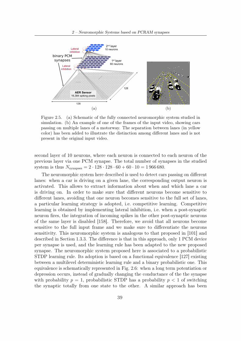
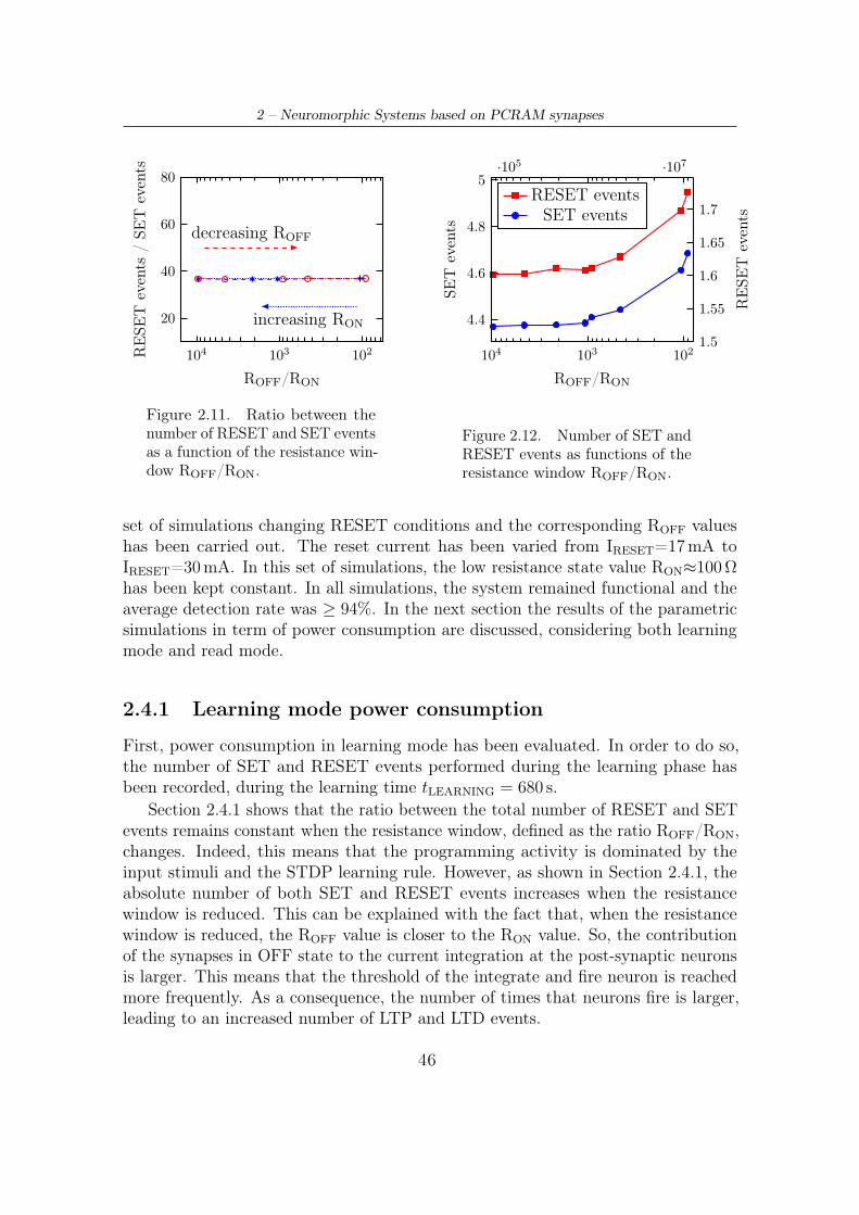
resistance states are exploited. The use of the proposed binary PCM synapse isstudied in a neuromorphic system designed for complex visual pattern extraction.
In Chapter 3, we investigate the binary operation of OxRAM devices. Sincevariability is the main drawback of OxRAM technology, we carry out an extensive workof electrical characterization on single bitcells and on 16 kb memory array, in orderto understand the source of variability. Starting from the electrical characterizationresults, we develop a simpliőed trap-assisted tunneling model to reproduce theOxRAM variability from low (LRS) to high resistance state (HRS), highlighting thecontinuity of the mechanisms involved in the variability. We carry out this analysiswith a dual goal. On one hand, the developed model provides an insight on the sourceof variability in OxRAM, suggesting technology guidelines for the improvement ofreliability. On the other hand, the computational eiciency of the developed modelallows to simulate large memory arrays and take into account the synaptic variabilitycorresponding to a wide range of programming conditions in neuromorphic systemsimulations.
In Chapter 4 we propose an OxRAM-based synapse design that combines togetherthe advantages of multilevel and binary approaches. Using such synapses, we proposea hardware implementation of a convolutional neural network (CNN) for complexvisual applications such as handwritten digits and traic signs recognition. Weinvestigate the tolerance of the proposed network to both temporal and spatialsynaptic variability.
In Chapter 5 we provide a general conclusion of the research carried out for thisthesis. Finally, we provide a perspective on the future work that needs to be donefor the further progress of the research on neuromorphic hardware.
3
Chapter 1
Emerging Non Volatile Memories
and Neuromorphic Systems
In this chapter, we introduce the context and motivation behind the research con-ducted during the preparation of this PhD. On one side, emerging Non-VolatileMemory (NVM) devices are studied having in mind the central role that they will playin the memory architectures of the future. On the other side, a novel application ofNVM devices, which has gained a large interest over the last few years, is investigated:the implementation of artiőcial synapses in brain-inspired computing architectures.Given the interdisciplinarity involved in this project, this chapter describes in depththe basics concepts that are needed to contextualize this research, in the frameworkof both conventional memory and neuromorphic computing architectures.
1.1 The semiconductor memory market
The design of today’s computing systems is based on the Von Neumann architec-ture [1]. In this architecture, a marked distinction exists between the role of theCentral Processing Unit (CPU) and the Memory Unit (MU). The CPU is in charge ofperforming the arithmetic operations, logic functions, control tasks and input/outputoperations that are speciőed by a set of instructions, i.e. a computer program, whichis stored in the MU. The MU contains both the code of the computer programs andthe data. Data comprise the information that has to be processed by the CPU andthe results of the computation [1].
The simplest architecture for organizing memory is the flat memory architecture.In this architecture, data are stored in a single, large memory unit block in the formof array. However, the memory access time and the power consumption associated tothe access to information increase with the size of the memory array. Hence, memorypower and access time dominate the total power and performance when a largestorage is required for computation [2]. In fact, a gap exists between processor and
4
1 – Emerging Non Volatile Memories and Neuromorphic Systems
Figure 1.1. The memory hierarchy in computers. Small amounts of high-performance volatile and expensive memory are close to the CPU. Large amountsof slower, non volatile and low-cost storage units are far from the CPU at thebottom of the hierarchy. Source: [4].
memory in terms of performance: computation performance is typically limited byhow fast the data in memory can be accessed, with latency and bandwidth being themain limiting factors. This gap is commonly referred to as the memory bottleneck[2].
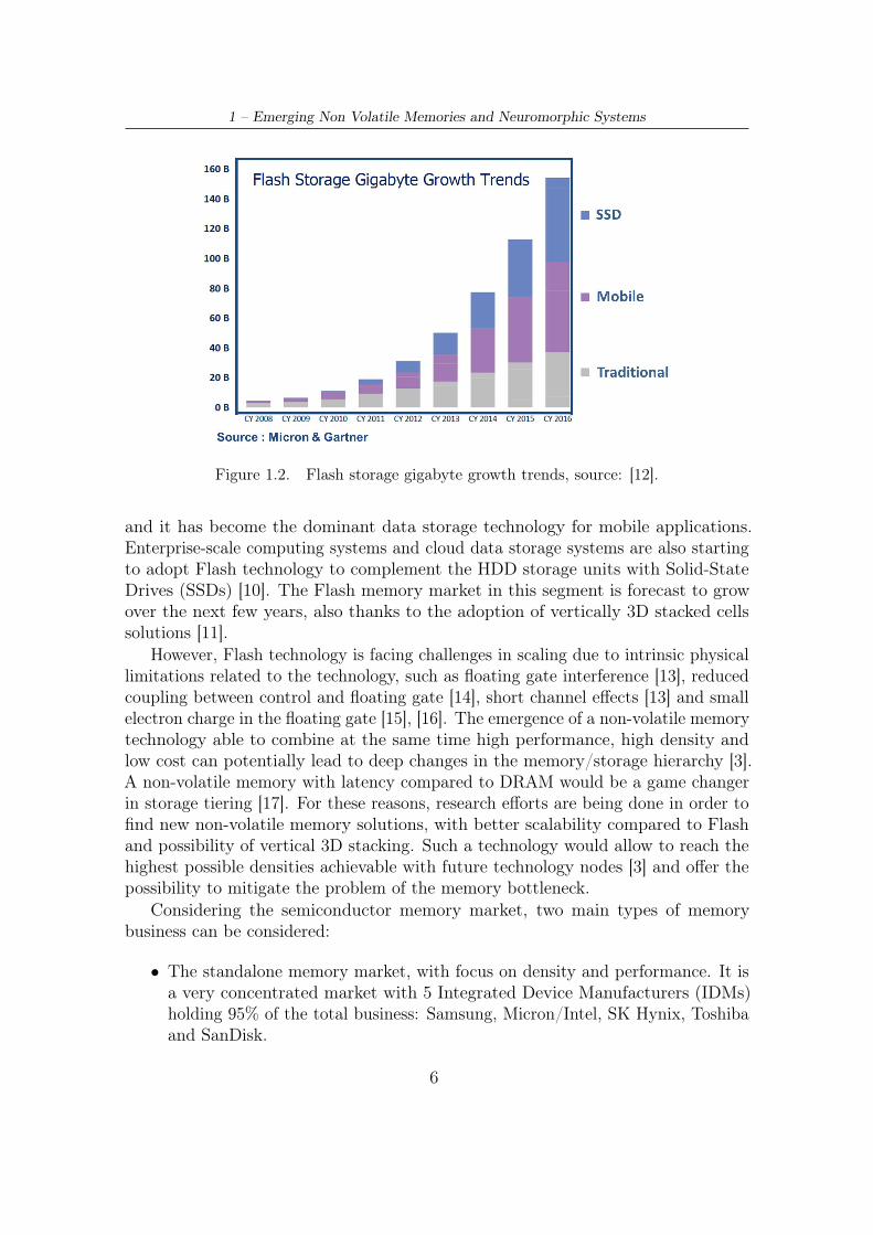
In more advanced memory architectures, memory is not flat. It is structuredas a hierarchy of volatile and non-volatile memory devices, in order to achieve anoptimal trade-of between cost and performance. The goal of this memory hierarchy,shown in Figure 1.1, is to mitigate the problem of the memory bottleneck, bridgingthe performance gap between the fast CPU and the slower memory and storagetechnologies, keeping the system costs down [3]. As illustrated in Fig. 1.1, at thetop of the hierarchy, close to the CPU unit, is the memory that is accessed mostfrequently. Static Random Access Memory (SRAM) is the technology of choicebecause it allows the fastest operation speed. However, due to the large silicon arearequired, it is also the most expensive technology [4]. The technology adopted forthe main memory is typically the Dynamic Random Access Memory (DRAM), whichoften resides in a diferent chip than the CPU because the technology process isdiferent. For over 30 years, SRAM [5] and DRAM [5] technology have dominatedthe memory market [6]. Both SRAM and DRAM, however, are volatile memories,i.e. the information stored in memory is lost when the device is turned of. At thebottom of the memory hierarchy, magnetic Hard Disk Drives (HDDs) have beenused for over 50 years [7] as a őrst choice for non-volatile storage solutions. Since theadvent and explosive growth of portable devices such as music players and cellularphones, however, Flash memory [8], [9] has forced its way into the information storagehierarchy, between DRAM and HDD, as non-volatile storage solution. As shownin Fig. 1.2, the growth of Flash technology has exploded over the last few years,
5
1 – Emerging Non Volatile Memories and Neuromorphic Systems
and it has become the dominant data storage technology for mobile applications.Enterprise-scale computing systems and cloud data storage systems are also startingto adopt Flash technology to complement the HDD storage units with Solid-StateDrives (SSDs) [10]. The Flash memory market in this segment is forecast to growover the next few years, also thanks to the adoption of vertically 3D stacked cellssolutions [11].
However, Flash technology is facing challenges in scaling due to intrinsic physicallimitations related to the technology, such as ŕoating gate interference [13], reducedcoupling between control and ŕoating gate [14], short channel efects [13] and smallelectron charge in the ŕoating gate [15], [16]. The emergence of a non-volatile memorytechnology able to combine at the same time high performance, high density andlow cost can potentially lead to deep changes in the memory/storage hierarchy [3].A non-volatile memory with latency compared to DRAM would be a game changerin storage tiering [17]. For these reasons, research eforts are being done in order toőnd new non-volatile memory solutions, with better scalability compared to Flashand possibility of vertical 3D stacking. Such a technology would allow to reach thehighest possible densities achievable with future technology nodes [3] and ofer thepossibility to mitigate the problem of the memory bottleneck.
Considering the semiconductor memory market, two main types of memorybusiness can be considered:
• The standalone memory market, with focus on density and performance. It isa very concentrated market with 5 Integrated Device Manufacturers (IDMs)holding 95% of the total business: Samsung, Micron/Intel, SK Hynix, Toshibaand SanDisk.
6
1 – Emerging Non Volatile Memories and Neuromorphic Systems
Other Memory (EEProm,
ROM, emerging NVM…)
2% DRAM 53%
SRAM 2%
Flash NAND 38%
Flash NOR 5%
Standalone memory business 2013 ($67B)
(a)
MPU mobile SRAM 60%
MCU NVM 27%
MCU SRAM 13%
Embedded memory business 2013 ($15B)
(b)
Figure 1.3. (a) Standalone and (b) embedded memory market in 2013. Source: [18].
• The embedded memory market, with low power consumption and high thermalstability being some of the most restricting speciőcations. There are two typesof embedded memory, depending on the level of system integration. I Systemon Chip (SoC) such microcontrollers (MCUs) for smart cards, automotive ormobile microprocessors (MPUs) for portable systems. II System in Package(SiP) where a number of integrated circuits are enclosed in a single module(package). The embedded memory market is more fragmented, with foundriesmanufacturing the bulk part of the total production [18].
As shown in Fig. 1.3a, Flash NAND technology and DRAM currently dominatethe standalone memory market, representing about 90% of overall memory sales. Alow-cost emerging memory technology with densities larger than Flash and speedcomparable to DRAM can possibly conquer a large portion of the market. After2020, emerging NVM could also replace SRAM in the MCU and MPU embeddedmemory business [18] (Fig. 1.3b).
1.2 Emerging non-volatile memory technologies
In the quest for innovative non-volatile memory solutions, diferent technologies haveemerged in research over the last 15 years [19], [20]. These technologies are free fromthe limitations of Flash, which are low endurance (i.e. a limited number of writeoperations is possible), need for high voltage supply for programming, long writetime and complex erase procedure [4]. Another limitation of Flash is the fact that itis a Front-End-Of-Line (FEOL) technology, diicult to co-integrate with sub-32 nmCMOS [16].
The main emerging non-volatile memory technologies are the following:
• Phase-Change Random Access Memory (PCRAM or PCM);
• Spin-Transfer-Torque Magnetic Random Access Memory (STT-MRAM);
7
1 – Emerging Non Volatile Memories and Neuromorphic Systems
• Conductive-Bridging Random Access Memory (CBRAM);
• metal Oxide resistive Random Access Memory (OxRAM).
These emerging memory technologies store information using physical mechanismswhich do not rely on storing charge in a capacitor or the ŕoating gate of a transistoras in the case of SRAM, DRAM and Flash. They are integrated in the Back-End-Of-Line. It is worth noticing that in literature the generic term resistive RAM (RRAMor ReRAM) is often used to generically refer to both OxRAM and CBRAM. In thenext sections, an overview of the main emerging non-volatile memory technologieswill be given, with details on some important properties and performance aspects.
1.2.1 PCRAM
Phase-Change Random Access Memory (PCRAM, or PCM) working principle isbased on the electrical properties of phase-change materials. Phase-change materials,in fact, feature a high contrast in resistivity between amorphous and crystallinephases. The amorphous phase is characterized by a high electrical resistivity, whilethe crystalline phase features low resistivity [21]. In PCRAM it is possible to switchthe material between amorphous and crystalline phase multiple times. Most ofphase-change materials are chalcogenides, which are alloys featuring at least oneelement from the VI group of the periodic table. Ge2Sb2Te5 (GST) is one of the moststudied chalcogenide phase-change materials. Other examples are GeTe, GeSeTe2,AgSbSe2 [21] and diferent variants obtained by doping [22], [23] or enrichment ofalloying elements [24], [25]. GaSb is an example of phase-change material that is nota chalcogenide [26].
In PCRAM, the phase-change material is switched between amorphous and crys-talline phase by Joule heating. Figure 1.4a shows the shape of typical current-voltagecharacteristics for crystalline and amorphous phases of phase-change materials. Crys-tallization is achieved by heating the material above its crystallization temperature(SET operation). Amorphization is achieved by melting the material in the liquidstate and rapidly quenching it into the disordered amorphous phase (RESET opera-tion). These operations are performed by electrical current pulses: high-power pulsesare required for the RESET operation, moderate power but longer duration pulsesare used for the SET operation. In order to retrieve the information, low powerpulses are used to sense the resistance of the device [21]. Figure 1.4b shows schemat-ically a mushroom-shaped PCRAM cell. The device is composed of a phase-changematerial sandwiched between a top electrode and a bottom electrode in the form ofsmall cross-section heater plug. The active region is deőned as the portion of thephase-change material that actually undergoes phase switching. It is located rightabove the heater plug, where the temperature reaches the highest value due to highcurrent density.
8
1 – Emerging Non Volatile Memories and Neuromorphic Systems
IProgram
SET
RESETRead
SET
Amorphous
Crystalline
V
p
(a)
Top electrode
Phase-changeg
material
Active region
Dielectric
material
Bottom electrode ((b)
Figure 1.4. (a) Typical current-voltage characteristics of crystalline andamorphous phases of phase-change materials. (b) Schematic cross-section of aphase-change memory cell. Source: [27].
One of the limiting factors for the adoption of PCRAM technology is the relativelyhigh RESET current [28]. However, the programming current scales down withdevice area. In ultra-scaled devices with 10 nm feature size, the RESET current isshown to decrease down to the microampere range [29]. Furthermore, material andinterface engineering can signiőcantly contribute to the reduction of the RESETcurrent [23], [30].
One of the attractive features of PCRAM is the possibility of achieving multilevel-cell (MLC) storage. This means that the device can be programmed into multi-levelresistance states, in addition to the full SET and RESET resistance levels. Thisis obtained by modulating the ratio between the crystalline and amorphous regionsize within the active region. MLC functionality is an eicient way of decreasingthe cost of memory, because it alows to store more information for a given siliconarea [31]. However, in phase change materials the amorphous intermediate resistancestates drift with time t towards higher resistance values, following a R(t) = R0(t/t0)
ν
relationship, where R0 is the resistance at initial time t0, and ν is the drift coeicient,which depends on the material and on the device morphology [32]. As a consequence,after a certain amount of time has passed after programming, it is a not trivial task todistinguish the programmed states. Only using advanced cell readout methodologieswhich are intrinsically resilient to resistance drift, a reliable 2 bits/cell storage anddata retention at high temperature can be achieved [31].
9
1 – Emerging Non Volatile Memories and Neuromorphic Systems
1.2.2 STT-RAM
In Spin-Transfer-Torque Magnetic Random Access Memory (STT-MRAM) devices,information is stored in the orientation of the magnetization of a nano-scale ferromag-netic layer. Figure 1.5a shows the schematic view of a typical STT-MRAM bit-cell.The main component of STT-MRAM is the Magnetic Tunnel Junction (MTJ), whichconsists of two magnetic layers separated by a tunneling barrier, composed of athin layer of insulating MgO. The orientation of the magnetization of the FreeLayer (FL) can be switched between two states and is used to store information.The magnetization of the Reference Layer (RL) is permanent and it serves thefunction of a stable reference for the magnetic orientation [33]. If the orientationof RL and FL are the same, the device is said to be in Parallel (P) state. If theorientation of the two layers is opposite, the device is in the Anti-Parallel (AP)state. The STT-MRAM working principle is based on two phenomena that havebeen discovered during the last two decades: the Tunnelling Magneto-Resistance(TMR) efect and the Spin-Transfer Torque (STT) efect. The TMR efect [34] is thecause of the resistivity contrast between the resistance RP in the P state and theresistance RAP in the AP state. The resistance of the device can be sensed in orderto determine which is the magnetic state of the FL, so the stored information can beretrieved. The STT efect [35]ś[37] is the efect which allows to switch the magneticorientation of the FL. When electrons ŕow through the MTJ, a torque is exertedon the magnetization of the FL. If the torque is large enough, the magnetic state ofthe FL can be switched and information is written. The write operation is achievedaccording to the direction of the current ŕow. If a positive voltage is applied to thedevice, a non-polarized current, i.e. featuring electrons with random spin orientation,is injected in the direction that goes from the RL to the FL. Electrons with a spinopposite to the RL magnetization orientation are mostly reŕected. Only the electronswith a spin having the same orientation as the RL magnetization will be transmittedby tunneling through the MTJ and will transfer their spin to the FL by STT. Theresult is that the MTJ will be in the parallel state. If a negative voltage is appliedto the device, the electrons are injected from the FL to the RL. At the interfacebetween the tunneling barrier and the RL, electrons with the same orientation as theRL will be transmitted through the MTJ. Electrons with an opposite spin will bereŕected back in the FL and switch its magnetization to the AP state. In summary,as shown in Fig. 1.5b, a positive voltage leads to AP-to-P transition. A negativevoltage leads to P-to-AP transition [38].
STT-MRAM is expected to have a very high endurance [38]. This is due to thefact that no magnetic degradation mechanism is associated to the switching of themagnetization orientation. In fact, no atoms are moved during write operations,contrary to PCRAM, CBRAM or OxRAM. However, the dielectric breakdown ofthe MgO tunnel barrier can occur if the voltage across the tunnel barrier exceedsroughly 400mV [38], [39].
10
1 – Emerging Non Volatile Memories and Neuromorphic Systems
Bit line
Bit line complement
word line
FL
RL
(a) (b)
Figure 1.5. (a) Schematic view of an STT-MRAM bit cell. The MTJ is composedof a permanent reference layer (RL), a tunnel barrier and a free layer (FL) element,with both layers magnetized perpendicular to the plane of the junction. (b) Typicalresistance-voltage characteristics, showing switching between antiparallel (AP) toparallel (P) states (positive bias) and vice versa. Source: [38].
1.2.3 CBRAM
As shown in Fig. 1.6a, the structure of Conductive-Bridging Random Access Memory(CBRAM) devices consists of a Metal-Insultator-Metal structure where the topelectrode (anode) is electrochemically active or oxidized under positive bias, andthe bottom electrode (cathode) is electrochemically inert. The insulating materialsbetween top and bottom electrode can be solid electrolytes [40] or metal oxides [41],[42]. Upon application of a positive voltage on the anode, mobile metal ions fromthe anode migrate, driven by the electric őeld, into the solid electrolyte or oxideand reduce on the inert cathode, forming a conductive őlaments (CF) composed ofelement of the top electrode (typically Cu or Ag), bridging top and bottom electrodeand bringing the device to the Low Resistance State (LRS, SET operation). Whenthe voltage is reversed, metal ions migrate back to the anode dissolving the CF andbringing the device into the High Resistance State (RESET operation) [43], [44].Figure 1.6b shows typical current voltage characteristics of CBRAM. A resistanceratio between HRS and LRS higher than 106 has been demonstrated by interfaceengineering of chalcogenide CBRAM with dual-layer electrolyte stack [45], [46]. Dueto the fact that the migration of ions is a stochastic process, the conőguration of theCF is diferent after each SET and RESET operation. This results in large resistancevariability, especially in the HRS [4].
11
1 – Emerging Non Volatile Memories and Neuromorphic Systems
Similarly to CBRAM, Oxide-based resistive RAM (OxRAM) devices are also com-posed of a simple MIM structure, where a metal oxide is sandwiched between a topand a bottom electrode as shown in Fig. 1.7a. The application of an electric őeld onthe device induces the creation and motion of oxygen vacancies VO, resulting in thepossibility of repeatedly form and destruct VO-rich conductive őlaments (CFs) inthe oxide. This corresponds to a change in the resistance of the device, which canbe switched between Low Resistance State (LRS) and High Resistance State (HRS)with SET and RESET operation, respectively. Figure 1.8 is a schematic illustrationof the switching processes. Usually for the fresh samples in the pristine resistancestate, a forming or electroforming process is needed to form a Conductive Filament(CF) in the oxide layer for the őrst time [48]. During the forming process, oxygenions drift towards the top electrode interface driven by the orientation of the electricőeld. The formation of an interface oxide layer occurs if the top electrode material isoxidizable. Otherwise, oxygen accumulates in the form of nonlattice atoms if the topelectrode material is inert. Thus, the top electrode/oxide interface behaves like anoxygen reservoir [49] for the subsequent SET/RESET operations. According to thepolarity of the voltage needed to SET and the RESET the device, OxRAM operationis classiőed into two switching modes: unipolar and bipolar. Figures 1.7b and 1.7cshow a schematic of the current-voltage characteristics for the two switching modes.
• In the unipolar switching mode (Fig. 1.7b), the SET and RESET operationsdepend only on the amplitude of the applied voltage. Thus, they can beachieved using the same programming polarity. For the RESET operation,current ŕowing through the CF causes Joule heating. The rising temperatureactivates the thermal difusion of oxygen ions, which will difuse away fromthe CF due to the concentration gradient [50], bringing the device to HRS. If
12
1 – Emerging Non Volatile Memories and Neuromorphic Systems
(a) (b) (c)
Figure 1.7. (a) Schematic of MIM structure of OxRAM devices and (b) Schematicunipolar and (c) bipolar current-voltage characteristics [48].
Figure 1.8. Schematic illustration of the working principle of OxRAM. Source: [48].
SET and RESET operations can equally occur at both positive and negativevoltage polarities, the unipolar switching mode mode is also called nonpolar.
• In bipolar switching (Fig. 1.7c), the SET and RESET operations are performedat reverse voltage polarities. The interfacial oxide layer at the top electrodemay present a signiőcant difusion barrier. In this case, thermal difusioncaused by Joule heating and concentration gradient alone is not suicient, so areverse electric őeld is needed to improve oxygen ions migration in the RESETprocess.
In order to achieve the required high temperature at the CF for the RESET
13
1 – Emerging Non Volatile Memories and Neuromorphic Systems
process, usually the unipolar devices requires a higher programming current comparedto bipolar devices. In both switching modes, the SET operation occurs by dielec-tric soft breakdown, similarly to the forming operation. SET operation, however,typically requires a lower voltage compared to the forming one [48]. In order toavoid a permanent dielectric breakdown in the forming and set process, a currentlimitation, or compliance, is needed. The compliance current is usually provided bythe semiconductor parameter analyzer in the case of devices composed of the MIMstructure only (1R devices). In the case of 1T1R device, the compliance current isobtained via the selection transistor. Self-compliance 1D1R devices, with a diode asselector device, are an attractive solution for high-density crossbar structures [51].
One of the biggest advantages of this technology is the fact that it relies onsimple structure and on materials that are widely used in semiconductor processesand current CMOS technologies. Some OxRAM material examples are HfOx , TiOx ,AlOx and TaOx .
Although the device working principle is simple, the physics that govern thefunctioning of OxRAM devices are not fully understood yet. There are controversiesabout the shape of the conductive őlament and the role that top and the bottom elec-trodes play in the switching mechanisms. The characteristics of the oxygen vacanciesin terms of thermal stability and mobility are topics of intense research [44], becausethey are related to memory performance and reliability, such as high temperaturedata retention and speed. Physical observation of real-time formation and dissolutionof CF with in-situ TEM is an active research őeld [52]ś[54], because it can giveguidelines for the improvement of the variability issue.
OxRAM variability
One of the main issues for the manufacturing and industrialization of OxRAM devicesis the reproducibility of their electrical characteristics. Large resistance variationsoccur in fact not only between devices (device-to-device variability ś d2d), but alsobetween consecutive programming cycles of the same device (cycle-to-cycle variabilityś c2c). The problem of variability has been holding OxRAM technology back fromcommercialization despite its many attractive features, because it limits the sizeof the memory array that can be implemented. In fact, as the number of devicesincreases, the distributions of the devices in LRS and HRS tend to overlap, thusmaking it impossible to sense the diference between LRS and HRS state and thusretrieve information. The resistance variability in High-Resistance State (HRS) istypically larger than the variability of the Low-Resistance State (LRS) [48]. TheHRS variability has been modeled introducing a variation on a tunneling barrierthickness [55], [56]. For LRS, it has been attributed to geometric variability of theconductive őlament (CF) shape (i.e. CF radius, constriction point...) [48], [57], [58].However, a uniőed model able to reproduce the variability from HRS to LRS [59] isstill lacking.
14
1 – Emerging Non Volatile Memories and Neuromorphic Systems
1.2.5 Comparison of NVM technologies
Table 1.1 presents a benchmark of the diferent emerging nonvolatile memory technolo-gies. Practically unlimited endurance and good speed are advantages of STT-MRAMtechnology. However the relatively low resistance ratio achievable in MTJ requiresa memory cell architecture that limits its device density. OxRAM features betterendurance and speed than PCM and CBRAM, but the problem of variability is muchworse than that of PCM and STT-MRAM. In addition, all these memories promiseto scale further than Flash and DRAM. When these emerging NVM memories wereproposed, there was hope that one of them could become the universal memory, ableto make a revolution in the memory hierarchy by meeting all speciőcations in termsof power consumption, high temperature data retention, speed, endurance, density,scalability and low cost [60]ś[62]. However, as it can be evinced from Table 1.1,researchers now generally agree that the possibility of universal memory technologyis not very realistic. Application-driven design imposes diferent speciőcations aboutmemory performance at each level of the memory hierarchy. These speciőcationsrequire trade-ofs in device characteristics that are hard to obtain with an individualmemory technology [4].
1.3 Neuromorphic systems
In addition to a drastic change in the organization of the memory hierarchy intraditional Von Neumann computing architectures, emerging non-volatile memorieshave been indicated as key players in a computation paradigm shift, beyond thetraditional Von Neumann architecture, thanks to their use as nanoscale artiőcialsynapses in neuromorphic hardware [64].
Neuromorphic hardware refers to an emerging őeld of computing systems de-sign. It takes inspiration from biological neural networks that exist in mammaliannervous system and cerebral cortex. Research in neuromorphic hardware is inter-disciplinary, requiring knowledge from computational neuroscience, neurobiology,machine learning, computer science, VLSI design and nanotechnology [65]. Unlikeconventional Von Neumann computing architectures, in neuromorphic architecturesmemory and processing are not isolated tasks. They are interleaved entities, andmemory participates in the task of processing the information [66]. Figure 1.9 showsthe spectrum of models of computing, from the traditional program-centric VonNeumann-like architectures to emerging data-centric, learned computation models.In the era of the internet of things, with 10 billion devices networked together today(50 billion by 2020) [67], a huge amount of data has to be processed. New modelsof computation that learn from data, rather than executing instruction providedby programmers, are thus fundamental. The human brain is an example providedby nature of a computing system that learns from data in an eicient way. As
15
1 – Emerging Non Volatile Memories and Neuromorphic Systems
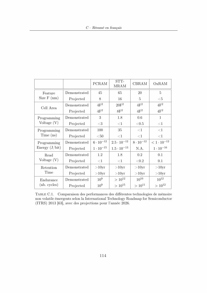
Table 1.1. Comparison of the performance of the different emerging nonvolatilememory technologies according to the 2013 International Technology Roadmap forSemiconductor (ITRS) [63], with projections for year 2026.
16
1 – Emerging Non Volatile Memories and Neuromorphic Systems
Figure 1.9. Taxonomy for traditional and emerging models ofcomputation. Source: [63].
Figure 1.10. Comparison between power consumption of extremely scaled IBMWatson supercomputer and the human brain [68].
shown in Fig. 1.10, even with extreme scaling, power consumption associated tothe Von Neumann computing architecture is orders of magnitude larger than thepower required by the human brain. The invention of new architectures is thusrequired in order to face this challenge, bridging the gap of eiciency that existsbetween conventional computing architectures and the human brain. In the questfor more eicient computation, neuromorphic hardware has been proposed as a newgeneration of computing systems, with a complementary role with respect to VonNeumann machines (Fig. 1.11).
17
1 – Emerging Non Volatile Memories and Neuromorphic Systems
Historically, the interest on neuromorphic computing systems originated in the1940s, with the presentation of the computational model for neural networks developedby McCulloch and Pitts [69]. In the late 1940s Hebb made the hypothesis thatbrain plasticity is at the basis of the human learning mechanism [70]. Researchersstarted applying these concepts to computational models in 1948 with Turing’sB-type machines [71]. In 1957, Rosenblatt developed the perceptron algorithmfor image recognition [72], implemented in hardware as the “Mark I Perceptronžor the őrst neuromorphic machine. Over the next years, the őeld was relativelystagnant because of the limitations of computational machines that processed neuralnetworks [73]. The emergence of greater computational eiciency, together withadvances with the backpropagation algorithm [74], revived the research activityin neuromorphic computing. During the 1980s, parallel distributed processingsystems started to be adopted to simulate large-scale neural networks [75]. Meadintroduced VLSI design concepts for the design of bio-inspired systems [76], with thedesign of the őrst silicon artiőcial retina and neuro-inspired learning chips on silicon.Neurocomputers, i.e. dedicated hardware implementations of processors specializedfor neural computations, emerged in the period from 1980s to early 1990s. The ZISC(Zero Instruction Set Computing) processor [77] was proposed by IBM. The ETANN(Electrically Trainable Artiőcial Neural Network) chip, featuring 10240 ŕoating-gatesynapses was presented by Intel [78]. Other examples of neurocomputers from thatperiod are L-Neuro by Philips, ANNA by AT& T, SYNAPSE 1 by Siemens [79], and
18
1 – Emerging Non Volatile Memories and Neuromorphic Systems
MIND-1024 by CEA [80]. Research advancements in neuroscience during the 1990s,particularly the interest in synaptic plasticity [81] and unsupervised learning ruleslike spike timing dependent plasticity (STDP) [82] represented a turning point inthe őeld [83]. The progress in the őeld of emerging non-volatile resistive memorytechnologies brought new life to research in neuromorphic hardware in the 2000s.
In the next section, we will brieŕy discuss the characteristics of biological neuralnetworks, composed of neurons and synapse. This is useful to understand whichcharacteristics have to be emulated in order to eiciently implement in hardware abio-inspired architecture.
1.3.1 Neurons and Synapses
The human brain is composed by a large number of interconnected networks, wherethe fundamental building blocks are neurons and synapses. It is estimated that in thehuman brain there are about 1011 neurons, and 1015 synapses [84]. Neural networksperform diferent intelligent functions inside the brain such as perception of stimuli,recognition, movement, speech.
The neuron is an electrically excitable cell that processes and transmits informa-tion through electrical signals. Neurons are connected to each other via the synapses,to form neural networks. The signals that are exchanged between neurons are calledaction potentials or spikes. As shown in Fig. 1.12, a neuron consists of three mainparts: the dendrites, the soma and the axon.
• The dendrites are the input vectors through which signals are received. Thedendrites allow the cell to receive signals from a large (>1000) number ofneighboring neurons.
• The main body of the neuron is the soma. It performs an integrate-and-őrefunction: as positive and negative signals (exciting and inhibiting, respectively)reach the soma from the dendrites, the membrane voltage of the cell is afected.
• Once the membrane voltage of the soma reaches a certain threshold value,the neuron produces a spike wich is transmitted along the axon to all otherconnected neurons dendrites.
The synapse is the connecting unit between the axon of a presynaptic neuron(pre-neuron, i.e. the neuron that is sending a spike), and a post-synaptic neuron (post-neuron, i.e. the neuron which is receiving the signal). In a synapse, the voltage spikeof the presynaptic neuron activates the voltage-controlled calcium channels presentin the presynaptic membrane. The rapid inŕux of Ca2+ into the presynapse triggersthe release of chemical substances (the neurotransmitters) in the synaptic cleft.Neurotransmitters bind to receptors located on the membrane of the postsynapticcell. The binding of the transmitters to the postsynaptic receptors causes ionic
19
1 – Emerging Non Volatile Memories and Neuromorphic Systems
Figure 1.12. Schematic view of the basic structure of a neuron cell. Inset shows azoom of the biological synapse. Source: [85].
channels to open or close, thus changing the ability of ions to ŕow into or out ofthe postsynaptic neuron. The selective permeability of these channels allow ionsto move along their electrochemical gradient, inducing a ionic current that changesthe membrane potential of the neuron (Post-Synaptic Potential, PSP). The changecan be positive (Excitatory Post-Synaptic Potential, EPSP) or negative (InhibitoryPost-Synaptic Potential, IPSP).
In the post-neuron, all ionic currents incoming from multiple synapses are summedover time and when a threshold potential is reached, an action potential (spike)is generated and sent along the axon. After that, the membrane potential of theneuron goes back to the resting threshold potential. An important characteristicsof synapses is the fact that they are plastic: their weight, i.e. the eiciency in thetransmission of signals through the synapse, changes over time according to therelative timing at which pre-synaptic and post-synaptic spikes occur. This plasticity,which is described in more detail in Section 1.3.5, is a key factor in learning andremembering.
One of the simplest artiőcial neuron model is, the Integrate and Fire (IF) neuronmodel. Figure 1.13 shows the concept of a simple IF neuron. It sums over time (inte-grates) the incoming excitatory and inhibitory signals inside the neuron integrationblock using a capacitor. More advanced designs also work with this principle [86].This integration leads to an increase in the membrane potential of the neuron Vmem.When Vmem reaches the threshold value Vth, the neuron generates an output spike.After the neuron has őred the membrane potential is restored to a resting value, by
20
1 – Emerging Non Volatile Memories and Neuromorphic Systems
Figure 1.13. Schematic image shown the basic concept of an Integrateand Fire neuron [86].
discharging the the capacitor Cmem.Many designs for the hardware implementation of artiőcial neurons on silicon,
based on standard VLSI CMOS technology, have been proposed in the literature[86]. Research activity is being carried out to optimize power and area eiciency ofneurons. Some example feature the use of non-volatile memories [87].
However, given the fact that the number of synapses is about 4 orders of magnitudelarger than the number of neurons, the real challenge is to őnd an eicient designfor the synapse, in order to be able to integrate large-scale neural networks on chip.The hardware implementation of artiőcial synapses is discussed in the next section.
1.3.2 Non-volatile memory devices as artificial synapses
Multiple solutions to implement artiőcial synapses using available VLSI devicessuch as Flash, DRAM and SRAM have been proposed in the literature [66]. Theseapproaches have the advantage of relying on already available standardized designtools and a mature fabrication process. However, some limitations exist with thisapproach [65]. Flash devices are not an ideal candidate for the implementation ofbio-inspired learning rules because they are 3-terminal devices, while real synapsesare 2-terminal. During synaptic learning individual synapses may undergo weightmodiőcation asynchronously, which is not straightforward to achieve with the ad-dressing schemes required for Flash arrays. Flash devices also require high operatingvoltages in order to program the cell. In many cases, complex pre-synaptic circuitry isrequired to implement timing dependent learning rules. This is necessary in the caseof NOR Flash, because of the diferences in the physics involved in the writing anderasing of the ŕoating gate devices, but not in the case of NAND Flash. Furthermore,Flash endurance is limited, which implies a limited amount of learning operations canoccur. Synapses based on DRAM technology are volatile and require refresh cycles
21
1 – Emerging Non Volatile Memories and Neuromorphic Systems
to retain the synaptic weight, since the information is stored as charge accumulatedon a capacitor. Typically the implementation of learning rules based on DRAMsynapse requires more than 10 additional transistors [88], [89]. The capacitor elementitself is also area-consuming. The SRAM based synapses are afected even worse bythe problem of large area consumption and are also volatile. When the network isturned of, the synaptic weights stored in SRAM are lost, so they need to be storedto a nonvolatile memory unit during or after the learning, which leads to additionalpower and area consumption. The limitations of available VLSI technologies for theimplementation of artiőcial synapses provided the motivation for research in synapticemulation using emerging non-volatile memory technologies. Recent research innanoscale devices and materials has demonstrated the possibility of emulating thebehavior of real synapses in artiőcial neural networks, and in particular to reproducetheir plasticity and non-volatility characteristics [66], [90]ś[104]. The basic ideabehind this approach is to emulate the behavior of the synapse, which is a communi-cation channel featuring variable eiciency, as a tunable resistor, implemented witha non-volatile memory (NVM) device. Some advantages of using emerging NVMs asartiőcial synapses are low-cost, full CMOS compatibility, high density, low-powerconsumption, high endurance, high temperature retention [28], [48]. NVM devices are2-terminal, as in the case of real synapses, and ofer the possibility of 3D integration.
Two main device categories can be identiőed for the implementation of artiőcialsynapses: multilevel and binary devices.
Multilevel
In the multilevel (or analog) approach, the possibility of programming individualNVMs at multiple resistance levels is exploited. Some examples feature the use ofOxRAM and CBRAM devices, where multilevel resistance levels are obtained bytuning compliance current during SET operation, or modulating the applied voltage[96]. However, this implementation is not ideal from a practical perspective. Itrequires the adoption of complicated neuron spike shapes [90], or the generation ofspikes with increasing amplitude while keeping a history of the previous state of thesynaptic device, leading to additional overhead in the neuron circuitry.
A better candidate for the multilevel approach is PCRAM technology, whichofers the possibility of gradually increasing the conductance of the device by applyingidentical SET pulses, gradually increasing the size of the crystalline region in theactive phase-change material. However, the reset process is not gradual but abrupt.
This led to the proposition of the use of two PCRAM devices per synapse, inthe 2-PCM approach proposed in [101] and recently adopted in [104]. These twodevices are connected in a complementary conőguration, where each device has anopposite contribution to the neuron’s integration. When the equivalent synapseneeds to be potentiated, the Long Term Potentiation (LTP) PCRAM device ispartially crystallized with a weak SET operation. This increases the equivalent
22
1 – Emerging Non Volatile Memories and Neuromorphic Systems
weight of the synapse. On the contrary, when the synapse must be depressed, it isthe Long Term Depression (LTD) PCM device that undergoes partial crystallization.Since the contribution of the to the neuron’s integration is negative, the equivalentweight of the synapse is decreased. With this solution, since gradual crystallizationis achieved with successive identical voltage pulses, the pulse generation schemeis greatly simpliőed. However, a systematic refresh scheme is needed to reset thedevices by retaining the weight of the synapse.
Binary
With the binary approach, only two resistance levels per NVM device are used: thelow and high resistance states (LRS and HRS). The advantage of this approachresides in the fact that it relies on programming schemes that are by all means similarto the ones used for conventional memory applications. Since only two sates of thedevice are exploited, simple SET and RESET pulses are required, optimized for speedand power consumption. It has been demonstrated that for some applications, suchas the detection of cars driving in diferent lanes of a motorway [105], a single deviceassociated to a stochastic learning rule (Section 1.3.5), is enough to achieve detectionrates comparable to the ones obtained with multilevel synapses. In Chapter 4 we willillustrate how, by connecting n devices in parallel, it is possible to obtain a multilevelconductance behavior using binary devices. Since parallel conductance sum up, theconductance of the equivalent synapses ranges from the sum of the n conductancein the HRS to the sum of all the n conductance in the LRS. The use of multipledevices is necessary for applications that are more complex than detection, such asvisual pattern recognition. This strategy comes at the cost of an increased numberof devices needed to build a synapse. The binary approach ofers the advantage of asimple programming methodology for the NVM devices, in which standard SET andRESET pulses, optimized for high endurance and low-power consumption, are usedto switch the device resistance from LRS to HRS and vice versa.
1.3.3 Fully connected neural networks
The artiőcial synapses described in Section 1.3.2 have been proposed in the literaturefor the implementation of artiőcial neural networks composed of CMOS neuronsand NVM-based synapses [66], [90]ś[104]. The network topology that has beenmostly investigated in the literature is the fully connected neural network. In thisneural network topology, neurons are organized in layers. The őrst neuron layer isconnected to the input of the network, while the last neuron layer represents theoutput of the system. The neuron layers between input and output are generallyreferred to as hidden layers. For a system designed for visual applications such aspattern detection or recognition, the raw data to be processed can be a static picture[96] or a video [101]. For auditory application the raw data is sound [105]. The raw
23
1 – Emerging Non Volatile Memories and Neuromorphic Systems
…
Fully Connected
Neural Network
topology
Layer N
Layer N+1 m neurons
n neurons m × n synapses
Figure 1.14. Fully connected neural network topology. Each neuron is connectedto every neuron of the upper layer by a large number of synapses.
data is converted into voltage spikes with a given encoding rule, and fed as an inputto the network. The conversion of the data to "spike language" understandable bythe network can be implemented with a simple algorithm, such as linear conversionfrom pixel brightness to spike frequency. It can also be obtained with bio-inspiredsensors such as artiőcial retina [106] or cochlea [107], or even electroencephalography(EEG) recording [95]. In the fully connected neural network topology, each neuronis connected to every neuron of the next layer as shown in Fig. 1.14. The spikesignals propagate through from input to output through the hidden layers of thenetwork, undergoing a transformation that is deőned by the weight of the synapses.The output neuron layer can be composed of a single or multiple neurons. A singleneuron is used if the network is used to detect a pattern in time. An example isdetecting a speciőc sound pattern hidden by white noise [105]. Multiple outputneurons can be used to perform a classiőcation task, such as the classiőcation ofthe sound of diferent vowels [95], the orientations of a segment [96] or the shapeof simple visual patterns [100]. Figure 1.15 shows an example of a neuromorphicsystem with fully connected topology and multiple output neurons. The input of thenetwork is connected to a bio-inspired artiőcial retina sensor, using Address-EventRepresentation (AER) data. The artiőcial retina records a video of cars passingon diferent lanes of a motorway. The neuromorphic system is used to detect carspassing on diferent lanes: when a car is driving on a given lane, a correspondingoutput neuron is activated. This allows to extract information about when and whichlane a car is driving on.
1.3.4 Convolutional neural networks
Fully connected neural network topologies are often limited to a maximum numberof hidden layers equal to one or two. Further increasing the number of layersexplosively increases the complexity of the network and the number of requiredsynapses, without necessarily improving the performance of the network for pattern
24
1 – Emerging Non Volatile Memories and Neuromorphic Systems
Figure 1.15. Fully connected neuromorphic system for visual pattern extractionfrom video of cars driving on different lanes [101].
recognition applications. Convolutional Neural Networks (CNNs), often referredto as deep neural networks, are composed of a cascade of many layers. The őrstlayers of a CNN are convolutional layers, with a topology schematized in Fig. 1.16.Neurons of a convolutional layer are organized in feature maps. Each neuron of afeature map is connected to a small subset of neurons (receptive őeld) of the previouslayer. A small set of synapses (kernel, or őlter bank) is shared among diferentneurons to connect layer N and N + 1 through a convolution operation. Figure 1.17illustrates the operation of convolution where layer N is a handwritten digit 4, andthe kernel feature is a diagonal edge. The kernel corresponds to a feature that hasto be localized in the input image. A peak in the convolution signal means thatthe feature is present in the input pattern, and the feature map indicates wherethe feature is present in the input őeld. At each convolutional layer, the inputpattern undergoes a transformation to a higher, more abstract representation. Inthe case of image recognition applications, for examples, the learned kernel featuresin the őrst convolutional layer typically represent simple edges or segments with agiven orientation. The features of the second layer typically represent particulararrangements of edges in more complex shapes. The kernel features of the nextlayer layer may represent more complex combinations that correspond to parts ofobjects. After the convolutional layers, a classiőer with fully connected topologyis used to classify objects as combinations of the diferent parts extracted by theprevious convolutional layers.
CNNs are based on the property that many natural signals feature a hierarchicstructure, where higher-level complex features are a composition of lower-level simpleones. In the examples of visual images, local combinations of edges are arrangedinto motifs, motifs are arranged into parts composing diferent objects. Similarhierararchic structures exist in natural speech signal, where diferent sounds composephones, which in turn form phonemes, then syllables, then words and őnally full
25
1 – Emerging Non Volatile Memories and Neuromorphic Systems
Feature map
Convolutional Neural
Network topology
kernel (K=k×k shared synapses)
m neurons
n neurons K<< m×n synapses
Layer N
Layer N+1
Receptive field
=
Figure 1.16. Convolutional neural network topology. A small set of synapses(kernel) is shared among different neurons to connect layer N and N+1 througha convolution operation.
Figure 1.17. Schematic illustration of the convolution operation between an inputimage representing the handwritten digit “4” and a kernel feature representing adiagonal edge. The resulting feature map holds information about where the kernelfeature is present in the input image.
complex sentences [108]. The organization of convolutional layers in CNNs areinspired by the complex cells in visual neuroscience [109], and the CNN hierarchicstructure is inspired by the neuronal hierarchy in the visual cortex [110].
Software implementations of CNNs were originally developed in the early 1990sand used for applications such as speech recognition [111] and document reading [112].Since the early 2000s CNNs have been applied with great success in applicationssuch as traic sign recognition [113], the analysis of biological images [114], and thedetection of faces, complex text, pedestrians on the streets and human bodies in
26
1 – Emerging Non Volatile Memories and Neuromorphic Systems
natural images [115]ś[120]. A major recent practical success of software implementa-tions of CNNs is the face recognition software proposed by Facebook, which is basedable to match human performance in people’s faces recognition tasks [121].
Hardware implementations of CNNs, exploiting the energy eiciency of NVMs asdiscussed in Chapter 4, would open the way to advanced complex pattern recognitionin smart and portable devices, where low power consumption is a crucial factor totake into account.
1.3.5 Learning
In the previous sections, the concept of synapses as connections with tunable weightin artiőcial neural networks has been introduced. In this section, we will introducethe concept of learning, i.e. how the weight of each synapse of a neural network isdeőned in the network, starting from the input stimuli.
Supervised learning
In the framework of artiőcial neural networks, the most common form of machinelearning is supervised [108]. In supervised training, the network learns from data butan external supervision is needed, in the form of a labeled training data set, to guidethe learning process towards correct results. The backpropagation algorithm is oneof the most used supervised learning algorithm. In order to explain this algorithm,let’s consider a hypothetical system designed for image classiőcation, where imagesof objects have to be classiőed into n diferent categories. At the initial state, thenetwork is untrained, i.e. the synaptic weights are random. In order to determinethe good synaptic weights, őrst a training data set has to be collected. It consists ofa large set of examples, where each object image is labeled with its correspondingcategory. Then the network undergoes training, which is done in software simulation.A ŕowchart illustrating the algorithm that is executed is presented in Fig. 1.18. Atevery step of the training (training epoch), the machine is shown one of the imagesof the training data set and produces an output. The output of the network is in theform of neuron activity of the n output neurons, one for each object category. It isdesired that only the output neuron associated to the category of the image that weshow is activated. However, this is unlikely to happen before training, because westill need to “teachž to the network which object belongs to which category. In orderto quantify the goodness of the network output, the objective function δ is determinedas schematically represented in Fig. 1.19a. It measures the error, i.e. the distancebetween the actual network output y and the desired output pattern z. The internaladjustable parameters of the machine are then adjusted to reduce this error. Theseadjustable parameters are the synaptic weights, which deőne the transformationperformed by the machine from input to output. In a typical deep-learning systemsuch as a convolutional neural network, there may be tens or hundreds of millions
27
1 – Emerging Non Volatile Memories and Neuromorphic Systems
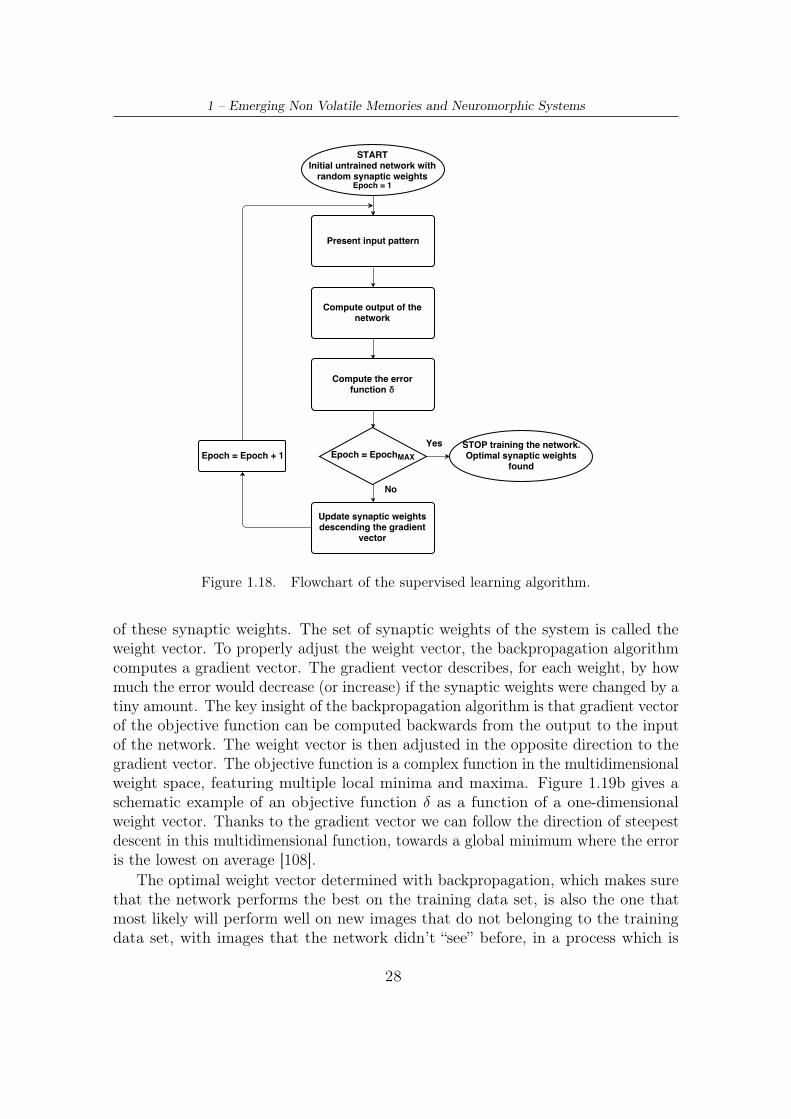
Figure 1.18. Flowchart of the supervised learning algorithm.
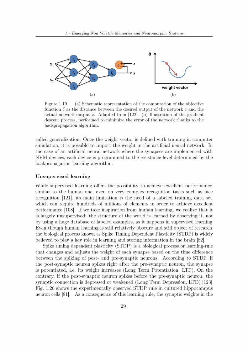
of these synaptic weights. The set of synaptic weights of the system is called theweight vector. To properly adjust the weight vector, the backpropagation algorithmcomputes a gradient vector. The gradient vector describes, for each weight, by howmuch the error would decrease (or increase) if the synaptic weights were changed by atiny amount. The key insight of the backpropagation algorithm is that gradient vectorof the objective function can be computed backwards from the output to the inputof the network. The weight vector is then adjusted in the opposite direction to thegradient vector. The objective function is a complex function in the multidimensionalweight space, featuring multiple local minima and maxima. Figure 1.19b gives aschematic example of an objective function δ as a function of a one-dimensionalweight vector. Thanks to the gradient vector we can follow the direction of steepestdescent in this multidimensional function, towards a global minimum where the erroris the lowest on average [108].
The optimal weight vector determined with backpropagation, which makes surethat the network performs the best on the training data set, is also the one thatmost likely will perform well on new images that do not belonging to the trainingdata set, with images that the network didn’t “seež before, in a process which is
28
1 – Emerging Non Volatile Memories and Neuromorphic Systems
f1
f2
f3
f4
f5
f6
x1
x2
+ δ _
y
z
(a)
δ
weight vector
(b)
Figure 1.19. (a) Schematic representation of the computation of the objectivefunction δ as the distance between the desired output of the network z and theactual network output z. Adapted from [122]. (b) Illustration of the gradientdescent process, performed to minimize the error of the network thanks to thebackpropagation algorithm.
called generalization. Once the weight vector is deőned with training in computersimulation, it is possible to import the weight in the artiőcial neural network. Inthe case of an artiőcial neural network where the synapses are implemented withNVM devices, each device is programmed to the resistance level determined by thebackpropagation learning algorithm.
Unsupervised learning
While supervised learning ofers the possibility to achieve excellent performance,similar to the human one, even on very complex recognition tasks such as facerecognition [121], its main limitation is the need of a labeled training data set,which can require hundreds of millions of elements in order to achieve excellentperformance [108]. If we take inspiration from human learning, we realize that itis largely unsupervised: the structure of the world is learned by observing it, notby using a huge database of labeled examples, as it happens in supervised learning.Even though human learning is still relatively obscure and still object of research,the biological process known as Spike Timing Dependent Plasticity (STDP) is widelybelieved to play a key role in learning and storing information in the brain [82].
Spike timing dependent plasticity (STDP) is a biological process or learning-rulethat changes and adjusts the weight of each synapse based on the time diferencebetween the spiking of post- and pre-synaptic neurons. According to STDP, ifthe post-synaptic neuron spikes right after the pre-synaptic neuron, the synapseis potentiated, i.e. its weight increases (Long Term Potentiation, LTP). On thecontrary, if the post-synaptic neuron spikes before the pre-synaptic neuron, thesynaptic connection is depressed or weakened (Long Term Depression, LTD) [123].Fig. 1.20 shows the experimentally observed STDP rule in cultured hippocampusneuron cells [81]. As a consequence of this learning rule, the synaptic weights in the
29
1 – Emerging Non Volatile Memories and Neuromorphic Systems
Figure 1.20. Experimentally observed STDP rule in cultured hippocampus neurons.Change in Excitatory Post Synaptic Current (EPSC) amplitude is indicative ofchange in synaptic strength or conductance. A spike timing ∆t is defined as timedifference between spikes from the post-synaptic neuron and the pre-synaptic neuron,∆t = tpost − tpre. ∆t < 0 implies LTD while ∆t > 0 implies LTP [81].
brain change over time, and the brain rewires itself with a learning rule that conveysa concept of causality: inputs that might be the cause of the post-synaptic neuron’sexcitation are made even more likely to contribute to neuron spiking in the future,whereas inputs that are not the cause of the post-synaptic spikes are made less likelyto participate in the future.
Unsupervised STDP-inspired learning rules have been successfully proposed inneuromorphic systems with artiőcial NVM synapses. In some examples, STDP isobtained by the overlapping of complex spike shapes [90]. While this approach closelyresembles what is observed in biology, it often requires complicated CMOS circuitryto obtain such complex spike shapes. This approach thus comes at the cost of largerarea and power consumption.
A simpliőed deterministic learning rule, shown in Fig. 1.21a, has been proposedin [101] with multilevel PCRAM synapses. It features the advantage of relying onsimple spike design. A stochastic version of STDP associated to binary NVMs suchas CBRAM, OxRAM and STT-MRAM has been also proposed in [105], [124]ś[126].It is shown in Fig. 1.21b. It is based on a functional equivalence [127] that existsbetween multilevel deterministic synapses and binary probabilistic synapses. When aLTP or LTD occurs, instead of partially changing the conductance of the the synapse,stochastic STDP speciőes probability p < 1 of changing it totally. And if severalNVMs are connected in parallel, a multibit synapse can be emulated.
30
1 – Emerging Non Volatile Memories and Neuromorphic Systems
Bio-inspired computing systems and neuromorphic hardware has a very wide set ofpotential applications. Software based artiőcial neural networks are already beingused eiciently in őelds such as image classiőcation, pattern extraction, face recog-nition, machine learning, machine vision, self-driving cars, robotics, optimization,prediction, natural language processing (NLP) and data-mining [128]ś[134]. Analysisof big-data, web searches, data-center applications, and smart autonomous systemsare new emerging őelds where neuromorphic hardware can play a signiőcant role [63].Neuromorphic concepts are also being explored for defense and security applicationssuch as autonomous navigation, unmanned aerial vehicles, cryptography [135]. Neuro-morphic hardware have also health-care related applications such as future generationprosthetics and brain-machine interfaces [136]. The hardware implementation of deepconvolutional neural network can open the way to power eicient recognition tasks,such as predicting the activity of potential drug molecules [137], analysing data fromparticle accelerator [138], [139], analysing brain circuits [140], and predicting theefects of DNA mutations DNA on gene expression and disease [141], [142]. Deepconvolutional neural networks have also achieved very promising results in naturallanguage understanding [143], particularly topic classiőcation, sentiment analysis,question answering [144] and language translation [145], [146].
1.4 Conclusion
Bio-inspired computing systems where artiőcial neural networks are emulated insoftware or implemented in hardware with traditional von Neumann architectures,such as Digital Signal Processors (DSPs), Graphic processing Units (GPUs) andField-Programmable Gate Arrays (FPGAs), have have shown strong limitationsin terms of power consumption, scalability and reconőgurability [147]. The true
31
1 – Emerging Non Volatile Memories and Neuromorphic Systems
potential of bio-inspired systems can be realized with the implementation on optimizedspecial purpose hardware which can provide direct one-to-one mapping with thelearning algorithms running on it [67]. Emerging resistive memory technologies (asPCM, OxRAM...) are expected to change not only the conventional Von Neumannmemory hierarchy. They will also play a key role in the hardware implementation ofneuromorphic systems, thanks to their exceptional properties of density, scalability,nonvolatility and low power consumption.
32
Chapter 2
Neuromorphic Systems based on
PCRAM synapses
In this chapter, we investigate the use of phase-change random access memory(PCRAM, or PCM) devices as artiőcial synapses. After considering the pro’s andcon’s for the adoption of a multilevel synapse approach, we propose the use of PCMdevice as binary synapse as a simple and eicient solution. We test the functionalityof the proposed approach through large-scale neural network simulations. The useof the proposed binary PCM synapse is studied in a neuromorphic system designedfor complex visual pattern extraction. We explore unsupervised learning adopting aprobabilistic STDP learning rule. Diferent PCM programming schemes for architec-tures with- or without-selector devices are provided. The system-level simulationsshow that such a system can solve a complex real-life video processing problem(vehicle counting) with high recognition rate (>94%) and low power consumption.We also study the impact of the resistance window on the power consumption of thesystem during the learning phase. The problem of resistance drift in PCM devices isalso addressed, and we propose a programming strategy for the mitigation of thisissue.
2.1 Introduction
As discussed in Chapter 1, emerging resistive memories will not only play a key roleto reduce the memory hierarchy gap, in the framework of conventional Von Neumanncomputing. They will also be a key enabling factor for the hardware implementationof artiőcial neural network.
In this chapter, we will focus on the possibility of implementing unsupervisedlearning using PCM devices as synapses. Among the diferent emerging non volatilememory technologies, PCM is one of the most mature. The main advantages of thistechnology are scalability, reliability and low variability [64], [148]ś[152]. Among its
33
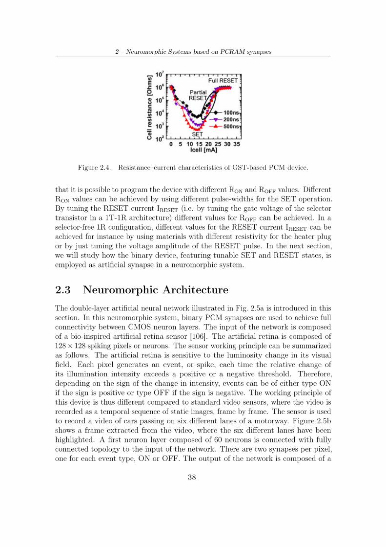
2 – Neuromorphic Systems based on PCRAM synapses
attractive features, the possibility of programming devices to multilevel resistancestates makes PCM an appealing candidate for the realization of artiőcial synapses[153], [154]. For this reason, numerous research groups [101], [104], [153], [155],[156] have investigated the use of PCM devices as artiőcial synapses, adopting themultilevel approach introduced in Section 1.3.2. Numerous neuron spike schemeshave been proposed in the literature to implement unsupervised STDP-based learningwith PCM artiőcial synapses. In this section, we review the main programmingtechniques proposed in the literature.
The scheme proposed in [153] and shown in Fig. 2.1a is a multi-pulse scheme,in which the pre-synaptic spike consists of SET and RESET pulse trains withvarying voltage amplitudes. The post-synaptic spike is an individual pulse which, byoverlapping with one of the pulses of the pre-synaptic pulse train, has the efect ofprogramming the device to a state that depends on the relative timing at which pre-synaptic and post-synaptic spikes have been őred. The weakness of this programmingscheme is the fact that it uses unnecessary pulses in the pre-synaptic spike [64]. Themajority of pulses in the pre-synaptic train is not actually used to program thesynapse, because only one of them overlaps with the post-synaptic spike. These extrapulses might have the efect of disturbing the synapse and other synapses connectedto the same neuron. The large quantity of unnecessary programming pulses is alsorelated to an unwanted large power consumption [65]. This is due to the charging ofinterconnect metal lines, which is not negligible if the considered synapse array islarge. A single programming pulse scheme, proposed in [100], [156] and illustratedin Fig. 2.1b, addresses the drawbacks of the multi-pulse scheme. This approachrelies on the use of a communication signal between the pre-synaptic neuron andthe post-synaptic neuron. One important characteristic of PCM devices is thefact that gradual change of conductance can be achieved using identical pulses onlyin one direction, i.e. from high to low resistance state (Long Term Potentiation,LTP), by gradually increasing of a tiny amount the size of the crystalline regionof the phase change material (Section 1.2.1) applying identical consecutive SETpulses. The RESET process, however, is an abrupt process because it is achievedby melting the whole crystalline region and then quenching it into the amorphousphase. If one wishes to obtain a gradual Long Term Depression (LTD), i.e. graduallyincrease the resistance state from low to high resistance values, RESET pulses withincreasing amplitude need to be used. So the single-pulse programming scheme,even if it avoids unnecessary programming pulses, still requires the generation ofnon-identical voltage pulses, with amplitude changing at every spike. The desiredspike voltage is obtained dynamically as a function of spike timing according to theSTDP rule. In order to implement this functionality in hardware, a complex neurondesign has to be adopted. Each neuron’s circuitry has to keep track of the spiketiming, i.e. the time diference between the last time the neuron spiked and the timeit received the communication signal. Once this time diference is computed, the
desired amplitude of the programming pulse is determined with the STDP rule andthe spike is generated.
In the next subsection, we will discuss how these limitations can be overcome byadopting two devices per synapses with the “2-PCMž synapse approach, at the costof the introduction of a refresh scheme.
2.1.1 The 2-PCM Synapse refresh scheme
The “2-PCM synapsež approach, brieŕy presented in Section 1.3.2, is an alternativesolution proposed for the őrst time in [101], [157] and recently adopted in [104]. Itis schematically illustrated in Fig. 2.2a. An important advantage of the “2-PCMSynapsež approach is the following: since it is based mostly on the crystallizationoperation of PCM devices (SET), it allows deőning a programming methodologythat uses identical neuron spikes, composed of single pulses, to obtain both gradualLTP and LTD, thus requiring a simpler neuron design. This advantage comes atthe cost of a synaptic density reduced by a factor 2, because two PCM devices persynapse are used instead of one.
The conductance of each PCM device gradually increases during the learning,both for LTP and LTD operations. It tends to saturate towards the highest achievableconductance, in which the totality of the active phase change material is crystallized.Therefore, a refresh mechanism is introduced to reduce the conductance of LTPand LTD devices, while keeping the weight of the equivalent synapse unchanged. Aschematic representation of the refresh operation is shown in őgure Fig. 2.2b. As
35
2 – Neuromorphic Systems based on PCRAM synapses
(a)
(b)
Figure 2.2. Illustration of the refresh scheme required by the 2-PCMsynapse approach. Source: [157]
soon as one of the two devices reaches the maximum conductance value, a RESEToperation is performed on both devices. At this point both devices are in the highresistive, amorphous state. In order to recover the equivalent synaptic weight beforethe refresh operation, a series of SET operations is performed on the device that hadthe highest conductance, until the equivalent weight is restored. One has to knowthe average number of conductance levels N obtainable before full crystallizationof the phase-change material in use, for a given SET pulse shape (duration andamplitude). A refresh operation is scheduled after N LTP or LTD operations, usingfor example a simple counter. This approach does not require permanent monitoringof the state of the LTP and LTD devices [65], however this approach still requires arather complex neuron design in order to restore the equivalent synaptic weight ateach refresh operation.
36
2 – Neuromorphic Systems based on PCRAM synapses
(a)
100 101 102 103101
102
103
104
105
106
107
IRESET = 30mA
tRESET = 50ns
ISET = 14mA
tSET = 1µs
# Cycles
Res
ista
nce
(Ω)
ROFF
RON
(b)
Figure 2.3. (a) Scheme of the studied GST PCM device (top) and cross-sectionTEM image (bottom) [23]. (a) Experimental results of 103 SET-RESET cycles.
In the next sections, we will hence discuss how PCM devices can be used inbinary mode in order to simplify the programming scheme and therefore avoid thedrawbacks of the multilevel approach.
2.2 PCM binary synapse
We propose here a diferent approach for PCM synapses, i.e. a binary probabilisticone, where only two states are used for the synaptic weights and the switching ofthe device between these two states is governed by a probabilistic learning rule.This study was carried out to simplify system programming by avoiding the refreshoperation previously required in the 2-PCM approach, and to optimize the synapticpower consumption.
In order to extract the characteristics of PCM devices operated in binary modeand be able to model the PCM synapses in artiőcial neural network simulations,electrical characterization was performed. PCM devices composed of a 100 nm thickGe2Sb2Te5 (GST) phase-change layer were studied. The phase change materialwas deposited at room temperature by plasma-assisted sputtering on a cylindricaltungsten heater plug with a diameter of 300 nm. Figure 2.3a shows a TransmissionElectron Microscopy (TEM) image of the studied devices. Devices could be repeatedlyswitched between low resistance (ON) and high resistance (OFF) states with SETand RESET programming pulses. Figure 2.3b shows the switching operation betweenON and OFF states for 103 cycles using the programming conditions indicated inőgure.
Based on the ResistanceśCurrent (RśI) characteristic shown in Fig. 2.4, it appears
37
2 – Neuromorphic Systems based on PCRAM synapses
Figure 2.4. Resistance–current characteristics of GST-based PCM device.
that it is possible to program the device with diferent RON and ROFF values. DiferentRON values can be achieved by using diferent pulse-widths for the SET operation.By tuning the RESET current IRESET (i.e. by tuning the gate voltage of the selectortransistor in a 1T-1R architecture) diferent values for ROFF can be achieved. In aselector-free 1R conőguration, diferent values for the RESET current IRESET can beachieved for instance by using materials with diferent resistivity for the heater plugor by just tuning the voltage amplitude of the RESET pulse. In the next section,we will study how the binary device, featuring tunable SET and RESET states, isemployed as artiőcial synapse in a neuromorphic system.
2.3 Neuromorphic Architecture
The double-layer artiőcial neural network illustrated in Fig. 2.5a is introduced in thissection. In this neuromorphic system, binary PCM synapses are used to achieve fullconnectivity between CMOS neuron layers. The input of the network is composedof a bio-inspired artiőcial retina sensor [106]. The artiőcial retina is composed of128× 128 spiking pixels or neurons. The sensor working principle can be summarizedas follows. The artiőcial retina is sensitive to the luminosity change in its visualőeld. Each pixel generates an event, or spike, each time the relative change ofits illumination intensity exceeds a positive or a negative threshold. Therefore,depending on the sign of the change in intensity, events can be of either type ONif the sign is positive or type OFF if the sign is negative. The working principle ofthis device is thus diferent compared to standard video sensors, where the video isrecorded as a temporal sequence of static images, frame by frame. The sensor is usedto record a video of cars passing on six diferent lanes of a motorway. Figure 2.5bshows a frame extracted from the video, where the six diferent lanes have beenhighlighted. A őrst neuron layer composed of 60 neurons is connected with fullyconnected topology to the input of the network. There are two synapses per pixel,one for each event type, ON or OFF. The output of the network is composed of a
38
2 – Neuromorphic Systems based on PCRAM synapses
(a) (b)
Figure 2.5. (a) Schematic of the fully connected neuromorphic system studied insimulation. (b) An example of one of the frames of the input video, showing carspassing on multiple lanes of a motorway. The separation between lanes (in yellowcolor) has been added to illustrate the distinction among different lanes and is notpresent in the original input video.
second layer of 10 neurons, where each neuron is connected to each neuron of theprevious layer via one PCM synapse. The total number of synapses in the studiedsystem is thus Nsynapses = 2 · 128 · 128 · 60 + 60 · 10 = 1 966 680.
The neuromorphic system here described is used to detect cars passing on diferentlanes: when a car is driving on a given lane, the corresponding output neuron isactivated. This allows to extract information about when and which lane a caris driving on. In order to make sure that diferent neurons become sensitive todiferent lanes, avoiding that one neuron becomes sensitive to the full set of lanes,a particular learning strategy is adopted, i.e. competitive learning. Competitivelearning is obtained by implementing lateral inhibition, i.e. when a post-synapticneuron őres, the integration of incoming spikes in the other post-synaptic neuronsof the same layer is disabled [158]. Therefore, we avoid that all neurons becomesensitive to the full input frame and we make sure to diferentiate the neuronssensitivity. This neuromorphic system is analogous to that proposed in [101] anddescribed in Section 1.3.3. The diference is that in this approach, only 1 PCM deviceper synapse is used, and the learning rule has been adapted to the new proposedsynapse. The neuromorphic system proposed here is associated to a probabilisticSTDP learning rule. Its adoption is based on a functional equivalence [127] existingbetween a multilevel deterministic learning rule and a binary probabilistic one. Thisequivalence is schematically represented in Fig. 2.6: when a long term potentiation ordepression occurs, instead of gradually changing the conductance of the the synapsewith probability p = 1, probabilistic STDP has a probability p < 1 of switchingthe synaptic totally from one state to the other. A similar approach has been
39
2 – Neuromorphic Systems based on PCRAM synapses
Figure 2.6. Illustration of the equivalence existing between multi-level determin-istic and binary probabilistic synapses. p indicates the probability of change inconductance or switching. Adapted from [105].
Figure 2.7. Binary probabilistic learning rule adopted for the simulations.
adopted in previous works, such as in [105], [159]ś[161]. This approach is motivatedby biology research [162], presenting some evidence that STDP learning could bein part a stochastic process. As shown in the learning rule scheme of Fig. 2.7,if the time diference between the spike of a post-synaptic neuron and the spikeof a pre-synaptic neuron is smaller than the long term potentiation (LTP) timewindow tLTP, then the PCM synapse has a given probability to switch to the ONstate (LTP or synaptic-potentiation). Otherwise, the PCM device has a distinctgiven probability to switch to the OFF state (LTD or synaptic depression). Neuronparameters, including switching probability and spike timing values shown in Fig. 2.7,have been determined using the genetic evolution algorithm described in [163]. Thedesired switching probabilities can be enforced in the system extrinsically by using aPseudo-Random Number Generator (PRNG) circuit, similarly to [105]. The PRNGcircuit controls the probability of LTP and LTD with a 2-bit signal.
In order to implement the full connectivity of the CMOS neuron layers in theartiőcial neural network, we suggest two possible architectures, shown in Figs. 2.8a
40
2 – Neuromorphic Systems based on PCRAM synapses
and 2.8b: a matrix structure with a selector transistor for each PCM device anda selector-free crossbar structure. The crossbar (selector-free) architecture ofersthe highest possible integration density, however it can be only implemented ifthe programming conditions for the chosen PCM technology ensure that there areno unwanted device disturbs (see Section 2.3.1). On the other hand, the matrixarchitecture, while requiring more area for selectors, is not sensitive to disturb issues.It should be noted that the two architectures and programming schemes are validnot only for PCM technology-based synapses, but can be extended to other unipolardevices, as for example unipolar oxide-based resistive memories [164] described inSection 1.2.4.
2.3.1 Operation of the system
The operation of the proposed neuromorphic system can be classiőed in two diferentmodes: learning-mode and read-mode.
Learning mode
In learning mode the synaptic programming is enabled, following the STDP rule.The spiking activity recorded with the artiőcial retina is presented to the network fora period of time tLEARNING = 680 s. The network learns from data in unsupervisedfashion, and diferent output neurons become sensitive to the passing of car ondiferent lanes. It is only during the learning mode that the synaptic weights ischanged with SET and RESET operations.
Two diferent programming schemes are proposed for the two diferent studiedarchitectures:
• Programming scheme for matrix structure with selectors (Fig. 2.8a). In thelearning mode, when a post-synaptic neuron őres, all the incoming synapsesare activated by means of the select transistor. Concurrently, a write-modesignal is sent to all pre-synaptic neurons so that the following happens: if apre-synaptic neuron őred recently, i.e. during the LTP time window, a VSET
signal has a pLTP probability to be applied to the device. On the contrary, ifthe last activity of the pre-synaptic neuron is outside the LTP window, there isa pLTD probability for a reset pulse to be applied. In the example of Fig. 2.8a),the following scenario is represented. The post-synaptic neuron in the őrstrow of the memory array őres. As a consequence, all the PCM devices inthe őrst row of the matrix are selected, while all other rows are not selected.The post-synaptic sends a write-mode signal to the pre-synaptic neurons. Thepre-synaptic neurons can be categorized in two categories, labeled as “Inputžand “No inputž. The pre-synaptic neurons marked as “Inputž received an inputspike in the recent past, within the LTP time-window ∆t deőned by the STDP
41
2 – Neuromorphic Systems based on PCRAM synapses
rule. On the contrary, the pre-synaptic neurons marked as “No inputž didnot receive any input spike within the LTP window. The “Inputž neurons arethus possible candidates for performing an LTP operation. The actual decisionwhether an LTP operation actually occurs or not is made according to the valueof the őrst bit of the 2-bit signal from the PRNG block. If the bit is equal to 1(as in the case of the őrst column), then LTP occurs, by applying a SET voltagewith amplitude VSET. The conductance G of the PCM synapse thus increases.If the bit is equal to 0 (third column), no programming pulse is applied, sothe conductance is unchanged. Similarly, the “No inputž neurons are possiblecandidate for performing an LTD operation. The actual decision whether anLTD operation actually occurs or not is made according to the value of thesecond bit of the 2-bit signal from the PRNG block. If the bit is equal to 1(as in the case of the fourth column), then LTD occurs, by applying a RESETvoltage with amplitude VRESET. The conductance G of the PCM synapse thusdecreases. If the bit is equal to 0 (second column), no programming pulse isapplied, so the conductance is unchanged.
• Programming scheme for selector-free crossbar structure (Fig. 2.8b). Whenevera post-synaptic neuron őres, a feedback pulse −1
2VRESET is fed back to all
the synapses connected to it on the same row. If 1
2VRESET < VSET, the signal
does not afect the resistive state of the connected synapses as its amplitudeis less than the programming threshold. At the same time, a write-modesignal is provided to all pre-synaptic neurons so that they will őre accordingto the probabilities given by the STDP rule and implemented by means ofthe PRNG block. If a pre-synaptic neuron was active in the LTP window,there is a pLTP probability for a V∆ = VSET − 1
2VRESET signal to be őred. It
will interact with the feedback signal so that the actual voltage drop acrossthe corresponding synapse is VSET = V∆ − (−1
2VRESET) and the synapse is
switched to the ON state. The amplitude of the V∆ pulse on its own is not largeenough to program the other connected synapses. If a pre-synaptic neuron’s lastactivity is outside the LTP time window, its output will be a +1
2VRESET pulse
with a pLTD probability or a −1
2VRESET pulse with a (1−pLTD) probability. The
positive pulse will interact with the feedback resulting in a pulse of amplitudeVRESET = +1
2VRESET − (−1
2VRESET), while the negative pulse will result in a
voltage drop across the device equal to 0V, thus keeping the resistance of thecell unaltered.
Read mode
After the learning phase, the learning achieved by the network is evaluated in readmode by showing to the network an 85 s long video recording. When the circuit isin read mode, the synaptic programming is disabled. Spiking activity propagates
42
2 – Neuromorphic Systems based on PCRAM synapses
(a) Architecture with selector device
(b) Selector-free architecture
Figure 2.8. (a) Architecture with selector device and (b) selector-free architecture.
through the network, from the input to the output layer. SET and RESET operationsare not performed. Only spikes, consisting of read pulses, occur. Whenever an inputevent occurs, a read voltage pulse (or spike) is applied by the pre-synaptic neuronsacross the PCM synapses. In the architecture with selector, all transistors are turnedon by applying a select voltage on the gate terminals. The input events contribute tothe current integration of the post-synaptic neurons according to the weight (i.e. theresistive state) of the synaptic connections. When the integration threshold of apost-synaptic neuron is reached, a spike is fed forward to the next neural layer orthe output of the circuit.
43
2 – Neuromorphic Systems based on PCRAM synapses
0 200 400 600 800 1000101
102
103
104
105
106
107
IRESET = 30 mA
tRESET = 50 ns
ISET = 14 mAtSET = 1µs
# Cycles
Cel
lR
esis
tanc
e(Ω
)
Figure 2.9. Simulated values of the binary PCM synapses resistance over 1000 cycles.
2.3.2 System performance
We tested the functionality of the proposed system with the event-driven “XNETžsimulation tool for spiking neural networks presented in details in [165], [166]. Thesynapses were modeled by implementing lognormal distributions with mean values forRON=110Ω, ROFF=1.06MΩ extracted from data presented in Fig. 2.3b. Figure 2.9shows the simulated values of binary PCM devices over 1000 cycles. In all simulationsa 10% device-to-device standard deviation was implemented for both resistive states.A 5% cycle-to-cycle standard deviation was also implemented for RON and a 10%cycle-to-cycle standard deviation was implemented for ROFF. The activity of eachoutput neuron is compared to a reference data set, in which the timing of the passingof cars in each lane is labeled by hand. In this way, a score or detection rate can becomputed for each output neuron with respect to the reference data of each lane.The detection rate takes into account both false negatives, (i.e. missed cars) andfalse positives, i.e. neuron spiking even if no car passed on the considered lane ata given time. Since there are 10 output neurons and 6 lanes, the 6 best matchingneuron-lane couples are selected and taken into account for the score computation. InTable 2.1 the score of the output neurons of the neuromorphic system here proposedis presented and compared to the results previously obtained with the “2-PCMžmulti-level deterministic approach reported in [101]. The őnal sensitivity patterns ofthe 6 neurons that became sensitive to the 6 lanes are shown in Fig. 2.10. Cars inthe őrst and sixth lanes, being at the edge of the visual őeld of the retina, activateless pixels compared to those on other lanes. The detection rate for the centrallanes is equal to 95% on average, and it is comparable to the results obtained withthe multilevel-deterministic approach shown in [101]. This conőrms the functionalequivalence between the two systems. The score obtained by the correspondingneurons is low (< 85%), so it has been omitted. In the next section, we will describehow the choice of programming conditions, and the corresponding values of RON and
44
2 – Neuromorphic Systems based on PCRAM synapses
detection rate (%)
lane2śPCM ref. [101]
Binary Probabilistic
[this work]
1st N.A. N.A.
2nd 100 97
3rd 89 93
4th 89 94
5th 96 96
6th N.A. N.A.
Total synapticpower consumption 112 µW 73 µW
Table 2.1. Cars detection rate by lane as obtained with the system based on themultilevel-deterministic PCM synapses [101] and the binary probabilistic PCMsynapses presented in this chapter.
Figure 2.10. Sensitivity maps of 6 neurons at the end of learning phase. Theneurons became selective to cars passing on the central lanes.
ROFF, afect the power consumption of the system.
2.4 Power consumption analysis
As discussed in Section 2.2, by varying the programming conditions for the PCMsynapses it is possible to obtain diferent values for RON and ROFF. Based on thisconsideration, a set of parametric simulations has been carried out in order to studythe impact of the PCM programming conditions on synaptic power consumption, andprovide guidelines to optimize the power consumption in the studied neuromorphicsystem. First, a set of simulations has been performed changing the SET conditionstogether with the corresponding RON values, while keeping ROFF ≈ 1MΩ constant.Speciőcally, the SET pulse width has been varied from tSET = 100 ns up to tSET = 1 µs,with corresponding RON values ranging from RON≈100Ω to RON≈10 kΩ. Then, a
45
2 – Neuromorphic Systems based on PCRAM synapses
102103104
20
40
60
80
decreasing ROFF
increasing RON
ROFF/RON
RE
SET
even
ts/
SET
even
ts
Figure 2.11. Ratio between thenumber of RESET and SET eventsas a function of the resistance win-dow ROFF/RON.
1.5
1.55
1.6
1.65
1.7
·107
RE
SET
even
ts
102103104
4.4
4.6
4.8
5·105
ROFF/RON
SET
even
ts
RESET eventsSET events
Figure 2.12. Number of SET andRESET events as functions of theresistance window ROFF/RON.
set of simulations changing RESET conditions and the corresponding ROFF valueshas been carried out. The reset current has been varied from IRESET=17mA toIRESET=30mA. In this set of simulations, the low resistance state value RON≈100Ωhas been kept constant. In all simulations, the system remained functional and theaverage detection rate was ≥ 94%. In the next section the results of the parametricsimulations in term of power consumption are discussed, considering both learningmode and read mode.
2.4.1 Learning mode power consumption
First, power consumption in learning mode has been evaluated. In order to do so,the number of SET and RESET events performed during the learning phase hasbeen recorded, during the learning time tLEARNING = 680 s.
Section 2.4.1 shows that the ratio between the total number of RESET and SETevents remains constant when the resistance window, deőned as the ratio ROFF/RON,changes. Indeed, this means that the programming activity is dominated by theinput stimuli and the STDP learning rule. However, as shown in Section 2.4.1, theabsolute number of both SET and RESET events increases when the resistancewindow is reduced. This can be explained with the fact that, when the resistancewindow is reduced, the ROFF value is closer to the RON value. So, the contributionof the synapses in OFF state to the current integration at the post-synaptic neuronsis larger. This means that the threshold of the integrate and őre neuron is reachedmore frequently. As a consequence, the number of times that neurons őre is larger,leading to an increased number of LTP and LTD events.
46
2 – Neuromorphic Systems based on PCRAM synapses
Once the number of SET (NSET) and RESET operations (NRESET is known, itis possible to estimate the power consumption associated to the SET and RESETswitching events, i.e. the synaptic power consumption PLEARNING during the learningtime tLEARNING = 680 s, using the following approximated formulas:
where VSET (VRESET), ISET (IRESET) and tSET (tRESET) are the voltage amplitude,current and time width associated to each SET (RESET) programming pulse.
Section 2.4.1 shows that when ROFF is decreased while keeping RON őxed (redcurve) it is possible to reduce the synaptic programming power during learning by32%. This is explained by the fact that smaller current values are required to obtainsmaller ROFF values. It should be noted that the high current values consideredin these simulations, in the order of tens of mA, are due to the large PCM teststructures (300 nm heater plug) studied in this work. In ultra-scaled state of the artdevices [29], the reset current can be reduced to µA, so giving rise to programmingpower in the order of nW. Weakening the SET state (increasing RON, blue curve)does not translate into a reduction of the programming power. This is explained bytwo reasons: 1) the STDP rule is strongly dominated by LTD, i.e. RESET operations,rather than SET operations; 2) when the resistance window is decreased, the numberof RESET events increases (see Section 2.4.1). So, the efect of weakening the SETconditions gets compensated by the increased number of RESET events.
2.4.2 Read mode power consumption
In order to compute the power consumption associated to the read mode operation,the system spiking activity has been recorded during the read-mode time, withduration tTEST = 85 s. Total read energy has been computed as the sum of theenergy associated to each read pulse or spike.
EREAD =∑
i
V 2READ · 1
Ri
· tREAD (2.5)
PREAD =EREAD
tTEST
, (2.6)
where VREAD is the amplitude of the read spikes, tREAD is the read pulse widthand Ri is the resistance of each synapse, that can be equal to either RON or ROFF.It should be noted that the variation of the RON values plays a bigger role in the
47
2 – Neuromorphic Systems based on PCRAM synapses
102 103 104
RON (Ω)
104105106
50
55
60
65
70
75
ROFF (Ω)
Pro
gram
min
gpo
wer
(µW
)
RONROFF
Figure 2.13. Programming power as a function of decreasingROFF (RON=110Ω constant, red line, squares) and increasing RON
(ROFF=1.06MΩ constant, blue line, circles).
determination of the power consumption in read mode, as it determines the mostimportant contribution to the current ŕowing into the synapses at each read pulsesince RON is orders of magnitude smaller than ROFF. As shown in Section 2.4.2,increasing the RON value (blue curve), it is possible to reduce the power consumptionfor read operations by 99%. Variation of ROFF value, on the other hand, determinesa negligible variation in the read mode power consumption.
2.5 Resistance drift
As discussed in Section 1.2.1, one of the main issues of PCM technology is theresistance drift, which is a change of the device resistance value over time. Consideringthe devices in the RESET state, structural relaxation occurs in the amorphous phaseregions of the calchogenide material [167]. As a consequence, the resistance of PCMdevice increases with time. Resistance drift in the crystalline SET state of GST-basedPCMs is shown to be much smaller than in the amorphous phase [167], [168].
Resistance drift has a limited impact during the learning phase of a neuromorphicsystem. In fact during learning, because of the STDP learning implementation,spiking activity and corresponding LTP and LTD events dynamically change asa function of the resistive state of the synapses [65]. A resistance drift towardshigh resistance state is balanced-out by an increased LTP activity, which brings the
48
2 – Neuromorphic Systems based on PCRAM synapses
102 103 104
RON (Ω)
104105106
0
100
200
300
400
ROFF (Ω)
Rea
dpo
wer
(nW
)
ROFFRON
Figure 2.14. Read power as a function of decreasing ROFF (RON=110Ω constant,red line, squares) and increasing RON (ROFF=1.06MΩ constant, blue line, circles).
resistance of the devices back to the low resistance state. So the main efect of driftduring learning phase is a delay in the learning time.
However, resistance drift efect might be much more detrimental in the readmode operation of the neuromorphic system, when the uncontrolled change in theresistance state of the synapses cannot be compensated by the plastic programmingactivity characteristic of the learning phase. For this reason, the performance ofsystems featuring drifting synapses might change over time, compared to the originalperformance of the network obtained right after the learning phase.
Based on these considerations, XNET learning simulations of the car videoapplication discussed in the previous sections have been conducted. This study hasbeen performed using both multilevel deterministic (2-PCM) and binary probabilisticapproaches. These simulations have been carried out to evaluate how many devices,at the end of the learning phase, are in the high resistance state and thus in theresistance range afected by drift. Figure 2.15a and Fig. 2.15b show the őnal synapticresistance distributions of the PCM devices, corresponding to the multilevel andbinary PCM synapses, respectively.
Results show that, in the case of the 2-PCM synapse approach (Fig. 2.15a), about60% of the devices are in the SET state, i.e. in the resistance range not afected bydrift. This is due to the fact that, in the 2-PCM synapse approach, both potentiation(LTP) and depression (LTD) are obtained by SET events. This result is valid evenif the learning rule is predominantly governed by LTD as in the studied case. So,
49
2 – Neuromorphic Systems based on PCRAM synapses
(a) (b)
Figure 2.15. Comparison of the distributions of synaptic resistance states for(a) the 2-PCM synapse approach and (b) binary PCM approach at the end ofthe visual learning simulation.
at the end of the learning phase, the majority of PCM devices are programmed inthe low resistance range which is rather immune to the drift problematic [32], [168],[169]. For this reason, the 2-PCM synapse approach seems inherently robust to thedrift problematic. However, a non-negligible amount of devices (about 40%) still liesin the region which is afected by drift. When the learning is over and the systemis used in read mode, the resistance value of these synapses will change over time.This implies that the response of the network will also change over time, togetherwith the performance of the network in read mode, which is an undesired efect.
In the case of the binary PCM synapses shown in Fig. 2.15b it appears that, atthe end of the learning phase 97%, of the devices is in the RESET state, i.e. in theresistance state which is afected by drift. This result suggests that in theory theproblem of drift would severely afect neuromorphic systems based on the binaryPCM approach. Section 2.5.1 presents a programming strategy that we conceived inorder to mitigate the problem of drift.
2.5.1 Drift mitigation strategy
In the case of binary PCM Synapse architecture the impact of drift can be fullymitigated if the reset state of the PCM devices is tuned carefully to a partial RESETstates, where the drift problem is negligible. In order to evaluate this strategy, weperformed XNET simulations for the Binary-PCM synapse architecture using 3diferent PCM RESET states, keeping the SET state constant with RON≈ 600Ω:
1. negligible drift region, mean ROFF = 20 kΩ;
2. low drift region, mean ROFF = 30 kΩ;
3. high drift region, mean ROFF = 123 kΩ.
50
2 – Neuromorphic Systems based on PCRAM synapses
Figure 2.16. Distribution of synapses in RESET state for the binary PCM synapseapproach with mean ROFF values of 20 kΩ, 30 kΩ and 123 kΩ.
Table 2.2. Comparison of learning statistics for the different simu-lated architectures [170].
The őnal synaptic resistance distributions for the PCM synapses in the 3 cases areshown in Fig. 2.16. Table 2.2 compares the learning statistics for the multilevel2-PCM and the binary PCM approach with partial RESET states immune to drift.The energy consumption decreases in the case of binary-PCM synapse as the currentrequired to program partial-reset states (20 kΩ and 30 kΩ) is much smaller comparedto the current required to program the RESET strong reset state (128 kΩ). Duringread mode, the power consumption of the binary PCM approach is much smallerbecause, at the end of learning, the majority of the devices is in the high resistancestate, contrary to the 2-PCM approach, as shown in Figs. 2.15a and 2.15b.
51
2 – Neuromorphic Systems based on PCRAM synapses
(a) (b)
Figure 2.17. (a) Schematic representation of the scaled wall storage structurePCM device [25]. (b) SET and RESET experiment for 106 cycles on scaledwall storage PCM device.
2.6 Simulations using scaled devices
In the previous sections, we carried out our analysis based on electrical results obtainedfrom test devices featuring a large heater plug. The corresponding programmingcurrent is thus very large, in the order of tens of mA. In this section, we will showhow, using state-of-the-art PCM devices, it is possible to reduce the programmingcurrent and, as a consequence, the synaptic programming energy. For this reason,electrical characterization has been performed on “wall storagež PCM memory cells,fabricated in 90 nm technology node in the framework of the R&D project betweenSTMicroelectronics and CEA-LETI [25]. The device structure is schematicallyrepresented in Fig. 2.17a. The smallest feature size of the heater is not limited by thephotolithographic resolution. The active phase-change material is GST. Figure 2.17bshows the RON and ROFF values for one device corresponding to 106 SET-RESETcycles. The experimental resistance values of the PCM devices have been used tomodel, in XNET simulation, the resistance distributions of the PCM synapses duringthe learning of the car video. The characteristics of the STDP learning rule have alsobeen optimized by genetic evolution algorithm [163] in order to adapt the learningto the new synaptic distributions. Speciőcally, the LTP time window and LTDprobabilities have been increased from tLTP = 7.6ms, pLTD = 0.11 to tLTP = 13.4ms,pLTD = 0.21. Therefore, the network activity is larger in terms of SET and RESETevents in the case of the wall storage device. Simulation results are presented inTable 2.3, where the learning statistics of the two studied neuromorphic systems,with large heater synapses and scaled wall storage synapses, are compared. Resultsshow that, even if the programming activity is increased in the case of the scaledsynapses, the total programming energy associated to SET and RESET events is
Table 2.3. Comparison of PCM learning statistics obtained for large heater devicesand scaled wall storage devices.
reduced by one order of magnitude, from 70 µW to 7 µW. Furthermore, the powerconsumption associated to the read mode is reduced by three orders of magnitude,from 64 nW to 0.5 nW. This is due to the smaller current associated to the readoperations with the scaled devices. The most important contribution to the to thetotal read current is in fact given by the read operations on devices in the SETstate, because their resistance is smaller compared to the RESET state. Since forthe scaled devices the mean RON is much larger compared to the heater plug devices(57 kΩ vs. 110Ω), the resulting read current is smaller.
2.7 Conclusion
In this chapter, we investigated the use of PCM devices as synapses in a fullyconnected artiőcial neural network. We presented the limitations associated to theuse of the multilevel synapse approach. Therefore, driven by the motivation toovercome the limitations associated to the multilevel approach, we explored the useof PCM synapses in binary mode. Based on the results obtained from electrical
53
2 – Neuromorphic Systems based on PCRAM synapses
characterization, we performed simulations of a large scale artiőcial neural networkfor complex visual application, tuning the resistance levels of the SET and RESETstates according to the selected programming conditions. Programming schemesfor architectures with- or without-selector devices are provided. The proposedprogramming schemes avoid the use of complex refresh schemes and unnecessaryprogramming pulses required by multilevel PCM synapses. Simulation results showthat the learning mode power consumption associated to the studied neuromoprphiccan be dramatically reduced if the RESET state of the PCM devices is tuned to arelatively low resistance. Read-mode power consumption, on the other hand, can beminimized by increasing the resistance values for both SET and RESET states of thePCM devices. We also investigated the issue of PCM resistance drift and we proposeda strategy to mitigate this problem. We also observed that, using scaled devices,it is possible to dramatically reduce the power consumption thanks to the smallerprogramming current. In conclusion, we successfully demonstrated the interest ofusing PCM devices in binary mode in a neuromorphic system for visual applications.
54
Chapter 3
OxRAM technology: failure
mechanisms and variability
In this chapter, the main features of the HfO2-based OxRAM technology, oneof the most promising emerging non-volatile memory (NVM) technologies, arepresented. Experimental results on endurance failure mechanisms are discussedand a programming methodology to improve endurance at low operating currentis proposed. A physical model able to explain OxRAM variability in both LowResistance State (LRS) and High Resistance State (HRS) is presented. This studyis carried out with a dual aim. From the point of view of conventional memoryapplications, variability is indeed one of the limiting factors for the adoption ofOxRAM technology in commercial products. The understanding of the source ofresistance variations of OxRAM can thus give guidelines to reduce this issue. Fromthe point of view of neuromorphic computing, OxRAM devices are an ideal candidatefor the implementation of artiőcial synapses. The development of a model able toreproduce device variability for a wide range of programming conditions can be usedto study the impact of synaptic variability at the system level.
3.1 Device structure
The devices studied in this chapter feature a metal-insulator-metal (MIM) structurecomposed of an HfO2 layer between a TiN/Ti top electrode and a TiN bottomelectrode (Fig. 3.1) [171]. A bitcell is composed of 1 Transistor − 1 Resistor (1T1R)structure, where the access transistor is used to select the cell when integrated intoan array and limit the current ŕowing through the device during programming. Theelectrical characterization was performed on both 1T1R bitcells and on a 28 nmCMOS digital testchip that contains 16 Circuits Under Test (CUTs) of 1 kb each,plus a digital controller (Fig. 3.2a,b), fabricated in the framework of an R&D projectbetween STMicroelectronics and CEA-LETI [172]ś[174].
55
3 – OxRAM technology: failure mechanisms and variability
Figure 3.1. 1T-1R device schematic.
(a) (b)
Figure 3.2. (a) SEM cross section of CMOS 28 nm stack including MIM device, (b)16 kb circuit demonstrator layout [172].
3.2 Device operation
Typical I−V characteristics and switching behavior of a 1T1R bitcell are shown inFig. 3.3. The operation of the device is bipolar, i.e. opposite voltage is necessary forthe switching of the device from low to high resistance state and vice versa. Devicesinitially in Pristine Resistance State (PRS), featuring very high resistances, typicallylarger than 1GΩ, are subjected to an electroforming operation (forming) by applyinga positive voltage (≈ 2V) across the device (red curve). This operation induces a softbreakdown of the oxide layer thus creating a conductive őlament (CF) rich in oxygenvacancies (VO) [48]. After the forming operation, the device is established in the LowResistance State (LRS). The RESET operation, consisting in the application of anopposite voltage VRESET across the device, partially disrupts the CF by recombinationof oxygen vacancies with oxygen ions, hence leading to the High Resistance State(HRS) (green curve). In the SET operation, a positive voltage is applied on the topelectrode (blue curve). This reforms the CF, bringing the device back in LRS. After
56
3 – OxRAM technology: failure mechanisms and variability
the initial forming step, the device can be switched multiple times between LRSand HRS with RESET and SET operations as schematically depicted in Fig. 3.4.Table 3.1 reports the three main programming parameters that are associated to thethree programming operations. After each SET and RESET operation, a low-őeldmeasurement of the device resistance is performed (READ operation): a voltageVREAD = 0.1V is applied on the top electrode and the corresponding read currentŕowing through the device is measured.
3.3 Endurance: failure mechanisms
Endurance is deőned as the number of SET/RESET cycles that a device can sustainwhile remaining functional, i.e. maintaining a signiőcant resistance contrast betweenthe ON/OFF states. When SET or RESET operations are not efective to switchthe resistance state of the devices, the device is not functional and a failure occurs.
In the context of the use of OxRAM devices as artiőcial synapses, a good enduranceis of great importance, because it allows a longer learning phase in a neuromorphicsystem, if the application requires a long learning phase. At the same time, it is
57
3 – OxRAM technology: failure mechanisms and variability
Table 3.1. Parameters associated to the three programming operationsof OxRAM devices
also important to reduce the energy required for SET and RESET operations, inorder to reduce power consumption during device operation. The impact of SETand RESET operations on endurance has been thoroughly investigated in literature.Chen et al. [175] provided experimental evidence of two opposite endurance failuremechanisms, observed as a function of the SET programming current IC SET for agiven reset voltage VRESET. The experiments were carried out on a memory stacksimilar to the one studied in this thesis, composed of TiN/Hf/HfO2/TiN [175].
1. Low programming current IC SET: an endurance failure with resistance stuckat HRS, with resistance values larger than 10MΩ. This value is closer to pre-forming resistance values than to typical HRS resistance obtained after RESEToperation. SET operations are not useful anymore to bring the resistance ofthe device back to LRS. An example is reported in Fig. 3.5a.
2. High programming current IC SET: in this case, the failure occurs with theresistance of the device stuck at LRS. The RESET operation is not functional tobring the device resistance back to HRS. An example of this type of enduranceis presented in Fig. 3.5b.
Chen et al. [175] also demonstrated that, by carefully balancing SET and RESETconditions, it is possible to improve the endurance as shown in Fig. 3.5c, achievingan endurance larger than 1010 SET-RESET cycles. This however implies that, fora given value of VRESET, the value of IC SET must be increased to an intermediatevalue. This leads to an increased power consumption with respect to the conditionsdescribed in point 1.
In this work, we explore an alternative approach to improve endurance withoutincreasing the power consumption during cycling. We start from the observation
58
3 – OxRAM technology: failure mechanisms and variability
(a) (b)
(c)
Figure 3.5. Example of: (a) endurance failure mechanism 1, where the resistance isstuck at pre-forming, high resistive state; (b) endurance failure mechanism 2, wherethe resistance is stuck at low resistive state. (c) Selecting balanced SET/RESETconditions allows improving the endurance but requires increasing IC SET, thusincreasing power consumption. Adapted from [175].
that, in order to reduce the average power consumption P , it is necessary to use anIC SET as small as possible for a given reset voltage VRESET and programming pulsewidth t, as shown in Fig. 3.6. The approximated equations that have been used toestimate the average power consumption are the following:
ESET ≈ IC SET · VSET · t (3.1)ERESET ≈ IRESET · VRESET · t (3.2)ETOT = ESET + ERESET (3.3)
P =ETOT
T(3.4)
where ESET and ERESET are the energies required for SET and RESET operations,respectively. IC SET is the compliance current imposed by the select transistor duringthe SET operation. IRESET is the current ŕowing through the device during RESET,and assumed equal to IC SET, according to the universal RESET characteristics ofOxRAM devices [176]. VSET = 1V and VRESET are the voltage drops across the 1T1R
59
3 – OxRAM technology: failure mechanisms and variability
Figure 3.6. Estimated switching power as a function of IC SET, obtained for 3different values of VRESET, for a pulse width of t = 100 ns and t = 1 µs.
structure during SET and RESET operations, respectively. T is the time frameover which the average is computed, assumed equal to 1 s. As a consequence, theendurance failure mechanism that will be encountered is mechanism 1, i.e. resistancestuck at HRS.
Fig. 3.7 shows the typical bitcell behavior during an endurance experiment. Theprogramming current is ≈ 230 µA. If long pulse widths equal to 1 µs for both RESETand SET are used, no failure occurs and more than 108 cycles endurance can beachieved (Fig. 3.7 (a)). If shorter pulses with height 1 V and width 100 ns are used,a failure in endurance is observed after around 105 cycles, with the resistance of thedevice stuck at high resistance state Fig. 3.7 (b). The SET failure is an evidence ofthe unbalance between RESET and SET conditions, which is accentuated at shortprogramming time. Speciőcally, the value of IC SET ≈ 230 µA is too low for theadopted VRESET = 1.3V at t = 100 ns.
While the role of SET and RESET programming conditions has been discussedin literature in depth [175], little importance has been given to the role of theFORMING operation on the endurance performance. We can schematically representour hypothesis of what happens in the OxRAM device during FORMING and őrstRESET operation with the simple schematic pictures reported in Fig. 3.8. DuringFORMING operation, the oxygen vacancy-rich Conductive Filament (CF) is formedin the insulator layer. The size cross-section Φ of the CF is believed to be proportionalto the current ŕowing through the cell IC FORMING [177]. During the 1st RESEToperation, the CF is partially dissolved in the region with length LGAP. Higher thereset voltage VRESET, higher LGAP [171], [178]. This hypothesis is supported by thefact that higher VRESET values correspond to higher HRS resistance values. Theportion of the CF that remains after the őrst RESET operation would work like areservoir (RES) for the formation/dissolution of the CF in the following SET/RESET
60
3 – OxRAM technology: failure mechanisms and variability
t=100ns VSET=1V VRESET=1.3V
t=1µs VSET=1V VRESET=1.3V
(a) (b)
IC SET≈230µA IC SET≈230µA
Figure 3.7. (a) Endurance test for programming pulse width t = 1 µs. The devicecan be successfully switched for more than 108 cycles. (b) Using shorter programmingpulse width (t = 100 ns), an early SET failure with device stuck at HRS is observed.
Figure 3.8. Schematic view of pristine device, conductive filament after formingand VO reservoir in HRS after first RESET operation.
cycles. The presence of this reservoir is justiőed by the fact that the SET voltage ismuch lower with respect to the forming one. Moreover this reservoir can justify thelower RESET resistance value with respect to the initial pristine PRS state.
Having this simple scenario in mind, failure in endurance presented in Fig. 3.7bcan be explained as follows. The gradual increase of the high resistance level duringcycling suggests a gradual decrease of this reservoir. At every SET/RESET cyclea small fraction of RES is lost, until it becomes too small to create a continuousconductive őlament during SET operation and the cell remains stuck in pre-formingstate. In partial support of this hypothesis, experimental results also provided inreference [175] show that it is possible to recover the failed device by applying a newFORMING step, which can be interpreted as re-forming the reservoir.
61
3 – OxRAM technology: failure mechanisms and variability
Figure 3.9. Endurance as a function of the ratio IC FORMING/IC SET, obtainedfor different values of VRESET for t = 100 ns. Each point corresponds to the meanvalue on about 4 cells. An experimental optimal value of the ratio is observed atIC FORMING/IC SET ≈ 2.7.
3.3.1 Endurance improvement for low programming current
Based on the previous considerations, to improve endurance for a given SET/RESETcondition, we propose to increase the ratio between the reservoir and the conductiveőlament size. Higher is the ratio between the reservoir and the conductive őlament size,better will be the endurance. In order to achieve this, a tailored forming operation ishere suggested. It features a compliance current during forming (IC FORMING) higherthan the compliance current used during subsequent SET operations (IC SET), inorder to increase the size of the vacancies reservoir generated during the formingoperation. Endurance performances (number of cycles obtained with LRS <10 kΩ)as a function of the ratio IC FORMING/IC SET obtained with a strong (red curve, squaresymbols) and weak (blue curve, circle symbols) RESET conditions, are shown inFig. 3.9. Each point corresponds to the mean value computed on about 4 cells. Worseendurance performance for strong RESET conditions can be explained by an earlydepletion of the vacancies reservoir generated during the forming operation. HigherIC FORMING/IC SET values allow to increase the oxygen reservoir and consequentlyto improve the endurance performances. However IC FORMING values higher than900 µA degrade the oxide properties and consequently the cell reliability. Thusan experimental optimal value of IC FORMING/IC SET of about 2.7 is observed. InFig. 3.10, more than 108 cycles without failure have been demonstrated for weakRESET conditions with an optimal value of the ratio IC FORMING/IC SET ≈ 2.7 and aSET pulse height 1V and width 100 ns. Since a higher current is used only at theforming step and not during the subsequent SET/RESET operations, the impact ofthe higher IC FORMING on the total power consumption is negligible.
Moreover, we demonstrated that the devices can withstand >108 read cycleswithout drift for both LRS and HRS. Figure 3.11 shows the read current response
62
3 – OxRAM technology: failure mechanisms and variability
VSET
=1V
VRESET
=1.3V
t=100ns
Figure 3.10. Endurance test for short programming pulse width t = 100 ns
after ad hoc forming operation with IC FORMING/IC SET ≈ 2.7. More than 108
SET-RESET cycles are achieved.
Figure 3.11. Read current response to pulse voltage stress corresponding to 108
read cycles. Pulse width is equal to 1 µs, amplitude 0.1V.
to pulse voltage stress corresponding to 108 read cycles. The experiment wasinterrupted for time limitations, not because of device failure. Pulse width is equalto 1 µs, amplitude 0.1V. Red curve corresponds to the average over multiple devices(grey curves).
3.4 Variability
As introduced in Section 1.2.4, variability is one of the main issues that limits OxRAMtechnology to be adopted in large memory arrays. As an example of the order ofmagnitude of variability, Fig. 3.12 shows the values of LRS and HRS resistances of a
63
3 – OxRAM technology: failure mechanisms and variability
Figure 3.12. Resistance values of LRS and HRS during 100 correspondingSET and RESET operations.
single device measured with a READ operation, corresponding to 100 consecutiveSET-RESET cycles, performed with 100 ns pulse-width and 1V-1.5V pulse-height,respectively. The HRS exhibits signiőcant variability with resistance values rangingover one decade between 20 kΩ and 200 kΩ). The LRS variability appears to besmaller, with points tightly distributed around the 2 kΩ value. In order to extensivelycharacterize the properties of variability, we performed a thorough work of electricalcharacterization. This has been done with the goal of collecting a large statistics ofresistance distributions for both LRS and HRS on multiple devices. To summarizethe results on variability obtained for diferent programming conditions, Fig. 3.13reports the typical Cumulative Distributions Function (CDF) of the resistance inLRS and HRS. A single curve is obtained for 100 SET-RESET cycles (as presented inFig. 3.12), while the diferent curves are obtained by respectively tuning the values ofthe programming current during SET (IC SET őxed by the gate word-line voltage ofthe transistor, ranging from 10 µA to 340 µA) and the reset voltage (pulse amplitudeof the bit-line voltage VRESET ranging from 1.3V to 1.7V). By tuning the SETand RESET conditions it is possible to tune the resistance values of LRS and HRS,respectively. The distributions are well approximated as lognormal. In order toprove this, we performed statistic Pearson’s χ2 tests, which conőrmed the goodnessof őt of the resistance distributions as lognormal with 95% conődence. The meanHRS value hence is controlled by the reset voltage, while the standard deviationof the distribution remains nearly constant, independently of the values of VRESET.In LRS, on the contrary, it appears that both the mean value and the standarddeviation of the distributions change with IC SET. As shown in Fig. 3.13, thestatistic estimators µR and σR are extracted for each curve, i.e. for each SET/RESETcondition. For a given resistance distribution, the value of µR is extracted as the50% of the distribution, while σR is determined as the diference between 70% and
64
3 – OxRAM technology: failure mechanisms and variability
IC=50µA
1.7
V
1.5
V
increasing VRESET
σR=Log(R)70%-
Log(R)30%
µR=Log(R)50%
1.3
V
(b) 10µ
A
50µ
A
130µ
A
340µ
A
increasing IC SET
VRESET=1.5V
(a)
Figure 3.13. Experimental cumulative distributions of (a) LRS changingIC SET while keeping VRESET constant and (b) HRS, changing VRESET whilekeeping IC SET constant. The extraction of mean value (µR) and standarddeviation (σR) are indicated.
Figure 3.14. Experimental σR vs. µR, showing the variability evolutionfrom LRS to HRS.
30% of the distribution. Plotting the value of σR as a function of µR leads to thegraph σR (µR) in Fig. 3.14. This plot, which is representative of more experimentsthan those presented in Fig. 3.13, demonstrates a continuous evolution of resistancevariability from a constant HRS value to a decreasing LRS value. Similar resultswere obtained in the literature by Fantini et al. [57] with a similar memory stackTiN/Hf/HfO2/TiN. The diference is that a plateau in variability was not observed:σR increased with µR also in HRS. More importantly, the continuity in the evolutionof variability from LRS to HRS was not put in evidence. Similar results have alsobeen obtained by Ambrogio et al. in [179], with OxRAM devices also featuring aTiN/Ti/HfO2/TiN memory stack. A comparison between the results obtained bythe Politecnico di Milano group and our results are reported in Fig. 3.15. A similartrend is recognizable and a continuity in the evolution of the variability is observedin both cases, whatever the process technology.
65
3 – OxRAM technology: failure mechanisms and variability
Figure 3.15. Comparison between experimental results of σR vs. µR obtainedindependently by (a) Ambrogio et al. and published in ref. [179] and (b) the resultspresented in this thesis in Fig. 3.14 (computed in linear scale) [59].
3.5 Variability Modelling: 3D resistor network ap-
proach
In this section, we address the modeling of OxRAM variability based on the experi-mental results provided Section 3.4.
In the literature, two diferent approaches have been used to model the variabilityof LRS and HRS.
• Resistance variability in LRS has been interpreted as the results of variations ofthe őlament size and geometry in the framework of the quantum point contactmodel [57], [58], [180].
• In HRS, resistance variability has been interpreted as the results of variation inthe length of the tunneling barrier in the framework of trap-assisted tunnelingmodel [55], [56], [181] and of the Poisson ŕuctuation of the number of defectsin the gap region [179].
The experimental observation of the continuity in the evolution of variabilityfrom LRS to HRS, discussed in Section 3.4, provided us the motivation to explore amodeling approach valid for both LRS and HRS.
The scenario described in Fig. 3.16 has been employed to deőne the CF shape:after forming operation, the VO concentration (<VO>) is constant along the CFlength (Fig. 3.16a). After RESET, a portion of the őlament is disrupted in the LGAP
region and the <VO> proőle gradually changes with a truncated normal distributionproőle on each side (Fig. 3.16b). The trap position features a constant standarddeviation sVo on the edges. Stronger RESET voltages correspond to longer LGAP
regions, hence leading larger resistance. After the SET operation, the length LGAP
is reduced. Below a critical length, the two trap distributions overlap, inducing
66
3 – OxRAM technology: failure mechanisms and variability
Figure 3.16. Schematic view of the theoretical oxygen vacancy profile along thefilament (z direction) after (a) Forming, (b) SET and (c) RESET operation.
a progressive increase of <VO> in the LGAP region (Fig. 3.16c). The 3D resistor-network approach allows deőning the random position of an arbitrary number ofVO’s describing the CF in the HfO2 layer. Table 3.2 provides a summary of theparameters used to model the őlament in terms of <VO> and geometry, as indicatedin Fig. 3.18. sVo can be interpreted as the abruptness of the <VO> proőle along theLGAP region. The maximum value of the oxygen vacancy concentration is a őttingparameter, the only constraint is that the minimum distance between two oxygenvacancies should not be smaller than the interatomic distance (≈ 3Å [56]). Hence,LGAP is the only parameter used to modulate the resistance value. Lower LGAP
values correspond to a higher trap concentration in the CF. Once the positions ofthe VO’s have been randomly determined for a őxed value of LGAP, according to theprobability proőle explained in Fig. 3.16, the computation is carried out by solving a3D resistor network where the nodes of the network are composed by the VO’s andthe top and bottom residual portions of the őlament. An example of two VO systemis shown in Fig. 3.17. Using Kirchhof’s őrst law applied on this simpliőed system,the set of equations 3.5 can be obtained:
⎧
⎪
⎪
⎪
⎨
⎪
⎪
⎪
⎩
(V1 − V2)G12 + (V1 − V3)G13 + (V1 − V4)G14 = 0
(V2 − V1)G12 + (V2 − V3)G23 + (V2 − V4)G24 = 0
(V3 − V1)G13 + (V3 − V2)G23 + (V3 − V4)G34 = 0
(V4 − V1)G14 + (V4 − V2)G24 + (V4 − V3)G34 = 0
(3.5)
where Vi is the voltage at the ith node of the resistor network and Gij is the
67
3 – OxRAM technology: failure mechanisms and variability
Figure 3.17. Schematic of the resistor network implemented in model, for a simplifiedconfiguration with only two traps.
conductance between i and j nodes. Eq. 3.5 can be rewritten as in Eq. 3.6.⎧
⎪
⎪
⎨
⎪
⎪
⎩
V1 (G12 +G13 +G14)−G12V2 −G13V3 −G14V4 = 0
...V4 (G14 +G24 +G34)−G14V1 −G24V2 −G34V3 = 0
(3.6)
Eq. 3.6 can be generalized to the case of a resistor network with n nodes using Eq. 3.7.
Vi −
∑
i /=j
(GijVj)
∑
i /=j
Gij
= 0 i, j = 1, . . . , n (3.7)
In order to determine the conductance value Gij between two nodes i, j, thefollowing equation is used:
Gij = G0 exp
[
−2
√2meffEB
h(xij − a)
]
(3.8)
where meff = 0.1m0 is the electron efective mass in hafnia, EB ≈ 2 eV is the energybarrier height, xij is the distance between traps i and j, a ≈ 3 nm is the inter-atomicdistance, i.e. the minimum distance between traps [56], and G0 is deőned as thequantum of conductance equal to 2q2/h. Equation 3.8 hence deőnes the conductancebetween two traps as equal to the quantum of conductance if their distance isequal to the interatomic distance a (i.e. two traps next to each other). Else, theconductance is reduced by a factor equal to the tunneling probability between traps,which decreases exponentially with their distance. Using the boundary conditionsV1 = VREAD = 0.1V and Vn = 0V it is possible to solve Eq. 3.7, obtaining voltage and
68
3 – OxRAM technology: failure mechanisms and variability
Figure 3.18. Averaged VO concentration as a function of vertical position along thefilament, and position of traps in the gap for one random drawing, illustrating themain parameters used in the model (and listed in Table 3.2).
current values at every node. It is thus possible to extract the equivalent resistanceof the őlament.
It is worth noticing that our modeling approach is a simpliőcation of more completemodels provided in [56], [182]. In our approach, the position of oxygen vacancies is notthe result of a self consistent SET/RESET simulation. In other words, our model doesnot allow to reproduce the full IV curve of OxRAM deivces. The validity of the modelis limited to the computation of the trap-assisted tunneling current corresponding tosmall values of voltage typical of READ operation (VREAD = 0.1V). In this range,the shape of the energy barrier between traps can be considered rectangular andthe Eq. 3.8 is valid. For larger values of voltage, a more computationally expensivemodel should be adopted, taking into account the electric őeld, electron-phononcoupling and lattice relaxation.
Figs. 3.19 (a) and (b) illustrate two diferent őlament conőgurations for twodiferent LGAP values, corresponding to LRS and HRS respectively. In Figs. 3.19 (c)and (d) the simulated trap concentration proőles corresponding to LRS and HRSare shown. The light grey curves represent single random conőgurations, while thedark blue lines are the average proőles of traps over multiple cycles, reproducingthe scenario represented schematically in Fig. 3.16. Figs. 3.19 (e) and (f) show thelateral cross sections of the őlament in LRS and HRS, respectively. The color codeindicates the voltage values along the őlament obtained solving Eq. 3.7 and Eq. 3.8for a read voltage equal to 0.1V. In the case of LRS the voltage at the traps changescontinuously along the simulated őlament constriction. In HRS, on the other hand,an abrupt voltage drop occurs between top and bottom residual őlament portions.Fig. 3.20 reports the evolution of the voltage proőle of the traps along the length ofthe simulated CF constriction, from LRS to HRS, corresponding to four diferentvalues of LGAP. For a resistance value of ≈ 8 kΩ, corresponding to LGAP = 2nm
69
3 – OxRAM technology: failure mechanisms and variability
Parameter Description Default value
<VO>MAX
Peak value of VO
concentrationdistribution
4× 1022 cm−3
sV o
Standard deviationof VO concentration
distribution4Å
Φ Filament diameter 1 nm
LGAP
Distance betweentop and bottom CFresidual portions
function of R
Table 3.2. Summary of the parameters used for the model.
(Fig. 3.20a), the OxRAM device is in LRS and a linear voltage proőle is obtained.For two intermediate resistance states, ≈ 20 kΩ and ≈ 80 kΩ, corresponding toLGAP = 2.5 nm and LGAP = 3nm respectively (Fig. 3.20b-c), the resistivity along theCF is not constant and consequently the voltage proőle is non-linear. In the case ofa high resistive state of ≈ 200 kΩ, (LGAP = 3.5 nm, Fig. 3.20d) a voltage drop occursin the middle of the LGAP region, where no traps are present and the resistivity ofthe oxide is the largest. In the latter case, the conduction mechanism is dominatedby tunneling between the two residual őlament portions.
3.6 Continuity of variability from LRS to HRS: model
calibration
The previous equations is used in a Monte Carlo like code, which generates multiplesets of random trap conőgurations, and hence generates statistical sets of resistancesfor a given LGAP. This statistic, for one LGAP, is used to build CDF graph, like inthe experimental case, as presented in Fig. 3.21, which shows the simulated CDFs ofresistance obtained for values of LGAP increasing from 1 nm to 4 nm. The extractionof statistic estimators µR and σR can be performed on simulated CDFs as in the caseof the experimental results.
In order to calibrate the model, a set of simulations has been performed varying theparameters listed in Table 3.2. Fig. 3.22 reports a comparison between experimentalresults (symbols) and simulations (solid lines). The dependence of the variability onthe parameters listed in Table 3.2 has been evaluated: increasing <VO> decreasesσR in HRS due to the reduction of possible spatial combinations of traps (Fig. 3.22a);increasing sV o increases σR in HRS and displaces the transition between the tworegimes (Fig. 3.22b). Finally increasing Φ lowers σR and displaces the transition
70
3 – OxRAM technology: failure mechanisms and variability
Figure 3.19. (a), (b) 3-dimensional view of simulated CF in LRS and HRS.(c), (d) Lateral cross-section of CF with voltage values calculated using Eq. 3.7and Eq. 3.8. (e), (f) Oxygen vacancy concentration <VO> profiles for LRS and HRS.Grey curves correspond to individual random drawings; blue curves correspond tothe average of these drawings over different cycles.
point (Fig. 3.22c). The model has thus been calibrated and the best őt values listed inTable 3.2 have been obtained. Fig. 3.23 reports a comparison between experimentaland simulation results obtained with calibrated parameters.
The modeling approach presented in this work is valid in both LRS and HRSusing the same set of equations. It reproduces very well the experimental resultspresented in Section 3.4, thus explaining the continuity in the evolution of variabilityfrom LRS to HRS.
71
3 – OxRAM technology: failure mechanisms and variability
Figure 3.20. Simulated voltage profile of traps in the LGAP region for LGAP= 2nm
(a), 2.5 nm (b), 3 nm (c), 3.5 nm (d).
Figure 3.21. Simulated cumulative distributions of resistance obtained for valuesof LGAP increasing from 1 nm to 4 nm. It is possible to observe continuity in thetransition between LRS and HRS.
3.7 Variability from 28 nm memory array demon-
strator
3.7.1 Cycle-to-cycle variability
In this section, we focus on the cycle-to-cycle (temporal) variability, i.e. on theresistance variations occurring at each SET/RESET cycles observed on the samedevice. In order to evaluate experimentally the cycle-to-cycle variability of OxRAMresistance over a large statistics, 104 consecutive SET-RESET have been performed
72
3 – OxRAM technology: failure mechanisms and variability
Figure 3.22. Variability dependence on (a) <VO>MAX, (b) width of the <VO>
profile distribution sV o and (c) CF diameter. Black points are geometric mean ofexperimental data, simulations in solid lines.
Figure 3.23. Experimental and simulated standard deviation of the resistance asa function of the mean resistance. The simulation curve has been obtained usingparameters reported in Table 3.2.
on the same bitcell (Fig. 3.24). The corresponding CDFs are reported in Fig. 3.25a(symbols). The model presented in the previous section has been used to perform 104
simulations, keeping the value LGAP= 1.5 nm and LGAP= 3.5 nm constant for LRS(Fig. 3.25b) and HRS (Fig. 3.25c), respectively. The corresponding CDFs are reportedin Fig. 3.25a (lines). Simulations well reproduce the experimental distributions. Cycle-to-cycle variability is thus interpreted as the result of the random placement of oxidedefects VO in the CF constriction region, which is partially re-formed and disruptedat each SET-RESET cycle, for a őxed value of LGAP.
73
3 – OxRAM technology: failure mechanisms and variability
Figure 3.24. Resistance values of LRS and HRS during 104 SET and RESEToperations on single bitcell.
Figure 3.25. (a) Experimental and cumulative distribution of resistance values forLRS and HRS. (b), (c) 3D view of the CF in LRS and HRS, respectively.
3.7.2 Device-to-device variability
The device-to-device (spatial) variability has been also evaluated. Device-to-devicevariability is deőned as the resistance variation observed over a large populationof devices programmed with the same conditions. In Fig. 3.26(a) cumulative dis-tributions of LRS and HRS extracted from 1 kb OxRAM array [172] statistics are
74
3 – OxRAM technology: failure mechanisms and variability
Figure 3.26. (a) Cumulative distributions of LRS and HRS for experimental(symbols) and simulated (solid lines) 1 kb OxRAM array. Discrete steps in theexperimental distributions are due to discrete thresholds in read current sensing.The experimental distribution is cut at ≈ 1MΩ due to lower limit in currentsensing. (b) Lateral view of CF with LGAP= µLgap = 3.5 nm. (c) Histogram ofLGAPdistribution of simulated CFs.
reported. No correction code or smart programming algorithms [183] (allowing forhigher programming windows), have been used. In the memory array, the READoperation is performed with a digital controller by sensing the read current of eachdevice and comparing it to multiple thresholds. This is why discrete steps in theexperimental distributions (symbols) are obtained. The experimental distribution iscut at ≈ 1MΩ because of the lower limit in current sensing of the digital controller.
The device-to-device variability is higher with respect to the cycle-to-cycle vari-ability on single devices. Therefore, to model the device-to-device variability, adispersion of the LGAP value has been introduced (as shown in Fig 3.26c), following anormal distribution with µLgap = 3.5 nm and σLgap = 3Å. This source of variabilityis added to the intrinsic variability due to random placement of traps at each pro-gramming cycle described in Section 3.7.1, and it can capture spatial variations suchas process related variations in local thickness of the deposited HfO2 layer. Fig 3.26billustrates the lateral view of a CF with LGAP = µLgap. As shown in Fig 3.26a, thephysical model well reproduces the device-to-device experimental LRS and HRSdistributions.
75
3 – OxRAM technology: failure mechanisms and variability
3.8 Conclusion
In this chapter, a 3D model able to reproduce the resistance variability behavior ofOxRAM devices, for a wide range of resistance values, has been presented. The changeof resistance state and the associated variability is interpreted as a consequence of themodulation of the oxygen vacancies VO concentration proőle along the conductiveőlament. The model well reproduces the variability trend from HRS to LRS andis able to explain the variability of 1 kb OxRAM array. According to the resultsobtained with this model, it could be possible to reduce the variability of OxRAMresistance by controlling the gradient proőle of traps at the edge of the CF. Thisunderstanding could be used for the technological optimization of future OxRAMdevices. Thanks to this model, variability of OxRAM devices can be quantitativelyestimated and be taken into account in simulations of neuromorphic systems basedon OxRAM-based synapses.
76
Chapter 4
OxRAM devices as artificial synapses
for convolutional neural networks
In this chapter, we study the use of OxRAM devices as artiőcial synapses in neu-romorphic systems. We őrst review the results already reported in the literatureon the use of OxRAM synapses in neuromorphic systems, examining advantagesand disadvantages of both multilevel and binary approach. We then propose anOxRAM-based synapse design that combines together the advantages of multileveland binary approaches. Based on the proposed synapses, we propose a hardwareimplementation of a convolutional neural network (CNN) for complex visual appli-cations such as handwritten digits and traic signs recognition. Based on OxRAMelectrical characterization results and thanks to the understanding and modeling ofdevice variability that we achieved in Chapter 3, we study in simulation the impactof OxRAM programming conditions on the network performance. We then explorethe possibility of unsupervised learning. Finally, we investigate the tolerance of theproposed network to both temporal and spatial synaptic variability.
4.1 Introduction
Among the advantages of OxRAM technology, good scalability, write speed and lowswitching energy [46], [184]ś[187] are attractive not only for conventional memoryapplications, but also for the implementation of artiőcial synapses in neuromorphicsystems. Thanks to these appealing properties, OxRAM devices have been indicatedin literature as good candidates to emulate biological synaptic plasticity in artiőcialneural networks. Two main approaches of OxRAM synapse implementation havebeen demonstrated by multiple research groups [92], [93], [96], [99], [125], [188], [189]:multilevel (or analog) and binary approach. In this section, we will review the mainadvantages and disadvantages of both implementations.
In the multilevel approach, a single device is used to implement an artiőcial
77
4 – OxRAM devices as artificial synapses for convolutional neural networks
(a) (b)
Figure 4.1. (a) Multilevel 1R OxRAM programming scheme developed with pulseamplitude modulation. (b) STDP-like curve calculated on OxRAM devices employingthe signal schemes in (a). Adapted from [96].
synapse. Multiple Low-Resistance State (LRS) resistance levels for emulating Long-Term Potentiation (LTP) and multiple High Resistance State (HRS) resistancelevels for Long-Term Depression (LTD) are adopted. In unsupervised learning, adeterministic STDP rule can be used for the learning phase. Figure 4.1a illustratesschematically the programming scheme initially proposed by Yu et al. [96] for HfOx -based synapses, where the use of multiple spikes with varying amplitudes are adopted.The programming scheme is proposed for 1R devices. In this programming scheme,pre- and post-synaptic spikes overlap and, according to their relative timing, thevoltage drop across the synapse is either positive or negative. Since the consideredOxRAM technology is bipolar (see Section 1.2.4), this results in either a SET ora RESET operation, respectively. The amplitude of the resulting SET or RESETprogramming pulse also varies according to the relative spike timing. Tuning theapplied SET voltage amplitude results allows modulating the current ŕowing throughthe 1R device, and so multiple LRS states can be achieved. Tuning the RESETvoltage allows to modulate the HRS states, leading to the STDP rule shown inFig. 4.1b. Nevertheless this approach leads to diferent drawbacks. It implies thateach neuron must generate pulses with varying amplitudes, thus leading to additionaloverhead in the neuron circuitry. Furthermore, this approach requires, for everyspike event, the generation of unnecessary programming pulses that are not actuallyused to program the synapse. This, as previously discussed in Section 2.1, leads toexcessive power consumption due to charging long interconnect metal lines in thecase of large synaptic arrays. The lack of a selector transistor, associated to theuse of unnecessary programming pulses, can also lead to programming disturb tothe other synapses of the array. An alternative multilevel solution, that partiallyaddresses these limitations, by avoiding the use of unnecessary programming pulses,has been proposed by Ambrogio et al. in [188]. A schematic illustration of thissolution is shown in Fig. 4.2. It relies on a 1T1R synapse structure and two distinct
78
4 – OxRAM devices as artificial synapses for convolutional neural networks
Figure 4.2. Multilevel programming scheme for 1T1R synapse in the LTP regime(left) and the LTD regime (right). Adapted from [188].
spike conőgurations are implemented for LTP and LTD. In LTP conőguration, thepre-synaptic spike consists of an exponentially decreasing positive voltage spikeapplied to the gate of the transistor. The post-synaptic spike is a square pulseapplied on the top electrode terminal of the 1T1R device. The efective voltage onthe gate of the transistor during the resulting SET programming pulse is a functionof the time diference between post and pre spike. This allows to modulate thecompliance current during the SET operation, thus achieving multilevel LRS. InLTD conőguration, the pre-synaptic pulse consists of a square positive pulse, appliedon the gate of the transistor. The post-synaptic spike is a negative voltage pulse,exponentially decreasing in absolute value. According to the time diference betweenpre- and post-synaptic spike, the voltage drop across the device during the resultingRESET operation is modulated, thus achieving multiple HRS states. The maindisadvantage of this approach lies in the fact that the choice between the LTP andthe LTD conőguration is done a priori, before the timing diference between pre- andpost-spike are computed. Even if partial LTP-only or LTD-only learning rules havebeen proposed for simple visual applications [99], in most systems the possibility ofdynamically switch between LTP and LTD in a full STDP learning rule is required.For this reason, the attractiveness of this synaptic design is limited. A multilevelsolution that overcomes this limitation has been proposed by Wang et al. [189] fromthe same research group. The schematic of the proposed synapse is shown in Fig. 4.3and it features a two-transistor-one-resistor (2T1R) structure. Thanks to the useof two transistors (communication gate and őre gate) it is possible to achieve LTPand LTD according to the timing of the pre-synaptic (VTE) and post-synaptic (VFG)spikes. This implementation comes at the cost of a lower integration density, due tothe adoption of two transistors per synapse, and a relatively complex neuron spikeshape in order to achieve bio-realistic STDP learning rule. It has been shown thatusing simpler waveforms with rectangular shape, it is possible to obtain a simpliőedbinary STDP learning rule [189]. Always in the framework of the multilevel analog
79
4 – OxRAM devices as artificial synapses for convolutional neural networks
Figure 4.3. Multilevel programming scheme for 2T1R OxRAMsynapse. Adapted from [189].
Figure 4.4. Example of intrinsic stochastic SET transition under weak programmingcondition for binary OxRAM synapse. Adapted from [125].
approach, it has been demonstrated in literature that it is possible to achieve gradualmodulation of the conductance of OxRAM structures by applying identical LTP andLTD pulses in the case of bilayer TiO
x/TiOy structures (10 ms programming pulse
width) [92] or perovskite Pr0.7Ca0.3MnO3 (PCMO) (pulse width down to 10 µs) [93].An alternative strategy to the multilevel OxRAM programming scheme is the
binary approach. In this programming methodology, only two distinct resistive statesof the OxRAM device, LRS and HRS, are exploited. For unsupervised learning,this approach is associated to a probabilistic STDP learning rule, as explained inSection 1.3.2. This programming strategy has been adopted for OxRAM devices byYu et al. in [125]. Figure 4.4 shows an example of stochastic switching in OxRAMdevices, where switching probability pSET < 1 is obtained by exploiting the intrinsicstochasticity of the device when operated using weak programming conditions.Alternatively, since controlling the intrinsic switching probability is not a trivial task,since it strongly depends on the technology and the programming conditions, anexternal source of stochasticity can be implemented using a Pseudo-Random NumberGenerator (PRNG) circuit. The use of a PRNG circuit to implement extrinsic
80
4 – OxRAM devices as artificial synapses for convolutional neural networks
stochasticity ofers the advantage of a full control on the switching probabilities forboth LTP and LTD, independently on the OxRAM technology and the selectedprogramming conditions. This advantage comes at the cost of additional designcomplexity and on-chip area consumption. It should be noted however that thePRNG is a resource shared at system level, and a single PRNG block can be usedto implement the required switching probability for all synapses of a neuromorphicsystem. Compared to the multilevel synapse approach, the binary approach ofers thegreat advantage of relying on simple SET and RESET programming pulses. Theseprogramming pulses are optimized for speed and low power consumption, and arethus ideal for the implementation of an energy eicient hardware implementationof an artiőcial neural network. However, the use of only two resistance levels persynapse, with respect to the multi-level approach, can be insuicient to achieve goodperformances in neuromorphic systems designed for some complex applications, asfor example image recognition [190].
4.2 Multilevel synapse with binary OxRAMs in par-
allel
In the previous section, we introduced the advantages and disadvantages of im-plementing artiőcial synapses with OxRAM devices using multi-level and binaryapproaches, using one device per synapse. In this section, we propose a solutionbased on a “hybridž approach, which tries to unify the advantages of both multi-leveland binary approach. In this solution, a single synapse is composed of n multiplebinary OxRAM cells operating in parallel. The model which we refer to is schemati-cally represented in Fig. 4.5: all the devices on the same row, connected in parallel,build-up an equivalent synapse which connects a pre-synaptic neuron (neuron A)to a post-synaptic neuron (neuron B). Since parallel conductance sum up, theconductance of the equivalent synapses ranges from the sum of the n conductances inthe HRS to the sum of all the n conductances in the LRS. This strategy provides theopportunity to build an analog-like conductance behavior for a binary device, at thecost of an increased number of devices needed to build a synapse. This approach ofersthe advantage of a simple programming methodology for the OxRAM devices, inwhich standard SET and RESET pulses, optimized for high endurance and low-powerconsumption, are used to switch the device resistance from LRS to HRS and viceversa. A similar concept, based on the use of multiple binary devices in parallel toobtain multilevel behavior, was independently developed by Bill and Legenstein fromGraz University of Technology, Austria. Their work on the compound memristivesynapse model, was published in Frontiers in Neuroscience on December 16, 2014[190]. Our work was originally presented at the 2014 International Electron DevicesMeeting (IEDM), held in San Francisco on December 15ś17, 2014 [59].
81
4 – OxRAM devices as artificial synapses for convolutional neural networks
Figure 4.5. Schematic of OxRAM-based synapses used for convolution in CNN. Allthe OxRAM devices on the same row build one equivalent synapse. Driver circuit isused to individually program OxRAM devices and propagate spikes to next neuronlayer. The weighted PRNG is used for on-line learning, to implement extrinsicstochasticity in probabilistic STDP learning rule.
In order to deőne the resistance state (LRS or HRS) of each OxRAM device neededto obtain the desired equivalent synaptic conductance, two alternative approachescan be used: supervised or unsupervised learning. Supervised learning is obtainedusing backpropagation algorithm [191], where the LRS/HRS status of each OxRAMdevice is determined with computer simulations (of-line learning), then discretizedand imported in the memory array with a one-time programming operation. Inunsupervised learning, the LRS/HRS status of the devices is learned in-situ (on-linelearning) with the stochastic STDP learning rule shown in Fig. 4.6a. Accordingto the diference ∆t of the spiking time of the post-neuron (ts) and the pre-neuron(tx), a Long Term Potentiation (LTP) or a Long Term Depression (LTD) operationis carried out. An LTP (LTD) operation consists in applying to each device of theequivalent synapse a SET (RESET) operation with a probability pSET (pRESET). Inthe considered range of programming conditions, the studied devices do not showintrinsic stochasticity, i.e. switching probability is equal to 1. Extrinsic stochasticity isthus obtained using an external Pseudo Random Number Generator (PRNG) circuitblock, which provides tunable switching probabilities pSET and pRESET. Intrinsicstochasticity can be envisioned by using weaker programming conditions [105], [125].The driver circuit block can be used to individually program the OxRAM devices.
4.2.1 LTP and LTD curves on OxRAM synapses
In order to validate the functionality of the proposed synapse design, we carriedout simulations of LTP and LTD operations on OxRAM synapses composed by avariable number of devices connected in parallel. Figs. 4.6 (b), (c), (d) and (e) showthe evolution of the conductance corresponding to 100 LTP followed by 100 LTD
82
4 – OxRAM devices as artificial synapses for convolutional neural networks
Figure 4.6. (a) Probabilistic STDP learning rule. 100 consecutive LTP and LTDevents, with pSET = 0.02 and pRESET = 0.04 on a synapse composed of b) 1 OxRAMdevice, c) 3 OxRAM devices, d) 10 OxRAM devices and e) 20 OxRAM devicesconnected in parallel. The use of multiple devices allows to implement a multilevelequivalent synapse, and increasing the number of devices connected in parallelincreases the number of intermediate conductance levels. It should be noted thatthe vertical axis scale is not constant.
operations for a synapse composed of b) n = 1 OxRAM device, c) n = 3 OxRAMdevices, d) n = 10 OxRAM devices and e) n = 20 OxRAM devices connected inparallel, using a binary probabilistic approach with pSET = 0.02 and pRESET = 0.04.
In the case of (b) a single OxRAM device, obviously, only two conductance levelscan be achieved. Using multiple OxRAM devices (c, d, e) allows to obtain a gradualmodulation of conductance, with a behavior which is similar to an analog approach.Increasing the number of devices connected in parallel increases the number ofintermediate conductance levels. Note that, for the same number of intermediateconductance levels, using multiple OxRAM devices does not necessarily introduce apenalty in power consumption with respect to a single analog device. In fact thenumber of switching events needed to program the synaptic weight is the same inthe case of a single analog synapse and multiple binary OxRAMs in parallel (it isn switching events times 1 device and 1 switching event times n devices for theanalog and binary approaches respectively). Achieving multiple conductance levels
83
4 – OxRAM devices as artificial synapses for convolutional neural networks
Figure 4.7. Experimental resistance levels and associated variability for (a) weakand (b) strong programming conditions. (c-d) Corresponding simulated synapticdistributions introduced in Xnet.
with multiple devices in parallel has the advantage of enabling a multilevel behaviorin a way which is independent on technology: the fabrication of reliable nanoscalesynaptic devices, featuring continuous conductance changes, has turned out to be achallenging task [190].
Thanks to the understanding of the origin of OxRAM devices resistance variabilityexplained in Chapter 3, it is possible to associate to each OxRAM programmingcondition a mean value of resistance and its corresponding variability. As shownin Fig. 4.7, weak programming conditions result in smaller programming window(i.e. smaller separation between the distributions of HRS and LRS) and largervariability (Fig. 4.7 a and c). Stronger programming conditions, on the otherhand, result in larger programming window and tighter distributions showing bettervariability for LRS (Fig. 4.7 b and d). Figure 4.8 shows the impact of the choice ofthe programming condition on the conductance evolution of the synapses. Lightgrey curves are the conductance response of 25 synapses composed of 20 OxRAMdevices each, when 100 LTP and 100 LTD operations are performed consecutivelywith pSET = 0.02 and pRESET = 0.04. Red curves are the mean conductance over25 synapses. When stronger programming conditions are used (condition B), theassociated larger programming window allows achieving a wider range of conductancevalues with respect to weaker programming conditions (condition A). The quantitiesGmax, i.e. the average conductance after 100 LTP events, and ∆G, i.e. the diferencebetween the maximum and minimum conductances on a set of 25 synapses, have beenextracted for the two conditions. Due to the fact that a probabilistic learning rule isused, the impact of the device variability on the synaptic conductance response plays asecondary role with respect to the stochasticity introduced by the probabilistic STDPlearning rule. In fact a ratio ∆G/Gmax ≈ 32% is obtained for both programming
84
4 – OxRAM devices as artificial synapses for convolutional neural networks
Figure 4.8. Conductance evolution corresponding to 100 consecutive LTP and LTDevents. Grey lines are representative of 25 synapses composed of 20 OxRAMs each,programmed with (a) weak programming conditions (Condition A Fig. 4.7) and (b)strong programming conditions (Condition B Fig. 4.7).
conditions.
4.3 Convolutional Neural Network architecture
In the previous section, we proposed a solution for the implementation of an OxRAM-based synapse, which allows to obtain a multilevel-like behavior using devices oper-ated in binary mode and connected in parallel. In this section, we will show howsuch OxRAM synapses can be used for the hardware implementation of spikingConvolutional Neural Networks (CNNs). As discussed in Section 1.3.4, software im-plementations of CNNs are currently the best solutions for complex visual tasks suchas traic sign people’s faces recognition [108], [121]. The use of NVM synapses, andin particular OxRAM devices, would open the way to the eicient implementation ofhardware CNNs thanks to their good properties of endurance, speed and low-powerconsumption [46].
The architecture that we propose is presented in Fig. 4.9, and it is designedfollowing the software design guidelines for CNNs provided by Simard et al. [191].Our test-bench application is the recognition of handwritten digits of the MixedNational Institute of Standards and Technology (MNIST) database [192], whichis commonly used [112]. The database contains 60 000 training images and 10 000testing images. The proposed architecture is composed of a feature extraction module,made of two cascaded convolutional layers, and a classiőcation module, made of twofully connected layers. While in the fully connected classiőcation module the neuronsof a given layer are connected to every neuron of the previous layer by a large numberof synapses, in convolutional layers a small set of synapses (constituting severalkernels) is shared among diferent neurons to connect layer N and N + 1 througha convolutional operation, as described in Section 1.3.4. A convolutional layer iscomposed of several feature maps, each of them being connected to the feature mapsof the previous layer through a convolution kernel. The kernel corresponds to a
85
4 – OxRAM devices as artificial synapses for convolutional neural networks
Figure 4.9. CNN architecture for handwritten digits recognition.
feature that has to be localized in the input image. In a layer, each feature mapcontains the results of the convolution of the input maps (which are the outputfeature maps of the previous layer), each of them with a diferent convolution kernel.It contains information about the locations where the kernel features are presentin the input map. The feature extraction module therefore transforms the inputimage into a simpler set of feature maps. The classiőcation module connects theobtained set of feature maps to the output layer. The őrst convolutional layer iscomposed of 6 feature maps of size 13× 13 (169 neurons). The second convolutionallayer is composed of 12 feature maps with size 5× 5 (25 neurons). The third layerof the network, with fully connected topology, is composed of 100 neurons. Theoutput layer is composed of 10 neurons, where each neuron is associated to one ofthe 10 digit categories. For the őrst convolutional layer, 6 kernels composed of 5× 5synapses are used to carry out the convolution operation
The designed architecture has a structure equivalent to the structures usedfor software implementations of CNNs. The main diference resides in the waythe convolution operation is carried out. Mathematically, a discrete convolutionoperation, for a kernel with size k × k, consists of a series of multiply-accumulate(MAC) operations shown schematically in Fig. 4.10, and described with the followingequation:
Fi,j =k−1∑
p=0
k−1∑
q=0
Vi+p,j+q ·Kp,q (4.1)
where Fi,j is the brightness value at coordinates i, j in the feature map, Vi+p,j+q isthe brightness values at coordinates i + p, j + q in the receptive őeld of the inputimage, Kp,q is the kernel coeicient at coordinates p, q. p and q vary between 0 andk − 1. k = 5 is the size of the kernel in our case.
86
4 – OxRAM devices as artificial synapses for convolutional neural networks
Figure 4.10. Schematic representation of the multiply accumulate circuit block forthe implementation of convolution operation, using a Von Neumann approach [193].
In a conventional Von Neumann architecture, the convolution operation would becarried out using digital multipliers, adders and registers. In Fig. 4.10 the buildingblocks of a possible digital circuit for the convolution operation are shown. Theoperands V and K are stored in memory as numbers in digital format. At everyclock cycle, these data have to be retrieved from the system memory and stored backin memory after computation. This process has to be repeated Nc times, accordingto the following equation:
Nc = k2 · f 2 ·NK ·NF ·Ncl (4.2)
where k is the size of one kernel, f is the size of one feature map, Nk is the numberof kernels in one convolutional layer, NF is the number of feature maps in oneconvolutional layer, and Ncl is the number of convolutional layers in the network.Figure 4.11 reports the estimated number of clock cycles associated to the retrievaland storage of data in memory for MAC operations in a Von Neumann CNN, asa function of the number of kernels and feature maps, for k = 5, f = 20, Ncl = 2.We can observe that the number Nc can rapidly increase for large networks. Thisleads to an unwanted latency in computation, i.e. the so called memory bottleneck,peculiar to the Von Neumann architectures, as described in Chapter 1. In thecase of a state-of-the-art convolutional neural network for the recognition of traicsigns with 8 bit synapses [194], for example, a Von Neumann implementation wouldrequire ≈ 125 million clock cycles for the recognition of one image. This would
87
4 – OxRAM devices as artificial synapses for convolutional neural networks
Figure 4.11. Estimated number of clock cycles associated to the retrieval andstorage of data in memory for MAC operations in a Von Neumann CNN, as afunction of the number of kernels NK and feature maps NF.
correspond to a latency of 625ms assuming an operating frequency of 200MHz.Possible solutions to mitigate the memory bottleneck, always in the framework ofVon Neumann architectures, are the following:
• increasing the data level parallelism using Single Instruction, Multiple Data(SIMD) instructions [195];
• increasing the number of processing cores, assuming distributed memory [193].
Increasing data parallelism by 16 times, using 128 bit memory bus, and using 16processing cores in parallel, would reduce the required number of cycles to ≈ 500 000which, at 200MHz frequency, corresponds to a latency equal to 2.5ms per imagerecognition [193]. Smaller latencies could be achieved using higher frequencies inGraphics Processing Units (GPUs) that allow even larger parallelism, but thesesolutions are not viable for implementation in embedded systems. In fact powerconsumption of high-end GPUs is in the order of 250 W [193].
In our solution, thanks to the use of OxRAM synapses in a spiking neural network,the MAC operations required for convolutions are performed directly in memory, ina fully parallel and distributed approach. Speciőcally, the multiplication is carriedout using the simple Ohm’s law:
IOUTPUT = VSPIKE ·Gkernel (4.3)
where VINPUT is a voltage that, using a proper encoding, represents the input image.Gkernel is the conductance of an OxRAM synapse which represents the kernel featureand IOUTPUT is the current that has to be accumulated at the output feature mapneuron.
88
4 – OxRAM devices as artificial synapses for convolutional neural networks
Figure 4.12. Schematic illustration of the spike encoding rule adopted to convert astatic input image to AER representation.
We focus here on the őrst factor VSPIKE of Eq. (4.3), i.e. the voltage encoding ofthe input image. Since the task of the network is to recognize static images, we haveto őrst convert the static images into voltage spikes that can be fed to the artiőcialneural network. Figure 4.12 illustrates schematically the conversion algorithm that weadopted. The input images are composed of 29× 29 pixels. Each pixel’s brightnessis converted into a voltage spike train with a given frequency, during a time slott = 1 µs. The lowest pixel brightness (i.e. black pixel) is converted to the lowestspiking frequency fMIN = 1MHz. The highest pixel brightness (i.e. white pixel)is converted to the highest spiking frequency fMAX = 8MHz. All the gray-scale,intermediate pixel brightness values are linearly converted into spiking frequencybetween fMIN and fMAX. The static input image is thus converted into an Address-Event Representation (AER) format, where each pixel is associated to a neuronaddress (i, j coordinates with i, j varying from 0 to 28 or equivalently, a sequentialaddress from 0 to 840) and a list of events in time (voltage spike train). This approachhas the advantage of being compatible with bio-inspired sensors such artiőcial retinas[106] studied in Chapter 2.
Now that the input image has been converted into AER format, let’s focus onthe second factor Gkernel of Eq. (4.3). The kernel is a collection of k × k synapticweights, representing a feature to be convoluted with the input image. We proposeto implement the kernel in hardware using the OxRAM array presented in Fig. 4.13.In this array, each row represents one of the k× k synaptic weights of the kernel and,at each row, an OxRAM-based synapse composed of n devices connected in parallelis implemented. In the case of a 5× 5 kernel, 25 rows are needed. As we have seenin Section 4.2.1, using n devices in parallel allows us to obtain a multilevel analogbehavior, with an equivalent conductance that is tunable between GMIN and GMAX,for a total number of conductance levels equal to n.
We have examined the factors VSPIKE and Gkernel of Eq. (4.3). Figure 4.14 explainshow the resulting current IOUTPUT is obtained. When a spike VSPIKE occurs atcoordinates x, y in the input image, an address decoder is used to dynamically mapthe kernel synapses to the feature map neurons that have the input neuron x, yin their receptive őeld. The spike is then propagated through the synapses of the
89
4 – OxRAM devices as artificial synapses for convolutional neural networks
Figure 4.13. Proposed hardware implementation of convolutional kernelusing OxRAM synapses.
Figure 4.14. Spike propagation through synaptic kernel. The address decoder isused to dynamically map the kernel synapses to the feature map neurons that havethe input neuron x, y in their receptive field.
kernel to the mapped Integrate and Fire (IF) neurons. The IF neurons accumulate(integrate) the incoming current over time, and will őre when a given threshold isreached. The spiking frequency SFi,j of the feature map neuron Fi,j at coordinates
90
4 – OxRAM devices as artificial synapses for convolutional neural networks
Figure 4.15. Propagation of spiking activity through CNN neuron layers.
i, j will thus be given by the following formula:
SFi,j ∝ IOUTPUTi,j =k−1∑
p=0
k−1∑
q=0
SV i+p,j+q ·GKp,q (4.4)
where IOUTPUTi,j is the accumulated current at the node i, j. SV i+p,j+q are the spikingfrequencies of the input neurons in the receptive őeld of the FM neuron i, j. GKp,q
are the conductance values of the synaptic kernel, with p, q varying between 0 andk − 1. We can thus observe that there exists an equivalence between the discreteformula of the convolution Eq. (4.2) and the spiking implementation in Eq. (4.4).
In order to validate the functionality of our design for the recognition task of theMNIST database, we performed simulations using the special-purpose spiking neuralnetwork simulator Xnet [165], [166], using synapses composed of n = 20 OxRAMdevices connected in parallel. In order to deőne the resistance state of each OxRAMdevice we used the supervised backpropagation learning algorithm. Figure 4.15 showsan example of the propagation of the spikes through the layers of the CNN, from theinput to the output layer, when a test image representing the handwritten digit “8ž ispresented to the network. At the input layer, the static image is converted in AERformat, with neurons spiking at diferent frequencies according to the brightnessof the corresponding image pixel. The signal are propagated through the networkuntil the output layer, where the neuron with the highest spiking frequency (neuronnumber 8 in this speciőc case) indicates the category in which the input image hasbeen categorized by the network.
4.3.1 Impact of OxRAM programming conditions
In order to study the impact of OxRAM programming conditions on the networkperformance, we performed a thorough simulation work. As demonstrated in Fig. 4.7
91
4 – OxRAM devices as artificial synapses for convolutional neural networks
Figure 4.16. Recognition success for the network operated in read-mode as afunction of LRS for different HRS. The kernels are defined using backpropagationalgorithm. Both LRS and HRS variability are taken into account. Highlighted pointscorrespond to weak and strong programming conditions of Fig. 4.7 a and b.
the device variability strongly depends on the programming conditions: the weakerthe programming conditions, the larger the variability. Fig. 4.16 reports the accuracyof the CNN network in the recognition of the 10,000 MNIST handwritten digits as afunction of the LRS mean value (bottom axis) and the associated device variability(top axis) for diferent HRS values. For this study, synapses composed of 20 OxRAMdevices have been used and the kernels have been deőned using backpropagationalgorithm. The recognition rate slightly improves by decreasing the LRS value andthe associated variability as well as by increasing the HRS. A recognition rate higherthan 94% is achieved for all the studied programming conditions. Table 4.1 reports asummary of the performance of the CNN for the programming conditions highlightedin Fig. 4.7. For strong programming conditions (Fig. 4.7 b), a performance of98.3% correctly recognized digits is achieved. Using weak programming conditions(Fig 4.7 a) the network performance is degraded (94% recognized digits), but theswitching energy is reduced from 60 pJ to <10 pJ.
4.4 Unsupervised learning
In the previous section, we proposed a novel CNN architecture based on OxRAMsynapses and we validated the functionality of the proposed design in Xnet simulations.In order to deőne the synaptic weights and therefore the resistance state of eachOxRAM device, we used supervised learning with backpropagation algorithm.
92
4 – OxRAM devices as artificial synapses for convolutional neural networks
Cond. A Cond. B
Fig. 4.7 a Fig. 4.7 b
SET energy / dev. 5pJ 34 pJ
RESET energy / dev. 9pJ 58 pJ
Recognition success 94.0% 98.3%
Table 4.1. Summary of programming energy and network accuracy for weak andstrong OxRAM programming conditions
Figure 4.17. Proposed implementation of STDP for on-line, on-field learning.Synaptic weights are changed with SET/RESET pulses applied on OxRAM devices.
In this section, we explore the possibility of implementing unsupervised STDPlearning on the studied CNN architecture. Figure 4.17 explains the proposed STDPlearning rule that we adopted. The learning performances obtained in simulation are,as expected [108], worse than the performances obtained with supervised learning.Even if the recognition rate is low (< 80%), the network is functional and learning ofkernel features can occur in unsupervised way. We have also evaluated the proposedOxRAM based synapse on a Fully Connected binary probabilistic Neural Networkfor visual pattern recognition, having a similar number of connections of our CNNbut a larger number of synapses due to the fully connected topology. Table 4.2reports the learning statistics comparison between CNN and Fully Connected NeuralNetwork approaches. Statistics were obtained for unsupervised STDP learning overa database of 60,000 patterns, with a spike-frequency encoding of each pattern on atime-frame of 1 µs, for a total learning time of 60 ms. Given the same number ofconnections in the network, the amount of programming events per device is up to 3orders of magnitude higher for CNN, due to shared weights [59]. Device endurance,discussed in Section 3.3.1, becomes therefore a critical factor for spike-based learningin CNN, with an estimated endurance requirement of > 105 for a relatively smalldatabase like MNIST. The CNN approach allows reducing the number of synapses
93
4 – OxRAM devices as artificial synapses for convolutional neural networks
Learning phase duration: 60 ms
60 000 patterns of 1 µs
Fully Connected NN Convolutional NN
Nb. of connections 9.5 · 104 8.6 · 104
Nb. of synapses 9.5 · 104 8.8 · 103 (shared)
Average SETs / synapse 2.4 · 102 4.2 · 105
Average RESETs / synapse 5.0 · 102 2.2 · 105
Table 4.2. Comparison of learning statistics for CNN and Fully ConnectedNetwork for STDP learning.
(memory array size), resulting in smaller neuron fan-out and parasitic capacitance,which implies thus easier hardware implementation. The estimated memory arraysize needed to implement in hardware the proposed CNN architecture for MNISTdatabase recognition, using 10 OxRAM per synapse, is in the order of 600 kb. Thisis an attainable goal for current 1T1R technology capabilities, with state-of-the-artdemonstrators with size in the order of 16 Gb [196]. However, for more complexapplications, a larger number of synapses is needed, as we will describe in Section 4.5.
4.5 Synaptic weight resolution
In Section 4.2.1 we have demonstrated that using more OxRAM cells per synapseincreases the synaptic weight resolution (Fig. 4.6), but comes at the cost of morecomplex process integration. We therefore study here the impact of the numbern of OxRAM devices per synapse on the performance of the CNN presented inSection 4.3. A parametric simulation has been performed, varying the parametern and keeping all the other parameters of the network constant. Both weak andstrong programming conditions corresponding to Condition A and B in Fig. 4.7 areused. Figure 4.18 reports the recognition success of 10 000 handwritten digits afterlearning with backpropagation algorithm [191] as a function of the number n ofOxRAM devices used to implement each synapse in the network. The recognitionsuccess improves as n increases for both programming conditions and for n higherthan 12 the maximum network performance greater than 97% is reached. For weakprogramming conditions (red curve), the recognition error is slightly larger thanthe one obtained for strong programming conditions (blue curve) for all values of n.However, the diference is lower than 7% for n larger than 12.
We have also evaluated how the synaptic resolution requirements change for morecomplex applications than MNIST, i.e. the recognition of traic signs of the German
94
4 – OxRAM devices as artificial synapses for convolutional neural networks
Figure 4.18. Recognition success over 10 000 handwritten digits databaseas a function of the number n of OxRAM devices used to implement eachsynapse in the network.
Traic Sign Recognition Benchmark (GTSRB) database [197]. To do so, we havecompared two state-of-the-art CNNs for the recognition of MNIST and GTSRBdatabases, adapted from the software implementation presented by Ciresan et al. in[194]. The proposed architectures are shown in Fig. 4.19a and Fig. 4.19b. They areboth composed of a feature extraction module followed by a classiőcation module.The feature extraction module is made of two cascaded convolutional layers, eachof them followed by a max-pooling -i.e. subsampling- layer [112] in the case of theGTSRB network. The max-pooling layers reduce the size of the feature maps by afactor 2, thus reducing the complexity of the network. The classiőcation module ismade of two fully connected layers. For the MNIST applications 16 (size: 4 × 4)and 90 (size: 5 × 5) shared kernels are used in the őrst and second CNN layersrespectively, while for the more complex GTSRB applications 32 (size: 4× 4) and186 (size: 5 × 5) shared kernels are implemented. In order to deőne the optimalvalue of the synaptic weight resolution, i.e. the number (n) of OxRAM devicesneeded per synapse, simulations have been performed on both CNN architectures.Figure 4.20 shows the simulation results in terms of recognition success as a functionof the value n. It appears that more complex application tasks, such as the GTSRBdatabase recognition, are indeed more demanding in terms of number of devices. Infact, in the case of handwritten digits recognition (MNIST), 11 OxRAM devices persynapse are enough to achieve a recognition performance equivalent to the referencerecognition success rate obtained with the formal CNN model with ŕoating-pointprecision synapses. In the case of the more complex recognition task of traic signs,20 OxRAM devices per synapse are necessary to achieve a recognition rate equivalentto the reference one. Using n = 11 devices per synapse, the estimated size of
95
4 – OxRAM devices as artificial synapses for convolutional neural networks
(a) MNIST
(b) GTSRB
Figure 4.19. CNN architecture for (a) handwritten digits recognition (MNISTdatabase) and (b) traffic signs recognition (GTSRB database).
the OxRAM array needed to implement the CNNs is 600 kb for MNIST and 1 Mbfor GTSRB, respectively. Vertical Resistive Memories (VRAM), which consists ofReRAM cells integrated in multi-layered VNAND-like structure, is a simple and costefective 3D processes to achieve high memory density [198]. The CNN architectureproposed in this chapter can be adapted using a 1T-nR structure, where 1 accesstransistor is used to access n OxRAM devices vertically stacked in the back-end ofline process using a VRAM integration scheme [199].
4.5.1 Analog vs. digital integration neuron
We have discussed until now about the implementation of the OxRAM synapses. Inthis section, we focus on the neuron implementation. We consider in this work the
96
4 – OxRAM devices as artificial synapses for convolutional neural networks
Figure 4.20. Recognition success as a function of the number n of parallel OxRAMdevices used to implement an equivalent synapse, using analog neuron model andtaking into account c2c and d2d variability. Dashed lines: reference recognitionsuccess rate obtained on the testing dataset with the formal CNN model andfloating-point precision synapses.
Figure 4.21. Block diagram of leaky-integrate-and-fire neuron [200].
Leaky Integrate-and-Fire (LIF) model. Its main building blocks of a are reported inFig. 4.21: after propagating through the synapses, the incoming spikes are integratedat the neuron and, when a given integration threshold is reached, an output spikeis produced. Two design solutions can be adopted for the implementation of aLIF neuron: analog and digital. Figures 4.22a and 4.22b report the schematicimplementations of analog and digital neuron, respectively [200].
• analog integration: a spike is propagated through every OxRAM devices ofa synapse in a single step. Devices are selected at the same time and thecurrent of the equivalent synapse is read-out using an analog integration neuronFig. 4.22a. This solution allows faster spike propagation (because all devices areread at the same time), but it is potentially more sensitive to device variability.Nevertheless, we assumed here to be in an ideal case, thus neglecting CMOSvariability and noise.
• digital integration: the spike signal is propagated through the synapse byperforming a digital read operation, i.e. a binary sampling of each device anddigital integration is performed Fig. 4.22b. This approach is in principle more
97
4 – OxRAM devices as artificial synapses for convolutional neural networks
(a)
(b)
Figure 4.22. (a) Analog and (b) digital LIF neuron schematic [200].
robust to variability. Two digital read-out methods can be used: I/ Sequential,where one device at a time is read sequentially. The LRS/HRS state of eachOxRAM is determined by comparing the read-out current to a single threshold.II/ “One-stepž, where the synaptic weight of the synapse is digitally read-outin a single step by comparing the read-out current to multiple thresholds. Thelatter solution allows for a faster operation but comes at the cost of a largerreading circuit.
The choice between analog and digital integration neuron schemes is discussed inthe next section, in terms of variability, power and area consumption.
4.6 Tolerance to variability
In this section, we focus on the impact of the variability on the large networkperformance. To do so, we have used the results of both cycle-to-cycle (c2c) anddevice-to-device (d2d) variability extracted from 16 kb OxRAM array. Simulationshave been carried out using the simpliőed trap-assisted-tunneling model presented in
98
4 – OxRAM devices as artificial synapses for convolutional neural networks
(a) (b)
Figure 4.23. Experimental and simulated results of (a) cycle-to-cycle and (b)device-to-device synaptic variability.
Table 4.3. Summary of variability statistic estimators and correspondingconductive filament properties.
Chapter 3. The experimental and simulation results for c2c and d2d variability areshown in Fig. 4.23a and Fig. 4.23b, respectively. Figure 4.23a reports the resistancedistributions of a single device cycled 104 times. Figure 4.23b reports the resistancedistributions corresponding to a single programming cycle for a 16 kb population. It isworth noticing that the TAT model allows us to simulate the resistance distributionsof large memory arrays of up to 1 Mb. The experimental distribution of HRS is cutat ≈ 1MΩ because of the lower limit in current sensing of the digital controller. Asummary of the extracted statistic estimators and the simulated OxRAM conductiveőlament properties used to model c2c and d2d variability is provided in Table 4.3.
The statistic estimators presented in Table 4.3 have been used to simulate in Xnetsimulation the resistance distributions of the 600 kb array needed for the MNISTCNN. The resistance of the OxRAM device numbered i in the network is deőned
99
4 – OxRAM devices as artificial synapses for convolutional neural networks
Figure 4.24. Impact of temporal (c2c) and spatial (d2d) variability on recognitionsuccess of OxRAM based CNN using analog and digital integration neurons.
where lognorm (µ, σ) is a function that draws a random sample from the base-10lognormal distribution with parameters µ and σ. Values of statistic estimators µD2D,σD2D, σC2C are extracted from experimental results (Table 4.3). Relations 4.5 and4.6 allow considering the contributions of d2d and c2c variability in an independentway. In fact, it is possible to suppress c2c (d2d) variability by setting σC2C = 0(σD2D = 0). By suppressing the efect of both c2c and d2d it is possible to simulatean ideal synapse with neither temporal nor spatial variability.
Fig 4.24 presents the performance of the simulated network on the MNISTdatabase recognition task comparing analog and digital integration neuron models.In this simulation, n = 11 OxRAM devices have been used to implement each synapse.n = 11 has been chosen based on the results of Fig. 4.20, because increasing thenumber of devices over n = 11 does not lead to better performance, but increases thesystem complexity. Recognition success is deőned as the number of well-recognizeddigits over the tested 10 000 handwritten digits. Results show that the d2d andthe c2c variability do not impact signiőcantly the application performance. Evenin the worst (but realistic) case where both d2d and c2c variability are considered,the recognition success is still larger than 98.9%. Indeed, these results indicate thestrong tolerance of the CNN to variability, with both digital and analog integration.With digital integration, the efect of variability is suppressed even further and nosigniőcant diference is observed between the studied scenarios. It should be observedthat a digital integration neuron design ofers slightly better variability immunity,
100
4 – OxRAM devices as artificial synapses for convolutional neural networks
however, digital neurons typically consume more power and need for larger siliconarea: using data from [200], we have estimated 41 pJ/spike and 538 µm2 for thedigital neuron versus 2 pJ/spike and 120 µm2 for the analog neuron.
4.7 Conclusion
In this chapter we have presented a novel design of an OxRAM-based synapse,ofering multilevel capabilities using multiple binary HfO2 devices connected inparallel. Electrical characterization, physical modeling and simulations suggest thatOxRAM technology is a good candidate for the hardware implementation of artiőcialsynapses in neuromorphic systems. Using the proposed OxRAM synapses, we havepresented for the őrst time a hardware implementation of a convolutional neuralnetwork where the convolution operation is performed directly in memory, overcomingthe memory bottleneck of the Von Neumann implementations. A thorough analysisof both cycle-to-cycle and device-to-device variability of OxRAM synapses, extractedfrom a 28 nm-CMOS OxRAM array data, has been carried out. The impact of devicevariability on CNN performance has been studied, evaluating both analog and digitalintegration neurons. Results show that the proposed CNN architecture is highlytolerant to variability with no need of program-and-verify algorithms. Recognitionsuccess rates higher than 99% and 97% have been demonstrated for the MNIST andGTSRB networks, respectively, which are similar to the state-of-the-art recognitionsuccess rates obtained with formal CNN models, implemented with ŕoating-pointprecision synapses. Furthermore, the proposed architecture allows to reduce theestimated time required for the recognition of each pattern, considering similaroperating frequency. For instance, in the case of the MNIST recognition application,a latency equal to 1 µs per image is estimated for our proposed OxRAM-based CNN,with spike encoding frequency fMAX = 8MHz. The estimated latency per imageestimated for a full CMOS, Von Neuman architecture is 2.5ms, using 16 parallelprocessing cores with a clock frequency equal to fclock = 200MHz. The obtainedresults conőrm that OxRAM technology is a promising candidate for hardwareimplementation of spiking, resistive memory-based CNNs.
101
Chapter 5
Conclusions
In this Ph.D. thesis, we have explored the use of PCM and OxRAM devices asartiőcial synapses for neuromorphic systems. Firstly, we focused on PCM technology,being the most mature among the emerging non-volatile memory technologies. PCMdevices ofer the possibility of multilevel programming by gradually changing thesize of the crystalline portion of the active phase-change material. This propertyclosely resembles the plasticity of real synapses, so PCM devices were among theőrst emerging NVMs to be investigated as nanoscale artiőcial synapse [101], [153].We analyzed the drawbacks related to the use of the multilevel PCM synapseapproach, i.e. the generation of programming pulses with varying amplitude andcomplex refresh schemes. Therefore, driven by the motivation to overcome thelimitations associated to the multilevel programming, we have explored the use ofPCM synapses in binary mode [201]. We have investigated PCM as synapses throughsimulations of fully connected artiőcial neural network for the detection of cars ina video. We have provided PCM programming schemes for synaptic architectureswith- or without-selector transistor. The proposed synaptic programming schemesavoid the use of complex refresh operations and unnecessary programming pulsesrequired by multilevel PCM synapses. Starting from the results obtained fromelectrical characterization, we have carried out simulations of a large scale artiőcialneural network for complex visual application. We have demonstrated that, bytuning the resistance levels of the SET and RESET states according to the selectedprogramming conditions, it is possible to tune the power consumption of the system.Speciőcally, simulation results show that the learning mode power consumptioncan be dramatically reduced if the RESET state of the PCM devices is tuned to arelatively low resistance. Read-mode power consumption, on the contrary, can beminimized by increasing the resistance values for both SET and RESET states ofthe PCM devices. These considerations give additional degrees of freedom to systemdesigners, who can properly select PCM programming conditions based on whetherthe designed system is used mostly in read mode after an initial programming phase,or a continuous learning is required over the life-span of the system, in order to adapt
102
5 – Conclusions
for example to an input whose nature changes over time. Furthermore, we haveinvestigated the issue of PCM resistance drift and we have proposed a strategy tomitigate this problem. We have also observed that, using scaled devices, it is possibleto dramatically reduce the power consumption thanks to the smaller programmingcurrent. Summing up, we have successfully demonstrated the interest of using PCMdevices in binary mode in neuromorphic systems for visual applications.
Secondly we have considered OxRAM technology, which is a very promisingemerging NVM in terms of scalability, low power consumption and speed. Sincevariability is the main drawback of OxRAM technology, we have carried out anextensive work of electrical characterization on single bitcells and on 16 kb memoryarray, in order to understand the source of variability. Starting from the electricalcharacterization results, we have developed a simpliőed trap-assisted tunneling modelable to reproduce the OxRAM variability from low (LRS) to high resistance state(HRS), highlighting the continuity of the mechanisms involved in the variability [202],[203]. We have carried out the analysis of OxRAM variability with a dual goal. Onone hand, the developed model provides an insight on the source of variability ofOxRAM, providing technology guidelines for the improvement of reliability. Activityis on-going to physically characterize the properties of the conductive őlament(s)using in situ Transmission Electron Microscopy (TEM) to observe the dynamicswitching of OxRAM devices [54]. The engineering of the memory stack can alsoimprove the reliability of OxRAM devices, adopting for example bilayer solutions[174]. On the other hand, the computational eiciency of the developed modelallows to simulate large memory arrays and take into account the synaptic variabilitycorresponding to a wide range of programming conditions in neuromorphic systemssimulations.
Thanks to the results obtained through device electrical characterization andsimulation, we have proposed a novel design of an OxRAM-based synapse, oferingmultilevel capabilities using multiple binary HfO2 devices connected in parallel. Us-ing such OxRAM-based synapses, we have proposed for the őrst time a hardwareimplementation of a convolutional neural network where the convolution opera-tion is performed directly in memory, overcoming the memory bottleneck of theVon Neumann implementations. CNNs are the state-of-the-art architectures forimage recognition applications, used in commercial software implementations suchas Facebook [121], for the recognition of people faces. A thorough analysis of bothcycle-to-cycle and device-to-device variability of OxRAM synapses on system-levelperformance has been carried out. The impact of device variability on CNN perfor-mance has thus been studied, evaluating both analog and digital integration neuronmodels. Simulation results show that the proposed CNN architecture is highlytolerant to variability. Recognition success rates higher than 99% and 97% have beendemonstrated for the handwritten digits and traic sign recognition, respectively.These results, obtained simulating OxRAM synapses and taking into account the
103
5 – Conclusions
device variability, are equivalent to those obtained in software implementation ofCNN using ŕoating point precision synaptic weights. Furthermore, the time requiredfor the recognition of each image has been reduced, with an estimated latency reducedfrom 2.5ms per image to 1 µs per image in the case of handwritten digits recognition.Such results conőrm that OxRAM technology is a promising candidate for hardwareimplementation of spiking, resistive memory-based neuromorphic systems.
5.1 Future perspectives
In this work, we started from electrical results obtained from the characterization ofmemory bitcells and 16 kb array, and then moved to the evaluation of the proposedneuromorphic systems by simulation. The next step requires imperatively thefabrication of a hardware demonstrator, where CMOS neurons and RRAM synapseswill be co-integrated.
For this purpose, the convolutional neural network architecture is a very promisingcandidate for a possible hardware implementation, due to its modular architectureand because it relies on the use of relatively small synaptic kernels to perform theoperation of convolution. For example, a kernel with typical size n = 5× 5 wouldrequire an array of size 25× 20 NVM devices, if 20 NVM parallel devices per synapseare adopted. This is deőnitely an attainable goal for current technology. Furthermore,due to the small size of synaptic array, problems due to parasitic capacitance andcharging of long metal lines are easily avoided.
A őrst step towards the realization of a full network would thus be the realizationof a single NVM kernel array, with its corresponding output neurons organized in afeature map. This kernel can be used to perform the convolution of one feature witha given input image at a time. Thanks to the use of AER representation encoding,it is a simple task to test a variety of input patterns, visual or auditory. Since theNVM devices are re-programmable many times, the extraction of multiple featurescan be tested, using the same synaptic array.
Once the design of a single synaptic kernel and the corresponding feature map hasbeen validated, the next step would be the implementation of a whole convolutionallayer, where multiple convolution operations are carried out in parallel using multiplekernels and feature maps. After completing the design of a convolutional layer,the next task is to cascade multiple convolutional layers one after the other, toachieve a complete feature extraction module. Finally, a classiőcation module hasto be implemented. This is the building block which is most demanding in termsof memory size, due to its fully connected topology. In the case of the network forthe recognition of handwritten digits from the MNIST database, a memory array of600 kb would be required. In the case of traic sign recognition, we estimated anarray size of 1Mb. For more complex applications, a larger memory array might benecessary. The possibility of vertical integration of resistive memory devices [199],
104
5 – Conclusions
[204] is a promising solution to increase synaptic density.The use of binary devices for the implementation of artiőcial synapses has the
advantage of being a very ŕexible approach, in the sense that it is not tightly boundto a speciőc memory technology, but it can be easily adapted to alternative options.In fact, the binary approach relies on non-volatile memory devices with only twoprogrammable resistance levels. This feature is common to any emerging NVMtechnology: not only PCM and OxRAM, but also CBRAM and STT-MRAM. Neuro-morphic systems designers can easily take advantage of the progresses of the researchand development of emerging NVM devices for conventional memory applications,in terms of device reliability, low-power operation, uniformity, manufacturability,using simple programming schemes based on standard SET/RESET operations.The systems designer is thus relieved from the task of coming up with complexprogramming schemes aimed at obtaining multilevel programming, that need to bechange every time a new technology is adopted.
An aspect that has to be taken into account is the fact that, in this work, wefocused in this work on supervised learning, using backpropagation algorithm. Inaddition to this, it is of primary importance a deeper investigation of unsupervisedlearning with CNNs, which is particularly useful when a training data set is notavailable.
In conclusion, the fabrication of a fully integrated, emerging NVM-based neuro-morphic hardware demonstrator seems, to the author of this thesis, a task that canbe accomplished in the near future.
105
Appendix A
The Xnet simulator
In this thesis, neuromorphic system simulations have been performed using Xnet, anevent-driven simulator for spiking neuromorphic architectures developed by Bichler etal. at CEA-LIST [165], [166]. Xnet is currently being used in the framework of thecollaboration between LETI and LIST for the study of the use of emerging memorydevices as artiőcial synapses in neuromorphic systems. The simulator is a special-purpose software that has been designed to provide an intermediate modeling layerfor neuromorphic hardware, closing the gap between hardware description languages,such as VHDL [205], Verilog [206] or SystemC [207], and neural network simulatorsused by the neuroscience community, such as Neuron [208], Brian [209] or NEST[210]. Xnet is characterized by a high computational eiciency, thanks to the useC++ programming language standard libraries. This allows for fast and eicientarchitectural exploration, in terms of network topology, neuron parameters andlearning rule parameters. At the same time, natively takes into account experimentalvariability and stochasticity in both synaptic and neural models, allowing for afeedback exchange between technology and architecture levels.
Figure A.1 indicates the typical Xnet simulation ŕow. Input data are őrstconverted into spiking activity that can be fed to the spiking neural network. Inthe case of video streams in Address Event Representation (AER) format, the inputdata can be used directly as the input of the system. This is the case, for example,of the car video presented in this thesis in Chapter 2. This direct compatibility isparticularly useful because AER format is a standard asynchronous communicationprotocol, used in many bio-inpired sensors such as artiőcial retinas, and widelyused in the neuromorphic community [106], [211], [212]. In the case of static inputimages, as in the case of handwritten digits (MNIST) or traic signs (GTSRB)images, the pre-porcessing phase consists in scaling, őltering and conversion of eachpixel brightness into spike encoding for the input neurons, with multiple availableconversion algorithms. In the case of auditive data, the audio stream is fed into aband-pass őlter bank, and each őlter is associated to an input neuron.
After the pre-processing phase, spikes are elaborated by the event processing
106
A – The Xnet simulator
Figure A.1. Diagram of Xnet simulation flow.
engine, which is organized around an event queue, implemented with a priorityqueue of the C++ standard library. Such engine comprises functional models ofLIF neurons, with both analog and digital integration implementations. For thesynapses, the model is based on real device characterization data, with the possibilityof simulating both binary and multilevel devices, with tunable synaptic redundancy.Variability characteristics are extrapolated with statistic methods from electricalcharacterization data. Neurons and synapses can be arranged in multiple neuralnetwork topologies. In this thesis, we focused on multilayer fully connnected neuralnetworks and convolutional neural networks. The learning rule associated to thesimulated neuromorphic system can be both supervised and unsupervised (STDP).
In order to obtain the output of the network, the output neuron layer spikingactivity is monitored. It is thus compared to a reference spiking activity (expectedoutput) in order to compute the performance of the network.
In conclusion, Xnet is a powerful tool that allows for computationally eicientsimulations of neural networks, taking into account electrical characteristics of realnanodevices.
107
Appendix B
Author’s publications
Journals
[1] D. Garbin, E. Vianello, O. Bichler, Q. Rafhay, C. Gamrat, G. Ghibaudo,B. DeSalvo, and L. Perniola, “HfO2-based OxRAM devices as synapses forconvolutional neural networksž, Electron Devices, IEEE Transactions on, vol.6, no. 8, pp. 2494ś2501, 2015. doi: 10.1109/TED.2015.2440102.
[2] D. Garbin, E. Vianello, Q. Rafhay, M. Azzaz, S. Jeannot, P. Candelier, B.DeSalvo, G. Ghibaudo, and L. Perniola, “Resistive memory variability: asimpliőed trap-assisted tunneling modelž, Solid-State Electronics, vol. 115,pp. 126ś132, 2016. doi: 10.1016/j.sse.2015.09.004.
[3] S. Raoux, A. K. König, H.-Y. Cheng, D. Garbin, R. W. Cheek, J. L. Jordan-Sweet, and M. Wuttig, “Phase transitions in GaśSb phase change alloysž,Physica status solidi (b), vol. 249, no. 10, pp. 1999ś2004, 2012. doi: 10.1002/pssb.201200370.
International conferences
[1] D. Garbin, O. Bichler, E. Vianello, Q. Rafhay, C. Gamrat, L. Perniola, G.Ghibaudo, and B. DeSalvo, “Variability-tolerant convolutional neural networkfor pattern recognition applications based on OxRAM synapsesž, in ElectronDevices Meeting (IEDM), 2014 IEEE International, IEEE, 2014, pp. 28ś4.
[2] D. Garbin, E. Vianello, O. Bichler, M. Azzaz, Q. Rafhay, P. Candelier, C.Gamrat, G. Ghibaudo, B. DeSalvo, and L. Perniola, “On the impact ofOxRAM-based synapses variability on convolutional neural networks per-formancež, in Symposium on Nanoscale Architecture (NANOARCH), 2015IEEE/ACM International, IEEE/ACM, 2015, pp. 193ś198.
[3] D. Garbin, Q. Rafhay, E. Vianello, S. Jeannot, P. Candelier, B. DeSalvo,G. Ghibaudo, and L. Perniola, “Modeling of OxRAM variability from low tohigh resistance state using a stochastic trap assisted tunneling-based resistornetworkž, 2015 Joint International EUROSOI Workshop and InternationalConference on Ultimate Integration on Silicon (EUROSOI-ULIS), pp. 125ś128,2015.
[4] D. Garbin, M. Suri, O. Bichler, D. Querlioz, C. Gamrat, and B. DeSalvo,“Probabilistic neuromorphic system using binary phase-change memory (pcm)synapses: detailed power consumption analysisž, in Nanotechnology (IEEE-NANO), 2013 13th IEEE Conference on, IEEE, 2013, pp. 91ś94.
[5] B. DeSalvo, E. Vianello, D. Garbin, O. Bichler, and L. Perniola, “From memoryin our brain to emerging resistive memories in neuromorphic systemsž, inMemory Workshop (IMW), 2015 IEEE International, May 2015, pp. 1ś4. doi:10.1109/IMW.2015.7150286.
[6] G. Piccolboni, G. Molas, J. Portal, R. Coquand, M. Bocquet, D. Garbin,E. Vianello, C. Carabasse, V. Delaye, C. Pellissier, T. Magis, C. Cagli, M.Gely, O. Cueto, D. Deletuyelle, G. Ghibaudo, B. De Salvo, and L. Perniola,“Investigation of the potentialities of vertical resistive RAM (VRAM) forneuromorphic applicationsž, in Electron Devices Meeting (IEDM), 2015 IEEEInternational, IEEE, 2015, pp. 447ś450.
[7] E. Vianello, D. Garbin, N. Jovanovic, O. Bichler, O. Thomas, B. de Salvo, andL. Perniola, “(keynote) oxide based resistive memories for low power embeddedapplications and neuromorphic systemsž, 3, vol. 69, The ElectrochemicalSociety, 2015, pp. 3ś10.
[8] M. Azzaz, A. Benoist, E. Vianello, D. Garbin, E. Jalaguier, C. Cagli, C.Charpin, S. Bernasconi, S. Jeannot, T. Dewolf, G. Audoit, C. Guedj, S.Denorme, P. Candelier, C. Fenouillet-Beranger, and L. Perniola, “Beneőt ofAl2O3/HfO2 bilayer for BEOL RRAM integration through 16 kb memorycut characterizationž, in Solid State Device Research Conference (ESSDERC),2015 45th European, IEEE, 2015, pp. 266ś269.
[9] E. Vianello, O. Thomas, G. Molas, O. Turkyilmaz, N. Jovanović, D. Garbin,G. Palma, M. Alayan, C. Nguyen, J. Coignus, et al., “Resistive memories forultra-low-power embedded computing designž, in Electron Devices Meeting(IEDM), 2014 IEEE International, IEEE, 2014, pp. 6ś3.
[10] M. Mongillo, D. Garbin, G. Navarro, E. Vianello, M. Coue, B. Mayall, andD. Cooper, “In-situ biasing and switching of electronic devices into a TEMž,in 18th International Microscopy Congress (IMC 2014), 2014, ITś7.
[11] M. Suri, D. Garbin, O. Bichler, D. Querlioz, D. Vuillaume, C. Gamrat, andB. DeSalvo, “Impact of pcm resistance-drift in neuromorphic systems anddrift-mitigation strategyž, in Nanoscale Architectures (NANOARCH), 2013IEEE/ACM International Symposium on, IEEE, 2013, pp. 140ś145.
[12] S. Raoux, H.-Y. Cheng, D. Garbin, R. Cheek, A. Koenig, and M. Wuttig, “Fastturn-around materials characterization for phase change memory applicationusing a static laser testerž, in 2013 MRS Spring Meeting & Exhibit. SymposiumEE: Phase-Change Materials for Memory, Reconfigurable Electronics, andCognitive Applications, 2013, EE1ś04.
[13] S. Raoux, H.-Y. Cheng, J. Jordan-Sweet, T. Monin, F. Xiong, A. König,D. Garbin, R. Cheek, E. Pop, and M. Wuttig, “Crystallization properties ofga-sb phase change alloysž, in European Phase Change and Ovonic ScienceSymposium (E\PCOS), Berlin, Germany, September 2013, 2013.
[14] H. Cheng, J. Wu, R. Cheek, S. Raoux, M. BrightSky, D. Garbin, S. Kim,T. Hsu, Y. Zhu, E. Lai, et al., “A thermally robust phase change memory byengineering the Ge/N concentration in (Ge, N)xSbyTez phase change materialž,in Electron Devices Meeting (IEDM), 2012 IEEE International, IEEE, 2012,pp. 31ś1.
[15] S. Raoux, D. Garbin, C.-I. Wu, H.-Y. Cheng, R. Cheek, A. König, M. Wuttig,M. J. BrightSky, H.-L. Lung, and C. H. Lam, “Comparison of data reten-tion measured by static laser testing and in pcram devicesž, in EuropeanPhase Change and Ovonic Science Symposium (E\PCOS), Tampere, Finland,September 2012, 2012.
Patents
[1] E. Vianello and D. Garbin, “Method of programming a resistive random accessmemoryž, U.S. application no. 14/956,838, Dec. 2, 2015.
110
Appendix C
Résumé en français
Introduction
Le cerveau humain est composé d’un grand nombre de réseaux interconnectés, dontles neurones et les synapses en sont les briques constitutives. Caractérisé par unefaible consommation de puissance, de quelques Watts seulement, le cerveau humainest capable d’accomplir des tâches qui sont inaccessibles aux systèmes de calculactuels, basés sur une architecture de type Von Neumann. La conception de systèmesneuromorphiques vise à réaliser une nouvelle génération de systèmes de calcul qui nesoit pas de type Von Neumann. L’utilisation de mémoires non-volatile innovantesen tant que synapses artiőcielles, pour application aux systèmes neuromorphiques,est donc étudiée dans cette thèse. Deux types de technologies de mémoires sontexaminés : les mémoires à changement de phase (Phase-Change Memory, PCM) et lesmémoires résistives à base d’oxyde (Oxide-based resistive Random Access Memory,OxRAM).
C.1 Mémoires non-volatiles émergentes et systèmes
neuromorphiques
Dans le chapitre 1, nous introduisons le contexte et la motivation derrière la recherchemenée au cours de la préparation de cette thèse. D’une part, les dispositifs mémoirenon volatile (NVM) émergents sont étudiés ayant à l’esprit le rôle central qu’ilsvont jouer dans les architectures de mémoire du future. D’autre part, une nouvelleapplication de dispositifs NVM, qui a attiré un grand intérêt au cours des dernièresannées, est étudiée : la réalisation de synapses artiőciels dans les architectures de calculinspirées du cerveau humain. Compte tenu de l’interdisciplinarité necessaire dans ceprojet, ce chapitre décrit en profondeur les concepts de bases pour contextualisercette recherche.
111
C – Résumé en français
Figure C.1. La hiérarchie de la mémoire dans les ordinateurs. Une petite quantitéde mémoire volatile à haute performance et coûteuse est à proximité du CPU. Degrandes quantités de mémoires non volatiles plus lentes et des unités de stockage àfaible coût sont loin du CPU, en bas de la hiérarchie. Source : [4].
C.1.1 Technologies de mémoire non volatile émergentes
La conception des systèmes informatiques est actuellement basée sur l’architecturede Von Neumann [1]. Dans cette architecture, une distinction marquée existe entrele rôle de l’unité centrale de traitement (Central Processing Unit, CPU) et l’unité demémoire (Memory Unit, MU). Il existe un écart entre le processeur et la mémoireen termes de performances : les performances de calcul sont généralement limitéespar la vitesse avec laquelle les données peuvent être récupérées dans la mémoire. Letemps de latence et la bande passante sont donc les principaux facteurs de limitationdes performances [2].
La mémoire est généralement structurée comme une hiérarchie de dispositifs demémoires volatile et non volatile, aőn de parvenir à un compromis entre coût etperformances optimales. Le but de cette hiérarchie, comme montré sur la Fig. C.1, estde combler l’écart de performance entre le processeur qui est rapide et les technologiesde mémoire et de stockage plus lentes, tant en gardant le coût du système le plusfaible possible.
Depuis l’apparition et la forte croissance des appareils portables tels que leslecteurs de musique et les téléphones cellulaires, la mémoire ŕash s’est imposée dansla hiérarchie de stockage de l’information, entre la RAM et le disque dur, commesolution de stockage non volatile. Comme le montre la őgure C.2, la croissance dela technologie Flash a explosé au cours des dernières années, et elle est devenue latechnologie de stockage de données dominante pour les applications mobiles.
Cependant, la technologie Flash est confrontée à de nombreux déős pour ledéveloppement des futurs noeuds technologiques, en raison de limitations physiquesintrinsèques. Pour cette raison, des eforts de recherche sont actuellement en coursaőn de trouver de nouvelles technologies de mémoire non volatile, avec une meilleure
112
C – Résumé en français
Figure C.2. Tendances de croissance du gigaoctet de stockage Flash, source : [12].
capacité d’évolution par rapport à la Flash.Dans la recherche de solutions innovantes de mémoire non-volatile, diférentes
technologies sont ainsi apparues au cours des 15 dernières années [19], [20].Les principales technologies de mémoire non volatile émergentes sont les suivantes :
• Les mémoires à changement de phase (Phase-Change Random Access Memory,PCRAM ou PCM) ;
• Les mémoires magnetiques (Spin-Transfer-Torque Magnetic Random AccessMemory, STT-MRAM) ;
• Les mémoires à pont conducteur (Conductive-Bridging Random Access Memory,CBRAM) ;
• Les mémoires à oxyde métallique (metal Oxide resistive Random Access Memory,OxRAM).
Le tableau C.1 présente les performances actuellement atteintes par ces technologies.
C.1.2 Systèmes neuromorphiques
En plus d’un changement radical dans l’organisation de la hiérarchie de la mémoiredans les architectures de calcul de type Von Neumann, les mémoires non-volatilesinnovantes ont été identiőées comme des acteurs clés dans un possible changementdu paradigme de calcul, au-delà de l’architecture traditionnelle de Von Neumann,
Table C.1. Comparaison des performances des différentes technologies de mémoirenon volatile émergents selon la International Technology Roadmap for Semiconductor(ITRS) 2013 [63], avec des projections pour l’année 2026.
114
C – Résumé en français
Figure C.3. Comparaison entre la consommation de puissance d’un superordina-teur Watson d’IBM et le cerveau humain [68].
grâce à leur utilisation comme synapses artiőciels dans les systèmes neuromorphiques[64].
Comme le montre la őgure C.3, la consommation de puissance associée à l’archi-tecture de Von Neumann est de plusieurs ordres de grandeurs supérieure par rapportà la puissance requise par le cerveau humain. L’invention de nouvelles architecturesest donc nécessaire pour combler l’écart de l’eicacité qui existe entre les architecturesde calcul classiques et le cerveau humain. Dans la recherche de solutions de calculplus eicaces, les systèmes neuromorphiques ont ainsi été proposées comme unenouvelle génération de systèmes de calcul, avec un rôle complémentaire par rapportaux machines de Von Neumann [68].
On estime que dans le cerveau humain, il y a environ 1011 neurones, et 1015
synapses (Fig. C.4). En raison du nombre de synapses (environ 4 ordres de grandeurplus grand que le nombre de neurones) le déő est donc de trouver une conceptioneicace pour la synapse, aőn d’être en mesure d’intégrer les réseaux de neurones àgrande échelle sur une puce. Cette implémentation matérielle de synapses artiőcielsest discuté dans les chapitres 2 et 4 de cette thèse.
115
C – Résumé en français
Figure C.4. Vue schématique de la structure de base d’une cellule neuronale.L’encart montre un zoom de la synapse biologique. Source : [85].
C.2 Systèmes neuromorphiques basés sur des synapses
de type PCRAM
Dans le chapitre 2, nous avons tout d’abord étudié l’utilisation de dispositifs de typePCM en tant que synapses dans un réseau neuronal artiőciel entièrement connecté(fully connected, Fig. C.5a). En ce qui concerne la réalisation de synapses artiőcielles,deux types d’approche existent [105]. Le prémier, dit multniveau, utilise plusieursniveaux de résistance par dispositif synaptique. Le deuxieme approche, dit binaire,consiste à utiliser des dispositifs synaptiques avec deux états de résistance seulement.
Nous avons présenté les limitations associées à l’utilisation de l’approche mul-tiniveaux. Par conséquent, aőn de surmonter les limitations associées à l’approchemultiniveaux, nous avons exploré l’utilisation des synapses PCM en mode binaire.Sur la base des résultats obtenus à partir des caractérisations électriques, nousavons efectué des simulations d’un réseau neuronal artiőciel à grande échelle pourune application visuelle complexe (Fig. C.5b). Les niveaux des états de résistanceSET et RESET ont donc été réglés en simulation en fonction des conditions deprogrammation expérimentales sélectionnées.
Deux systèmes de programmation, pour des architectures avec ou sans dispositifsélecteur, sont prévus (Figs. C.6a et C.6b). Les systèmes de programmation proposéesévitent ainsi l’utilisation de systèmes de rafraîchissement complexes requis par dessynapses PCM multiniveaux.
116
C – Résumé en français
(a) (b)
Figure C.5. (a) Schématique du système neuromorphic entièrement connectéétudié en simulation. (b) Un exemple de l’un des images de l’entrée vidéo, montrantdes voitures qui passent sur plusieurs voies d’une autoroute. La séparation entre lesvoies (en jaune) a été ajoutée pour illustrer la distinction entre les différentes voieset n’est pas présente dans la vidéo d’entrée d’origine.
Les résultats de simulation montrent de plus que la consommation de puissanceen mode d’apprentissage associée au système neuromorphique étudié peut êtreconsidérablement réduit si l’état RESET des dispositifs PCM est őxé à résistancerelativement faible. La consommation d’énergie en mode de lecture, d’autre part, peutêtre minimisée par l’augmentation des valeurs de résistance des états SET et RESETdes dispositifs PCM. Nous avons également étudié la question de la dérive de larésistance de PCM dans le temps, et nous avons proposé une stratégie pour atténuerce problème. Nous avons observé qu’en utilisant des dispositifs de taille réduite(Figs. C.7a et C.7b), il est possible de réduire considérablement la consommationd’énergie grâce à un courant de programmation plus petit (Tableau C.2).
En conclusion, nous avons démontré avec succès l’intérêt de l’utilisation dedispositifs de PCM en mode binaire pour la réalisation d’un système neuromorphiquededié à des applications visuelles complexes.
C.3 Technologie OxRAM : mécanismes de défauts
et variabilité
Dans le chapitre 3, les principales caractéristiques de la technologie OxRAM àbase de HfO2, l’une des technologies de mémoire non volatile émergentes les plusprometteuses, ont été présentées. Les dispositifs étudiés dans ce chapitre sont desstructures Métal-Isolant-Métal (MIM) composées d’une couche HfO2 entre uneélectrode supérieure TiN/Ti et une électrode inférieure de TiN (Fig. C.8). Une cellule
117
C – Résumé en français
(a) Architecture avec dispositif sélecteur
(b) Architecture sans dispositif sélecteur
Figure C.6. (a) Architecture avec dispositif sélecteur et (b) sans dispositif sélecteur.
mémoire est composée d’une structure 1 Transistor − 1 Résistance (1T1R), où letransistor d’accès est utilisé pour sélectionner la cellule lorsqu’elle est intégrée dansune matrice et pour limiter le courant circulant à travers le dispositif pendant laprogrammation. La caractérisation électrique a été efectué sur des cellules 1T1Rindividuelles et sur une puce CMOS 28 nm de test numérique qui contient 16 circuitssous test (CUTs) de 1 kb de mémoire OxRAM chacun, plus un contrôleur numérique(Fig. C.9a,b), fabriquée dans le cadre d’un projet de R&D entre STMicroelectronicset le CEA-LETI [172]ś[174]. Les caractéristiques I−V typiques et le comportementde commutation d’un cellule d’information 1T1R sont présentés dans la őgure C.10.
Les résultats expérimentaux de l’étude des mécanismes de défaillance et d’en-durance ont été discutées et une méthodologie de programmation pour améliorerl’endurance à faible courant de fonctionnement a été proposée. Une opération deń formation ż appropriée a été suggérée dans cette thèse (Fig. C.11). Il prévoit un
118
C – Résumé en français
(a) (b)
Figure C.7. (a) Représentation schématique de la structure de dispositifPCM à taille réduite [25]. (b) Expérience pour 106 cycles SET-RESET pour undispositif PCM à taille réduite.
Table C.2. Comparaison des statistiques d’apprentissage PCM obtenues pour lesdispositifs de grande et petite taille.
119
C – Résumé en français
Figure C.8. Schéma du dispositif 1T-R.
(a) (b)
Figure C.9. (a) Coupe SEM du stack CMOS 28 nm, y compris le dispositif MIM,(b) layout du circuit demonstrateur 16 kb [172].
courant de formation (IC FORMING) supérieur au courant utilisé lors des opérations deSET ultérieurs (IC SET), aőn d’augmenter la taille du réservoir de lacunes d’oxygènegénérées pendant l’opération de formation. Une valeur optimale expérimentale deIC FORMING/IC SET d’environ 2, 7 est observée.
Un modèle physique capable d’expliquer à la fois la variabilité des OxRAM àl’état faiblement résistif (low resistance state, LRS) et à l’état hautement résistif(high resistance state, HRS) a été présenté. La őgure C.12 montre un bon accordentre les résultats expérimentaux et les simulations.
L’étude de variabilité a été réalisée avec un double objectif. Du point de vuedes applications de mémoire classique, la variabilité est en efet l’un des facteurslimitants l’adoption de la technologie OxRAM dans des produits commerciaux. Lacompréhension de la source des variations de résistance des OxRAM peut donc donnerdes lignes directrices pour résoudre ce problème. Du point de vue de l’informatiqueneuromorphique, les dispositifs OxRAM sont des candidats idéaux pour la réalisationdes synapses artiőcielles. Le développement d’un modèle capable de reproduire la
120
C – Résumé en français
FO
RM
ING
SET
RESET
Pristine
state
HRS
LRS
Figure C.10. Caractéristiques de courant-tension OxRAM typiques. Les opérationsde FORMING, SET et RESET sont mises en évidence.
Figure C.11. Endurance en fonction du ratio IC FORMING/IC SET, obtenu pourdifférentes valeurs de VRESET avec temps de programmation t = 100 ns. Chaquepoint correspond à la valeur moyenne sur environ 4 cellules. Une valeur optimaleexpérimentale du rapport est observée IC FORMING/IC SET ≈ 2, 7.
variabilité de l’appareil pour une large gamme de conditions de programmation peutêtre utilisé pour étudier l’impact de la variabilité synaptique au niveau du système.
C.4 Dispositifs OxRAM en tant que synapses pour
des réseaux de neurones convolutifs
Dans le chapitre 4, nous avons présenté une nouvelle conception de synapse artiőcielleà base de dispositifs OxRAM, ofrant des capacités à plusieurs niveaux en utilisantde multiples dispositifs binaires connectés en parallèle (Fig. C.13). La caractérisationélectrique, la modélisation physique et les simulations suggèrent que la technologieOxRAM est un bon candidat pour la réalisation de synapses artiőcielles dans les
121
C – Résumé en français
Figure C.12. Écart-type de la résistance expérimental et obtenu en simulation enfonction de la résistance moyenne.
Figure C.13. Schéma de synapses à base de OxRAM utilisés pour l’opération deconvolution dans l’architecture CNN. Tous les dispositifs de OxRAM sur la mêmeligne construisent une synapse équivalente. Le circuit de pilotage est utilisé pourprogrammer individuellement les dispositifs OxRAM et propager les impulsions entreles couches de neurones. Le circuit Pseudo-Random Number Generator PRNG estutilisé pour l’apprentissage en ligne, pour obtenir la stochasticité extrinsèque dansune règle d’apprentissage probabiliste Spike-Timing Dependent Plasticity, STDP.
systèmes neuromorphiques.En utilisant les synapses OxRAM proposées, nous avons présenté pour la première
fois une réalisation d’un réseau neuronal convolutif (Convolutional Neural Network,CNN) où l’opération de convolution est efectuée directement dans la mémoire(Fig. C.14a et C.14b).
Une analyse approfondie de la variabilité cycle à cycle et dispositif à dispositifdes synapses OxRAM, extraite d’une matrice OxRAM, a été réalisée. L’impact de la
122
C – Résumé en français
(a) MNIST
(b) GTSRB
Figure C.14. Architecture CNN pour (a) reconnaissance de chiffres manus-crits (MNIST database) et (b) reconnaissance de panneaux de signalisationroutière (GTSRB database).
variabilité des dispositifs sur la performance du réseau convolutif a été étudié. Lesrésultats montrent que l’architecture proposée CNN est très tolérante aux variations,sans qu’il soit nécessaire d’utiliser un algorithme de correction.
Des taux de reconnaissance supérieurs à 99% et 97% ont été respectivementdémontrés pour les réseaux de reconnaissance de chifres manuscrits et de panneaux designalisation routière. Le taux sont proches de l’état de l’art des taux de reconnaissanceobtenus avec des modèles formels de CNN, réalisés en utilisant des synapses avecprécision à virgule ŕottante. En outre, l’architecture proposée permet de réduire letemps nécessaire à la reconnaissance de chaque image par rapport à une architecturede type Von Neumann, compte tenu d’une fréquence de fonctionnement similaire.
123
C – Résumé en français
C.5 Conclusions
Dans cette thèse, nous avons exploré l’utilisation de dispositifs PCM et OxRAMen tant que synapses artiőciels pour les systèmes neuromorphiques. Les résultatsobtenus conőrment que les deux technologies sont des candidats prometteurs pourla réalisation des systèmes neuromorphiques à base de mémoires résistives, tanten termes d’eicacité énergétique que de bonnes performancese. En perspective,la prochaine étape nécessitera la fabrication d’un démonstrateur matériel, où lesneurones CMOS et les synapses RRAM seront co-intégrés.
124
Bibliography
[1] J. Von Neumann, “First draft of a report on the EDVACž, IEEE Annals ofthe History of Computing, no. 4, pp. 27ś75, 1993.
[2] A. Macii, L. Benini, and M. Poncino, Memory Design Techniques for LowEnergy Embedded Systems. Springer Science & Business Media, 2002.
[3] G. W. Burr, M. J. Breitwisch, M. Franceschini, D. Garetto, K. Gopalakrishnan,B. Jackson, B. Kurdi, C. Lam, L. A. Lastras, A. Padilla, et al., “Phase changememory technologyž, Journal of Vacuum Science & Technology B, vol. 28, no.2, pp. 223ś262, 2010.
[4] H.-S. P. Wong and S. Salahuddin, “Memory leads the way to better computingž,Nature nanotechnology, vol. 10, no. 3, pp. 191ś194, 2015.
[5] K. Itoh, VLSI memory chip design. Springer Science & Business Media, 2013.
[6] S. Borkar and A. A. Chien, “The future of microprocessorsž, Communicationsof the ACM, vol. 54, no. 5, pp. 67ś77, 2011.
[7] IBM Corporation. (2006). IBM details next generation of storage innovation,[Online]. Available: http://www-03.ibm.com/press/us/en/pressrelease/20209.wss (visited on Aug. 7, 2015).
[8] J. Brewer and M. Gill, Nonvolatile Memory Technologies with Emphasis onFlash: A Comprehensive Guide to Understanding and Using Flash MemoryDevices. John Wiley & Sons, 2011, vol. 8.
[9] R. Bez, E. Camerlenghi, A. Modelli, and A. Visconti, “Introduction to ŕashmemoryž, Proceedings of the IEEE, vol. 91, no. 4, pp. 489ś502, 2003.
[10] HGST, a Western Digital Company, “Solid state drives for enterprise datacenter environmentsž, Oct. 2012. [Online]. Available: http://www.hgst.com/sites/default/files/resources/SSD_techbrief.pdf.
[11] Micron Technology, Inc. and Intel Corporation. (2015). Micron and Intelunveil new 3D NAND Flash memory, [Online]. Available: http://investors.micron.com/releasedetail.cfm?ReleaseID=903522 (visited on Aug. 31,2015).
[12] G. Hawk, “Now is the time for ŕash storagež, in Flash Memory Summit 2012Proceedings, 2012.
[13] K. Kim and S. Lee, “Memory technology in the futurež, MicroelectronicEngineering, vol. 84, no. 9, pp. 1976ś1981, 2007.
[14] K. Prall, “Scaling non-volatile memory below 30nmž, in 2007 22nd IEEENon-Volatile Semiconductor Memory Workshop, 2007.
[15] M. H. Kryder and C. S. Kim, “After hard drives - what comes next?ž, Mag-netics, IEEE Transactions on, vol. 45, no. 10, pp. 3406ś3413, 2009.
[16] B. De Salvo, Silicon non-volatile memories: paths of innovation. John Wiley& Sons, 2009.
[17] J. Childress, “Long live data: opportunities and challenges for emerging NVMž,in Leti Memory Workshop 2015, Jun. 2015.
[18] Y. de Charantenay, “Emerging non volatile memory (NVM) market trends- technical choices are about to be made by key players - STTMRAM orRRAM?ž, in Leti Memory Workshop 2015, Jun. 2015.
[19] S. S. Parkin, “Spintronic materials and devices: past, present and futurež, inElectron Devices Meeting, 2004. IEDM Technical Digest. IEEE International,Dec. 2004, pp. 903ś906. doi: 10.1109/IEDM.2004.1419328.
[20] M. K. Qureshi, V. Srinivasan, and J. A. Rivers, “Scalable high performancemain memory system using phase-change memory technologyž, SIGARCHComput. Archit. News, vol. 37, no. 3, pp. 24ś33, Jun. 2009, issn: 0163-5964.doi: 10.1145/1555815.1555760. [Online]. Available: http://doi.acm.org/10.1145/1555815.1555760.
[21] S. Raoux, G. W. Burr, M. J. Breitwisch, C. T. Rettner, Y.-C. Chen, R. M.Shelby, M. Salinga, D. Krebs, S.-H. Chen, H.-L. Lung, et al., “Phase-changerandom access memory: a scalable technologyž, IBM Journal of Research andDevelopment, vol. 52, no. 4.5, pp. 465ś479, 2008.
[22] H. Cheng, J. Wu, R. Cheek, S. Raoux, M. BrightSky, D. Garbin, S. Kim,T. Hsu, Y. Zhu, E. Lai, et al., “A thermally robust phase change memory byengineering the Ge/N concentration in (Ge, N)xSbyTez phase change materialž,in Electron Devices Meeting (IEDM), 2012 IEEE International, IEEE, 2012,pp. 31ś1.
[23] Q. Hubert, C. Jahan, A. Tofoli, G. Navarro, S. Chandrashekar, P. Noé,D. Blachier, V. Sousa, L. Perniola, J.-F. Nodin, et al., “Lowering the resetcurrent and power consumption of phase-change memories with carbon-dopedge2sb2te5ž, in Memory Workshop (IMW), 2012 4th IEEE International, IEEE,2012, pp. 1ś4.
[24] G. Navarro, M. Coue, A. Kiouseloglou, P. Noe, F. Fillot, V. Delaye, A.Persico, A. Roule, M. Bernard, C. Sabbione, et al., “Trade-of between set anddata retention performance thanks to innovative materials for phase-changememoryž, in Electron Devices Meeting (IEDM), 2013 IEEE International,IEEE, 2013, pp. 21ś5.
[25] V. Sousa, G. Navarro, N. Castellani, M. Coue, O. Cueto, C. Sabbione, P.Noe, L. Perniola, S. Blonkowski, P. Zuliani, and R. Annunziata, “Operationfundamentals in 12Mb phase change memory based on innovative ge-richgst materials featuring high reliability performancež, in VLSI Technology(VLSIT), 2015 Symposium on, Jun. 2015.
[26] S. Raoux, A. K. König, H.-Y. Cheng, D. Garbin, R. W. Cheek, J. L. Jordan-Sweet, and M. Wuttig, “Phase transitions in GaśSb phase change alloysž,Physica status solidi (b), vol. 249, no. 10, pp. 1999ś2004, 2012. doi: 10.1002/pssb.201200370.
[27] Y. V. Pershin and M. Di Ventra, “Memory efects in complex materials andnanoscale systemsž, Advances in Physics, vol. 60, no. 2, pp. 145ś227, 2011.
[28] H. P. Wong, S. Raoux, S. Kim, J. Liang, J. P. Reifenberg, B. Rajendran,M. Asheghi, and K. E. Goodson, “Phase change memoryž, Proceedings of theIEEE, vol. 98, no. 12, pp. 2201ś2227, 2010.
[29] J. Liang, R. G. D. Jeyasingh, H.-Y. Chen, and H.-S. P. Wong, “An ultra-low reset current cross-point phase change memory with carbon nanotubeelectrodesž, Electron Devices, IEEE Transactions on, vol. 59, no. 4, pp. 1155ś1163, 2012.
[30] Q. Hubert, C. Jahan, A. Tofoli, V. Delaye, D. Lafond, H. Grampeix, andB. De Salvo, “Detailed analysis of the role of thin-interfacial layer in-basedpcmž, Electron Devices, IEEE Transactions on, vol. 60, no. 7, pp. 2268ś2275,2013.
[31] M. Stanisavljevic, A. Athmanathan, N. Papandreou, H. Pozidis, and E. Eleft-heriou, “Phase-change memory: feasibility of reliable multilevel-cell storageand retention at elevated temperaturesž, in Reliability Physics Symposium(IRPS), 2015 IEEE International, IEEE, 2015, 5Bś6.
[32] D. Ielmini, S. Lavizzari, D. Sharma, and A. L. Lacaita, “Physical interpretation,modeling and impact on phase change memory (PCM) reliability of resistancedrift due to chalcogenide structural relaxationž, in Electron Devices Meeting,2007. IEDM 2007. IEEE International, IEEE, 2007, pp. 939ś942.
[33] A. Khvalkovskiy, D. Apalkov, S. Watts, R. Chepulskii, R. Beach, A. Ong,X. Tang, A. Driskill-Smith, W. Butler, P. Visscher, et al., “Basic principles ofstt-mram cell operation in memory arraysž, Journal of Physics D: AppliedPhysics, vol. 46, no. 7, pp. 74 001ś74 020, 2013.
[34] M. Julliere, “Tunneling between ferromagnetic őlmsž, Physics letters A, vol.54, no. 3, pp. 225ś226, 1975.
[35] J. C. Slonczewski, “Conductance and exchange coupling of two ferromagnetsseparated by a tunneling barrierž, Physical Review B, vol. 39, no. 10, p. 6995,1989.
[36] ÐÐ, “Current-driven excitation of magnetic multilayersž, Journal of Mag-netism and Magnetic Materials, vol. 159, no. 1, pp. L1śL7, 1996.
[37] L. Berger, “Emission of spin waves by a magnetic multilayer traversed by acurrentž, Physical Review B, vol. 54, no. 13, p. 9353, 1996.
[38] A. D. Kent and D. C. Worledge, “A new spin on magnetic memoriesž, Naturenanotechnology, vol. 10, no. 3, pp. 187ś191, 2015.
[39] T. Min, Q. Chen, R. Beach, G. Jan, C. Horng, W. Kula, T. Torng, R. Tong,T. Zhong, D. Tang, et al., “A study of write margin of spin torque transfermagnetic random access memory technologyž, Magnetics, IEEE Transactionson, vol. 46, no. 6, pp. 2322ś2327, 2010.
[40] E. Vianello, G. Molas, F. Longnos, P. Blaise, E. Souchier, C. Cagli, G. Palma,J. Guy, M. Bernard, M. Reyboz, et al., “Sb-doped ges 2 as performance andreliability booster in conductive bridge ramž, in Electron Devices Meeting(IEDM), 2012 IEEE International, IEEE, 2012, pp. 31ś5.
[41] J. Guy, G. Molas, E. Vianello, F. Longnos, S. Blanc, C. Carabasse, M.Bernard, J. Nodin, A. Tofoli, J. Cluzel, et al., “Investigation of the physicalmechanisms governing data-retention in down to 10nm nano-trench al 2o 3/cutege conductive bridge ram (cbram)ž, in Electron Devices Meeting(IEDM), 2013 IEEE International, IEEE, 2013, pp. 30ś2.
[42] M. Barci, J. Guy, G. Molas, E. Vianello, A. Tofoli, J. Cluzel, A. Roule, M.Bernard, C. Sabbione, L. Perniola, et al., “Impact of set and reset conditionson cbram high temperature data retentionž, in Reliability Physics Symposium,2014 IEEE International, IEEE, 2014, 5Eś3.
[43] M. Kund, G. Beitel, C.-U. Pinnow, T. Rohr, J. Schumann, R. Symanczyk,K.-D. Ufert, and G. Muller, “Conductive bridging ram (cbram): an emergingnon-volatile memory technology scalable to sub 20nmž, in IEEE International-Electron Devices Meeting, 2005. IEDM Technical Digest..
[44] R. Waser and M. Aono, “Nanoionics-based resistive switching memoriesž,Nature materials, vol. 6, no. 11, pp. 833ś840, 2007.
[45] G. Palma, E. Vianello, O. Thomas, M. Suri, S. Onkaraiah, A. Tofoli, C.Carabasse, M. Bernard, A. Roule, O. Pirrotta, et al., “Interface engineering ofagśbased conductive bridge ram for reconőgurable logic applicationsž, ElectronDevices, IEEE Transactions on, vol. 61, no. 3, pp. 793ś800, 2014.
128
BIBLIOGRAPHY
[46] E. Vianello, O. Thomas, G. Molas, O. Turkyilmaz, N. Jovanović, D. Garbin,G. Palma, M. Alayan, C. Nguyen, J. Coignus, et al., “Resistive memories forultra-low-power embedded computing designž, in Electron Devices Meeting(IEDM), 2014 IEEE International, IEEE, 2014, pp. 6ś3.
[47] G. Palma, E. Vianello, C. Cagli, G. Molas, M. Reyboz, P. Blaise, B. De Salvo, F.Longnos, and F. Dahmani, “Experimental investigation and empirical modelingof the set and reset kinetics of Ag-GeS2 conductive bridging memoriesž, inMemory Workshop (IMW), 2012 4th IEEE International, IEEE, 2012, pp. 1ś4.
[48] H.-S. Wong, H.-Y. Lee, S. Yu, Y.-S. Chen, Y. Wu, P.-S. Chen, B. Lee, F. Chen,and M.-J. Tsai, “Metal-oxide RRAMž, Proceedings of the IEEE, vol. 100, no.6, pp. 1951ś1970, 2012, issn: 0018-9219.
[49] M. Fujimoto, H. Koyama, M. Konagai, Y. Hosoi, K. Ishihara, S. Ohnishi, andN. Awaya, “Tio2 anatase nanolayer on tin thin őlm exhibiting high-speedbipolar resistive switchingž, Applied Physics Letters, vol. 89, no. 22, p. 223 509,2006.
[50] H. D. Lee, B. Magyari-Köpe, and Y. Nishi, “Model of metallic őlamentformation and rupture in nio for unipolar switchingž, Physical Review B, vol.81, no. 19, p. 193 202, 2010.
[51] Y. Li, S. Long, H. Lv, Q. Liu, M. Wang, H. Xie, K. Zhang, X. Yang, andM. Liu, “Novel self-compliance bipolar 1d1r memory device for high-densityrram applicationž, in Memory Workshop (IMW), 2013 5th IEEE International,IEEE, 2013, pp. 184ś187.
[52] Y. Yang, P. Gao, S. Gaba, T. Chang, X. Pan, and W. Lu, “Observation ofconducting őlament growth in nanoscale resistive memoriesž, Nature commu-nications, vol. 3, p. 732, 2012.
[53] Q. Liu, J. Sun, H. Lv, S. Long, K. Yin, N. Wan, Y. Li, L. Sun, and M.Liu, “Real-time observation on dynamic growth/dissolution of conductiveőlaments in oxide-electrolyte-based reramž, Advanced Materials, vol. 24, no.14, pp. 1844ś1849, 2012.
[54] M. Mongillo, D. Garbin, G. Navarro, E. Vianello, M. Coue, B. Mayall, andD. Cooper, “In-situ biasing and switching of electronic devices into a TEMž,in 18th International Microscopy Congress (IMC 2014), 2014, ITś7.
[55] L. Larcher, F. Puglisi, P. Pavan, A. Padovani, L. Vandelli, and G. Bersuker,“A compact model of program window in hfo x rram devices for conductiveőlament characteristics analysisž, Electron Devices, IEEE Transactions on,vol. 61, no. 8, pp. 2668ś2673, 2014.
[56] X. Guan, S. Yu, and H.-S. Wong, “On the switching parameter variation ofmetal-oxide RRAM-Part I: physical modeling and simulation methodologyž,Electron Devices, IEEE Transactions on, vol. 59, no. 4, pp. 1172ś1182, 2012.
129
BIBLIOGRAPHY
[57] A. Fantini, L. Goux, R. Degraeve, D. Wouters, N. Raghavan, G. Kar, A.Belmonte, Y.-Y. Chen, B. Govoreanu, and M. Jurczak, “Intrinsic switchingvariability in HfO2 RRAMž, in Memory Workshop (IMW), 2013 5th IEEEInternational, IEEE, 2013, pp. 30ś33.
[58] S. Long, X. Lian, C. Cagli, X. Cartoixa, R. Rurali, E. Miranda, D. Jiménez,L. Perniola, M. Liu, and J. Suñé, “Quantum-size efects in hafnium-oxideresistive switchingž, Applied Physics Letters, vol. 102, no. 18, p. 183 505, 2013.
[59] D. Garbin, O. Bichler, E. Vianello, Q. Rafhay, C. Gamrat, L. Perniola, G.Ghibaudo, and B. DeSalvo, “Variability-tolerant convolutional neural networkfor pattern recognition applications based on OxRAM synapsesž, in ElectronDevices Meeting (IEDM), 2014 IEEE International, IEEE, 2014, pp. 28ś4.
[60] S. Lai and T. Lowrey, “Oum-a 180 nm nonvolatile memory cell elementtechnology for stand alone and embedded applicationsž, in Electron DevicesMeeting, 2001. IEDM’01. Technical Digest. International, IEEE, 2001, pp. 36ś5.
[61] A. Bette, J. DeBrosse, D. Gogl, H. Hoenigschmid, R. Robertazzi, C. Arndt, D.Braun, D. Casarotto, R. Havreluk, S. Lammers, et al., “A high-speed 128 kbitmram core for future universal memory applicationsž, in VLSI Circuits, 2003.Digest of Technical Papers. 2003 Symposium on, IEEE, 2003, pp. 217ś220.
[62] J. Åkerman, “Toward a universal memoryž, Science, vol. 308, no. 5721, pp. 508ś510, 2005.
[63] International Technology Roadmap for Semiconductors (ITRS), Emergingresearch devices, 2013.
[64] D. Kuzum, S. Yu, and H. P. Wong, “Synaptic electronics: materials, devicesand applicationsž, Nanotechnology, vol. 24, no. 38, p. 382 001, 2013.
[65] M. Suri, “Technologies émergentes de mémoire résistive pour les systèmes etapplication neuromorphiquež, PhD thesis, Université de Grenoble, 2013.
[66] G. Indiveri and S.-C. Liu, “Memory and information processing in neuro-morphic systemsž, Proceedings of the IEEE, vol. 103, no. 8, pp. 1379ś1397,2015.
[67] B. DeSalvo, E. Vianello, D. Garbin, O. Bichler, and L. Perniola, “From memoryin our brain to emerging resistive memories in neuromorphic systemsž, inMemory Workshop (IMW), 2015 IEEE International, May 2015, pp. 1ś4. doi:10.1109/IMW.2015.7150286.
[68] M. Ritter, “Cognitive computing: new ways of thinkingž, in IBM ResearchColloquia, 2012.
[69] W. S. McCulloch and W. Pitts, “A logical calculus of the ideas immanentin nervous activityž, The bulletin of mathematical biophysics, vol. 5, no. 4,pp. 115ś133, 1943.
[70] D. O. Hebb, The organization of behavior: A neuropsychological theory. Psy-chology Press, 2005.
[71] A. Turing, Intelligent machinery. report for national physical laboratory.reprinted in ince, dc (editor). 1992. mechanical intelligence: collected worksof am turing, 1948.
[72] F. Rosenblatt, “The perceptron: a probabilistic model for information storageand organization in the brain.ž, Psychological review, vol. 65, no. 6, p. 386,1958.
[73] M. L. Minsky and S. A. Papert, Perceptrons - Expanded Edition: An Intro-duction to Computational Geometry. MIT press Boston, MA: 1987.
[74] P. WERBOS, “Beyond regression: new fools for prediction and analysis in thebehavioral sciencesž, PhD thesis, Harvard University, 1974.
[75] D. E. Rumelhart, J. L. McClelland, P. R. Group, et al., Parallel distributedprocessing. IEEE, 1988, vol. 1.
[76] C. Mead, “Neuromorphic electronic systemsž, Proceedings of the IEEE, vol.78, no. 10, pp. 1629ś1636, 1990.
[77] J.-Y. Boulet, D. Louis, C. Godefroy, A. Steimle, P. Tannhof, and G. Paillet,Neuron circuit, US Patent 5,621,863, Apr. 1997.
[78] M. Holler, S. Tam, H. Castro, and R. Benson, “An electrically trainableartiőcial neural network (etann) with 10240’ŕoating gate’synapsesž, in NeuralNetworks, 1989. IJCNN., International Joint Conference on, IEEE, pp. 191ś196.
[79] U. Ramacher, W. Raab, N. Bruls, M. Wesseling, E. Sicheneder, J. Glass,A. Wurz, and R. Manner, “Synapse-1: a high-speed general purpose parallelneurocomputer systemž, in Parallel Processing Symposium, 1995. Proceedings.,9th International, IEEE, 1995, pp. 774ś781.
[80] C. Gamrat, A. Mougin, P. Peretto, and O. Ulrich, “The architecture of mindneurocomputersž, in MicroNeuro Int. Conf. on Microelectronics for NeuralNetworks, Munich, Germany, 1991, pp. 463ś469.
[81] G.-q. Bi and M.-m. Poo, “Synaptic modiőcations in cultured hippocampalneurons: dependence on spike timing, synaptic strength, and postsynaptic celltypež, The Journal of neuroscience, vol. 18, no. 24, pp. 10 464ś10 472, 1998.
[82] ÐÐ, “Synaptic modiőcation by correlated activity: hebb’s postulate revisitedž,Annual review of neuroscience, vol. 24, no. 1, pp. 139ś166, 2001.
131
BIBLIOGRAPHY
[83] S. Thorpe, D. Fize, C. Marlot, et al., “Speed of processing in the human visualsystemž, Nature, vol. 381, no. 6582, pp. 520ś522, 1996.
[84] J. White, E. Southgate, J. Thomson, and S. Brenner, “The structure of thenervous system of the nematode caenorhabditis elegans: the mind of a wormž,Phil. Trans. R. Soc. Lond, vol. 314, pp. 1ś340, 1986.
[85] J. Karey, L. Ariniello, and M. McComb, Brain facts: a primer on the brainand nervous system. Washington, D.C: Society for Neuroscience, 2002, isbn:0916110001.
[86] G. Indiveri, B. Linares-Barranco, T. J. Hamilton, A. Van Schaik, R. Etienne-Cummings, T. Delbruck, S.-C. Liu, P. Dudek, P. Häŕiger, S. Renaud, et al.,“Neuromorphic silicon neuron circuitsž, Frontiers in neuroscience, vol. 5, 2011.
[87] G. Palma, M. Suri, D. Querlioz, E. Vianello, and B. De Salvo, “Stochas-tic neuron design using conductive bridge ramž, in Nanoscale Architectures(NANOARCH), 2013 IEEE/ACM International Symposium on, IEEE, 2013,pp. 95ś100.
[88] J. B. Lont and W. Guggenbühl, “Analog CMOS implementation of a multilayerperceptron with nonlinear synapsesž, Neural Networks, IEEE Transactionson, vol. 3, no. 3, pp. 457ś465, 1992.
[89] B. W. Lee and B. J. Sheu, “General-purpose neural chips with electricallyprogrammable synapses and gain-adjustable neuronsž, IEEE journal of solid-state circuits, vol. 27, no. 9, pp. 1299ś1302, 1992.
[90] S. Saïghi, C. G. Mayr, T. Serrano-Gotarredona, H. Schmidt, G. Lecerf, J.Tomas, J. Grollier, S. Boyn, A. F. Vincent, D. Querlioz, et al., “Plasticity inmemristive devices for spiking neural networksž, Frontiers in neuroscience,vol. 9, 2015.
[91] H. Choi, H. Jung, J. Lee, J. Yoon, J. Park, D.-j. Seong, W. Lee, M. Hasan,G.-Y. Jung, and H. Hwang, “An electrically modiőable synapse array ofresistive switching memoryž, Nanotechnology, vol. 20, no. 34, p. 345 201, 2009.
[92] K. Seo, I. Kim, S. Jung, M. Jo, S. Park, J. Park, J. Shin, K. P. Biju, J.Kong, K. Lee, et al., “Analog memory and spike-timing-dependent plasticitycharacteristics of a nanoscale titanium oxide bilayer resistive switching devicež,Nanotechnology, vol. 22, no. 25, p. 254 023, 2011.
[93] S. Park, H. Kim, M. Choo, J. Noh, A. Sheri, S. Jung, K. Seo, J. Park, S. Kim,W. Lee, et al., “Rram-based synapse for neuromorphic system with patternrecognition functionž, in Electron Devices Meeting (IEDM), 2012, pp. 10ś2.
132
BIBLIOGRAPHY
[94] S. Park, J. Noh, M.-l. Choo, A. M. Sheri, M. Chang, Y.-B. Kim, C. J. Kim, M.Jeon, B.-G. Lee, B. H. Lee, et al., “Nanoscale rram-based synaptic electronics:toward a neuromorphic computing devicež, Nanotechnology, vol. 24, no. 38,p. 384 009, 2013.
[95] S. Park, A. Sheri, J. Kim, J. Noh, J. Jang, M. Jeon, B. Lee, B. Lee, B. Lee,and H.-j. Hwang, “Neuromorphic speech systems using advanced reram-basedsynapsež, IEDM Tech Dig, vol. 25, pp. 1ś25, 2013.
[96] S. Yu, Y. Wu, R. Jeyasingh, D. Kuzum, and H.-S. P. Wong, “An electronicsynapse device based on metal oxide resistive switching memory for neuro-morphic computationž, Electron Devices, IEEE Transactions on, vol. 58, no.8, pp. 2729ś2737, 2011.
[97] Y. Wu, S. Yu, H.-S. P. Wong, Y.-S. Chen, H.-Y. Lee, S.-M. Wang, P.-Y. Gu,F. Chen, and M.-J. Tsai, “Alox-based resistive switching device with grad-ual resistance modulation for neuromorphic device applicationž, in MemoryWorkshop (IMW), 2012 4th IEEE International, IEEE, 2012, pp. 1ś4.
[98] S. Yu, B. Gao, Z. Fang, H. Yu, J. Kang, and H.-S. P. Wong, “A neuromorphicvisual system using rram synaptic devices with sub-pj energy and toleranceto variability: experimental characterization and large-scale modelingž, inElectron Devices Meeting (IEDM), 2012 IEEE International, IEEE, 2012,pp. 10ś4.
[99] ÐÐ, “A low energy oxide-based electronic synaptic device for neuromorphicvisual systems with tolerance to device variationž, Advanced Materials, vol.25, no. 12, pp. 1774ś1779, 2013.
[100] D. Kuzum, R. G. Jeyasingh, S. Yu, and H.-S. P. Wong, “Low-energy robustneuromorphic computation using synaptic devicesž, Electron Devices, IEEETransactions on, vol. 59, no. 12, pp. 3489ś3494, 2012.
[101] M. Suri, O. Bichler, D. Querlioz, O. Cueto, L. Perniola, V. Sousa, D. Vuillaume,C. Gamrat, and B. DeSalvo, “Phase change memory as synapse for ultra-denseneuromorphic systems: application to complex visual pattern extractionž, inElectron Devices Meeting (IEDM), 2011 IEEE International, IEEE, 2011,pp. 4ś4.
[102] M. Suri, O. Bichler, D. Querlioz, B. Traoré, O. Cueto, L. Perniola, V. Sousa,D. Vuillaume, C. Gamrat, and B. DeSalvo, “Physical aspects of low powersynapses based on phase change memory devicesž, Journal of Applied Physics,vol. 112, no. 5, p. 054 904, 2012.
[103] W. Lu, K.-H. Kim, T. Chang, and S. Gaba, “Two-terminal resistive switches(memristors) for memory and logic applicationsž, in Design Automation Con-ference (ASP-DAC), 2011 16th Asia and South Pacific, IEEE, 2011, pp. 217ś223.
133
BIBLIOGRAPHY
[104] G. Burr, R. Shelby, C. di Nolfo, J. Jang, R. Shenoy, P. Narayanan, K. Virwani,E. Giacometti, B. Kurdi, and H. Hwang, “Experimental demonstration andtolerancing of a large-scale neural network (165,000 synapses), using phase-change memory as the synaptic weight elementž, in Electron Devices Meeting(IEDM), 2014 IEEE International, IEEE, 2014, pp. 29ś5.
[105] M. Suri, O. Bichler, D. Querlioz, G. Palma, E. Vianello, D. Vuillaume, C.Gamrat, and B. DeSalvo, “Cbram devices as binary synapses for low-powerstochastic neuromorphic systems: auditory (cochlea) and visual (retina) cog-nitive processing applicationsž, in Electron Devices Meeting (IEDM), 2012IEEE International, IEEE, 2012, pp. 10ś3.
[106] P. Lichtsteiner, C. Posch, and T. Delbruck, “A 128x128 120 db 15 us latencyasynchronous temporal contrast vision sensorž, Solid-State Circuits, IEEEJournal of, vol. 43, no. 2, pp. 566ś576, 2008.
[107] V. Chan, S.-C. Liu, and A. Van Schaik, “Aer ear: a matched silicon cochleapair with address event representation interfacež, Circuits and Systems I:Regular Papers, IEEE Transactions on, vol. 54, no. 1, pp. 48ś59, 2007.
[108] Y. LeCun, Y. Bengio, and G. Hinton, “Deep learningž, Nature, vol. 521, no.7553, pp. 436ś444, 2015.
[109] D. H. Hubel and T. N. Wiesel, “Receptive őelds, binocular interaction andfunctional architecture in the cat’s visual cortexž, The Journal of physiology,vol. 160, no. 1, p. 106, 1962.
[110] D. J. Felleman and D. C. Van Essen, “Distributed hierarchical processing inthe primate cerebral cortexž, Cerebral cortex, vol. 1, no. 1, pp. 1ś47, 1991.
[111] A. Waibel, T. Hanazawa, G. Hinton, K. Shikano, and K. J. Lang, “Phonemerecognition using time-delay neural networksž, Acoustics, Speech and SignalProcessing, IEEE Transactions on, vol. 37, no. 3, pp. 328ś339, 1989.
[112] Y. LeCun, L. Bottou, Y. Bengio, and P. Hafner, “Gradient-based learningapplied to document recognitionž, Proceedings of the IEEE, vol. 86, no. 11,pp. 2278ś2324, 1998.
[113] D. Cireşan, U. Meier, J. Masci, and J. Schmidhuber, “Multi-column deepneural network for traic sign classiőcationž, Neural Networks, vol. 32, pp. 333ś338, 2012.
[114] F. Ning, D. Delhomme, Y. LeCun, F. Piano, L. Bottou, and P. E. Barbano,“Toward automatic phenotyping of developing embryos from videosž, ImageProcessing, IEEE Transactions on, vol. 14, no. 9, pp. 1360ś1371, 2005.
134
BIBLIOGRAPHY
[115] P. Sermanet, K. Kavukcuoglu, S. Chintala, and Y. LeCun, “Pedestrian de-tection with unsupervised multi-stage feature learningž, in Computer Visionand Pattern Recognition (CVPR), 2013 IEEE Conference on, IEEE, 2013,pp. 3626ś3633.
[116] R. Vaillant, C. Monrocq, and Y. Le Cun, “Original approach for the localisationof objects in imagesž, IEE Proceedings-Vision, Image and Signal Processing,vol. 141, no. 4, pp. 245ś250, 1994.
[117] S. J. Nowlan and J. C. Platt, “A convolutional neural network hand trackerž,Advances in Neural Information Processing Systems, pp. 901ś908, 1995.
[118] C. Garcia and M. Delakis, “Convolutional face őnder: a neural architecturefor fast and robust face detectionž, Pattern Analysis and Machine Intelligence,IEEE Transactions on, vol. 26, no. 11, pp. 1408ś1423, 2004.
[119] M. Osadchy, Y. L. Cun, and M. L. Miller, “Synergistic face detection andpose estimation with energy-based modelsž, The Journal of Machine LearningResearch, vol. 8, pp. 1197ś1215, 2007.
[120] J. Tompson, R. Goroshin, A. Jain, Y. LeCun, and C. Bregler, “Eicient objectlocalization using convolutional networksž, ArXiv preprint arXiv:1411.4280,2014.
[121] Y. Taigman, M. Yang, M. Ranzato, and L. Wolf, “Deepface: closing the gap tohuman-level performance in face veriőcationž, in Computer Vision and PatternRecognition (CVPR), 2014 IEEE Conference on, IEEE, 2014, pp. 1701ś1708.
[122] M. Bernacki and P. Włodarczyk. (2004). Principles of training multi-layerneural network using backpropagation, [Online]. Available: http://home.agh.edu.pl/~vlsi/AI/backp_t_en/backprop.html (visited on Sep. 2, 2015).
[123] H. Markram, W. Gerstner, and P. J. Sjöström, “A history of spike-timing-dependent plasticityž, Frontiers in synaptic neuroscience, vol. 3, 2011.
[124] O. Kavehei and E. Skaődas, “Highly scalable neuromorphic hardware with1-bit stochastic nano-synapsesž, in Circuits and Systems (ISCAS), 2014 IEEEInternational Symposium on, IEEE, 2014, pp. 1648ś1651.
[125] S. Yu, B. Gao, Z. Fang, H. Yu, J. Kang, and H.-S. P. Wong, “Stochastic learningin oxide binary synaptic device for neuromorphic computingž, Frontiers inneuroscience, vol. 7, 2013.
[126] A. F. Vincent, J. Larroque, W. S. Zhao, N. Ben Romdhane, O. Bichler, C.Gamrat, J.-O. Klein, S. Galdin-Retailleau, and D. Querlioz, “Spin-transfertorque magnetic memory as a stochastic memristive synapsež, in Circuitsand Systems (ISCAS), 2014 IEEE International Symposium on, IEEE, 2014,pp. 1074ś1077.
[127] D. H. Goldberg, G. Cauwenberghs, and A. G. Andreou, “Probabilistic synapticweighting in a reconőgurable network of vlsi integrate-and-őre neuronsž, NeuralNetworks, vol. 14, no. 6, pp. 781ś793, 2001.
[128] A. Krizhevsky, I. Sutskever, and G. E. Hinton, “Imagenet classiőcation withdeep convolutional neural networksž, in Advances in neural information pro-cessing systems, 2012, pp. 1097ś1105.
[129] C. Farabet, C. Couprie, L. Najman, and Y. LeCun, “Learning hierarchicalfeatures for scene labelingž, Pattern Analysis and Machine Intelligence, IEEETransactions on, vol. 35, no. 8, pp. 1915ś1929, 2013.
[130] J. J. Tompson, A. Jain, Y. LeCun, and C. Bregler, “Joint training of aconvolutional network and a graphical model for human pose estimationž, inAdvances in Neural Information Processing Systems, 2014, pp. 1799ś1807.
[131] Q. V. Le, “Building high-level features using large scale unsupervised learningž,in Acoustics, Speech and Signal Processing (ICASSP), 2013 IEEE Interna-tional Conference on, IEEE, 2013, pp. 8595ś8598.
[132] T. Mikolov, A. Deoras, D. Povey, L. Burget, and J. Černocky, “Strategies fortraining large scale neural network language modelsž, in Automatic SpeechRecognition and Understanding (ASRU), 2011 IEEE Workshop on, IEEE,2011, pp. 196ś201.
[133] G. Hinton, L. Deng, D. Yu, G. E. Dahl, A.-r. Mohamed, N. Jaitly, A. Senior,V. Vanhoucke, P. Nguyen, T. N. Sainath, et al., “Deep neural networks foracoustic modeling in speech recognition: the shared views of four researchgroupsž, Signal Processing Magazine, IEEE, vol. 29, no. 6, pp. 82ś97, 2012.
[134] T. N. Sainath, A.-r. Mohamed, B. Kingsbury, and B. Ramabhadran, “Deepconvolutional neural networks for lvcsrž, in Acoustics, Speech and SignalProcessing (ICASSP), 2013 IEEE International Conference on, IEEE, 2013,pp. 8614ś8618.
[135] M. Paliwal and U. A. Kumar, “Neural networks and statistical techniques:a review of applicationsž, Expert systems with applications, vol. 36, no. 1,pp. 2ś17, 2009.
[136] T. W. Berger, M. Baudry, R. D. Brinton, J.-s. Liaw, V. Z. Marmarelis, A. Y.Park, B. J. Sheu, and A. R. Tanguay Jr, “Brain-implantable biomimeticelectronics as the next era in neural prostheticsž, Proceedings of the IEEE,vol. 89, no. 7, pp. 993ś1012, 2001.
[137] J. Ma, R. P. Sheridan, A. Liaw, G. E. Dahl, and V. Svetnik, “Deep neuralnets as a method for quantitative structure-activity relationshipsž, Journal ofchemical information and modeling, vol. 55, no. 2, pp. 263ś274, 2015.
136
BIBLIOGRAPHY
[138] T. Ciodaro, D. Deva, J. De Seixas, and D. Damazio, “Online particle detectionwith neural networks based on topological calorimetry informationž, in Journalof Physics: Conference Series, IOP Publishing, vol. 368, 2012, p. 012 030.
[139] P. Baldi, P. Sadowski, and D. Whiteson, “Searching for exotic particles inhigh-energy physics with deep learningž, Nature communications, vol. 5, 2014.
[140] M. Helmstaedter, K. L. Briggman, S. C. Turaga, V. Jain, H. S. Seung, andW. Denk, “Connectomic reconstruction of the inner plexiform layer in themouse retinaž, Nature, vol. 500, no. 7461, pp. 168ś174, 2013.
[141] M. K. Leung, H. Y. Xiong, L. J. Lee, and B. J. Frey, “Deep learning of thetissue-regulated splicing codež, Bioinformatics, vol. 30, no. 12, pp. i121śi129,2014.
[142] H. Y. Xiong, B. Alipanahi, L. J. Lee, H. Bretschneider, D. Merico, R. K. Yuen,Y. Hua, S. Gueroussov, H. S. Najafabadi, T. R. Hughes, et al., “The humansplicing code reveals new insights into the genetic determinants of diseasež,Science, vol. 347, no. 6218, p. 1 254 806, 2015.
[143] R. Collobert, J. Weston, L. Bottou, M. Karlen, K. Kavukcuoglu, and P. Kuksa,“Natural language processing (almost) from scratchž, The Journal of MachineLearning Research, vol. 12, pp. 2493ś2537, 2011.
[144] A. Bordes, S. Chopra, and J. Weston, “Question answering with subgraphembeddingsž, ArXiv preprint arXiv:1406.3676, 2014.
[145] S. Jean, K. Cho, R. Memisevic, and Y. Bengio, “On using very large targetvocabulary for neural machine translationž, ArXiv preprint arXiv:1412.2007,2014.
[146] I. Sutskever, O. Vinyals, and Q. V. Le, “Sequence to sequence learning withneural networksž, in Advances in neural information processing systems, 2014,pp. 3104ś3112.
[147] A. Muthuramalingam, S. Himavathi, and E. Srinivasan, “Neural networkimplementation using fpga: issues and applicationž, International journal ofinformation technology, vol. 4, no. 2, pp. 86ś92, 2008.
[148] S. Lai, “Current status of the phase change memory and its futurež, in ElectronDevices Meeting, 2003. IEDM’03 Technical Digest. IEEE International, IEEE,2003, pp. 10ś1.
[149] M. H. Lankhorst, B. W. Ketelaars, and R. Wolters, “Low-cost and nanoscalenon-volatile memory concept for future silicon chipsž, Nature materials, vol.4, no. 4, pp. 347ś352, 2005.
[150] G. Servalli, “A 45nm generation phase change memory technologyž, in 2009IEEE International Electron Devices Meeting (IEDM), 2009.
137
BIBLIOGRAPHY
[151] R. Bez, “Chalcogenide pcm: a memory technology for next decadež, in ElectronDevices Meeting (IEDM), 2009 IEEE International, IEEE, 2009, pp. 1ś4.
[152] J. Oh, J. H. Park, Y. Lim, H. Lim, Y. Oh, J. S. Kim, J. Shin, Y. J. Song, K.Ryoo, D. Lim, et al., “Full integration of highly manufacturable 512mb prambased on 90nm technologyž, in Electron Devices Meeting, 2006. IEDM’06.International, IEEE, 2006, pp. 1ś4.
[153] D. Kuzum, R. G. Jeyasingh, B. Lee, and H.-S. P. Wong, “Nanoelectronicprogrammable synapses based on phase change materials for brain-inspiredcomputingž, Nano letters, vol. 12, no. 5, pp. 2179ś2186, 2011.
[154] S. B. Eryilmaz, D. Kuzum, R. Jeyasingh, S. Kim, M. BrightSky, C. Lam, andH.-S. P. Wong, “Brain-like associative learning using a nanoscale non-volatilephase change synaptic device arrayž, Frontiers in neuroscience, vol. 8, 2014.
[155] C. D. Wright, Y. Liu, K. I. Kohary, M. M. Aziz, and R. J. Hicken, “Arithmeticand biologically-inspired computing using phase-change materialsž, AdvancedMaterials, vol. 23, no. 30, pp. 3408ś3413, 2011.
[156] B. L. Jackson, B. Rajendran, G. S. Corrado, M. Breitwisch, G. W. Burr,R. Cheek, K. Gopalakrishnan, S. Raoux, C. T. Rettner, A. Padilla, et al.,“Nanoscale electronic synapses using phase change devicesž, ACM Journal onEmerging Technologies in Computing Systems (JETC), vol. 9, no. 2, p. 12,2013.
[157] O. Bichler, M. Suri, D. Querlioz, D. Vuillaume, B. DeSalvo, and C. Gamrat,“Visual pattern extraction using energy-eicient “2-pcm synapsež neuromor-phic architecturež, Electron Devices, IEEE Transactions on, vol. 59, no. 8,pp. 2206ś2214, 2012.
[158] O. Bichler, D. Querlioz, S. J. Thorpe, J.-P. Bourgoin, and C. Gamrat, “Ex-traction of temporally correlated features from dynamic vision sensors withspike-timing-dependent plasticityž, Neural Networks, vol. 32, pp. 339ś348,2012.
[159] Y. Kondo and Y. Sawada, “Functional abilities of a stochastic logic neuralnetworkž, Neural Networks, IEEE Transactions on, vol. 3, no. 3, pp. 434ś443,1992.
[160] W. Senn and S. Fusi, “Convergence of stochastic learning in perceptrons withbinary synapsesž, Physical Review E, vol. 71, no. 6, p. 061 907, 2005.
[161] J. H. Lee and K. K. Likharev, “Defect-tolerant nanoelectronic pattern classi-őersž, International Journal of Circuit Theory and Applications, vol. 35, no.3, pp. 239ś264, 2007.
138
BIBLIOGRAPHY
[162] P. A. Appleby and T. Elliott, “Stable competitive dynamics emerge from mul-tispike interactions in a stochastic model of spike-timing-dependent plasticityž,Neural computation, vol. 18, no. 10, pp. 2414ś2464, 2006.
[163] O. Bichler, D. Querlioz, S. J. Thorpe, J.-P. Bourgoin, and C. Gamrat, “Unsu-pervised features extraction from asynchronous silicon retina through spike-timing-dependent plasticityž, in Neural Networks (IJCNN), The 2011 Inter-national Joint Conference on, IEEE, 2011, pp. 859ś866.
[164] C.-L. Lin, S.-C. Wu, C.-C. Tang, Y.-H. Lai, S.-R. Yang, and S.-C. Wu,“Unipolar resistive switching and retention of rta-treated zinc oxide (zno)resistive ramž, in Physical and Failure Analysis of Integrated Circuits (IPFA),2011 18th IEEE International Symposium on the, IEEE, 2011, pp. 1ś5.
[165] O. Bichler, “Contribution à la conception d’architecture de calcul auto-adaptative intégrant des nanocomposants neuromorphiques et applicationspotentiellesž, PhD thesis, Université Paris Sud-Paris XI, 2012.
[166] O. Bichler, D. Roclin, C. Gamrat, and D. Querlioz, “Design explorationmethodology for memristor-based spiking neuromorphic architectures withthe xnet event-driven simulatorž, in Nanoscale Architectures (NANOARCH),2013 IEEE/ACM International Symposium on, IEEE, 2013, pp. 7ś12.
[167] D. Ielmini, D. Sharma, S. Lavizzari, and A. L. Lacaita, “Reliability impact ofchalcogenide-structure relaxation in phase-change memory (PCM) cells-parti: experimental studyž, Electron Devices, IEEE Transactions on, vol. 56, no.5, pp. 1070ś1077, 2009.
[168] N. Papandreou, H. Pozidis, T. Mittelholzer, G. Close, M. Breitwisch, C.Lam, and E. Eleftheriou, “Drift-tolerant multilevel phase-change memoryž,in Memory Workshop (IMW), 2011 3rd IEEE International, IEEE, 2011,pp. 1ś4.
[169] N. Papandreou, H. Pozidis, A. Pantazi, A. Sebastian, M. Breitwisch, C.Lam, and E. Eleftheriou, “Programming algorithms for multilevel phase-change memoryž, in Circuits and Systems (ISCAS), 2011 IEEE InternationalSymposium on, IEEE, 2011, pp. 329ś332.
[170] M. Suri, D. Garbin, O. Bichler, D. Querlioz, D. Vuillaume, C. Gamrat, andB. DeSalvo, “Impact of pcm resistance-drift in neuromorphic systems anddrift-mitigation strategyž, in Nanoscale Architectures (NANOARCH), 2013IEEE/ACM International Symposium on, IEEE, 2013, pp. 140ś145.
[171] T. Diokh, E. Le-Roux, S. Jeannot, M. Gros-Jean, P. Candelier, J. Nodin,V. Jousseaume, L. Perniola, H. Grampeix, T. Cabout, et al., “Investigation ofthe impact of the oxide thickness and reset conditions on disturb in hfo 2-rramintegrated in a 65nm cmos technologyž, in Reliability Physics Symposium(IRPS), 2013 IEEE International, IEEE, 2013, 5Eś4.
139
BIBLIOGRAPHY
[172] A. Benoist, S. Blonkowski, S. Jeannot, S. Denorme, J. Damiens, J. Berger, P.Candelier, E. Vianello, H. Grampeix, J. Nodin, et al., “28nm advanced CMOSresistive RAM solution as embedded non-volatile memoryž, in ReliabilityPhysics Symposium, 2014 IEEE International, IEEE, 2014, 2Eś6.
[173] D. Garbin, E. Vianello, O. Bichler, M. Azzaz, Q. Rafhay, P. Candelier, C.Gamrat, G. Ghibaudo, B. DeSalvo, and L. Perniola, “On the impact ofOxRAM-based synapses variability on convolutional neural networks per-formancež, in Symposium on Nanoscale Architecture (NANOARCH), 2015IEEE/ACM International, IEEE/ACM, 2015, pp. 193ś198.
[174] M. Azzaz, A. Benoist, E. Vianello, D. Garbin, E. Jalaguier, C. Cagli, C.Charpin, S. Bernasconi, S. Jeannot, T. Dewolf, G. Audoit, C. Guedj, S.Denorme, P. Candelier, C. Fenouillet-Beranger, and L. Perniola, “Beneőt ofAl2O3/HfO2 bilayer for BEOL RRAM integration through 16 kb memorycut characterizationž, in Solid State Device Research Conference (ESSDERC),2015 45th European, IEEE, 2015, pp. 266ś269.
[175] Y. Yin Chen, S. Member, B. Govoreanu, S. Member, L. Goux, R. Degraeve, A.Fantini, G. Sankar Kar, D. J. Wouters, G. Groeseneken, J. A. Kittl, M. Jurczak,and L. Altimime, “Balancing SET/RESET pulse for > 1010 endurance inHfO2/Hf 1T1R bipolar RRAMž, Electron Devices, IEEE Transactions on, vol.59, no. 12, 2012. doi: 10.1109/TED.2012.2218607.
[176] D. Ielmini, F. Nardi, and C. Cagli, “Universal reset characteristics of unipolarand bipolar metal-oxide rramž, Electron Devices, IEEE Transactions on, vol.58, no. 10, pp. 3246ś3253, 2011.
[177] F. Nardi, S. Larentis, S. Balatti, D. C. Gilmer, and D. Ielmini, “Resistiveswitching by voltage-driven ion migration in bipolar RRAM-part i: experimen-tal studyž, Electron Devices, IEEE Transactions on, vol. 59, no. 9, pp. 2461ś2467, 2012.
[178] S. Larentis, F. Nardi, S. Balatti, D. C. Gilmer, and D. Ielmini, “Resistiveswitching by voltage-driven ion migration in bipolar RRAM-part ii: modelingž,Electron Devices, IEEE Transactions on, vol. 59, no. 9, pp. 2468ś2475, 2012.
[179] S. Ambrogio, S. Balatti, A. Cubeta, A. Calderoni, N. Ramaswamy, and D.Ielmini, “Statistical ŕuctuations in hfo x resistiveświtching memory: parti-set/reset variabilityž, Electron Devices, IEEE Transactions on, vol. 61, no.8, pp. 2912ś2919, 2014.
[180] N. Raghavan, R. Degraeve, A. Fantini, L. Goux, D. Wouters, G. Groeseneken,and M. Jurczak, “Stochastic variability of vacancy őlament conőguration inultra-thin dielectric RRAM and its impact on of-state reliabilityž, in IEEEinternational electron devices meeting (IEDM), 2013, pp. 554ś557.
[181] F. M. Puglisi, P. Pavan, A. Padovani, and L. Larcher, “A compact modelof hafnium-oxide-based resistive random access memoryž, in IC Design &Technology (ICICDT), 2013 International Conference on, 2013, pp. 85ś88.
[182] L. Larcher, A. Padovani, O. Pirrotta, L. Vandelli, and G. Bersuker, “Mi-croscopic understanding and modeling of HfO2 RRAM device physicsž, inElectron Devices Meeting (IEDM), 2012 IEEE International, IEEE, 2012,pp. 20ś1.
[183] M. Barci, G. Molas, A. Tofoli, M. Bernard, A. Roule, C. Cagli, J. Cluzel,E. Vianello, B. De Salvo, and L. Perniola, “Bilayer metal-oxide CBRAMtechnology for improved window margin and reliabilityž, in Memory Workshop(IMW), 2015 7th IEEE International, IEEE, 2015, pp. 1ś4.
[184] L. Goux, A. Fantini, G. Kar, Y. Chen, N. Jossart, R. Degraeve, S. Clima,B. Govoreanu, G. Lorenzo, G. Pourtois, D. Wouters, J. Kittl, L. Altimime,and M. Jurczak, “Ultralow sub-500nA operating current high-performanceTiNAl2O3HfO2HfTiN bipolar RRAM achieved through understanding-basedstack-engineeringž, in VLSI Technology (VLSIT), 2012 Symposium on, Jun.2012, pp. 159ś160.
[185] Y.-B. Kim, S. R. Lee, D. Lee, C. B. Lee, M. Chang, J. H. Hur, M.-J. Lee,G.-S. Park, C. J. Kim, U. Chung, et al., “Bi-layered RRAM with unlimitedendurance and extremely uniform switchingž, in VLSI Technology (VLSIT),2011 Symposium on, IEEE, 2011, pp. 52ś53.
[186] B. Govoreanu, G. Kar, Y. Chen, V. Paraschiv, S. Kubicek, A. Fantini, I. Radu,L. Goux, S. Clima, R. Degraeve, N. Jossart, O. Richard, T. Vandeweyer, K.Seo, P. Hendrickx, G. Pourtois, H. Bender, L. Altimime, D. Wouters, J. Kittl,and M. Jurczak, “10x10nm2 Hf/HfOx crossbar resistive RAM with excellentperformance, reliability and low-energy operationž, in Electron Devices Meeting(IEDM), 2011 IEEE International, Dec. 2011, pp. 31.6.1ś31.6.4.
[187] T.-y. Liu, T. H. Yan, R. Scheuerlein, Y. Chen, J. Lee, G. Balakrishnan, G. Yee,H. Zhang, A. Yap, J. Ouyang, et al., “A 130.7-2-layer 32-Gb ReRAM memorydevice in 24-nm technologyž, Solid-State Circuits, IEEE Journal of, vol. 49,no. 1, pp. 140ś153, 2014.
[188] S. Ambrogio, S. Balatti, F. Nardi, S. Facchinetti, and D. Ielmini, “Spike-timingdependent plasticity in a transistor-selected resistive switching memoryž,Nanotechnology, vol. 24, no. 38, p. 384 012, 2013.
[189] Z. Wang, S. Ambrogio, S. Balatti, and D. Ielmini, “A 2-transistor/1-resistorartiőcial synapse capable of communication and stochastic learning in neuro-morphic systemsž, Frontiers in neuroscience, vol. 8, 2014.
141
BIBLIOGRAPHY
[190] J. Bill and R. Legenstein, “A compound memristive synapse model for statis-tical learning through stdp in spiking neural networksž, Frontiers in neuro-science, vol. 8, 2014.
[191] P. Y. Simard, D. Steinkraus, and J. C. Platt, “Best practices for convolutionalneural networks applied to visual document analysisž, in Null, IEEE, 2003,p. 958.
[192] Y. LeCun, C. Cortes, and C. J. Burges. (1998). The mnist database ofhandwritten digits, [Online]. Available: http://yann.lecun.com/exdb/mnist/.
[193] O. Bichler, D. Garbin, E. Vianello, L. Perniola, B. DeSalvo, and C. Gam-rat. (2015). Implementing deep neural networks with non volatile memories,[Online]. Available: http://www.gdr-isis.fr/neurostic/wp-content/uploads/2015/07/NeuroSTIC2015_O.Bichlet.pdf (visited on Sep. 10,2015).
[194] D. Ciresan, U. Meier, and J. Schmidhuber, “Multi-column deep neural networksfor image classiőcationž, in Computer Vision and Pattern Recognition (CVPR),2012 IEEE Conference on, IEEE, 2012, pp. 3642ś3649.
[195] V. Vanhoucke, A. Senior, and M. Z. Mao, “Improving the speed of neuralnetworks on cpusž, in Proc. Deep Learning and Unsupervised Feature LearningNIPS Workshop, vol. 1, 2011.
[196] R. Fackenthal, M. Kitagawa, W. Otsuka, K. Prall, D. Mills, K. Tsutsui, J.Javanifard, K. Tedrow, T. Tsushima, Y. Shibahara, et al., “19.7 a 16GbReRAM with 200MB/s write and 1GB/s read in 27nm technologyž, in Solid-State Circuits Conference Digest of Technical Papers (ISSCC), 2014 IEEEInternational, IEEE, 2014, pp. 338ś339.
[197] J. Stallkamp, M. Schlipsing, J. Salmen, and C. Igel, “The german traic signrecognition benchmark: a multi-class classiőcation competitionž, in NeuralNetworks (IJCNN), The 2011 International Joint Conference on, IEEE, 2011,pp. 1453ś1460.
[198] I. Baek, C. Park, H. Ju, D. Seong, H. Ahn, J. Kim, M. Yang, S. Song, E.Kim, S. Park, et al., “Realization of vertical resistive memory (vrram) usingcost efective 3d processž, in Electron Devices Meeting (IEDM), 2011 IEEEInternational, IEEE, 2011, pp. 31ś8.
[199] G. Piccolboni, G. Molas, J. Portal, R. Coquand, M. Bocquet, D. Garbin,E. Vianello, C. Carabasse, V. Delaye, C. Pellissier, T. Magis, C. Cagli, M.Gely, O. Cueto, D. Deletuyelle, G. Ghibaudo, B. De Salvo, and L. Perniola,“Investigation of the potentialities of vertical resistive RAM (VRAM) forneuromorphic applicationsž, in Electron Devices Meeting (IEDM), 2015 IEEEInternational, IEEE, 2015, pp. 447ś450.
[200] A. Joubert, B. Belhadj, O. Temam, and R. Héliot, “Hardware spiking neu-rons design: analog or digital?ž, in Neural Networks (IJCNN), The 2012International Joint Conference on, IEEE, 2012, pp. 1ś5.
[201] D. Garbin, M. Suri, O. Bichler, D. Querlioz, C. Gamrat, and B. DeSalvo,“Probabilistic neuromorphic system using binary phase-change memory (pcm)synapses: detailed power consumption analysisž, in Nanotechnology (IEEE-NANO), 2013 13th IEEE Conference on, IEEE, 2013, pp. 91ś94.
[202] D. Garbin, Q. Rafhay, E. Vianello, S. Jeannot, P. Candelier, B. DeSalvo,G. Ghibaudo, and L. Perniola, “Modeling of OxRAM variability from low tohigh resistance state using a stochastic trap assisted tunneling-based resistornetworkž, 2015 Joint International EUROSOI Workshop and InternationalConference on Ultimate Integration on Silicon (EUROSOI-ULIS), pp. 125ś128,2015.
[203] D. Garbin, E. Vianello, Q. Rafhay, M. Azzaz, S. Jeannot, P. Candelier, B.DeSalvo, G. Ghibaudo, and L. Perniola, “Resistive memory variability: asimpliőed trap-assisted tunneling modelž, Solid-State Electronics, vol. 115,pp. 126ś132, 2016. doi: 10.1016/j.sse.2015.09.004.
[204] I.-T. Wang, Y.-C. Lin, Y.-F. Wang, C.-W. Hsu, and T.-H. Hou, “3D synapticarchitecture with ultralow sub-10 fJ energy per spike for neuromorphic com-putationž, in Electron Devices Meeting (IEDM), 2014 IEEE International,IEEE, 2014, pp. 28ś5.
[205] “IEEE standard VHDL language reference manualž, IEEE Std 1076-2008(Revision of IEEE Std 1076-2002), pp. c1ś626, Jan. 2009. doi: 10.1109/IEEESTD.2009.4772740.
[206] “IEEE standard for Verilog hardware description languagež, IEEE Std 1364-2005 (Revision of IEEE Std 1364-2001), pp. 1ś560, 2006. doi: 10.1109/IEEESTD.2006.99495.
[207] “IEEE standard for standard SystemC language reference manualž, IEEEStd 1666-2011 (Revision of IEEE Std 1666-2005, pp. 1ś638, Jan. 2012. doi:10.1109/IEEESTD.2012.6134619.
[208] N. T. Carnevale and M. L. Hines, The NEURON book. Cambridge UniversityPress, 2006.
[209] D. Goodman and R. Brette, “Brian: a simulator for spiking neural networksin pythonž, Frontiers in neuroinformatics, vol. 2, 2008.
[210] M.-O. Gewaltig and M. Diesmann, “Nest (neural simulation tool)ž, Scholarpe-dia, vol. 2, no. 4, p. 1430, 2007.
[211] G. Indiveri and T. K. Horiuchi, “Frontiers in neuromorphic engineeringž,Frontiers in neuroscience, vol. 5, 2011.