ACE25AC100NLX SPI NOR FLASH VER 1.1 1 Description The ACE25AC100NLX Serial flash supports the standard Serial Peripheral Interface (SPI). SPI clock frequency of up to 40MHz is supported for fast read command. Features 512K-byte/256K-byte 256 bytes per programmable page Standard SPI Standard SPI: SCLK, CS#, SI, SO, High Speed Clock Frequency 40MHz for fast read with 30PF load Program/Erase Speed Page Program time: 1.8ms typical Sector Erase time: 180ms typical Block Erase time: 1.0 s typical Chip Erase time: 7.2s/3.6s typical Flexible Architecture Sector of 4K-byte Block of 64k-byte Low Power Consumption 10mA maximum active current 5uA maximum standby current Single Power Supply Voltage: Full voltage range:1.65~1.95V Minimum 100,000 Program/Erase Cycle Absolute Maximum Ratings Parameter Value Unit Ambient Operating Temperature -40 to 85 ℃ Storage Temperature -65 to 150 ℃ Output Short Circuit Current 200 mA Applied Input/Output Voltage -0.5 to 4.0 V VCC -0.5 to 4.0 V
Transcript
ACE25AC100NLX
SPI NOR FLASH
VER 1.1 1
Description
The ACE25AC100NLX Serial flash supports the standard Serial Peripheral Interface (SPI). SPI clock frequency of up to 40MHz is supported for fast read command. Features 512K-byte/256K-byte 256 bytes per programmable page Standard SPI
Standard SPI: SCLK, CS#, SI, SO, High Speed Clock Frequency
40MHz for fast read with 30PF load Program/Erase Speed
Device Operation The ACE25AC100NLX features a serial peripheral interface on 4 signals bus: Serial Clock (SCLK), Chip Select (CS#), Serial Data Input (SI) and Serial Data Output (SO). Both SPI bus mode 0 and 3 are supported. Input data is latched on the rising edge of SCLK and data shifts out on the falling edge of SCLK.
ACE25AC100NLX
SPI NOR FLASH
VER 1.1 4
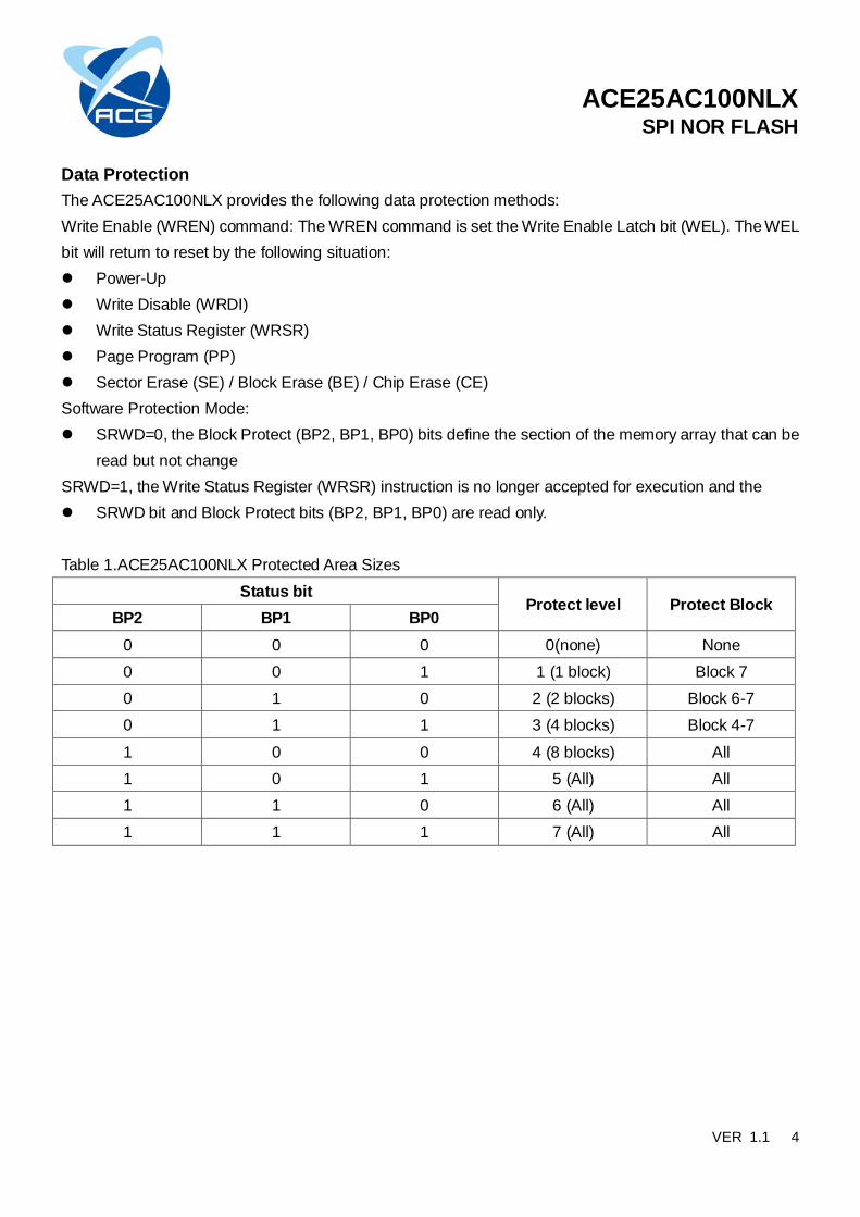
Data Protection The ACE25AC100NLX provides the following data protection methods: Write Enable (WREN) command: The WREN command is set the Write Enable Latch bit (WEL). The WEL bit will return to reset by the following situation: Power-Up Write Disable (WRDI) Write Status Register (WRSR) Page Program (PP) Sector Erase (SE) / Block Erase (BE) / Chip Erase (CE) Software Protection Mode: SRWD=0, the Block Protect (BP2, BP1, BP0) bits define the section of the memory array that can be
read but not change SRWD=1, the Write Status Register (WRSR) instruction is no longer accepted for execution and the SRWD bit and Block Protect bits (BP2, BP1, BP0) are read only. Table 1.ACE25AC100NLX Protected Area Sizes
The status and control bits of the Status Register are as follows: WIP bit. The Write In Progress (WIP) bit indicates whether the memory is busy in program/erase/write status register progress. When WIP bit sets to 1, the device is busy in program/erase/write status register progress. When WIP bit sets 0, the device is not in program, erase or write status register. WEL bit. The Write Enable Latch (WEL) bit indicates the status of the internal Write Enable Latch. When set to 1, the internal Write Enable Latch is set. When set to 0, the internal Write Enable Latch is reset and no Write Status Register, Program or Erase command is accepted. BP2, BP1, BP0 bits. The Block Protect (BP2, BP1, BP0) bits are non-volatile. They define the size of the area to be software protected against Program and Erase commands. These bits are written with the Write Status Register (WRSR) command. When the Block Protect (BP2, BP1, BP0) bits are set to 1, the relevant memory area (as defined in Table1) becomes protected against Page Program (PP), Sector Erase (SE) and Block Erase (BE) commands. Chip Erase command will be ignored if one or more of the Block Protect (BP2, BP1, BP0) bits are 1. SRWD bit. The Status Register Write Disable (SRWD) bit is a non-volatile One Time Program (OTP) bit in the status register that provide another software protection. Once it is set to 1, the Write Status Register (WRSR) instruction is no longer accepted and the SRWD bit and Block Protect bits (BP2, BP1, BP0) are read only.
SRWD Status register Memory
0 Status register can be written in (WEL bit is
set to "1") and the SRWD, BP2-BP0 bits can be changed
The protected area cannot be program or erase
1 The SRWD, BP2-BP0 of status register bits
cannot be changed The protected area cannot be program or erase
ACE25AC100NLX
SPI NOR FLASH
VER 1.1 6
Commands Description All commands, addresses and data are shifted in and out of the device, beginning with the most significant bit on the first rising edge of SCLK after CS# is driven low. Then, the one-byte command code must be shifted in to the device, most significant bit first on SI, each bit being latched on the rising edges of SCLK. See Table2, every command sequence starts with a one-byte command code. Depending on the command, this might be followed by address bytes, or by data bytes, or by both or none. CS# must be driven high after the last bit of the command sequence has been shifted in. For the command of Read, Fast Read, Read Status Register, and Read Device ID, the shifted-in command sequence is followed by a data-out sequence. CS# can be driven high after any bit of the data-out sequence is being shifted out. For the command of Page Program, Sector Erase, Block Erase, Chip Erase, Write Status Register, Write Enable, Write Disable, CS# must be driven high exactly at a byte boundary, otherwise the command is rejected. That is CS# must driven high when the number of clock pulses after CS# being driven low is an exact multiple of eight. For Page Program, if at any time the input byte is not a full byte, nothing will happen and WEL will not be reset. Table2. Commands
Command Name Byte1 Byte2 Byte3 Byte4 Byte5 Byte6 n-Bytes
Write Enable 06H
Write Disable 04H
Read Status Register 05H (S7-S0) (continuous)
Write Status Register 01H (S7-S0) (continuous)
Read Data 03H A23-A16 A15-A8 A7-A0 (D7-D0) (Next byte) (continuous)
Fast Read 0BH A23-A16 A15-A8 A7-A0 dummy (D7-D0) (continuous)
Page Program 02H A23-A16 A15-A8 A7-A0 (D7-D0) (Next byte)
Sector Erase 20H A23-A16 A15-A8 A7-A0
Block Erase D8H A23-A16 A15-A8 A7-A0
Chip Erase C7/60H
Manufacturer/Device
ID 90H dummy dummy 00H (MID7-MID0) (DID7-DID0) (continuous)
Read Identification 9FH (MID7-MID0) (JDID15-JDI
D8)
(JDID7-JDID
0) (continuous)
ACE25AC100NLX
SPI NOR FLASH
VER 1.1 7
ID Definitions
Operation Code M7-M0 ID15-ID8 ID7-ID0
9FH 0E 60 13
90H 0E 12
Write Enable (WREN) (06H) The Write Enable (WREN) command is for setting the Write Enable Latch (WEL) bit. The Write Enable Latch (WEL) bit must be set prior to every Page Program (PP), Sector Erase (SE), Block Erase (BE), Chip Erase (CE) and Write Status Register (WRSR) command. The Write Enable (WREN) command sequence: CS# goes low→Send Write Enable command→CS# goes high.
Write Disable (WRDI) (04H) The Write Disable command is for resetting the Write Enable Latch (WEL) bit. The Write Disable command sequence: CS# goes low →Send Write Disable command →CS# goes high. The WEL bit is
reset by following condition: Power-up and upon completion of the Write Status Register, Page Program, Sector Erase, Block Erase and Chip Erase commands.
Figure1. Write Enable Sequence Diagram
Figure2. Write Disable Sequence Diagram
ACE25AC100NLX
SPI NOR FLASH
VER 1.1 8
Read Status Register (RDSR) (05H) The Read Status Register (RDSR) command is for reading the Status Register. The Status Register may be read at any time, even while a Program, Erase or Write Status Register cycle is in progress. When one of these cycles is in progress, it is recommended to check the Write In Progress (WIP) bit before sending a new command to the device. It is also possible to read the Status Register continuously.
Write Status Register (WRSR) (01H) The Write Status Register (WRSR) command allows new values to be written to the Status Register. Before it can be accepted, a Write Enable (WREN) command must previously have been executed. After the Write Enable (WREN) command has been decoded and executed, the device sets the Write Enable Latch (WEL). The Write Status Register (WRSR) command has no effect on S6, S5, S1 and S0 of the Status Register. CS# must be driven high after the eighth bit of the data byte has been latched in. If not, the Write Status Register (WRSR) command is not executed. As soon as CS# is driven high, the self-timed Write Status Register cycle (whose duration is tW) is initiated. While the Write Status Register cycle is in progress, the Status Register may be read to check the value of the Write In Progress (WIP) bit. The Write In Progress (WIP) bit is 1 during the self-timed Write Status Register cycle, and is 0 when it is completed. When the cycle is completed, the Write Enable Latch (WEL) is reset. The Write Status Register (WRSR) command allows the user to change the values of the Block Protect (BP2, BP1, BP0) bits, to define the size of the area that is to be treated as read-only, as defined in Table1.1 and 1.2. The Status Register Write Disable (SRWD) bit is a non-volatile One Time Program(OTP) bit, the Write Status Register (WRSR) command allows the user to set the Status Register Write Disable (SRWD) bit to 1. The Status Register Write Disable (SRWD) bit allow the device to be put in another Software Protected Mode. Once the SRWD bit is set to 1, the Write Status Register (WRSR) command is not executed, and the SRWD bit and Block Protect bits (BP2, BP1, BP0) are read only.
Figure3. Read Status Register Sequence Diagram
Figure4. Write Status Register Sequence Diagram
ACE25AC100NLX
SPI NOR FLASH
VER 1.1 9
Read Data Bytes (READ) (03H) The Read Data Bytes (READ) command is followed by a 3-byte address (A23-A0), each bit being latched-in during the rising edge of SCLK. Then the memory content, at that address, is shifted out on SO, each bit being shifted out, at a Max frequency fR, during the falling edge of SCLK. The first byte addressed can be at any location. The address is automatically incremented to the next higher address after each byte of data is shifted out. Therefore, the whole memory can be read with a single Read Data Bytes (READ) command. During an Erase, Program or Write cycle, Read Data Byte (READ) command will be rejected without affecting the cycle in progress.
Read Data Bytes At Higher Speed (Fast Read) (0BH) The Read Data Bytes at Higher Speed (Fast Read) command is for quickly reading data out. It is followed by a 3-byte address (A23-A0) and a dummy byte, each bit being latched-in during the rising edge of SCLK. Then the memory content, at that address, is shifted out on SO, each bit being shifted out, at a Max frequency fC, during the falling edge of SCLK. The first byte address can be at any location. The address is automatically incremented to the next higher address after each byte of data is shifted out.
Figure5. Read Data Bytes Sequence Diagram
Figure6. Read Data Bytes at Higher Speed Sequence Diagram
ACE25AC100NLX
SPI NOR FLASH
VER 1.1 10
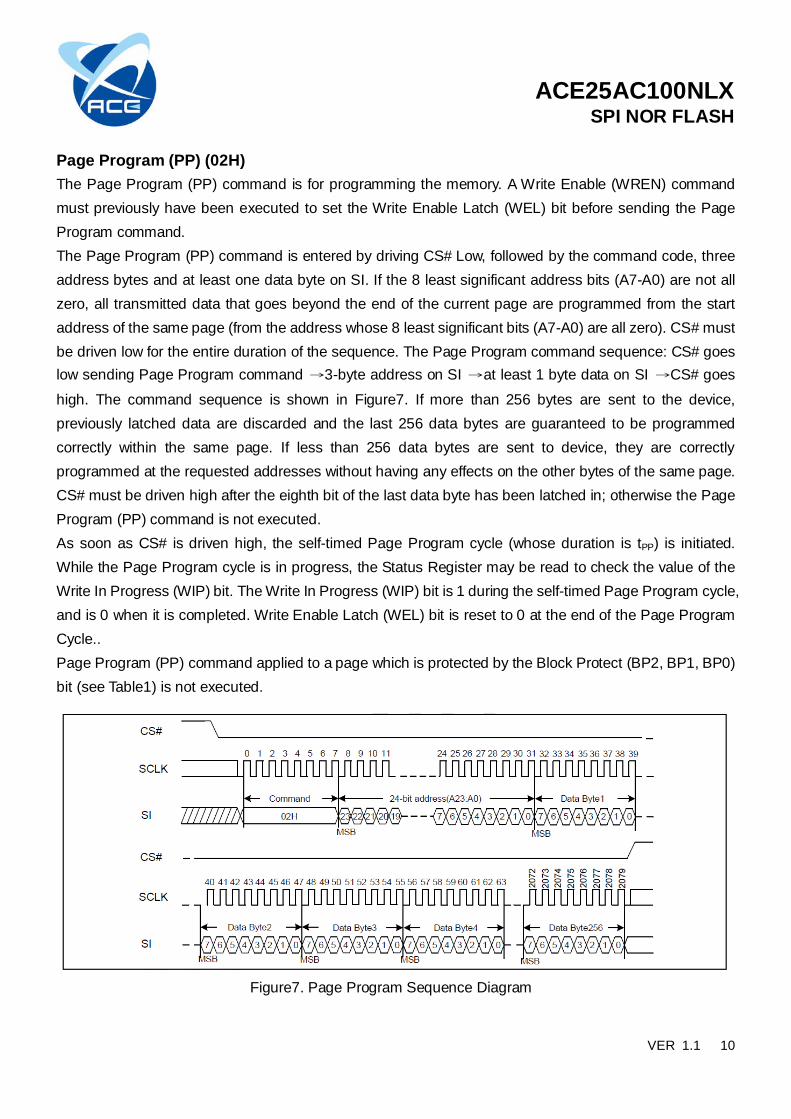
Page Program (PP) (02H) The Page Program (PP) command is for programming the memory. A Write Enable (WREN) command must previously have been executed to set the Write Enable Latch (WEL) bit before sending the Page Program command. The Page Program (PP) command is entered by driving CS# Low, followed by the command code, three address bytes and at least one data byte on SI. If the 8 least significant address bits (A7-A0) are not all zero, all transmitted data that goes beyond the end of the current page are programmed from the start address of the same page (from the address whose 8 least significant bits (A7-A0) are all zero). CS# must be driven low for the entire duration of the sequence. The Page Program command sequence: CS# goes low sending Page Program command →3-byte address on SI →at least 1 byte data on SI →CS# goes
high. The command sequence is shown in Figure7. If more than 256 bytes are sent to the device, previously latched data are discarded and the last 256 data bytes are guaranteed to be programmed correctly within the same page. If less than 256 data bytes are sent to device, they are correctly programmed at the requested addresses without having any effects on the other bytes of the same page. CS# must be driven high after the eighth bit of the last data byte has been latched in; otherwise the Page Program (PP) command is not executed. As soon as CS# is driven high, the self-timed Page Program cycle (whose duration is tPP) is initiated. While the Page Program cycle is in progress, the Status Register may be read to check the value of the Write In Progress (WIP) bit. The Write In Progress (WIP) bit is 1 during the self-timed Page Program cycle, and is 0 when it is completed. Write Enable Latch (WEL) bit is reset to 0 at the end of the Page Program Cycle.. Page Program (PP) command applied to a page which is protected by the Block Protect (BP2, BP1, BP0) bit (see Table1) is not executed.
Figure7. Page Program Sequence Diagram
ACE25AC100NLX
SPI NOR FLASH
VER 1.1 11
Sector Erase (SE) (20H) The Sector Erase (SE) command is for erasing the all data of the chosen sector. A Write Enable (WREN) command must previously have been executed to set the Write Enable Latch (WEL) bit. The Sector Erase (SE) command is entered by driving CS# low, followed by the command code, and 3-address byte on SI. Any address inside the sector is a valid address for the Sector Erase (SE) command. CS# must be driven low for the entire duration of the sequence. The Sector Erase command sequence: CS# goes low →sending Sector Erase command →3-byte address on SI →CS# goes high. The command sequence is shown in Figure8. CS# must be driven high after the eighth bit of the last address byte has been latched in; otherwise the Sector Erase (SE) command is not executed. As soon as CS# is driven high, the self-timed Sector Erase cycle (whose duration is tSE) is initiated. While the Sector Erase cycle is in progress, the Status Register may be read to check the value of the Write In Progress (WIP) bit. The Write In Progress (WIP) bit is 1 during the self-timed Sector Erase cycle, and is 0 when it is completed. Write Enable Latch (WEL) bit is reset to 0 at the end of the Sector Erase cycle. Sector Erase (SE) command applied to a sector which is protected by the Block Protect (BP2, BP1, BP0) bit (see Table1) is not executed.
Block Erase (BE) (D8H) The Block Erase (BE) command is for erasing the all data of the chosen block. A Write Enable (WREN) command must previously have been executed to set the Write Enable Latch (WEL) bit. The Block Erase (BE) command is entered by driving CS# low, followed by the command code, and three address bytes on SI. Any address inside the block is a valid address for the Block Erase (BE) command. CS# must be driven low for the entire duration of the sequence. The Block Erase command sequence: CS# goes low send Block Erase command 3-byte address on SI CS# goes h igh. The comman e driven high after the eighth bit of the last address byte has been latched in; otherwise the Block Erase (BE) command is not executed. As soon as CS# is driven high, the self-timed Block Erase cycle (whose duration is tBE) is initiated. While the Block Erase cycle is in progress, the Status Register may be read to check the value of the Write In Progress (WIP) bit. The Write In Progress (WIP) bit is 1 during the self-timed Block Erase cycle, and is 0 when it is completed. Write Enable Latch (WEL) bit is reset to 0 at the end of the Block Erase cycle. Block Erase (BE) commands applied to a block which is protected by the Block Protect (BP2, BP1, BP0) bits (see Table1) is not executed.
Figure8. Sector Erase Sequence Diagram
Figure9. Block Erase Sequence Diagram
ACE25AC100NLX
SPI NOR FLASH
VER 1.1 12
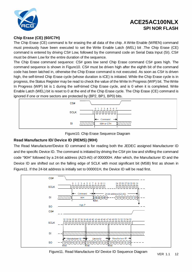
Chip Erase (CE) (60/C7H) The Chip Erase (CE) command is for erasing the all data of the chip. A Write Enable (WREN) command must previously have been executed to set the Write Enable Latch (WEL) bit .The Chip Erase (CE) command is entered by driving CS# Low, followed by the command code on Serial Data Input (SI). CS# must be driven Low for the entire duration of the sequence. The Chip Erase command sequence: CS# goes low send Chip Erase command CS# goes high. The command sequence is shown in Figure10. CS# must be driven high after the eighth bit of the command code has been latched in, otherwise the Chip Erase command is not executed. As soon as CS# is driven high, the self-timed Chip Erase cycle (whose duration is tCE) is initiated. While the Chip Erase cycle is in progress, the Status Register may be read to check the value of the Write In Progress (WIP) bit. The Write In Progress (WIP) bit is 1 during the self-timed Chip Erase cycle, and is 0 when it is completed. Write Enable Latch (WEL) bit is reset to 0 at the end of the Chip Erase cycle. The Chip Erase (CE) command is ignored if one or more sectors are protected by (BP2, BP1, BP0) bits.
Read Manufacture ID/ Device ID (REMS) (90H) The Read Manufacturer/Device ID command is for reading both the JEDEC assigned Manufacturer ID and the specific Device ID. The command is initiated by driving the CS# pin low and shifting the command code “90H” followed by a 24-bit address (A23-A0) of 000000H. After which, the Manufacturer ID and the Device ID are shifted out on the falling edge of SCLK with most significant bit (MSB) first as shown in Figure11. If the 24-bit address is initially set to 000001H, the Device ID will be read first.
Figure10. Chip Erase Sequence Diagram
Figure11. Read Manufacture ID/ Device ID Sequence Diagram
ACE25AC100NLX
SPI NOR FLASH
VER 1.1 13
Read Identification (RDID) (9FH) The Read Identification (RDID) command allows the 8-bit manufacturer identification to be read, followed by two bytes of device identification. The device identification indicates the memory type in the first byte, and the memory capacity of the device in the second byte. Any Read Identification (RDID) command while an Erase or Program cycle is in progress, is not decoded, and has no effect on the cycle that is in progress. The device is first selected by driving CS# to low. Then, the 8-bit command code for the command is shifted in. This is followed by the 24-bit device identification, stored in the memory, being shifted out on Serial Data Output, each bit being shifted out during the falling edge of Serial Clock. The command sequence is shown in Figure12. The Read Identification (RDID) command is terminated by driving CS# to high at any time during data output. After CS# is driven high, the device returns to Standby Mode and awaits for new command.
Figure12. Read Identification ID Sequence Diagram
ACE25AC100NLX
SPI NOR FLASH
VER 1.1 14
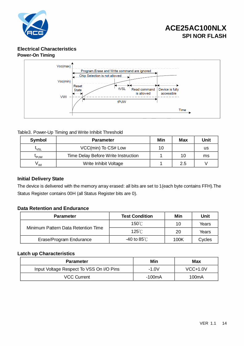
Electrical Characteristics Power-On Timing
Table3. Power-Up Timing and Write Inhibit Threshold
Symbol Parameter Min Max Unit tVSL VCC(min) To CS# Low 10 us tPUW Time Delay Before Write Instruction 1 10 ms VWI Write Inhibit Voltage 1 2.5 V
Initial Delivery State The device is delivered with the memory array erased: all bits are set to 1(each byte contains FFH).The Status Register contains 00H (all Status Register bits are 0). Data Retention and Endurance
Parameter Test Condition Min Unit
Minimum Pattern Data Retention Time 150℃ 10 Years 125℃ 20 Years
Erase/Program Endurance -40 to 85℃ 100K Cycles Latch up Characteristics
Parameter Min Max Input Voltage Respect To VSS On I/O Pins -1.0V VCC+1.0V
VCC Current -100mA 100mA
ACE25AC100NLX
SPI NOR FLASH
VER 1.1 15
Absolute Maximum Ratings
Parameter Value Unit Ambient Operating Temperature -40 to 85 ℃
Storage Temperature -65 to 150 ℃
Output Short Circuit Current 200 mA Applied Input/Output Voltage -0.5 to 4.0 V
VCC -0.5 to 4.0 V
Capacitance Measurement Condition
Symbol Parameter Min Typ Max Unit Conditions CIN Input Capacitance 6 pF VIN=0V
COUT Output Capacitance 8 pF VOUT=0V
CL Load Capacitance 30 pF
Input Rise And Fall time 5 ns
Input Pulse Voltage 0.1VCC to 0.8VCC V
Input Timing Reference Voltage 0.2VCC to 0.7VCC V
Output Timing Reference Voltage 0.5VCC V
Maximum Negative Overshoot Waveform
Maximum Positive Overshoot Waveform
Figure13. Input Test Waveform and Measurement Level
ACE25AC100NLX
SPI NOR FLASH
VER 1.1 16
DC Characteristics(T=-40℃~85℃,VCC=2.7~3.6V)
Symbol Parameter Test Condition Min. Typ Max. Unit
ILI Input Leakage Current ±2 μA
ILO Output Leakage Current ±2 μA
ICC1 Standby Current CS#=VCC
VIN=VCC or VSS 1 5 μA
ICC3 Operating Current(Read)
CLK=0.1VCC/0.9VCC at 120MHz for Fast Read
15 20 mA
CLK=0.1VCC/0.9VCC at 40MHz for Read
13 18
ICC4 Operating Current(PP) CS#=VCC 10 mA
ICC5 Operating Current(WRSR) CS#=VCC 10 mA
ICC6 Operating Current(SE) CS#=VCC 10 mA
ICC7 Operating Current(BE) CS#=VCC 10 mA
VIL Input Low Voltage -0.5 0.2VCC V
VIH Input High Voltage 0.7VCC VCC+0.4 V
VOL Output Low Voltage IOL=1.6mA 0.4 V
VOH Output High Voltage IOH=-100uA VCC-0.2 V
ACE25AC100NLX
SPI NOR FLASH
VER 1.1 17
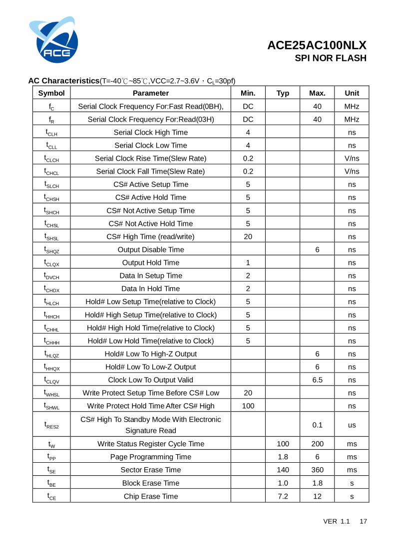
AC Characteristics(T=-40℃~85℃,VCC=2.7~3.6V,CL=30pf)
Symbol Parameter Min. Typ Max. Unit
fC Serial Clock Frequency For:Fast Read(0BH), DC 40 MHz
fR Serial Clock Frequency For:Read(03H) DC 40 MHz tCLH Serial Clock High Time 4 ns tCLL Serial Clock Low Time 4 ns
tCLCH Serial Clock Rise Time(Slew Rate) 0.2 V/ns tCHCL Serial Clock Fall Time(Slew Rate) 0.2 V/ns tSLCH CS# Active Setup Time 5 ns tCHSH CS# Active Hold Time 5 ns tSHCH CS# Not Active Setup Time 5 ns tCHSL CS# Not Active Hold Time 5 ns tSHSL CS# High Time (read/write) 20 ns tSHQZ Output Disable Time 6 ns tCLQX Output Hold Time 1 ns tDVCH Data In Setup Time 2 ns tCHDX Data In Hold Time 2 ns tHLCH Hold# Low Setup Time(relative to Clock) 5 ns tHHCH Hold# High Setup Time(relative to Clock) 5 ns tCHHL Hold# High Hold Time(relative to Clock) 5 ns tCHHH Hold# Low Hold Time(relative to Clock) 5 ns tHLQZ Hold# Low To High-Z Output 6 ns tHHQX Hold# Low To Low-Z Output 6 ns tCLQV Clock Low To Output Valid 6.5 ns tWHSL Write Protect Setup Time Before CS# Low 20 ns tSHWL Write Protect Hold Time After CS# High 100 ns
tRES2 CS# High To Standby Mode With Electronic
Signature Read 0.1 us
tW Write Status Register Cycle Time 100 200 ms tPP Page Programming Time 1.8 6 ms tSE Sector Erase Time 140 360 ms tBE Block Erase Time 1.0 1.8 s tCE Chip Erase Time 7.2 12 s
ACE25AC100NLX
SPI NOR FLASH
VER 1.1 18
Figure14. Serial Input Timing
Figure15. Output Timing
ACE25AC100NLX
SPI NOR FLASH
VER 1.1 19
Packaging information USON3*2-8
Symbol Dimensions In Millimeters Dimensions In Inches
Min Max Min Max
A 0.450 0.550 0.017 0.021 A1 0.000 0.050 0.000 0.002
b 0.180 0.300 0.007 0.039
b1 0.160REF 0.006REF
c 0.100 0.200 0.004 0.008
D 1.900 2.100 0.075 0.083
D2 1.400 1.600 0.055 0.062
e 0.500BSC 0.020BSC
Nd 1.500BSC 0.059BSC E 2.900 3.100 0.114 0.122
E2 1.500 1.700 0.059 0.067
L 0.300 0.500 0.012 0.020
h 0.200 0.300 0.066 0.12
ACE25AC100NLX
SPI NOR FLASH
VER 1.1 20
Notes ACE does not assume any responsibility for use as critical components in life support devices or systems without the express written approval of the president and general counsel of ACE Electronics Co., LTD. As sued herein: 1. Life support devices or systems are devices or systems which, (a) are intended for surgical implant
into the body, or (b) support or sustain life, and shoes failure to perform when properly used in accordance with instructions for use provided in the labeling, can be reasonably expected to result in a significant injury to the user.
2. A critical component is any component of a life support device or system whose failure to perform can be reasonably expected to cause the failure of the life support device or system, or to affect its safety or effectiveness.