Achieving low noise in scanning tunnelingspectroscopy Cite as: Rev. Sci. Instrum. 90, 101401 (2019); https://doi.org/10.1063/1.5111989Submitted: 31 May 2019 . Accepted: 09 September 2019 . Published Online: 02 October 2019
Jian-Feng Ge , Maoz Ovadia, and Jennifer E. Hoffman
COLLECTIONS
This paper was selected as Featured
ARTICLES YOU MAY BE INTERESTED IN
The qPlus sensor, a powerful core for the atomic force microscopeReview of Scientific Instruments 90, 011101 (2019); https://doi.org/10.1063/1.5052264
Design and analysis of the Tesla transformer with duplex secondary windingReview of Scientific Instruments 90, 106104 (2019); https://doi.org/10.1063/1.5123190
A high-pressure x-ray photoelectron spectroscopy instrument for studies of industriallyrelevant catalytic reactions at pressures of several barsReview of Scientific Instruments 90, 103102 (2019); https://doi.org/10.1063/1.5109321
ABSTRACTScanning tunneling microscopy/spectroscopy (STM/S) is a powerful experimental tool to understand the electronic structure of materi-als at the atomic scale, with energy resolution down to the microelectronvolt range. Such resolution requires a low-vibration laboratory,low-noise electronics, and a cryogenic environment. Here, we present a thorough enumeration and analysis of various noise sources andtheir contributions to the noise floor of STM/S measurements. We provide a comprehensive recipe and an interactive python notebookto input and evaluate noise data, and to formulate a custom step-by-step approach for optimizing the signal-to-noise ratio in STM/Smeasurements.Published under license by AIP Publishing. https://doi.org/10.1063/1.5111989., s
I. INTRODUCTION
Scanning tunneling microscopy (STM) measures the net elec-tric current I across a voltage-biased tunnel junction by bringing asharp metallic tip into atomic-scale proximity with a sample. In thesimplest mode of STM imaging, a feedback loop is used to main-tain a constant tunneling current, by tracing out the atomic-scaletopographical contours of the sample surface. The tunneling cur-rent is typically proportional to the energy-integrated density ofstates (DOS) of the sample surface, and thus scanning tunnelingspectroscopy (STS) was suggested1 and carried out2 soon after theinvention of STM. By STS, one can acquire the differential conduc-tance g(V) = dI/dV as the sample energy probed (eV) is tuned bybias voltage (V), with resolution reaching the microvolt range. Aspatial map of g(r, V) can be generated by raster scanning (x, y) onthe surface and sweeping V at each pixel.
Momentum resolution can be achieved by Fourier transform(FT) of a g(r, V) map where surface imperfections cause quasipar-ticle scattering, yielding DOS as a function of in-plane momentumand energy g(q, V).3,4 Here, the momentum q is the difference ofinitial and final momenta ki and kf of a scattered quasiparticle. Thistechnique, referred to as quasiparticle interference (QPI) imaging,enables observation of the local electronic band structure of the crys-tal surface. QPI imaging has been widely implemented in condensed
matter physics research, including high-temperature superconduc-tivity,5–8 heavy fermion compounds,9–11 graphene,12 and topologi-cal materials.13–16 While direct observation of the surface electronicband structure is achievable by angle-resolved photoemission spec-troscopy (ARPES), it is typically limited to occupied states (unlessa delicate optical pump-probe setup is implemented17–19) and itsspatial resolution is restricted by its optical wavelength (a few hun-dred nanometers). As a consequence, ARPES may inadvertentlyaverage multiple band structure signals from different domains orphases. On the other hand, QPI imaging can achieve spatial res-olution down to the Fermi wavelength (typically a few nanome-ters) and can access unoccupied states simply by applying a posi-tive sample bias voltage. Moreover, QPI can be used to image bandstructure dependence on the magnetic field, which is impossiblewith ARPES.
Time is the major limiting factor for high-resolution QPI imag-ing. First, a large real space area is required to maximize the QPImomentum resolution. Momentum resolution in ARPES is on theorder of 10−2 Å−1,20,21 which equates to around 70 nm in real space.Second, high spatial resolution is required to compensate for theinevitable thermal drift caused by minute, time-dependent tempera-ture gradients between tip and sample. Thermal drift leads to offsetsin the spatial registration of individual spectra, which degrades themomentum resolution. If the drift is less than ∼1 Å/h and the image
is acquired with atomic resolution in real space, then the Braggpeaks in the FT can serve as an exact length reference to correct thein-plane drift down to the picometer scale.22,23
As a concrete example of QPI parameters, in order to achievea momentum resolution of 10−2 Å−1, an area as large as ∼70 nm× 70 nm is necessary. Additionally, a grid with 256 × 256 pointsis desired to obtain atomic resolution in the 70 nm × 70 nm area(in-plane lattice constant is 3–6 Å for common materials) suchthat the whole Brillouin zone can be captured in the g(q, V) map.To obtain 1 meV energy resolution in a 0.1 eV energy windowthen requires 256 × 256 × 100 = 6.55 × 10⁶ distinct measure-ments. As the holding time of a cryostat at base temperature typ-ically varies from 50–200 h, this allows only 25–100 ms to ramp,settle, and integrate for each measurement. Therefore, it is crucialto improve the signal-to-noise ratio (SNR), defined as the ratio ofthe mean value to the standard deviation of the measured signal ofinterest X(t),
SNR =Xs
√1t0 ∫
t00 [X(t) − Xs]2dt
, (1)
where t0 is the duration of the measurement and Xs =1t0∫
t00 X(t)dt is
the mean value of the measured signal as t0 →∞. The denominatorin Eq. (1) is the square root of the noise power,
Pnoise =1t0∫
t0
0[x(t)]2dt, (2)
where x(t) = X(t) − Xs is the noise.24 Generally, if the SNR of a singlespectrum increases by a factor of 2, then it takes approximately 1/
√2
of the measurement time to achieve the same result. With this timesaving, one could increase the energy window, increase the energyresolution, or increase the momentum resolution by expanding thescan area if surface conditions allow.
The remainder of this review is organized as follows: InSec. II, we establish a general formula for the SNR of STSusing the homodyne (“lock-in”) method to measure differen-tial conductance. We also discuss the choice of the low-pass fil-ters (LPFs) for lock-in detection. In Sec. III, we introduce a toymodel for noise and then demonstrate its application using ourSTM data. In Sec. IV, we discuss in detail three fundamentalnoise sources (transimpedance preamplifier noise, tunnel junc-tion noise, and tip-sample distance modulation noise) and solu-tions to minimize them. Finally, in Sec. V, we summarize andgive a practical step-by-step algorithm, supported by our open-source code, at https://github.com/Let0n/achievinglownoiseinsts, tooptimize the SNR in its own STS and QPI measurements. Thereader is encouraged to follow all analyses using the comprehen-sive example code provided25 and to input his or her own noisedata in order to attain specific recommendations to optimize anSTM system.
II. SIGNAL-TO-NOISE RATIO IN SCANNINGTUNNELING SPECTROSCOPY
There are two methods to perform STS, namely, the DCmethod and the lock-in method. In the DC method, bias voltageVdc is swept in the energy range of interest and DC current Idc is
recorded at each point. Then, first-order numerical differentiation isapplied to the Idc(V) curve to obtain g(V). In the lock-in method,an AC voltage excitation with a small amplitude Vac at some fre-quency f 0 is added to a DC voltage sweep, then the AC currentamplitude Iac at the same frequency f 0 is measured by a lock-inamplifier. Differential conductance g(V) is then a simple divisionof Iac/Vac.
Because STM works at an ultralow current range on the orderof 10−12 A, we read out tunneling current with the aid of a tran-simpedance amplifier (TIA) (often referred to as a “preamplifier”),which converts current to voltage. All the information, includingboth signal and noise, is contained in the output. To discern dif-ferent noise components, it is more constructive to look at the fre-quency domain of the output (using a spectrum analyzer) than timedomain (using an oscilloscope). Therefore, we rewrite Eq. (1) in thefrequency domain,
SNR =⎡⎢⎢⎢⎢⎣
X2s
∫
∞
−∞
∣x( f )∣2df
⎤⎥⎥⎥⎥⎦
1/2
, (3)
where the Fourier transform takes the form of x( f ) = 1√
t0∫
t00 e−2πjft
x(t)dt.26 We use j as the imaginary unit to distinguish it from thenoise current i introduced later.
Figure 1 shows a schematic of the typical noise power spec-tral density (PSD) of the STM tunneling current measured by apreamplifier, which is composed of three parts:
1. Flicker noise dominates from DC up to a corner frequencyf F. The PSD of flicker noise can be expressed27 as KFI2/f,where KF is an empirical coefficient, so the flicker noise isalso known as “1/f noise.” The origin of flicker noise hasbeen attributed to mobility fluctuations or charge trapping inelectronic devices.27,28
2. The middle-frequency range extending from f F to the band-width of the preamplifier is typically relatively flat and pri-marily from the Johnson-Nyquist current noise. We willdiscuss the composition of preamplifier noise current PSDSaa( f ) in Sec. IV A. The corner frequency of flicker noisef F varies with tunneling current and can be determined byKFI2/f F = Saa( f F).
FIG. 1. An illustrative example of typical noise current PSD of a STM tunnel junc-tion. The corner frequency of Flicker noise is labeled f F. The bandwidth of thepreamplifier, f amp, is 4 kHz in this example.
3. A preamplifier has a second- or higher-order low-pass filter(LPF) with a cutoff frequency f amp, so noise at frequenciesabove f amp is heavily suppressed. The LPF of the preamplifieracts on the signal as well, so the signal is also suppressed abovef amp.
From Fig. 1, we can see that the noise spectral density is lowerin the middle frequency range, where the signal is not yet atten-uated by the cutoff frequency f amp. Generally, it is more advanta-geous to use the lock-in method with a frequency in this middle-frequency range than the DC method to optimize the SNR whenflicker noise dominates in the low frequency range.29–31 Specif-ically, the lock-in method will give a higher SNR than the DCmethod when flicker noise power PF is larger than preamplifier noisepower Pamp,
PF = ∫
fF
fmeas
KFI2
fdf > Pamp = ∫
famp
0Saa( f )df , (4)
where Saa( f ) will be quantified in Eq. (52) and the lower boundfmeas ∼ (2πtmeas)
−1 is the frequency associated with the time scale ofa single measurement tmeas. In practice, one can measure the currentnoise PSD with sufficient frequency resolution to fit the values ofKF and f F, then compare flicker noise power with preamplifier noisepower to determine which method should be used in spectroscopy.Except in rare cases, flicker noise dominates, so hereafter we willfocus on the more advantageous lock-in method for spectroscopicmeasurements.
A. Tunneling spectroscopy with a lock-in amplifierHomodyne detection is commonly carried out by a lock-in
amplifier. A lock-in amplifier performs a multiplication (demod-ulation) of its input (transimpedance-amplified tunneling current)with the reference signal (bias modulation) and then applies a low-pass filter to the product to recover the signal at the modulationfrequency. As shown in the circuit diagram in Fig. 2(a), a spectro-scopic measurement is performed by applying a DC voltage biasVdc and AC voltage modulation Vac to the tunnel junction at fre-quency f 0. For a tunnel junction with a current-to-voltage relationI(V), at small enough Vac, a Taylor expansion gives the resultingcurrent,
where the last two terms are additive noise due to the current fluc-tuations in the tunnel junction ij(t) and the noise of the preamplifieria(t). In Eq. (5), the first three terms I(Vdc), g(Vdc), and ij(t) aredefined at the average tip-to-sample distance z0. Tunneling currentis actually proportional to e−κz(t ), where κ−1 is the current decaylength, so we need to multiply the first three terms in Eq. (5) bya factor of e−κz(t ). If we write z(t) = z0 − zn(t), where zn(t) is thedisturbance in the tip-sample distance, then we can approximateEq. (5) to first order, assuming κzn ≪ 1 and neglecting second- andhigher-order terms
FIG. 2. Tunneling spectroscopy with a lock-in amplifier. (a) A circuit diagram ofa spectroscopic measurement with a modulation frequency f 0. Iac,x and Iac,y aretwo orthogonal components of the demodulation signal I2
ac = I2ac,x + I2
ac,y. (b) Anexample I(V) curve (black) showing modulation and demodulation in the lock-inmethod. At each point of the curve (black) that arises from sample characteristics,a bias modulation (red) with a peak amplitude of Vac is superimposed on a DCbias voltage Vdc. The resulting current (blue) has a DC value of Idc and an ACcomponent with a peak amplitude of Iac. The derived g(V) spectrum is shown inFig. 3(a).
Note that ζ(t) is a dimensionless function that quantifies the modu-lation of the instantaneous tunneling current by fluctuations in thetip-sample distance z(t). For example, if the current at z = z0 is equalto I0, then I(t) = I0[1 + ζ(t)].
The lock-in amplifier first removes the DC component inEq. (7) via a high-pass filter (which usually has a cutoff frequencyless than 1 Hz), then the remaining AC signal is demodulated bymultiplying by cos(2πf 0t).32 The resulting demodulated signal33
[Fig. 2(a)] is proportional to the sum of the “noise-free” signalXs = Iac and the noise current x(t) = i(t),
We then transform Eq. (10) to the frequency domain to analyzenoise contributions. The Fourier transform of a product of twofunctions is equal to the convolution of their Fourier transforms.The Fourier transform of the cosine function is a pair of Dirac δ-functions, so their convolution with other functions is especiallysimple
= Iacζ( f) + Idc[ζ( f − f0) + ζ( f + f0)] + [ia( f − f0) + ia( f + f0)]
+ [ij( f − f0) + ij( f + f0)] + 12 Iac[ζ( f − 2f0) + ζ( f + 2f0)]
+ 12 Iac[δ( f − 2f0) + δ( f + 2f0)]. (11)
The noise PSD is given by
Sii( f ) = i( f )i∗( f ), (12)
where i∗( f ) denotes the complex conjugate of i( f ). The noise PSDcontains
1. autocorrelation terms such as ζ( f )ζ∗( f ) and ζ( f − 2f 0)ζ∗( f − 2f 0),
2. cross-correlation terms between two different functions, suchas ζ( f − f0)i∗a ( f − f0) and ζ( f − 2f 0)δ∗( f − 2f 0),
3. cross-correlation terms between the same function with differ-ent frequency shifts, such as ζ( f − f 0)ζ∗( f − 2f 0).
The cross correlation between two different random functions, whenaveraged across multiple realizations, is zero if their respective pro-cesses are uncorrelated. The terms ia, ij, and ζ are completely uncor-related with each other, so their cross-correlation terms can bedropped. Similarly, the correlation between two frequency-shiftedversions of ia or ij, dominated by flicker noise or the Johnson-Nyquist current noise, is zero. However, it is not clear if terms suchas ζ( f − f 0)ζ∗( f − 2f 0) can be dropped because the physical compo-nents that cause the vibration noise may have harmonics that lead toa nonzero cross correlation between frequency-shifted versions of ζ.In what follows we assume that all cross-correlation terms are negli-gible. It is a good approximation as long as we choose a modulationfrequency f 0 such that both f 0 and 2f 0 are away from mechanicalor electrical resonances of the system and environment [so cross-correlation terms such as ζ( f − 2f 0)δ∗( f − 2f 0) vanish]. We alsoshow an example in Fig. 24 in the Appendix that the estimated
lock-in demodulation current PSD under this approximation stillagrees quite well with the measured result.
Defining
Sζζ( f ) = ζ( f )ζ∗( f ), (13a)
Saa( f ) = ia( f )i∗a ( f ), (13b)
Sjj( f ) = ij( f )i∗j ( f ), (13c)
we can write the total PSD as the sum of all PSDs of the individualterms of i( f ),34
Sii( f ) = I2acSζζ( f ) + I2
dc[Sζζ( f − f0) + Sζζ( f + f0)]
+ [Saa( f − f0) + Saa( f + f0)] + [Sjj( f − f0) + Sjj( f + f0)]
+ 14 I2
ac[Sζζ( f − 2f0) + Sζζ( f + 2f0)]
+ 14 I2
ac[δ( f − 2f0) + δ( f + 2f0)]. (14)
To make this notation more compact, we define the modulated noisePSDs
Sζζ,f0 ≡12 [Sζζ( f − f0) + Sζζ( f + f0)], (15a)
Saa,f0 ≡12 [Saa( f − f0) + Saa( f + f0)], (15b)
Sjj,f0 ≡12 [Sjj( f − f0) + Sjj( f + f0)], (15c)
Sδδ,2f0 ≡12 [δ( f − 2f0) + δ( f + 2f0)], (15d)
so that the total current PSD of the demodulated signal becomes
Sii = I2acSζζ,0 + 2I2
dcSζζ,f0 + 2Saa,f0 + 2Sjj,f0+ 1
2 I2acSζζ,2f0 + 1
2 I2acSδδ,2f0 ,
(16)
which can be compared with the signal power I2ac.
During a spectroscopic measurement, Iac is generally not a con-stant but is typically bounded, whereas Idc is assumed to be a mono-tonic function of Vdc that typically reaches values much larger thanIac. It is interesting, therefore, to note the dependence of the differentnoise contributions on the ratio Idc/Iac,
Sii/I2ac = Sζζ,0 +
Sζζ,2f0
2+
Sδδ,2f0
2+
2Saa,f0
I2ac
+2Sjj,f0
I2ac
+ 2Sζζ,f0(Idc
Iac)
2
= Sζζ,0 +Sζζ,2f0
2+
Sδδ,2f0
2+
2Saa,f0
I2ac
+2kBTRjI2
ac
+2eIac(
Idc
Iac) + 2Sζζ,f0(
Idc
Iac)
2, (17)
where we have approximated the junction noise Sjj,f0 as the sumof the Johnson-Nyquist current noise and shot noise components(we will discuss them in detail in Sec. IV B). Apparently, there areterms independent of Idc/Iac, one term linear in Idc/Iac, and one termquadratic in Idc/Iac that gradually dominates the noise spectrum asthe bias voltage is increased.
In order to calculate the output noise power Pnoise from thedemodulated noise current PSD Sii, we must take into account the
output LPF of the lock-in amplifier. The lock-in amplifier LPF has atransfer function H( f ), giving
Pnoise = ∫
∞
−∞
[H( f )i( f )][H( f )i( f )]∗df
= ∫
∞
−∞
Sii( f )∣H( f )∣2df . (18)
We define four dimensionless specific noise power
pζζ,0 = ∫
∞
−∞
Sζζ,0∣H( f )∣2df , (19a)
pζζ,f0 = ∫
∞
−∞
Sζζ,f0 ∣H( f )∣2df , (19b)
pζζ,2f0 = ∫
∞
−∞
Sζζ,2f0 ∣H( f )∣2df , (19c)
pδδ,2f0 = ∫
∞
−∞
Sδδ,2f0 ∣H( f )∣2df = ∣H(2f0)∣2, (19d)
and two current noise power
Paa,f0 = ∫
∞
−∞
Saa,f0 ∣H( f )∣2df , (20a)
Pjj = ∫
∞
−∞
Sjj∣H( f )∣2df = 2SjjBN. (20b)
We will discuss the frequency dependence of Saa,f0 in Sec. IV A, whilein Eq. (20b), we use the fact that Sjj is frequency independent (seeSec. IV B), and BN = ∫
∞
0 ∣H( f )∣2df is the equivalent noise bandwidth(ENBW) of the LPF of the lock-in amplifier assuming a passbandgain of 1. We can finally obtain the SNR as
SNR =Iac√
Pnoise=
⎡⎢⎢⎢⎢⎣
pζζ,0 + 2(Idc
Iac)
2pζζ,f0 +
2Paa,f0
I2ac
+2Pjj
I2ac
+12
pζζ,2f0 +12∣H(2f0)∣
2⎤⎥⎥⎥⎥⎦
−1/2
. (21)
Commonly, the SNR is expressed in decibels
SNR[dB] = 20 log10(Iac√
Pnoise)
= −10 log10[pζζ,0 + 2(I2
dc
I2ac)pζζ,f0 +
2Paa,f0
I2ac
+2Pjj
I2ac
+12
pζζ,2f0 +12∣H(2f0)∣
2]. (22)
For example, an SNR of 40 dB means that the root-mean-square(rms) noise amplitude is 1% of the signal.
Equation (22) gives a mathematical expression to calculate theSNR from specific noise sources. Practically, the SNR can also beestimated as the mean value of g(V) divided by the standard devi-ation of g(V) from multiple spectra because g × Vac = Iac, andthe standard deviation of Iac is equal to
√Pnoise (square root of
frequency-integrated PSD). We show in Fig. 3 the relation betweenSNR in direct measured g(V) spectra and SNR derived from currentnoise PSD out of the lock-in amplifier [i.e., from Eq. (22)]. The fluc-tuations in single spectra (red) in Fig. 3(a) indicate visually the rmsnoise amplitude compared to the signal (the black average curve). Toclarify the simple relationship between Iac and g, we note the mea-sured Iac = 13.8 pA at Vdc = 0.40 V yields g(0.4 V) = 2.76 nA/V. AtVdc = 0.40 V, g = 2.771 ± 0.065 nA/V, and thus the SNR estimatedfrom 100 bias spectra in Fig. 3(a) is 32.6 dB. On the other hand, inte-grating Fig. 3(c) from 5 Hz to 5 kHz gives
√Pnoise of 0.38 pA, which
yields a SNR of 31.9 dB using Eq. (22). Therefore, the estimation ofthe SNR from multiple spectra taken at identical conditions agreeswell with the SNR derived from Eq. (22). We also note that the stan-dard deviation of g(V) increases with increasing |Idc| in Fig. 3(b),indicating a smaller SNR with a higher tunneling current.
We pause at this point to inspect the different factors thatinfluence the SNR
1. The LPF of the lock-in amplifier with the transfer function|H( f )| is selected by the experimenter. We will discuss thechoice of LPF in Sec. II B.
FIG. 3. Illustration of SNR in terms of bias spectroscopy and frequency spectroscopy. (a) Average bias spectrum g(V) (black) of 100 spectra [20 randomly selected singlespectra are shown (red)] taken with the same setup conditions of Vdc = 0.40 V, Idc = 1.0 nA measured on a cleaved semimetal CeBi surface at 4 K. A bias modulation withfrequency f 0 = 1.17 kHz and Vac = 5 mV was applied. Simutanously taken Idc(V) (blue) is shown to convert from Vdc to Idc. (b) Standard deviation of differential conductanceσ(g) in (a) shows an increasing trend with increasing |Idc|. (c) Current power spectral density of the lock-in output Sii |H(f )|2 as a function of frequency. The frequency spectrumwas measured with the same setup conditions Vdc = 0.40 V, Idc = 1.0 nA immediately before the bias spectroscopic measurement in (a), with the same bias modulationapplied. A boxcar (“synchronous”) filter at settling time ts = (2πf0)
−1 and then a second-order RC filter with ts = 10 ms were applied for both measurements in (a) and (b).The choice of low-pass filters will be discussed in Sec. II B.
2. Idc is determined by the sample properties, DC bias volt-age Vdc, and average tip-sample separation z0. Within a fewconstraints such as the current resolution and limits of thepreamplifier, the experimenter can select any z0.
3. Iac is determined by the sample properties, voltage modulationVac, and the junction impedance dV/dI
4. Vac is selected by the user and determines the energy reso-lution of the measurement when thermal broadening can beneglected, i.e., when eVac ≫ 2kBT j.35
5. Saa is determined by the preamplifier noise and may dependon the input impedance (including tunnel junction and cableimpedance) dV/dI. We will discuss Saa in Sec. IV A.
6. Sjj is composed of the junction Johnson-Nyquist current noiseproportional to junction temperature, and shot noise propor-tional to Idc. We will discuss Sjj in Sec. IV B.
7. Sζζ is determined by environmental vibrations and STM stiff-ness, by scan voltage noise and scanner response, and by theelectronic properties of the tip and sample that determine κ.We will discuss Sζζ in Sec. IV C.
The SNR may vary by over 10 dB at different Idc values within asingle spectroscopic measurement, as exemplified in Fig. 16. In orderto optimize the efficiency in a spectroscopic measurement, we cankeep the SNR approximately constant over the range of bias voltageeither by increasing the number of averages N(V) with increasing|V|, which increases the SNR by 10 log10 N dB, or by adjusting H( f )as a function of Vdc as shown in Sec. III A.
To give a clear view of how each term in Eq. (21) contributesto the SNR, Fig. 4 illustrates the noise flow toward the output of
the lock-in amplifier. The prime feature of the noise flow is thatthe noise experiences two convolution operations (labeled by redasterisks in Fig. 4) in the frequency domain: the first one betweendimensionless ζ(t) and current (both signal and noise) before enter-ing preamplifier input and the second one between the outputof the preamplifier and the reference signal in the lock-in ampli-fier. The consequence of the convolution operations is exhibitedin the terms involving the specific noise power of ζ such as pζζ,f0
in Eq. (22).
B. Choice of the low-pass filterfor the lock-in amplifier
We will first discuss the choice of LPF for the lock-in ampli-fier since it is flexible to control. After the demodulation process inthe lock-in amplifier [Eq. (9)], the signal Iac to be measured at theoutput of the lock-in is the DC component. Even without externalnoise sources ζ, ij, ia adding to the input of the lock-in amplifier,the demodulation also generates a 2f 0 component at the output withthe same amplitude as the signal Iac, as shown in Eq. (10). This 2f 0component, along with interfering noise at other frequencies, mustbe filtered out to obtain the desired DC component Iac. In orderto select an optimal LPF for the lock-in amplifier, one must con-sider the following: (1) the filter frequency response |H( f )|2 andits equivalent noise bandwidth BN. The smaller the BN, the lowerthe output noise. (2) The filter step response or more specificallyits settling time. The settling time determines how long one mustwait after setting up the measurement parameters before a validvalue appears at the output. These two factors are inversely related:
FIG. 4. The flowchart of signal and noise in the frequency domain in spectroscopic measurements with a lock-in amplifier. Voltage noise, current noise, and Z noise aredenoted by vn, i, and zn, respectively, while “env” is short for the environment. DAC stands for digital-to-analog converter. HVA stands for high voltage amplifier. EMI standsfor electromagnetic interference. AHVA and ATIA denote the gains of the HVA and preamplifier. dpiezo is the piezoelectric coefficient (in the unit of m/V) of the z piezo scanner.K is the mechanical transfer function of the full STM system from external vibrations to the tip-sample distance. The plus operation means rms sum (the powers rather thanthe amplitudes are additive), while the asterisk operation means convolution. ∫df is the integration to obtain the final results. The subscripts x and y are two orthogonalcomponents of the primitive output of the lock-in amplifier, which are used to derive Iac after adjusting the lock-in phase to remove the out-of-phase current that arises fromcapacitive coupling rather than tunneling.
a filter with small BN will result in lower noise but will have along settling time. A filter with a short settling time will have alarge BN.36
In the following, we compare two types of LPFs commonlyused in lock-in detection. We use a continuous-time approximation,despite the fact that most lock-in amplifiers today measure digitally.This approximation is valid when the sampling frequency is muchhigher than the modulation frequency used.
1. nth-order RC filterThis type of filter is described by a time constant τ and an order
n, which is equal to the number of cascaded first-order RC filters.The frequency response function of the filter is
H( f ) = (1
1 + j2πf τ)
n
. (23)
This function can be integrated to obtain the noise bandwidth BN,
BN =1
2πτ ∫∞
0(
11 + x2 )
ndx =
14√πτ
Γ(n − 12)
Γ(n), (24)
where Γ(n) is the Gamma function. This filter’s time-domainresponse to a unit step function is described by the followingequation:37
y(t) = ∫∞
−∞
u(t)h(t − t′)dt′ = 1 − e−t/τn−1
∑l=0
1l!(
tτ)
l, (25)
where u(t) is the unit step function and h(t) is the impulse responseof the filter [inverse Laplace transform of Eq. (23)]. We define thesettling time ts by demanding that the filter output is within 0.1% ofits asymptotic value, and therefore
1/1000 = e−ts/τn−1
∑l=0
1l!(
ts
τ)
l. (26)
Equation (26) can be solved easily for n = 1 but requires a numericalsolution for higher n. We show in Fig. 5 both the step response func-tion y(t) and the filter response function |H( f )|2 of the RC filter withan order ranging from 1 to 8 for an equal settling time of 10 ms. Thereader can play with the parameter τ in our code25 to determine thesettling time when an RC filter is used for the lock-in amplifier in aspectroscopic measurement. For an equal time constant [Fig. 5(a)],a higher order RC filter requires more time to settle after encoun-tering a step change in voltage during a spectroscopic measurement.On the other hand, a higher order RC filter has a lower noise band-width for an equal settling time [Fig. 5(b)]. The filter “efficiency” canbe determined by the time-bandwidth product tsBN, with a lowerproduct being better. Table I shows for different order n, the noisebandwidth BN, the settling time ts, the efficiency tsBN, and the fil-ter attenuation |H( f )|2 at the high frequency limit, for a given timeconstant. It also suggests that it is preferable to select a filter of ordern = 4 or higher.
2. Boxcar filter (“synchronous filter”)For the boxcar filter, the averaging time defines the settling time
ts = tavg. The filter has a frequency response of
H( f ) =sin(πtavg f )
πtavg f. (27)
FIG. 5. Response characteristics of nth-order RC filter with different n. (a) Time-domain step response y(t) for different n with an equal time constant τ = 1 ms.The black dashed line presents an ideal unit step response as a reference. (b)Frequency-domain response function |H(f )|2 for different n with an equal settlingtime ts = 10 ms defined in Eq. (26).
Again, we perform an integration to determine the noise bandwidthof this filter
BN = ∫
∞
0[
sin(πtavg f )πtavg f
]
2
df =1
2tavg. (28)
TABLE I. Noise bandwidth BN, settling time ts, time-bandwidth product tsBN, andfilter response function for RC filters with different order n, for a given filter timeconstant τ.
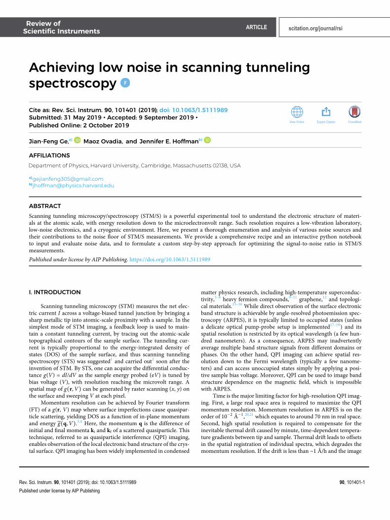
FIG. 6. Comparison of response function |H(f )|2 between a boxcar filter and a nth-order RC filter, with an equal settling time ts = 10 ms. The boxcar filter has anaveraging time tavg of 10 ms, while the RC filter has a time constant τ of 0.763 ms.
The time-bandwidth product for this filter is therefore
tsBN =12
, (29)
which is lower than any RC filter. If the goal is to attain the low-est possible noise bandwidth within a given measuring time, thenthe boxcar filter is preferred. We give an example in Fig. 6, showingthe comparison of response functions between a boxcar filter and a4th-order RC filter with the same settling time of 10 ms. The −3 dBbandwidth of the boxcar filter is 32.0 Hz, which is lower than thatof the 4th-order RC filter, 62.4 Hz. We note that the response func-tion of the boxcar filter has moderate high frequency “lobes,” whichshould be taken into account in lock-in measurements, as shown inFig. 10.
III. ANALYZING NOISE IN AN ACTUAL INSTRUMENTA. Toy model
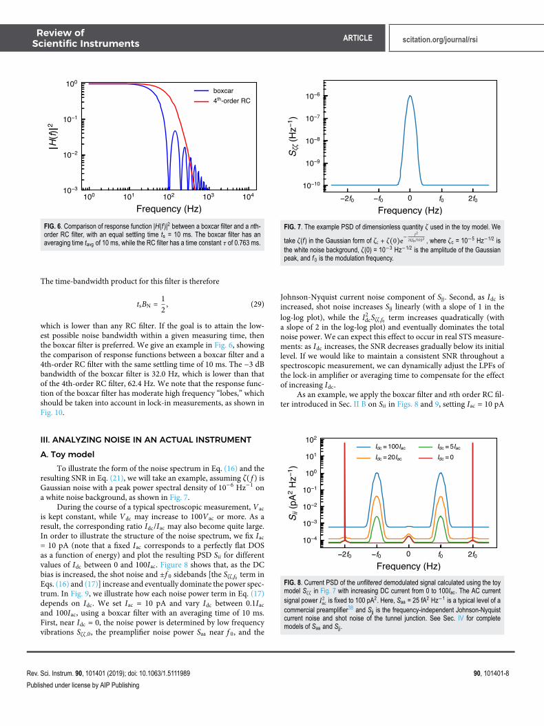
To illustrate the form of the noise spectrum in Eq. (16) and theresulting SNR in Eq. (21), we will take an example, assuming ζ( f ) isGaussian noise with a peak power spectral density of 10−6 Hz−1 ona white noise background, as shown in Fig. 7.
During the course of a typical spectroscopic measurement, Vacis kept constant, while Vdc may increase to 100Vac or more. As aresult, the corresponding ratio Idc/Iac may also become quite large.In order to illustrate the structure of the noise spectrum, we fix Iac= 10 pA (note that a fixed Iac corresponds to a perfectly flat DOSas a function of energy) and plot the resulting PSD Sii for differentvalues of Idc between 0 and 100Iac. Figure 8 shows that, as the DCbias is increased, the shot noise and ±f 0 sidebands [the Sζζ,f0 term inEqs. (16) and (17)] increase and eventually dominate the power spec-trum. In Fig. 9, we illustrate how each noise power term in Eq. (17)depends on Idc. We set Iac = 10 pA and vary Idc between 0.1Iacand 100Iac, using a boxcar filter with an averaging time of 10 ms.First, near Idc = 0, the noise power is determined by low frequencyvibrations Sζζ ,0, the preamplifier noise power Saa near f 0, and the
FIG. 7. The example PSD of dimensionless quantity ζ used in the toy model. We
take ζ(f ) in the Gaussian form of ζc + ζ(0)e−f 2
2(f0/10)2 , where ζc = 10−5 Hz−1/2 isthe white noise background, ζ(0) = 10−3 Hz−1/2 is the amplitude of the Gaussianpeak, and f 0 is the modulation frequency.
Johnson-Nyquist current noise component of Sjj. Second, as Idc isincreased, shot noise increases Sjj linearly (with a slope of 1 in thelog-log plot), while the I2
dcSζζ,f0 term increases quadratically (witha slope of 2 in the log-log plot) and eventually dominates the totalnoise power. We can expect this effect to occur in real STS measure-ments: as Idc increases, the SNR decreases gradually below its initiallevel. If we would like to maintain a consistent SNR throughout aspectroscopic measurement, we can dynamically adjust the LPFs ofthe lock-in amplifier or averaging time to compensate for the effectof increasing Idc.
As an example, we apply the boxcar filter and nth order RC fil-ter introduced in Sec. II B on Sii in Figs. 8 and 9, setting Iac = 10 pA
FIG. 8. Current PSD of the unfiltered demodulated signal calculated using the toymodel Sζζ in Fig. 7 with increasing DC current from 0 to 100Iac. The AC currentsignal power I2
ac is fixed to 100 pA2. Here, Saa = 25 fA2 Hz−1 is a typical level of acommercial preamplifier38 and Sjj is the frequency-independent Johnson-Nyquistcurrent noise and shot noise of the tunnel junction. See Sec. IV for completemodels of Saa and Sjj.
FIG. 9. Components of noise power calculated as a function of DC current Idc fromEqs. (19) and (20) based on the toy model Sζζ . Noise power is normalized by theAC current signal power I2
ac of 100 pA2. A boxcar filter with a settling time of 10 msis applied.
and Idc = 100Iac to obtain the noise PSD at the output of lock-inamplifier in Fig. 10. The pronounced peak of the unfiltered outputis a consequence of Sζζ after demodulation. Integrating each spec-trum in Fig. 10 (1 Hz–100 kHz) results in a value of SNR−1. For thethree curves in Fig. 10, SNR values are −6.8 dB for the unfilteredoutput, 26.0 dB for the boxcar filtered output, and 28.9 dB for thefourth-order RC filtered output. The SNR is plotted in Fig. 11(a) asa function of Idc/Iac, showing that different lock-in LPFs are moreeffective in different regimes. Alternatively, we could hold the SNRconstant by adjusting the settling time of each LPF of the lock-inamplifier, as shown in Fig. 11(b). The required settling time increaseswith increasing ratio Idc/Iac. We could save valuable experiment timeby reducing the settling time without sacrificing the SNR at a lowerVdc where normally the Idc is small.
FIG. 10. Current noise spectral density normalized by signal power with a box-car filter (blue), a fourth-order RC filter (red), and without a filter (black) on theoutput of lock-in amplifier. The response functions of the boxcar filter and the RCfilter correspond to those shown in Fig. 6. Modulation frequency f 0 = 1000 Hz. Idcis set to 100Iac. The PSD spectrum is symmetric between positive and negativefrequencies, so hereafter only positive sides of all the spectra are plotted.
FIG. 11. Evaluation of SNR and optimization of settling time for the toy model. (a)SNR evaluated as a function of Idc/Iac with the boxcar filter and the 4th-order RCfilter (as plotted in Fig. 6), with the same settling time of 10 ms. (b) Settling timeestimated to maintain a constant SNR of 30 dB (I2
ac/Pnoise = 1000). Modulationfrequency f 0 = 1000 Hz.
B. Experimental determination of noise sourcesThe toy model is useful for demonstrating the different terms
that contribute to the noise power. We can use our analysis, alongwith actual noise measurements from an STM instrument, to cal-culate the expected SNR for a range of parameters (e.g., f 0, Idc,Iac, and H). This calculation will allow identification of dominantnoise sources, optimization of measurement parameters to maxi-mize the SNR, and determination of design goals and benchmarksfor modifying or replacing instrumentation.
In order to do so, we need to determine the actual PSD of allnoise sources: Sζζ , Saa, and Sjj, among which Sjj can be calculatedusing Idc and Vdc [Eq. (53) in Sec. IV B 1]. To determine Saa and Sζζexperimentally, we set up a DC measurement (without modulatingthe bias voltage). Most of the terms of Sii drop out and we are leftwith
Sii = I2dcSζζ + Saa + Sjj. (30)
To determine Saa, we set Idc = 0 by withdrawing the tip by afew nanometers. Without tunneling current, Sjj vanishes [Eq. (53) in
Sec. IV B 1], only Saa contributes to the measured demodulatedcurrent noise PSD Sii,
Saa = Sii(Idc = 0). (31)
As we will discuss in Sec. IV A 1, the preamplifier noise powerSaa may depend on the source impedance and therefore on thedynamic resistance of the junction itself. However, for simplicity,we now assume that Saa(Idc≠0) = Saa(Idc=0) and we discuss later inSec. IV A 1 when variations of Saa with Idc need to be taken intoconsideration.
To determine Sζζ , we set a finite tunneling current Idc withthe feedback loop open (so that low-frequency z noise is not can-celed). We measure the total current noise PSD Sii then estimate Sζζby subtracting the previously determined Saa from Eq. (31) and thecalculated Sjj from Eq. (53),
Sζζ =1
I2dc(Sii − Saa − Sjj). (32)
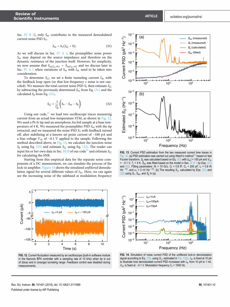
Using our code,25 we load two oscilloscope traces measuringcurrent from an actual low-temperature STM, as shown in Fig. 12.We used a Pt-Ir tip and an amorphous Au foil sample at a base tem-perature of 4 K. We measured the preamplifier PSD Saa with the tipretracted, and we measured the noise PSD Sii with feedback turnedoff, after stabilizing at a known set point current of −100 pA anda bias voltage Vdc of −0.1 V applied to the sample. Following themethod described above, in Fig. 13, we calculate the junction noiseSjj using Eq. (53) and estimate Sζζ using Eq. (32). The reader caninput his or her own data in Sec. III B of our code25 and estimate Sζζfor calculating the SNR.
Starting from this empirical data for the separate noise com-ponents of a DC measurement, we can simulate the process of thelock-in amplifier. Figure 14 shows the simulated unfiltered demodu-lation signal for several different values of Idc. Here, we can againsee the increasing noise of the sideband at modulation frequency
FIG. 12. Current fluctuation measured by an oscilloscope (built-in software modulein the Nanonis BP4 controller with a sampling rate of 10 kHz) when tip is outof (blue) and in (orange) tunneling range. Feedback control was disabled duringmeasurements.
FIG. 13. Current PSD estimation from the two measured current time traces inFig. 12. (a) PSD estimation was carried out using Welch’s method39 based on fastFourier transform. Sjj was calculated based on Eq. (53) with |Idc| = 100 pA and Vdc= −0.1 V, T j = 4 K. Saa was fitted based on the model in Sec. IV A 1 by Eqs. (51)and (52). Fitting parameters: Rf = 10 GΩ, Cf = 0.8 fF, Cs = 200 pF, in = 0.8 fAHz−1/2, and vn = 2 nV Hz−1/2. (b) The resulting Sζζ calculated by Eqs. (31) and(32) using Sii , Saa, and Sjj in (a).
FIG. 14. Simulation of noise current PSD of the unfiltered lock-in demodulationsignal according to Eq. (16), using Sζζ estimated in Fig. 13(b). Iac is fixed at 10 pAto illustrate how demodulated current PSD increases with Idc from 10 pA to 1 nA.Vdc is fixed at −0.1 V. Modulation frequency f 0 = 1000 Hz.
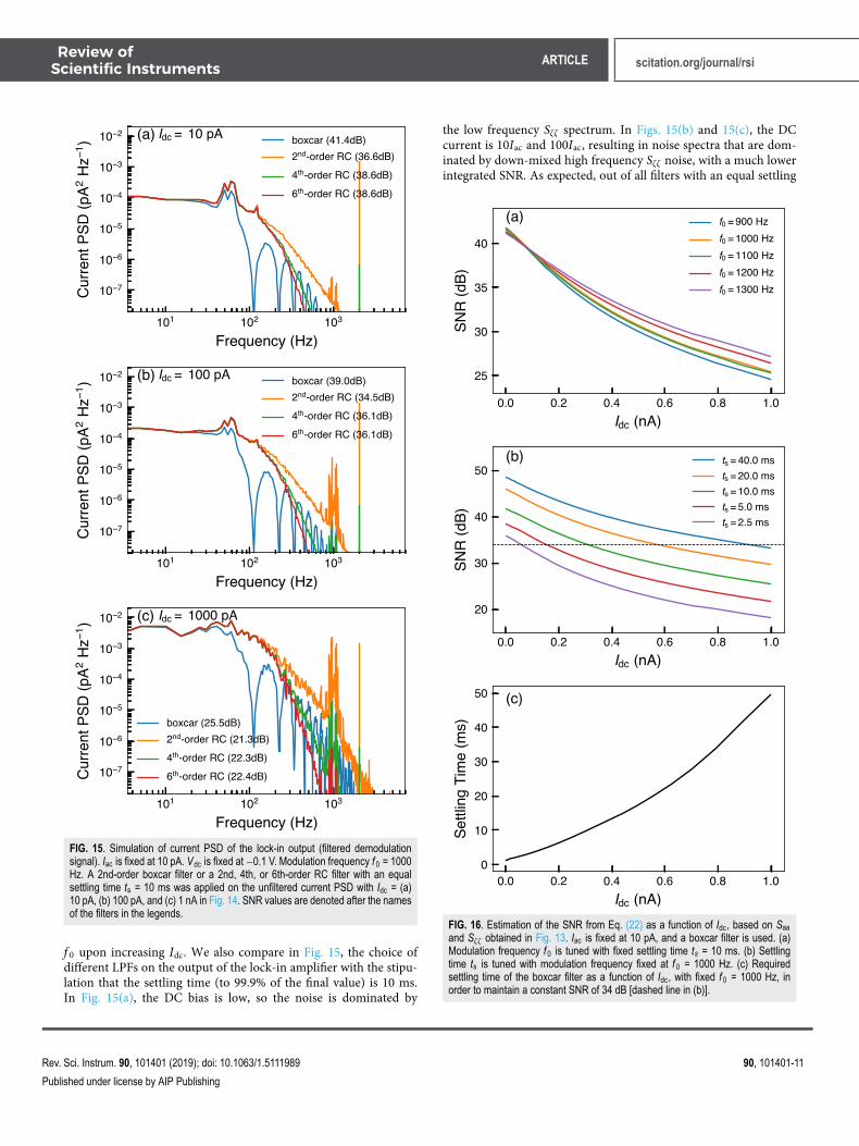
FIG. 15. Simulation of current PSD of the lock-in output (filtered demodulationsignal). Iac is fixed at 10 pA. Vdc is fixed at −0.1 V. Modulation frequency f 0 = 1000Hz. A 2nd-order boxcar filter or a 2nd, 4th, or 6th-order RC filter with an equalsettling time ts = 10 ms was applied on the unfiltered current PSD with Idc = (a)10 pA, (b) 100 pA, and (c) 1 nA in Fig. 14. SNR values are denoted after the namesof the filters in the legends.
f 0 upon increasing Idc. We also compare in Fig. 15, the choice ofdifferent LPFs on the output of the lock-in amplifier with the stipu-lation that the settling time (to 99.9% of the final value) is 10 ms.In Fig. 15(a), the DC bias is low, so the noise is dominated by
the low frequency Sζζ spectrum. In Figs. 15(b) and 15(c), the DCcurrent is 10Iac and 100Iac, resulting in noise spectra that are dom-inated by down-mixed high frequency Sζζ noise, with a much lowerintegrated SNR. As expected, out of all filters with an equal settling
FIG. 16. Estimation of the SNR from Eq. (22) as a function of Idc, based on Saa
and Sζζ obtained in Fig. 13. Iac is fixed at 10 pA, and a boxcar filter is used. (a)Modulation frequency f 0 is tuned with fixed settling time ts = 10 ms. (b) Settlingtime ts is tuned with modulation frequency fixed at f 0 = 1000 Hz. (c) Requiredsettling time of the boxcar filter as a function of Idc, with fixed f 0 = 1000 Hz, inorder to maintain a constant SNR of 34 dB [dashed line in (b)].
time of 10 ms, the boxcar filter is most effective. The reader can carryout the same analysis with various parameters such as Idc, ts, andf 0 following the same section in our Python notebook25 to predictthe current PSD of the lock-in output (see Fig. 23) and calculate thecorresponding SNR values.
Figure 16 shows for the example Saa and Sζζ how the SNRchanges when we tune modulation frequency f 0 and settling timets. A higher modulation frequency increases the SNR particularlyat a high DC current. However within a single spectroscopic mea-surement, we cannot vary the modulation frequency due to phasechange of the capacitive coupling between the tip and sample. Ingeneral, the choice of modulation frequency should be made as highas possible, without coinciding with any peak in Sii or running intothe roll-off frequency of the transimpedance preamplifier. We give ageneral step-by-step procedure for the choice of frequency in Sec. V,as there are many terms with frequency dependence in Eq. (21).On the other hand, the settling time is in principle free for theexperimenter to adjust during the measurement. In Fig. 16(b), it isstraightforward to adjust the settling time at different Idc to main-tain a constant SNR, as shown in Fig. 16(c). The reader can load hisor her own data in Sec. III B of our interactive Python notebook25
and then calculate the parameters [e.g., ts(Vdc) for the boxcar filterat some f 0] for an optimal dynamic LPF of the lock-in amplifier toapply. Most modern STM controllers have a programmable inter-face allowing users to program their own spectroscopic measure-ments and implement dynamic lock-in LPF parameters that can varywith Vdc.
IV. NOISE SOURCESSection III shows how different types of noises add to affect the
SNR of the measurement. We also showed how to measure some ofthe noise sources in a working STM, which allowed us to calculatethe expected SNR under various conditions. In this section, we willtake a more in-depth look at each noise source, in order to be able toperform noise diagnosis and design better instrumentation.
A. Transimpedance preamplifier noise S aa
The typical tunnel junction resistance Rj is usually between105Ω and 1010Ω, and the current to be measured is less than 10 nAand can be as small as 1 pA. In order to measure the small currentfrom a high-impedance source, one generally uses a transimpedanceamplifier.
1. The transimpedance amplifierWe review a complete noise model for the transimpedance
amplifier (TIA) circuit consisting of a single operational amplifier(abbreviated as opamp hereafter), as shown in Fig. 17. Most tran-simpedance amplifiers are used to read out photodiodes, whichhave fixed source impedance. The source capacitance Cs in anSTM system is usually determined by the wiring (typically a coax-ial cable of tens to hundreds of picofarad) connecting the ampli-fier to the tunnel junction. The source resistance Rs is dominatedby the tunnel junction resistance Rj, as the cable resistance istypically less than 1 kΩ, while Rj may vary between 105Ω and1010Ω.
FIG. 17. Circuit diagram for noise analysis of a TIA connected to a tunnel junction.The tunnel junction is simplified by current source I(t) and junction resistance Rs inparallel with a source capacitor Cs. The dashed triangle denotes the actual opamp,while the solid triangle denotes a “noise-free” opamp.
Below are some definitions, we will use later
Iin: input current; Zs: source impedance, connecting the signal source to the
inverting input; Zf: feedback impedance between the output and the invert-
ing input; vn: input voltage noise density of the opamp; in: input current noise density of the opamp; A: open loop gain of the opamp; β = Zs/(Zs + Zf): feedback factor (proportion of the output
voltage that appears at the inverting input); −Aβ: loop gain; V+, V−: the noninverting and inverting input voltages of the
opamp; and Vout: the output voltage of the opamp.
a. Current gain. The current gain can be found by solving thefollowing two equations:
Vout = A(V+ − V−), (33)
Iin =V− − V+
Zs+
V− − V+ − Vout
Zf. (34)
By rearranging terms, we find
Vout = (Zf
Zs+ 1)−Vout
A− IinZf = −IinZf − (Aβ)
−1Vout. (35)
Solving for Vout, we find
Vout = −IinZf(1 +1
Aβ)
−1
. (36)
In the ideal case when the loop gain Aβ≫ 1, the current gain is −Zf.
b. Noise gain. The noise gain is defined as the ratio betweenoutput voltage noise and input voltage noise. It is obtained bytreating the TIA as a noninverting voltage amplifier. As before, we
write down two equations and solve for Vout = vo as a function ofV− = vn,
vo = A(vn − V−), (37)
V− = βVout. (38)
Substituting and rearranging terms, we have
vo = vn1β(1 +
1Aβ)
−1
. (39)
In the ideal case when the loop gain Aβ ≫ 1, the noise gain is β−1.In the opposite limit when Aβ≪ 1, the noise gain is simply A (sincefeedback is ineffective with such small loop gain the amplifier acts asif it were an open loop).
The open loop gain of an opamp generally takes the form40
A( f ) =A0
1 + f /fB, (40)
where f B is the open-loop bandwidth (associated with anotherhigher-frequency roll-off which will not affect this analysis) andA0 ≫ 1 is the gain in the low frequency limit. The gain-bandwidthproduct (GBP)41 of an opamp is defined as the bandwidth at unitygain A( f ) = 1,
fGBP = A0fB. (41)
In the high frequency limit, we have A( f ) = fGBP/f . Therefore,the GBP is the one of the important metrics to compare the fre-quency performance of different opamps, and it is usually specifiedby manufacturers.
From Eq. (39), we know that after β−1( f ) curve intersects A( f ),the noise gain will follow A( f ). We now analyze the noise gain forAβ≫ 1 and sketch its behavior with frequency. We first write β−1 asa function of admittances instead of impedances,
β−1= 1 +
Zf
Zs= 1 +
Z−1s
Z−1f=
Z−1s + Z−1
f
Z−1f
. (42)
Since admittances are additive in parallel, the numerator is just theadmittance of the parallel combination of Zs and Zf, which we candefine as Zp, so
β−1=
Z−1p
Z−1f
. (43)
We now write the explicit form of the admittances in terms ofparallel resistors and capacitors,
Z−1f = R−1
f (2πjf RfCf + 1), (44a)
Z−1p = R−1
p (2πjf RpCp + 1), (44b)
where
R−1p = R−1
s + R−1f , (45a)
Cp = Cs + Cf. (45b)
So finally,
β−1=
Rf
Rp
2πjf RpCp + 12πjf RfCf + 1
. (46)
We observe the noise gain having a zero at 2πjf p, wherefp = (2πRpCp)
−1, and a pole at 2πjf C, where fC = (2πRfCf)−1 is
the bandwidth of the TIA. At low frequency, β−1→ Rf/Rp, while at
high frequency, β−1→ Cp/Cf.
In order for the TIA to be stable, the β−1 curve must inter-sect the open-loop gain curve with a relative slope of less than40 dB/decade,43 in other words, the frequency at which A( f ) = Cp/Cfmust be higher than f C, or equivalently
fGBP >Cp
CffC = (
Cs
Cf+ 1)fC ≈ 2πRfCsf 2
C , (47)
when Cf ≪ Cs. The source capacitance Cs is determined by the sumof TIA input capacitance and the capacitance of the wiring con-necting the tunnel junction to the TIA. The typical cable for a low-temperature STM has a capacitance of 50–300 pF. For example withRf = 1 GΩ, Cs = 200 pF, a stable TIA with a bandwidth of 4 kHzwould require a minimum GBP of 20 MHz, but increasing Cs to1 nF would require GBP to be above 100 MHz.
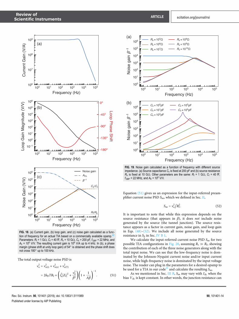
In Fig. 18, we calculate the current gain, loop gain, and noisegain for a TIA using the parameters for a commercially avail-able opamp with a GBP of 22 MHz, requiring a gain of 1 GV/Aand a bandwidth of 4 kHz, and assuming a source capacitance of200 pF. As we choose a source resistance that is much higher than thefeedback resistance, the resulting noise gain of Rf/Rp approaches 1 atlow-frequency limit. At high-frequency limit, the noise gain reachesCp/Cs, then rolls off due to finite open-loop gain. Note that the Cfrequired to obtain a bandwidth of 4 kHz is as small as 0.04 pF. Itis smaller than the typical parasitic capacitance for even the small-est surface mount resistors (usually around 0.15 pF), so it requiresthe use of multiple resistors in series with careful layout, or a morecomplex feedback network.44
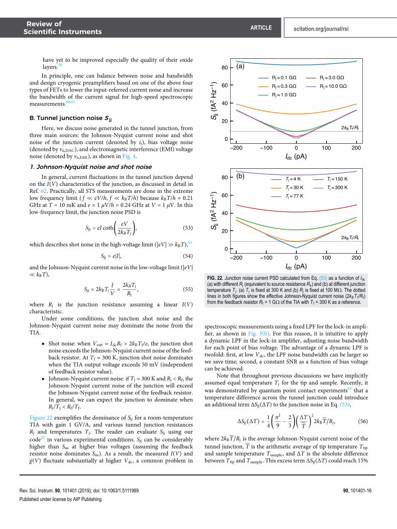
We note that the source impedance influences the noise gainin Eq. (46). In Fig. 19(a), we plot the noise gain while reducing thesource resistance from 1010 Ω to 105 Ω, which covers the rangeof most STM tunnel junction resistances. Conversely, we plot thenoise gain with a fixed source resistance Rs = 1010 Ω, but a vary-ing source capacitance from 1 pF to 10 nF in Fig. 19(b). Note thenoise gain peaks at 1nF and above, indicating an unstable TIA. Itoccurs because the GBP of 22 MHz we used is insufficient accordingto Eq. (47).
2. Input-referred noiseThe output voltage noise density is determined by three uncor-
related noise generators, which must be summed in quadrature,1. The input current noise in is amplified by the current gain,
vo(i) = −inZf(1 +1
Aβ)
−1
. (48)
2. The input voltage noise vn is amplified by the noise gain,
vo(e) =vn
β(1 +
1Aβ)
−1
. (49)
3. The Johnson-Nyquist current noise of the feedback resistor Rfappears at the output without gain,
FIG. 18. (a) Current gain, (b) loop gain, and (c) noise gain calculated as a func-tion of frequency for an actual TIA based on a commercially available opamp.42
Parameters: Rf = 1 GΩ, Cf = 40 fF, Rs = 10 GΩ, Cs = 200 pF, f GBP = 22 MHz, andA0 = 106 V/V. The resulting current gain is 109 V/A up to 4 kHz. In (b), a phasemargin (phase shift at unity loop gain) of 54 is obtained and the phase shift doesnot cross 180 up to 100 kHz.
The total output voltage noise PSD is
v2o = v2
o(i) + v2o(e) + v2
o(T)
= 2kBTRf + (i2n∣Zf∣
2 +v2
n
β2 )(1 +1
Aβ)
−1
. (51)
FIG. 19. Noise gain calculated as a function of frequency with different sourceimpedance. (a) Source capacitance Cs is fixed at 200 pF and (b) source resistanceRs is fixed at 10 GΩ. Other parameters are the same: Rf = 1 GΩ, Cf = 40 fF,f GBP = 22 MHz, and A0 = 106 V/V.
Equation (51) gives us an expression for the input-referred pream-plifier current noise PSD Saa, which we defined in Sec. II,
Saa = v2o/R
2f . (52)
It is important to note that while this expression depends on thesource resistance (that appears in β), it does not include noisegenerated by the source (the tunnel junction). The source resis-tance appears as a factor in current gain, noise gain, and loop gainin Eqs. (48)–(52). We include all noise generated by the sourceresistance in Sjj in Sec. IV B 1.
We calculate the input-referred current noise PSD Saa for twopossible TIA configurations in Fig. 20, assuming Rs ≫ Rf, showingthe contribution of each of the three noise generators along with thetotal input noise. We can see that the low-frequency noise is dom-inated by the Johnson-Nyquist current noise and/or input currentnoise, while high-frequency noise is dominated by the input voltagenoise. The reader can plug in the parameters for a desired opamp tobe used for a TIA in our code25 and calculate the resulting Saa.
As we mentioned in Sec. III B, Saa may vary with Idc when thebias Vdc is kept constant. In other words, the junction resistance can
FIG. 20. Input-referred noise current PSD of two TIA configurations based on acommercially available opamp with f GBP = 22 MHz and A0 = 106 V/V.42 (a) TheTIA with a gain of 1 GV/A and a bandwidth of 4 kHz. Parameters: Rf = 1 GΩ, Cf= 40 fF, Rs = 100 GΩ, and Cs = 200 pF. (b) The TIA with a gain of 10 GV/A anda bandwidth of 1 kHz. Parameters: Rf = 10 GΩ, Cf = 15.9 fF, Rs = 100 GΩ, andCs = 200 pF. The integrated rms current noise is (a) 2.03 pA and (b) 0.48 pA.
vary by orders of magnitude, which in turn may affect Saa at low fre-quency. We use the example of TIA shown in Fig. 20(a) and decreasethe source resistance from 100 MΩ to 0.1 MΩ. Figure 21 shows thatthe low frequency noise increased by order of magnitudes when thesource resistance is below 1 MΩ.
3. Comparison between cryogenicand room-temperature preamplifiers
From Eq. (51) and Fig. 20, we know that input voltage noisevn, amplified by noise gain β−1, dominates to Saa at high frequen-cies. The cause is the noise gain reaching a constant 1 + Cs/Cf athigh frequencies before roll-off by A( f ). In the conventional set upof an STM where the preamplifier sits outside ultrahigh vacuum(UHV) and cryogenic environment, it is difficult to reduce the noisegain because of the large wiring capacitance Cs. To minimize theinput voltage noise, one can essentially choose a low noise opamp(which may have a high input capacitance) or reduce the ratio ofCs/Cf. While increasing Cf reduces the bandwidth of the TIA, one
FIG. 21. Input-referred noise current PSD with different source resistances. TheTIA configuration is the same with Fig. 20(a), except that the input voltage noisevn is a frequency-independent constant at 4 nV Hz−1/2.
can decrease Cs by shortening the coaxial cable to a few centime-ters, which may bring the preamplifier into UHV, cryogenic envi-ronment, and physically close to the tunnel junction. It also lowersthe Johnson-Nyquist voltage noise vo(T) of the feedback resistor by afactor of 8.7 from 300 K to 4 K.
Cryogenic (first-stage) preamplifiers have been developed andimproved over decades. The central component of the opamps is thetransistor. We list four types of field effect transistors (FETs) that arecompatible with the cryogenic environment, namely, Si-based junc-tion FETs (Si-JFETs),45,46 Si-based metal-oxide-semiconductor FET(Si-MOSFETs),47–50 GaAs-based metal-semiconductor FET (GaAs-MESFETs),51–54 and GaAs-based metal-oxide-semiconductor FET(GaAs-MOSFETs).55–58 We describe the advantages and disadvan-tages of different types of FETs in the following:
1. Si-JFETs have relatively low flicker noise, but they can onlywork above 40 K due to charge freeze-out below 40 K.45,46 Inother words, JFETs have to be placed away from the 4 K bath,which contradicts our intention of reducing cable length. Inaddition, JFETs’ intrinsic input capacitance is relatively high,usually a few 10 pF.
2. Si-MOSFETs could be used below 40 K without charge freeze-out basically by transmitting more power to the conductionchannel via overrated supply voltages.47 Charge trapping ismore pronounced at low temperatures, which increases flickernoise by one order of magnitude from 300 K to 4 K.49
3. GaAs-MESFETs work based on two-dimensional electron gaswith high mobility and do not suffer from charge freeze-outat the lowest temperature. High electron mobility transistors(HEMT) are even made for preamplifiers running at megahertzfrequency with the aid of impedance matching.54,59,60 However,they require extreme care in handling and delicate matching ofunits to reduce bias shift53 and should be cooled down prop-erly to prevent telegraph noise. Intrinsic noise at 4 K measuredafter second stage voltage amplifier is not yet lower than roomtemperature preamplifiers with the same gain.53
4. GaAs-MOSFETs would be the best candidate for cryogenic sig-nal readout with their low noise and high carrier mobility but
have yet to be improved especially the quality of their oxidelayers.58
In principle, one can balance between noise and bandwidthand design cryogenic preamplifiers based on one of the above fourtypes of FETs to lower the input-referred current noise and increasethe bandwidth of the current signal for high-speed spectroscopicmeasurements.60,61
B. Tunnel junction noise S jj
Here, we discuss noise generated in the tunnel junction, fromthree main sources: the Johnson-Nyquist current noise and shotnoise of the junction current (denoted by ij), bias voltage noise(denoted by vn,DAC), and electromagnetic interference (EMI) voltagenoise (denoted by vn,EMI), as shown in Fig. 4.
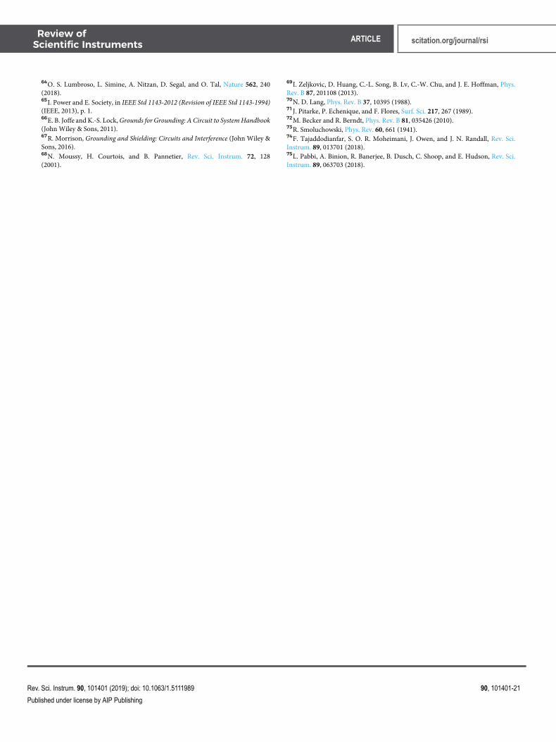
1. Johnson-Nyquist noise and shot noiseIn general, current fluctuations in the tunnel junction depend
on the I(V) characteristics of the junction, as discussed in detail inRef. 62. Practically, all STS measurements are done in the extremelow frequency limit ( f ≪ eV/h, f ≪ kBT/h) because kBT/h = 0.21GHz at T = 10 mK and e × 1 μV/h = 0.24 GHz at V = 1 μV. In thislow-frequency limit, the junction noise PSD is
Sjj = eI coth(eV
2kBTj), (53)
which describes shot noise in the high-voltage limit (|eV|≫ kBT),63
Sjj = e∣I∣, (54)
and the Johnson-Nyquist current noise in the low-voltage limit (|eV|≪ kBT),
Sjj = 2kBTjIV=
2kBTj
Rj, (55)
where Rj is the junction resistance assuming a linear I(V)characteristic.
Under some conditions, the junction shot noise and theJohnson-Nyquist current noise may dominate the noise from theTIA.
Shot noise: when Vout = IdcRf > 2kBTf/e, the junction shotnoise exceeds the Johnson-Nyquist current noise of the feed-back resistor. At Tf = 300 K, junction shot noise dominateswhen the TIA output voltage exceeds 50 mV (independentof feedback resistor value).
Johnson-Nyquist current noise: if T j = 300 K and Rj < Rf, theJohnson-Nyquist current noise of the junction will exceedthe Johnson-Nyquist current noise of the feedback resistor.In general, we can expect the junction to dominate whenRj/T j < Rf/Tf.
Figure 22 exemplifies the dominance of Sjj for a room-temperatureTIA with gain 1 GV/A, and various tunnel junction resistancesRj and temperatures T j. The reader can evaluate Sjj using ourcode25 in various experimental conditions. Sjj can be considerablyhigher than Saa at higher bias voltages (assuming the feedbackresistor noise dominates Saa). As a result, the measured I(V) andg(V) fluctuate substantially at higher Vdc, a common problem in
FIG. 22. Junction noise current PSD calculated from Eq. (53) as a function of Idc(a) with different Rj (equivalent to source resistance Rs) and (b) at different junctiontemperature T j. (a) T j is fixed at 300 K and (b) Rj is fixed at 100 MΩ. The dottedlines in both figures show the effective Johnson-Nyquist current noise (2kBT f/Rf)from the feedback resistor Rf = 1 GΩ of the TIA with T f = 300 K as a reference.
spectroscopic measurements using a fixed LPF for the lock-in ampli-fier, as shown in Fig. 3(b). For this reason, it is intuitive to applya dynamic LPF in the lock-in amplifier, adjusting noise bandwidthfor each point of bias voltage. The advantage of a dynamic LPF istwofold: first, at low Vdc, the LPF noise bandwidth can be larger sowe save time; second, a constant SNR as a function of bias voltagecan be achieved.
Note that throughout previous discussions we have implicitlyassumed equal temperature T j for the tip and sample. Recently, itwas demonstrated by quantum point contact experiments64 that atemperature difference across the tunnel junction could introducean additional term ΔSjj(ΔT) to the junction noise in Eq. (53),
ΔSjj(ΔT) =14(π2
9−
23)(
ΔTT)
22kBT/Rj, (56)
where 2kBT/Rj is the average Johnson-Nyquist current noise of thetunnel junction, T is the arithmetic average of tip temperature Ttipand sample temperature Tsample, and ΔT is the absolute differencebetween Ttip and Tsample. This excess term ΔSjj(ΔT) could reach 15%
of the average junction Johnson-Nyquist current noise if the tem-perature of one side of the junction is 4 times the temperature of theother side (e.g., Tsample = 1 K but Ttip = 4 K). Therefore, in STMdesign, one should consider thermal anchoring, not only for thesample but also for the tip, to minimize the temperature differencebetween them.
2. Bias voltageBias voltage noise contributes to junction noise as well, in the
form of vn,DAC/Rj, as shown in Fig. 4. For a typical 20-bit digital-to-analog converter (DAC) with a range of ±10 V and speed up to106 samples/s, the output voltage has a noise floor of around 20 nVHz−1/2. It is comparable to the Johnson-Nyquist voltage noise of atunnel junction of 2 MΩ at 4 K. For the typical working range ofSTM, the voltage noise of DACs for the bias voltage is thus neg-ligible, but we will see in Sec. IV C 1 that vn,DAC enters Sζζ afteramplification.
3. Electromagnetic interferenceWe include electromagnetic interference (EMI) in the junction
current noise, though technically the electromagnetic noise pick-upcould occur not only at the tunnel junction but also in the wiring.At high frequency, EMI is known as radio-frequency noise, coupledvia radiation to the whole STM circuitry. If the STM unit is wellshielded, then the interference mostly occurs in the wires and cablesrunning from the controllers to the STM. At low frequency, EMIexhibits as ground-loop induction, usually at the line frequency andits harmonics. The noise sources, however, are not intrinsic. Elimi-nating EMI is a topic extensively discussed in the literature,65–67 andit should be carried out prior to STM noise characterization.
C. Tip-sample distance modulation noise S ζζ
Tip-sample distance fluctuation introduces noise that scaleswith the signal (both AC and DC); therefore, the power of dimen-sionless quantity ζ appears in the SNR of Eq. (21). In this section, wediscuss three factors that influence Sζζ : piezo control voltage noise,fluctuation of apparent barrier height, and mechanical vibration.
1. Piezo control voltage noiseIn STM, we actuate the tip by applying a high voltage across
the scanner piezos. A standard sample with a known lattice (e.g., Sior Au crystal) is used to calibrate the piezo motion with respect toapplied voltage. The calibration factor is usually on the order of afew nanometers per volt. On the other hand, in the feedback loop,an error signal between instantaneous value and set point of the cur-rent is generated, and it adds to the z piezo voltage to move the tipaccordingly to maintain a constant current. The error signal is lowvoltage (an output of a DAC) and amplified by a high voltage ampli-fier (HVA). Additionally, the DAC output noise, which accompaniesthe error signal, is amplified with the same gain. The total controlvoltage noise is the sum of the amplified noise and the output volt-age noise of the HVA itself (even when the feedback loop is open),as shown in Fig. 4. As a consequence, one can estimate tip-sampledistance modulation due to noise from piezo control voltage. Forinstance, frequency-independent noise with an amplitude spectraldensity of 1 μV Hz−1/2 multiplied by a 1 nm/V calibration factor
results in 1 fm Hz−1/2 in the z direction. After the conversion, onecan compare the piezo control voltage noise with the mechanicalvibration.
When spectroscopic measurements are being performed, thefeedback loop is open in order to have a constant tip-sample dis-tance. In this case, any fluctuation in HVA outputs (not only z butalso x and y) would cause fluctuation in the tip-sample distance. Onecan add switchable low pass filters (with a cutoff frequency on theorder of ∼0.5 Hz) after the HVA outputs68 and activate the LPFsfor the HVA outputs to attenuate AC noise from the DACs andthe HVA (only during spectroscopy, as the feedback control signalwould also be attenuated in the closed feedback loop). Furthermore,as DC drift cannot be filtered out by the LPFs of the HVA outputs,care must be taken to avoid substantial temperature changes in theHVAs, since input offset voltage could drift ∼0.05 mV/C, whichyields ∼1 pm/C at a gain of 20. This temperature change is concern-ing because the HVAs draw considerable power (∼5 W per opamp),so sufficient air cooling must be implemented for the HVAs.
2. Apparent barrier heightIn Eq. (6), we treat κ as a constant, or at least insensitive to
change in bias voltage or tip-sample distance, which is generallythe case. Here, we need to emphasize that in some situations κ mayvary spatially69 or as a function of applied bias voltage,8 which effec-tively introduces fluctuation in current. For a rectangular tunnelbarrier,70,71
κ =2h√
2mϕa, (57)
where ϕa is the apparent barrier height, usually considered as a con-stant yielding to the average work function of the tip and sample.However, experiments72 show that close to crystal step edges, dueto dipole moment build-up (Smoluchowski effect73), ϕa varies withapplied voltage up to ∼15%/V in the intermediate bias range. Fur-thermore, local chemical potential on the sample surface may fluctu-ate spatially and result in variation of κ by as much as 60%.69 Com-pensations methods based on local barrier height measurements74
are needed for such samples before performing spectroscopic mea-surements.
3. Mechanical vibrationThe other part in the dimensionless quantity ζ is the fluctuation
in tip-sample distance zn(t). Since κ is typically 2 Å−1, zn exceeding1 pm results in 2% variation in the current signal. The environmentalnoise, mainly mechanical vibration and acoustic noise, could easilyexcite zn over 1 pm if the tip-sample junction is lightly coupled to thelaboratory environment. To minimize the acoustic noise, one canmove all the sound sources out and apply sound absorbing materialson the walls of the lab room. On the other hand, mechanical vibra-tion is always a major concern in system design of all STMs. Vibra-tion transfer is quantified by the overall structure transfer functionK in Fig. 4, which is approximately35
K( f ) ≈ (fI
fS)
2
, (58)
where f I and f S are natural frequencies of the isolators and STM,respectively. It is immediately clear that one should increase f S anddecrease f I to minimize vibration noise. First, multistage isolators
including suspension springs, pneumatic systems, and eddy-currentdampers are commonly used to decrease f I but limited down to∼1 Hz; second, it is important to improve the stiffness-to-weightratio of the STM unit in order to increase f S; and third, an alter-nate approach is feasible to measure the transfer function and applyreal-time (synchronized) vibration cancellation to the current sig-nal. Since it is beyond the scope of this article, here, we direct thereaders to one good example of each method, in Refs. 53, 59, and 75,respectively.
V. CONCLUSIONIn this article, we give an explicit expression for the SNR in
scanning tunneling spectroscopy, a flowchart to decompose the var-ious noise sources and their relations, and a computer code25 toestimate each noise source and to predict the SNR with differentexperimental parameters. We provide an example of noise in anactual STM, give suggestions for low-pass filters of the lock-in ampli-fier to enhance the SNR, and offer methods to keep the SNR constantduring a spectroscopic measurement. We discuss in detail the noisesources from the transimpedance preamplifier, the tunnel junc-tion, and the tip-sample distance fluctuation. Through iterationsof eliminating or suppressing the noisiest source, one can achievea stable low noise condition in scanning tunneling spectroscopicmeasurements.
As pointed out in Sec. I, time is the major limiting factor inQPI imaging with atomic resolution. We suggest an algorithm tooptimize the SNR in single-point spectroscopy before launching alengthy QPI measurement that lasts a few days.
1. Measure Saa by withdrawing the tip by a few nanometers[Figs. 12 and 13(a)] and compare it with the model Saa inSec. IV A 1 or noise specification curves if a commercialpreamplifier is used. Suppress all extra noise peaks (normallyat the line frequency and its harmonics) by inspecting EMIintroduced to the system.
2. Measure Sii in a DC measurement [Figs. 12 and 13(a)] at thedesired setup bias voltage and current set point with feed-back control disabled, and extract Sζζ according to Eq. (32)[Fig. 13(b)].
3. Find corner frequency f F of flicker noise (Fig. 1) and com-pare flicker noise power PF with preamplifier noise Pamp usingEq. (4). If PF > Pamp, the lock-in method should be appliedfor STS measurements; otherwise, the DC method should beused.
4. Inspect noise peaks in Sζζ and suppress the correspondingenvironment vibration noise sources if possible.
5. Pick an initial modulation frequency f 0 that has a low noisespectral density in Sii. Note that f 0 cannot be larger than f amp.
6. Perform a single STS measurement for converting Vdc to Idc[Fig. 3(a)] and obtaining the ratio of Idc/Iac as a function ofVdc.
7. Calculate the SNR as a function of Vdc with Eq. (22), usingthe relation between Idc/Iac and Vdc obtained in the previousstep.
8. Calculate the SNR as a function of modulation frequencyf 0 [Fig. 16(a)] and change f 0 to a frequency that has anoverall higher SNR in the measured range of Idc. Note thatboth f 0 and 2f 0 should be away from frequencies of existing
noise peaks to avoid considerable cross-correlation terms inEq. (12).
9. Calculate the filter parameters for the lock-in amplifier, suchas settling time of boxcar or RC filter as a function of Vdc tokeep the SNR constant (Fig. 11).
10. Apply the dynamic low-pass filter from the previous step tothe lock-in amplifier and perform another STS measurementto check the SNR [Fig. 3(a)]. Iterate steps 5–9 until a constantSNR is achieved.
Once the SNR is optimized in single-point spectroscopic mea-surements, one typically saves time at low bias voltages, where theSNR is generally higher than the SNR at higher bias voltages for astatic LPF of the lock-in amplifier (Fig. 16). We also recommend test-ing the dynamic LPF setting for the lock-in amplifier on a few spatiallocations. By improving noise conditions and dynamically optimiz-ing the LPF parameters of the lock-in amplifier, efficiency can besubstantially increased in STS measurements and QPI imaging.
ACKNOWLEDGMENTSThis work was supported by the National Science Founda-
tion under Grant No. DMR-1231319 (STC Center for IntegratedQuantum Materials).
Symbolsg differential conductance (A V−1)I current (A)i current noise (A)r spatial location (m, Å)V voltage (V)v voltage noise (V)q momentum transfer (m−1, Å−1)k momentum (m−1, Å−1)P power of the current (A2)t time (s)
T temperature (K)f frequency (Hz)κ current decay constant (m−1, Å−1)z tip-sample distance (m, Å−1)ζ dimensionless fluctuation factor [Eq. (8c)] (1)δ dirac delta functionS power spectral densityj unit imaginary numbere elementary charge (C)R resistance (Ω)H frequency response functionp specific current power (1)BN equivalent noise bandwidth (Hz)h impulse response function in the time domainy step response function in the time domainC capacitance (F)Z impedance (V A−1)A open loop gain (1)β feedback factorkB Boltzmann constant (J K−1, eV K−1)
FIG. 23. (a) Estimated PSDs of the tip out of (blue) and in (orange) tunneling range.The measurements (current traces not shown) were carried out with a PtIr tip andCeBi sample at 4 K with feedback control disabled. Setup conditions: Vdc = 0.4 Vand Idc = 1 nA. The corresponding Sjj was calculated based on Eq. (53). (b) Sζζcalculated by Eqs. (31) and (32) using Sii , Saa, and Sjj in (a).
ϕa apparent barrier height (J, eV)K mechanical transfer function
APPENDIX: OMISSION OF THE CROSS-CORRELATIONTERMS IN THE NOISE POWER SPECTRUM DENSITY
We derive Eq. (14) in Sec. II A from Eq. (12) with the approxi-mation that cross-correlation terms between the same function withdifferent frequency shifts, such as ζ( f − f 0)ζ∗( f − 2f 0), vanish. Asζ( f ) is unknown [we can only estimate its PSD by Eq. (32)], herewe show an example comparison between the simulated and exper-imentally measured Sii|H( f )|2 to empirically demonstrate it to be agood approximation.
We estimate Sζζ by the method described in Sec. III B withEqs. (30)–(32) in a different STM setup, and the resulting PSDs areshown in Fig. 23.
Following Eq. (16), we can simulate Sii of unfiltered lock-indemodulation signal with parameters Iac = 10 pA, Idc = 1 nA,
FIG. 24. Comparison between simulated and experimental noise current of thelock-in output. (a) Lock-in output measured by an oscilloscope (sampling rate10 kHz) when the tip is in the tunneling range with feedback disabled and biasmodulation activated. Setup conditions: Vdc = 0.4 V, Idc = 1.0 nA, Vac = 3.5 mV,and f 0 = 1170 Hz. (b) Simulated (orange) and experimental (blue) current PSDSii |H(f )|2 of the lock-in output. A simple boxcar filter with ts = (2πf0)
−1 is appliedafter the lock-in demodulation. The experimental PSD is evaluated by Welch’smethod from (a), while the simulated PSD is calculated by applying the boxcarfilter to Sii estimated from Eq. (16).
Vdc = 0.4 V, and f 0 = 1170 Hz. While the measurable PSD is thefiltered lock-in demodulation signal, we apply a simple boxcar filterto Sii as shown by the orange spectrum in Fig. 24(b). We measurethe actual lock-in output with exactly the same parameters in thesimulation in Fig. 24(a). The estimated PSD is shown by the bluespectrum in Fig. 24(b). The simulation agrees well with the exper-imental result, with an average underestimation of Sii of 5%. Thisexample indicates that Eq. (16) provides an excellent estimation ofthe noise PSD of the lock-in demodulation signal.
REFERENCES1A. Selloni, P. Carnevali, E. Tosatti, and C. D. Chen, Phys. Rev. B 31, 2602(1985).2J. A. Stroscio, R. Feenstra, and A. Fein, Phys. Rev. Lett. 57, 2579 (1986).3M. F. Crommie, C. P. Lutz, and D. M. Eigler, Nature 363, 524 (1993).4Y. Hasegawa and P. Avouris, Phys. Rev. Lett. 71, 1071 (1993).5J. Hoffman, K. McElroy, D.-H. Lee, K. Lang, H. Eisaki, S. Uchida, and J. Davis,Science 297, 1148 (2002).6T. Hanaguri, C. Lupien, Y. Kohsaka, D.-H. Lee, M. Azuma, M. Takano, H.Takagi, and J. Davis, Nature 430, 1001 (2004).7M. Allan, A. Rost, A. Mackenzie, Y. Xie, J. Davis, K. Kihou, C. Lee, A. Iyo,H. Eisaki, and T.-M. Chuang, Science 336, 563 (2012).8D. Huang, C.-L. Song, T. A. Webb, S. Fang, C.-Z. Chang, J. S. Moodera,E. Kaxiras, and J. E. Hoffman, Phys. Rev. Lett. 115, 017002 (2015).9J. Lee, M. Allan, M. Wang, J. Farrell, S. Grigera, F. Baumberger, J. Davis, andA. Mackenzie, Nat. Phys. 5, 800 (2009).10A. R. Schmidt, M. H. Hamidian, P. Wahl, F. Meier, A. V. Balatsky, J. Garrett,T. J. Williams, G. M. Luke, and J. Davis, Nature 465, 570 (2010).11B. B. Zhou, S. Misra, E. H. da Silva Neto, P. Aynajian, R. E. Baumbach,J. Thompson, E. D. Bauer, and A. Yazdani, Nat. Phys. 9, 474 (2013).12G. M. Rutter, J. N. Crain, N. P. Guisinger, T. Li, P. N. First, and J. A. Stroscio,Science 317, 219 (2007).13T. Zhang, P. Cheng, X. Chen, J.-F. Jia, X. Ma, K. He, L. Wang, H. Zhang, X. Dai,Z. Fang, X. Xie, and Q.-K. Xue, Phys. Rev. Lett. 103, 266803 (2009).14H. Beidenkopf, P. Roushan, J. Seo, L. Gorman, I. Drozdov, Y. San Hor,R. J. Cava, and A. Yazdani, Nat. Phys. 7, 939 (2011).15I. Zeljkovic, Y. Okada, C.-Y. Huang, R. Sankar, D. Walkup, W. Zhou, M. Serbyn,F. Chou, W.-F. Tsai, H. Lin, A. Bansil, L. Fu, M. Z. Hasan, and V. Madhavan, Nat.Phys. 10, 572 (2014).16H. Zheng, G. Bian, G. Chang, H. Lu, S.-Y. Xu, G. Wang, T.-R. Chang, S. Zhang,I. Belopolski, N. Alidoust, D. S. Sanchez, F. Song, H.-T. Jeng, N. Yao, A. Bansil,S. Jia, H. Lin, and M. Z. Hasan, Phys. Rev. Lett. 117, 266804 (2016).17L. Perfetti, P. Loukakos, M. Lisowski, U. Bovensiepen, H. Berger, S. Biermann,P. Cornaglia, A. Georges, and M. Wolf, Phys. Rev. Lett. 97, 067402 (2006).18F. Schmitt, P. S. Kirchmann, U. Bovensiepen, R. G. Moore, L. Rettig, M. Krenz,J.-H. Chu, N. Ru, L. Perfetti, D. Lu, M. Wolf, I. Fisher, and Z. X. Shen, Science 321,1649 (2008).19Y. Wang, D. Hsieh, E. Sie, H. Steinberg, D. Gardner, Y. Lee, P. Jarillo-Herrero,and N. Gedik, Phys. Rev. Lett. 109, 127401 (2012).20A. Damascelli, Z. Hussain, and Z.-X. Shen, Rev. Mod. Phys. 75, 473 (2003).21C. Tusche, A. Krasyuk, and J. Kirschner, Ultramicroscopy 159, 520 (2015).22M. Lawler, K. Fujita, J. Lee, A. Schmidt, Y. Kohsaka, C. K. Kim, H. Eisaki,S. Uchida, J. Davis, J. Sethna et al., Nature 466, 347 (2010).23M. Hamidian, I. Firmo, K. Fujita, S. Mukhopadhyay, J. Orenstein, H. Eisaki,S. Uchida, M. Lawler, E. Kim, and J. Davis, New J. Phys. 14, 053017 (2012).24The definitions in Eqs. (1) and (2) can be used for any signal of interest X(t),with x(t) being its accompanying noise. In Sec. II, the signal of interst is thedemodulated current measured at the output of the lock-in amplifier.25See https://github.com/Let0n/achievinglownoiseinsts for our interactive Pythoncode.26x( f ) is commonly known as amplitude spectral density, and its unit is the unitof x(t) times Hz−1/2.
27A. Van der Ziel, Proc. IEEE 76, 233 (1988).28P. H. Handel, Phys. Rev. Lett. 34, 1492 (1975).29C. T. J. Alkemade, W. Snelleman, G. Boutilier, B. Pollard, J. Winefordner,T. Chester, and N. Omenetto, Spectrochim. Acta, Part B 33, 383 (1978).30G. Boutilier, B. Pollard, J. Winefordner, T. Chester, and N. Omenetto,Spectrochim. Acta, Part B 33, 401 (1978).31C. T. J. Alkemade, W. Snelleman, G. Boutilier, and J. Winefordner, Spectrochim.Acta, Part B 35, 261 (1980).32The amplitude of the demodulating multiplier is set to unity here. If this ampli-tude is unknown in practice, the differential conductance g(V) can be normalizedmanually by the numerically differentiated I(V).33This demodulation signal is normally inaccessible and not an actual output ofthe lock-in amplifier, but a mathematical result from the lock-in demodulationprocess. The actual accessible output of the lock-in amplifier is located after itsLPF, as shown by Iac,x and Iac,y in Fig. 2(a).34The last term is calculated by Fourier transform of the square of Iac cos(4πf 0t)in Eq. (10) to avoid ill-defined δ2( f ± 2f 0).35C. J. Chen, Introduction to Scanning Tunneling Microscopy, 2nd ed. (OxfordUniversity Press, Oxford, 1993), Chap. 14.36D. White and J. Clare, Meas. Sci. Technol. 3, 1 (1992).37E. Voigtman and J. D. Winefordner, Rev. Sci. Instrum. 57, 957 (1986).38See https://www.thinksrs.com/downloads/pdfs/catalog/SR556c.pdf for specifi-cations of the preamplifier.39P. Welch, IEEE Trans. Audio Electroacoust. 15, 70 (1967).40S. Srinivasan, Int. J. Electron. 42, 141 (1977).41G. De Geronimo, G. Bertuccio, and A. Longoni, Rev. Sci. Instrum. 67, 2643(1996).42See http://www.ti.com/product/OPA827 for specifications of the opamp.43R. Mancini, Op Amps for Everyone: Design Reference, 2nd ed. (Newnes, Amster-dam, London, 2003), Chap. 8.44G. Giusi, G. Cannatà, G. Scandurra, and C. Ciofi, Int. J. Circuit Theory Appl. 43,1455 (2015).45F. M. Klaassen and J. R. Robinson, IEEE Trans. Electron Devices 17, 852 (1970).46S. S. Sesnic and G. R. Craig, IEEE Trans. Electron Devices 19, 933 (1972).47J. T. Hastings and K. Ng, Rev. Sci. Instrum. 66, 3691 (1995).48H. Birk, K. Oostveen, and C. Schönenberger, Rev. Sci. Instrum. 67, 2977(1996).49Z. Švindrych, Z. Janu, F. Soukup, and R. Tichý, Cryogenics 48, 160 (2008).50C. Zhang, H. Jeon, M. Oh, M. Lee, S. Kim, S. Yi, H. Lee, I. Zoh, Y. Yoo, andY. Kuk, Rev. Sci. Instrum. 88, 066109 (2017).51A. T.-J. Lee, Rev. Sci. Instrum. 64, 2373 (1993).52S. Urazhdin, S. Tessmer, and R. Ashoori, Rev. Sci. Instrum. 73, 310 (2002).53Y. J. Song, A. F. Otte, V. Shvarts, Z. Zhao, Y. Kuk, S. R. Blankenship, A. Band,F. M. Hess, and J. A. Stroscio, Rev. Sci. Instrum. 81, 121101 (2010).54Q. Dong, Y. Liang, D. Ferry, A. Cavanna, U. Gennser, L. Couraud, and Y. Jin,Appl. Phys. Lett. 105, 013504 (2014).55K. Rajagopalan, J. Abrokwah, R. Droopad, and M. Passlack, IEEE ElectronDevice Lett. 27, 959 (2006).56S. Oktyabrsky and D. Y. Peide, Fundamentals of III-V Semiconductor MOSFETs(Springer, 2010).57R. Terao, T. Kanazawa, S. Ikeda, Y. Yonai, A. Kato, and Y. Miyamoto, Appl.Phys. Express 4, 054201 (2011).58Y. Xuan, Y. Q. Wu, H. C. Lin, T. Shen, and P. D. Ye, IEEE Electron Device Lett.28, 935 (2007).59I. Battisti, G. Verdoes, K. van Oosten, K. M. Bastiaans, and M. P. Allan, Rev. Sci.Instrum. 89, 123705 (2018).60F. Massee, Q. Dong, A. Cavanna, Y. Jin, and M. Aprili, Rev. Sci. Instrum. 89,093708 (2018).61K. Bastiaans, T. Benschop, D. Chatzopoulos, D. Cho, Q. Dong, Y. Jin, andM. Allan, Rev. Sci. Instrum. 89, 093709 (2018).62D. Rogovin and D. Scalapino, Ann. Phys. 86, 1 (1974).63Here, we use the fact that I and V share the same sign, and coth ( eV
64O. S. Lumbroso, L. Simine, A. Nitzan, D. Segal, and O. Tal, Nature 562, 240(2018).65I. Power and E. Society, in IEEE Std 1143-2012 (Revision of IEEE Std 1143-1994)(IEEE, 2013), p. 1.66E. B. Joffe and K.-S. Lock, Grounds for Grounding: A Circuit to System Handbook(John Wiley & Sons, 2011).67R. Morrison, Grounding and Shielding: Circuits and Interference (John Wiley &Sons, 2016).68N. Moussy, H. Courtois, and B. Pannetier, Rev. Sci. Instrum. 72, 128(2001).
69I. Zeljkovic, D. Huang, C.-L. Song, B. Lv, C.-W. Chu, and J. E. Hoffman, Phys.Rev. B 87, 201108 (2013).70N. D. Lang, Phys. Rev. B 37, 10395 (1988).71J. Pitarke, P. Echenique, and F. Flores, Surf. Sci. 217, 267 (1989).72M. Becker and R. Berndt, Phys. Rev. B 81, 035426 (2010).73R. Smoluchowski, Phys. Rev. 60, 661 (1941).74F. Tajaddodianfar, S. O. R. Moheimani, J. Owen, and J. N. Randall, Rev. Sci.Instrum. 89, 013701 (2018).75L. Pabbi, A. Binion, R. Banerjee, B. Dusch, C. Shoop, and E. Hudson, Rev. Sci.Instrum. 89, 063703 (2018).