E. Pavarini, E. Koch, J. van den Brink, and G. Sawatzky (eds.)Quantum Materials: Experiments and TheoryModeling and Simulation Vol. 6Forschungszentrum Julich, 2016, ISBN 978-3-95806-159-0http://www.cond-mat.de/events/correl16
During the last 15–20 years, scanning tunneling microscopy and spectroscopy (STM/STS) has
developed into an indispensable experimental tool of modern condensed matter physics. This
method provides real-space dependent spectroscopic information of a solid’s surface at the
atomic scale. It is thus capable to directly observe quantum mechanical effects, which in turn
provide new insight into the properties of a solid, which includes, remarkably, even momentum-
resolved information on electronic states.
The purpose of this lecture is to convey the main experimental concepts of STM/STS for the
research on correlated materials. Thereby, it cannot and does not aim at comprehensively cov-
ering STM/STS work on all kinds of different material classes of correlated systems. The focus
will be specifically on unconventional superconductors, which are, among the electronically
correlated materials, the most prominent ones where STM/STS has been successfully used,
providing new ground-breaking insights. After a more general introduction to the experiment
itself, the lecture will first specifically address the unconventional superconductor LiFeAs, for
which comprehensive STM/STS data of high quality exist and which is still a matter of ongo-
ing research. This will be complemented by briefly summarizing fundamental work on cuprate
superconductors. It can be expected readers who digest the thereby introduced techniques and
concepts will be able to easily access other existing and future work on correlated materials
with STM/STS.
2 Basics
2.1 Methods
We consider an atomically sharp metallic tip that is brought into close distance (a few Angstroms)
to the surface of a solid, i.e. the sample which we would like to investigate. In this situation,
electrons tunnel from the tip to the sample and vice versa. If both are at the same electrochem-
ical potential the net current will be zero. A finite net tunneling current will, however, arise
when we apply an electrical bias voltage Ubias between the tip and the sample [1–3]
I = A|M |2N0
∫
∞
−∞
ρs(E)[f(E)− f(E − eUbias)] dE , (1)
with A a constant of proportionality, M the tunneling matrix element, and f the Fermi distribu-
tion function. N0 and ρs are the density of states (DOS) of the tip and the local density of states
(LDOS) of the sample at the position of the tip, respectively. Note that already in Eq. (1) signif-
icant approximations have been made which we will assume to be valid throughout this chapter
unless stated otherwise: Both N0 and |M |2 are assumed to be energy independent, and thus can
be written in front of the integral. Approximate energy independence can be achieved for the
former by using an appropriate tip material. For the latter it is reasonably valid at small Ubias
and for sufficiently simple electronic structure (see e.g. [4] for a more elaborate discussion).
Scanning Tunneling Spectroscopy 14.3
It has been shown further – and this is crucial for the exploitation of the tunneling current for
microscopy – that the tunneling matrix element decays exponentially with increasing distance
d between the tip and the sample [2, 3], viz. I ∝ e−2κd, where κ depends on the work functions
of the sample and the tip. This means the well known exponentially decaying tunneling prob-
ability for one-dimensional electron tunneling depending on the width of the vacuum barrier is
recovered. The other crucial finding from Eq. (1) is that, at temperature T = 0, the tunneling
current I is proportional to the LDOS of the sample integrated between the Fermi level ǫF and
ǫF + eUbias. At finite temperature, this energy interval is, of course, broadened through the
Fermi functions.
2.1.1 Scanning tunneling microscopy (STM)
In a scanning tunneling microscope, the relative position of the tunneling tip to the sample can
be controlled in the three spatial dimensions x, y parallel and z perpendicular to the sample’s
surface, where nowadays a precision in the picometer range can be achieved (see e.g. [4, 5] for
details on the technical realization). This opens up a plethora of possibilities for probing the
surface of a sample. A fundamentally important measurement mode is scanning tunneling
microscopy (STM), i.e., a high-resolution measurement of the surface topography. A very
important way to do this (among others) is the so-called constant-current topography mode:
The actuator for tip motion along the z-direction is connected to a feed-back loop that measures
the tunneling current I and maintains it constant during scanning the tip in the (x, y)-plane
by appropriately adjusting the z-position of the tip which regulates the distance d between tip
and sample. Inspection of Eq. (1) tells us that the resulting data set z(x, y) describes a plane of
constant integrated LDOS of the sample (within ǫF and ǫF +eUbias). Due to the very high lateral
and vertical resolution in STM, it is possible to resolve even the atomic corrugation of a surface.
Fig. 1 depicts representative data taken from 2H-NbSe2. This compound exhibits a charge
density wave (CDW) at low temperature, yielding a 3 × 3 superlattice [6]. The topographic
STM data in Fig. 1 very clearly reveal this superstructure [8], which highlights that the STM is
susceptible to the spatial modulations of the electronic LDOS (which in the present example is
generated by the CDW). Further below, we shall see more examples of spatial modulations in
the LDOS which can be detected in STM.
2.1.2 Scanning tunneling spectroscopy (STS)
Eq. (1) implies that through measuring the tunneling current as a function of Ubias, the LDOS
of the sample at a fixed position of the tip, i.e. ρs(E) with E = eUbias, can be accessed. In the
experiments, the differential conductance
dI
dU
∣
∣
∣
∣
U=Ubias
∝
∫
∞
−∞
ρs(E)∂f(E − eU)
∂(eU)
∣
∣
∣
∣
U=Ubias
dE, (2)
is evaluated, either by numerical derivation or by directly measuring it using a lock-in amplifier
(see [4, 5] for details). Eq. (2) describes the convolution of ρs with the voltage derivative of the
14.4 Christian Hess
high low
2.0 nm
a
Hei
ght
Å[]
0 1 2 3 4 5 60.00.20.40.60.81.01.21.4
Distance [nm]
b
Fig. 1: (a) Constant current topographic image of 2H-NbSe2 in a field of view of 10 nm×10 nm,
Ubias = −200 mV, I = 0.7 nA, T = 10 K. The topography shows the atomic corrugation of the
topmost layer of Se atoms, and reveals the CDW with a periodicity of 3a × 3a with the lattice
constant a = 0.0345 nm [7]. (b) Line section taken along the arrow. Image and graph taken
from [8].
Fermi distribution function which is a bell-shaped curve centered around Ubias with a FWHM of
about 3.5 kBT . Thus, the spectroscopic resolution in energy ∆E is inevitably thermally broad-
ened. Scanning tunneling spectroscopy (STS) with high energy resolution therefore requires
measurements at very low temperatures. Typical values for ∆E at the cryogenically relevant
temperatures 300 mK and 4.2 K are 90 µeV and 1.3 meV, respectively.
In a scanning tunneling microscope, spectroscopic measurements of the differential conduc-
tance dI/dU can be performed as a function of the spatial tip position, which provides the
unique possibility to map out the energy dependent LDOS as a function of the (x, y) position.
The resulting data for ρs(E, x, y) are often false-color plotted in a two-dimensional fashion as
a function of (x, y) at a fixed E = eUbias, a technique often called Spectroscopic Imaging (SI-
STM). The resulting images provide valuable information about the energy dependence of the
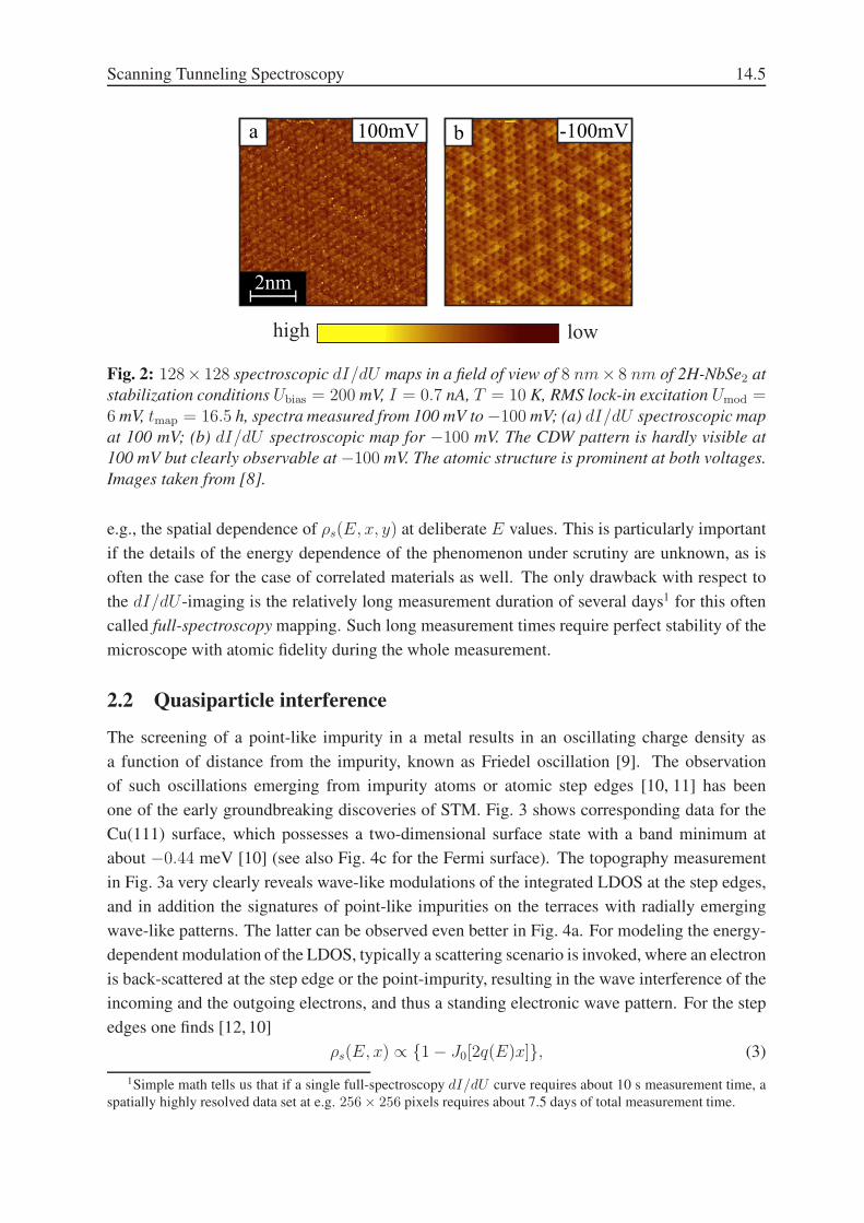
spatial modulations of the LDOS. Fig. 2 shows an example for the spatially dependent LDOS
due to the CDW in 2H-NbSe2 at two selected energies. The data reveal a much stronger impact
of the CDW on the LDOS at Ubias = −100 mV than at Ubias = +100 mV [8].
One way to acquire the data is to measure dI/dU at a fixed Ubias, while scanning a surface
of interest as a function of (x, y). Here, a small modulation voltage Umod is added to Ubias,
and dI/dU |Ubiasis measured directly with a lock-in amplifier. This method (sometimes called
dI/dU-imaging) has the advantage that a spatially highly resolved dI/dU-map can be relatively
quickly recorded together with a topographic map (in the order of minutes to a few hours), thus
posing only moderate constraints on the stability of the used microscope. However, the data
contain dI/dU information only for one specific energy E. Therefore, in order to acquire a
much more comprehensive data set of ρs(E, x, y) at a larger set of energy values, a different
measurement protocol is used: The surface of interest is scanned topographically where the
position of the tip is kept fixed (with feed-back loop switched off) at a grid of (x, y) positions,
and at each of these positions the differential conductance is measured as a function of Ubias.
This technique typically yields a large and comprehensive data set which allows to visualize,
Scanning Tunneling Spectroscopy 14.5
high low
-100mV100mVa b
2nm
Fig. 2: 128× 128 spectroscopic dI/dU maps in a field of view of 8 nm× 8 nm of 2H-NbSe2 at
stabilization conditions Ubias = 200 mV, I = 0.7 nA, T = 10 K, RMS lock-in excitation Umod =6 mV, tmap = 16.5 h, spectra measured from 100 mV to −100 mV; (a) dI/dU spectroscopic map
at 100 mV; (b) dI/dU spectroscopic map for −100 mV. The CDW pattern is hardly visible at
100 mV but clearly observable at −100 mV. The atomic structure is prominent at both voltages.
Images taken from [8].
e.g., the spatial dependence of ρs(E, x, y) at deliberate E values. This is particularly important
if the details of the energy dependence of the phenomenon under scrutiny are unknown, as is
often the case for the case of correlated materials as well. The only drawback with respect to
the dI/dU-imaging is the relatively long measurement duration of several days1 for this often
called full-spectroscopy mapping. Such long measurement times require perfect stability of the
microscope with atomic fidelity during the whole measurement.
2.2 Quasiparticle interference
The screening of a point-like impurity in a metal results in an oscillating charge density as
a function of distance from the impurity, known as Friedel oscillation [9]. The observation
of such oscillations emerging from impurity atoms or atomic step edges [10, 11] has been
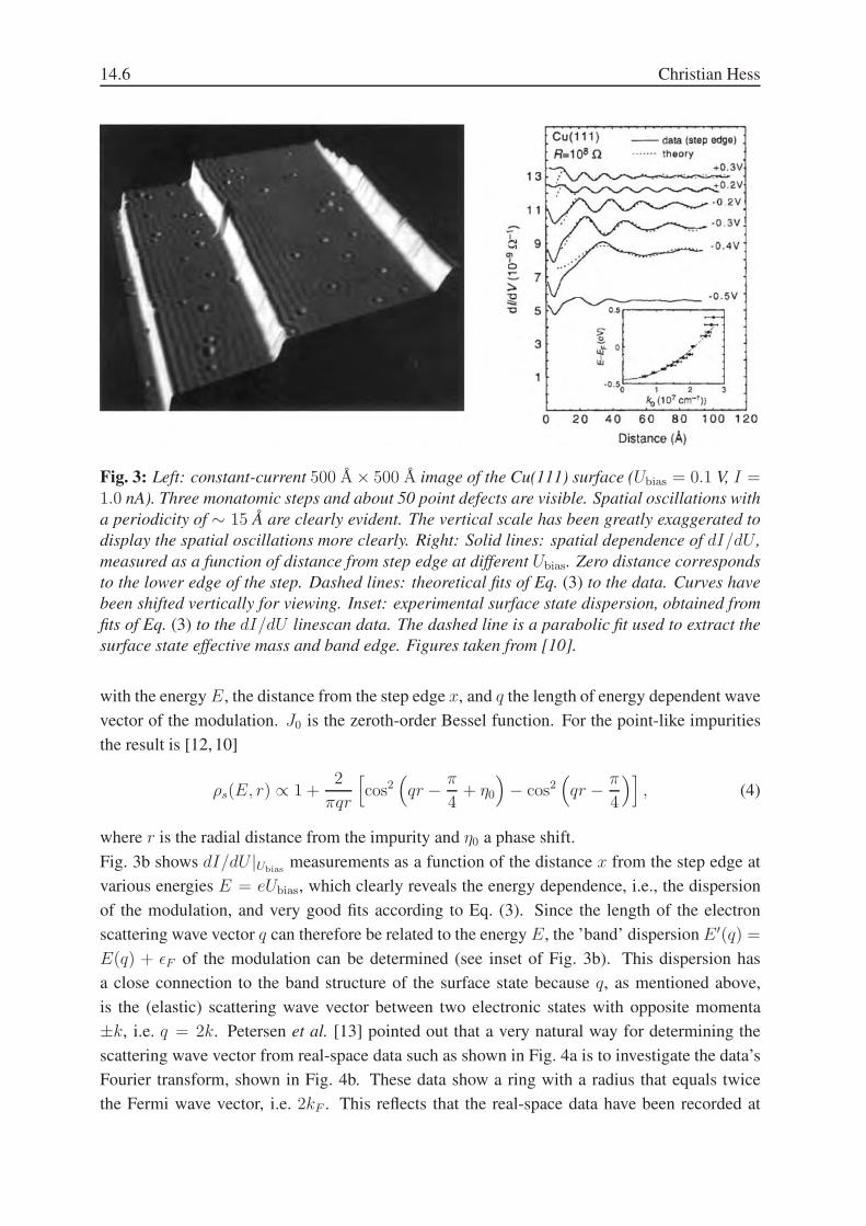
one of the early groundbreaking discoveries of STM. Fig. 3 shows corresponding data for the
Cu(111) surface, which possesses a two-dimensional surface state with a band minimum at
about −0.44 meV [10] (see also Fig. 4c for the Fermi surface). The topography measurement
in Fig. 3a very clearly reveals wave-like modulations of the integrated LDOS at the step edges,
and in addition the signatures of point-like impurities on the terraces with radially emerging
wave-like patterns. The latter can be observed even better in Fig. 4a. For modeling the energy-
dependent modulation of the LDOS, typically a scattering scenario is invoked, where an electron
is back-scattered at the step edge or the point-impurity, resulting in the wave interference of the
incoming and the outgoing electrons, and thus a standing electronic wave pattern. For the step
edges one finds [12, 10]
ρs(E, x) ∝ 1− J0[2q(E)x], (3)
1Simple math tells us that if a single full-spectroscopy dI/dU curve requires about 10 s measurement time, a
spatially highly resolved data set at e.g. 256× 256 pixels requires about 7.5 days of total measurement time.
14.6 Christian Hess
Fig. 3: Left: constant-current 500 A× 500 A image of the Cu(111) surface (Ubias = 0.1 V, I =1.0 nA). Three monatomic steps and about 50 point defects are visible. Spatial oscillations with
a periodicity of ∼ 15 A are clearly evident. The vertical scale has been greatly exaggerated to
display the spatial oscillations more clearly. Right: Solid lines: spatial dependence of dI/dU ,
measured as a function of distance from step edge at different Ubias. Zero distance corresponds
to the lower edge of the step. Dashed lines: theoretical fits of Eq. (3) to the data. Curves have
been shifted vertically for viewing. Inset: experimental surface state dispersion, obtained from
fits of Eq. (3) to the dI/dU linescan data. The dashed line is a parabolic fit used to extract the
surface state effective mass and band edge. Figures taken from [10].
with the energy E, the distance from the step edge x, and q the length of energy dependent wave
vector of the modulation. J0 is the zeroth-order Bessel function. For the point-like impurities
the result is [12, 10]
ρs(E, r) ∝ 1 +2
πqr
[
cos2(
qr −π
4+ η0
)
− cos2(
qr −π
4
)]
, (4)
where r is the radial distance from the impurity and η0 a phase shift.
Fig. 3b shows dI/dU |Ubiasmeasurements as a function of the distance x from the step edge at
various energies E = eUbias, which clearly reveals the energy dependence, i.e., the dispersion
of the modulation, and very good fits according to Eq. (3). Since the length of the electron
scattering wave vector q can therefore be related to the energy E, the ’band’ dispersion E ′(q) =
E(q) + ǫF of the modulation can be determined (see inset of Fig. 3b). This dispersion has
a close connection to the band structure of the surface state because q, as mentioned above,
is the (elastic) scattering wave vector between two electronic states with opposite momenta
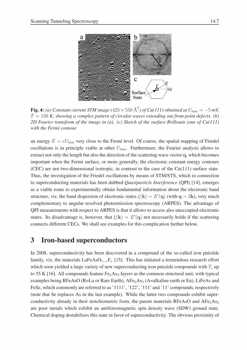
±k, i.e. q = 2k. Petersen et al. [13] pointed out that a very natural way for determining the
scattering wave vector from real-space data such as shown in Fig. 4a is to investigate the data’s
Fourier transform, shown in Fig. 4b. These data show a ring with a radius that equals twice
the Fermi wave vector, i.e. 2kF . This reflects that the real-space data have been recorded at
Scanning Tunneling Spectroscopy 14.7
Fig. 4: (a) Constant current STM image (425×550 A2) of Cu(111) obtained at Ubias = −5 mV,
T = 150 K, showing a complex pattern of circular waves extending out from point defects. (b)
2D Fourier transform of the image in (a). (c) Sketch of the surface Brillouin zone of Cu(111)
with the Fermi contour.
an energy E = eUbias very close to the Fermi level. Of course, the spatial mapping of Friedel
oscillations is in principle viable at other Ubias. Furthermore, the Fourier analysis allows to
extract not only the length but also the direction of the scattering wave vector q, which becomes
important when the Fermi surface, or more generally, the electronic constant energy contours
(CEC) are not two-dimensional isotropic, in contrast to the case of the Cu(111) surface state.
Thus, the investigation of the Friedel oscillations by means of STM/STS, which in connection
to superconducting materials has been dubbed Quasiparticle Interference (QPI) [14], emerges
as a viable route to experimentally obtain fundamental information about the electronic band
structure, viz. the band dispersion of electronic states ξ(k) = E ′(q) (with q = 2k), very much
complementary to angular resolved photoemission spectroscopy (ARPES). The advantage of
QPI measurements with respect to ARPES is that it allows to access also unoccupied electronic
states. Its disadvantage is, however, that ξ(k) = E ′(q) not necessarily holds if the scattering
connects different CECs. We shall see examples for this complication further below.
3 Iron-based superconductors
In 2008, superconductivity has been discovered in a compound of the so-called iron pnictide
family, viz. the materials LaFeAsO1−xFx [15]. This has initiated a tremendous research effort
which soon yielded a large variety of new superconducting iron pnictide compounds with Tc up
to 55 K [16]. All compounds feature Fe2As2-layers as the common structural unit, with typical
examples being RFeAsO (R=La or Rare Earth), AFe2As2 (A=alkaline earth or Eu), LiFeAs and
FeSe, which commonly are referred to as ’1111’, ’122’, ’111’ and ’11’ compounds, respectively
(note that Se replaces As in the last example). While the latter two compounds exhibit super-
conductivity already in their stoichiometric form, the parent materials RFeAsO and AFe2As2
are poor metals which exhibit an antiferromagnetic spin density wave (SDW) ground state.
Chemical doping destabilizes this state in favor of superconductivity. The obvious proximity of
14.8 Christian Hess
superconductivity and antiferromagnetism has lead to the conjecture that superconductivity is
unconventional in these materials in the sense that spin fluctuations are the driving mechanism
of superconductivity with a so-called s±-wave order parameter [17].
STM/STS has been applied to the iron-based superconductors very rapidly after the discovery
of superconductivity. In an initial phase, the experimental work focused on the ’122’-, ’1111’-,
and ’11’-phases, where these pioneering studies revealed very valuable information, including
topographic investigations of the surfaces, the superconducting gap, vortices, and in few cases
even QPI. An essential finding of that period is that for ’122’ and ’1111’ reliable STM/STS
measurements are complicated by either the presence of surface states, as in ’1111’ [18, 19], or
due to a non-trivial cleaving behavior and surface reconstruction in ’122’ [20]. A comprehensive
review of all these works is given in Ref. [21]. The focus will be instead on one particular
material, viz. LiFeAs, for which many of the mentioned difficulties are not an issue, rendering
this compound paradigmatic.
Single crystals of LiFeAs exhibit clean, charge neutral cleaved surfaces [22–26] as we shall
see below, with a bulk-like electronic structure at the surface [27]. LiFeAs is a stoichiometric
superconductor, i.e., superconductivity occurs without any doping, at a relatively high critical
temperature Tc ≈ 18 K [28]. This renders it very different from the canonical ’1111’ and ’122’
iron-arsenide superconductors where the SDW instability is believed to be related to strong
Fermi surface nesting. In the next sections we will discuss how STM/STS can contribute to
revealing more details about the compound’s electronic structure and the superconducting state.
3.1 Gap spectroscopy
Already long time before the invention of the scanning tunneling microscope [29], the pioneer-
ing work of Giaever [30,31] and Rowell et al. [32] on electron tunneling through planar tunnel-
ing junctions with one or two superconducting electrodes provided fundamental insights into
the nature of superconductivity. This concerns the revelation of both the gap in the quasiparticle
tunneling spectrum [30, 31] as well as the signatures of the phonon density in the quasiparticle
DOS of a conventional strong-coupling superconductor [32, 33], which have been understood
as basic supporting evidence of the theories of Bardeen, Cooper and Schrieffer (BCS) [34] and
Eliashberg [35], respectively, showing that the electron-phonon interaction is responsible for
the Cooper pairing in conventional superconductors.
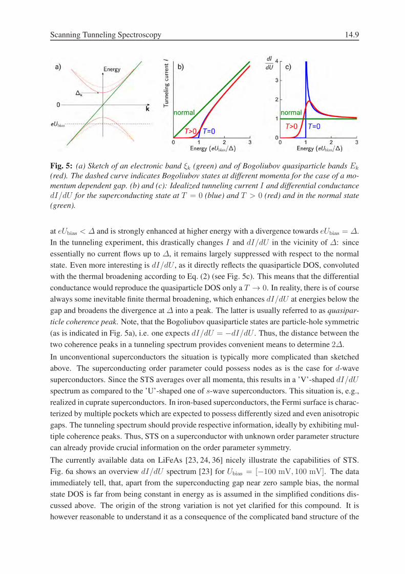
We give a brief reminder of some basic considerations of the superconducting state: Accord-
ing to BCS theory, the Bogoliubov quasiparticle bands Ek are connected to the normal state
electronic bands ξk through E2k = ξ2k + ∆2
k, where ∆k generally is a momentum dependent
energy gap (see Fig. 5a for illustration). For simplicity, we neglect this momentum dependence,
a situation which occurs in purely isotropic s-wave superconductors. If one performs tunneling
spectroscopy on such a superconductor in the normal state (here always with a normal-state tip)
one finds a linear dependence of the tunneling current I of the bias voltage Ubias (see Fig. 5b)
if an idealized energy independent DOS as measured by dI/dU (see Fig. 5c) is present. In the
superconducting state, however, the gap ∆ opens. Hence, the quasiparticle DOS becomes zero
Scanning Tunneling Spectroscopy 14.9
Fig. 5: (a) Sketch of an electronic band ξk (green) and of Bogoliubov quasiparticle bands Ek
(red). The dashed curve indicates Bogoliubov states at different momenta for the case of a mo-
mentum dependent gap. (b) and (c): Idealized tunneling current I and differential conductance
dI/dU for the superconducting state at T = 0 (blue) and T > 0 (red) and in the normal state
(green).
at eUbias < ∆ and is strongly enhanced at higher energy with a divergence towards eUbias = ∆.
In the tunneling experiment, this drastically changes I and dI/dU in the vicinity of ∆: since
essentially no current flows up to ∆, it remains largely suppressed with respect to the normal
state. Even more interesting is dI/dU , as it directly reflects the quasiparticle DOS, convoluted
with the thermal broadening according to Eq. (2) (see Fig. 5c). This means that the differential
conductance would reproduce the quasiparticle DOS only a T → 0. In reality, there is of course
always some inevitable finite thermal broadening, which enhances dI/dU at energies below the
gap and broadens the divergence at ∆ into a peak. The latter is usually referred to as quasipar-
ticle coherence peak. Note, that the Bogoliubov quasiparticle states are particle-hole symmetric
(as is indicated in Fig. 5a), i.e. one expects dI/dU = −dI/dU . Thus, the distance between the
two coherence peaks in a tunneling spectrum provides convenient means to determine 2∆.
In unconventional superconductors the situation is typically more complicated than sketched
above. The superconducting order parameter could possess nodes as is the case for d-wave
superconductors. Since the STS averages over all momenta, this results in a ’V’-shaped dI/dU
spectrum as compared to the ’U’-shaped one of s-wave superconductors. This situation is, e.g.,
realized in cuprate superconductors. In iron-based superconductors, the Fermi surface is charac-
terized by multiple pockets which are expected to possess differently sized and even anisotropic
gaps. The tunneling spectrum should provide respective information, ideally by exhibiting mul-
tiple coherence peaks. Thus, STS on a superconductor with unknown order parameter structure
can already provide crucial information on the order parameter symmetry.
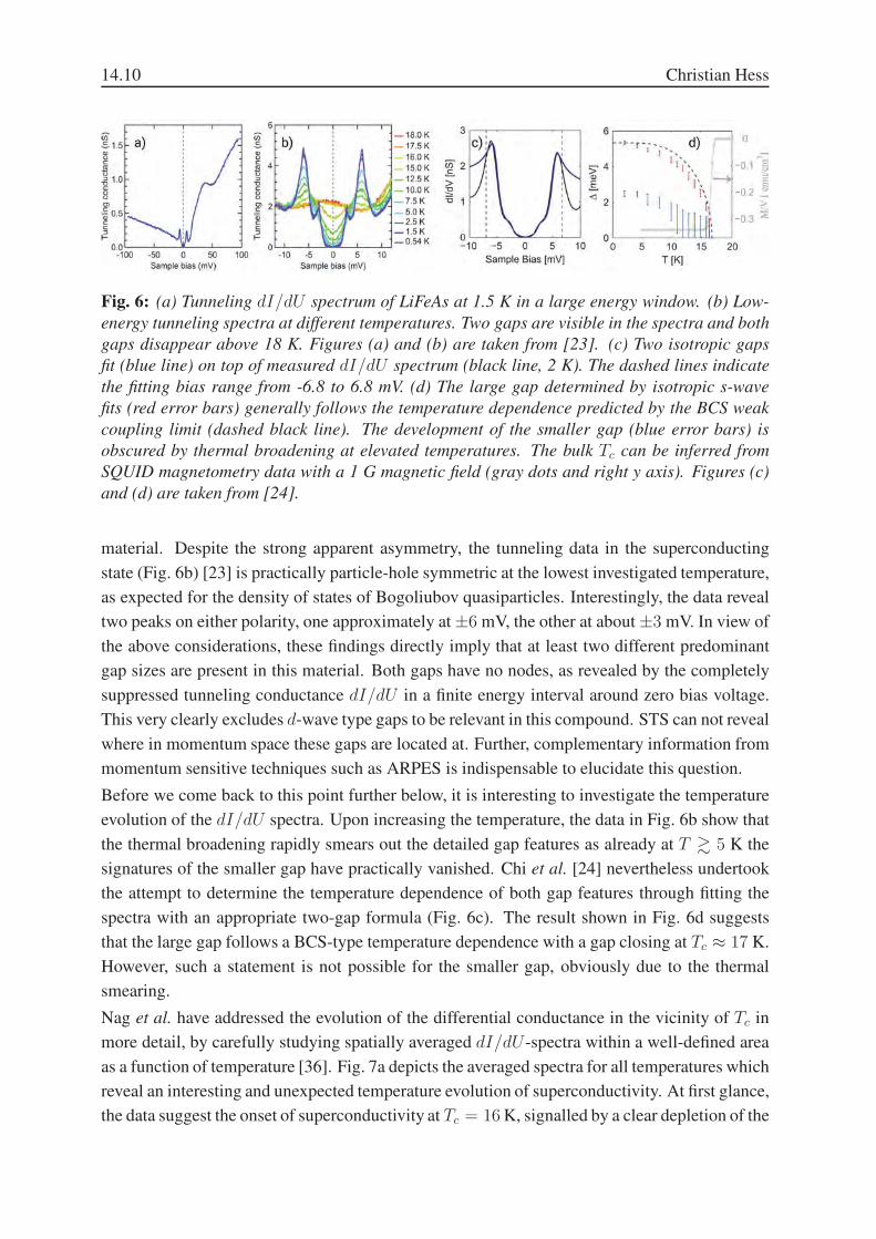
The currently available data on LiFeAs [23, 24, 36] nicely illustrate the capabilities of STS.
Fig. 6a shows an overview dI/dU spectrum [23] for Ubias = [−100 mV, 100 mV]. The data
immediately tell, that, apart from the superconducting gap near zero sample bias, the normal
state DOS is far from being constant in energy as is assumed in the simplified conditions dis-
cussed above. The origin of the strong variation is not yet clarified for this compound. It is
however reasonable to understand it as a consequence of the complicated band structure of the
14.10 Christian Hess
Fig. 6: (a) Tunneling dI/dU spectrum of LiFeAs at 1.5 K in a large energy window. (b) Low-
energy tunneling spectra at different temperatures. Two gaps are visible in the spectra and both
gaps disappear above 18 K. Figures (a) and (b) are taken from [23]. (c) Two isotropic gaps
fit (blue line) on top of measured dI/dU spectrum (black line, 2 K). The dashed lines indicate
the fitting bias range from -6.8 to 6.8 mV. (d) The large gap determined by isotropic s-wave
fits (red error bars) generally follows the temperature dependence predicted by the BCS weak
coupling limit (dashed black line). The development of the smaller gap (blue error bars) is
obscured by thermal broadening at elevated temperatures. The bulk Tc can be inferred from
SQUID magnetometry data with a 1 G magnetic field (gray dots and right y axis). Figures (c)
and (d) are taken from [24].
material. Despite the strong apparent asymmetry, the tunneling data in the superconducting
state (Fig. 6b) [23] is practically particle-hole symmetric at the lowest investigated temperature,
as expected for the density of states of Bogoliubov quasiparticles. Interestingly, the data reveal
two peaks on either polarity, one approximately at ±6 mV, the other at about ±3 mV. In view of
the above considerations, these findings directly imply that at least two different predominant
gap sizes are present in this material. Both gaps have no nodes, as revealed by the completely
suppressed tunneling conductance dI/dU in a finite energy interval around zero bias voltage.
This very clearly excludes d-wave type gaps to be relevant in this compound. STS can not reveal
where in momentum space these gaps are located at. Further, complementary information from
momentum sensitive techniques such as ARPES is indispensable to elucidate this question.
Before we come back to this point further below, it is interesting to investigate the temperature
evolution of the dI/dU spectra. Upon increasing the temperature, the data in Fig. 6b show that
the thermal broadening rapidly smears out the detailed gap features as already at T & 5 K the
signatures of the smaller gap have practically vanished. Chi et al. [24] nevertheless undertook
the attempt to determine the temperature dependence of both gap features through fitting the
spectra with an appropriate two-gap formula (Fig. 6c). The result shown in Fig. 6d suggests
that the large gap follows a BCS-type temperature dependence with a gap closing at Tc ≈ 17 K.
However, such a statement is not possible for the smaller gap, obviously due to the thermal
smearing.
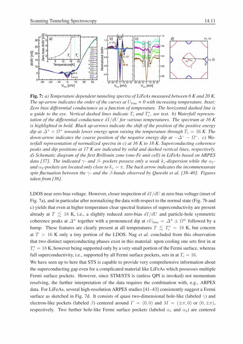
Nag et al. have addressed the evolution of the differential conductance in the vicinity of Tc in
more detail, by carefully studying spatially averaged dI/dU-spectra within a well-defined area
as a function of temperature [36]. Fig. 7a depicts the averaged spectra for all temperatures which
reveal an interesting and unexpected temperature evolution of superconductivity. At first glance,
the data suggest the onset of superconductivity at Tc = 16K, signalled by a clear depletion of the
Scanning Tunneling Spectroscopy 14.11
Fig. 7: a) Temperature dependent tunneling spectra of LiFeAs measured between 6 K and 20 K.
The up-arrow indicates the order of the curves at Ubias = 0 with increasing temperature. Inset:
Zero bias differential conductance as a function of temperature. The horizontal dashed line is
a guide to the eye. Vertical dashed lines indicate Tc and T ∗
c , see text. b) Waterfall represen-
tation of the differential conductance dI/dU for various temperatures. The spectrum at 16 K
is highlighted in bold. Black up-arrows indicate the shift of the position of the positive energy
dip at ∆+ + Ω+ towards lower energy upon raising the temperature through Tc = 16 K. The
down-arrow indicates the coarse position of the negative energy dip at −∆− − Ω−. c) Wa-
terfall representation of normalized spectra in c) at 16 K to 18 K. Superconducting coherence
peaks and dip positions at 17 K are indicated by solid and dashed vertical lines, respectively.
d) Schematic diagram of the first Brillouin zone (one-Fe unit cell) in LiFeAs based on ARPES
data [37]. The indicated γ- and β- pockets possess only a weak kz-dispersion while the α1-
and α2-pockets are located only close to kz = π. The back arrow indicates the incommensurate
spin fluctuation between the γ- and the β-bands observed by Qureshi et al. [38–40]. Figures
taken from [36].
LDOS near zero bias voltage. However, closer inspection of dI/dU at zero bias voltage (inset of
Fig. 7a), and in particular after normalizing the data with respect to the normal state (Fig. 7b and
c) yields that even at higher temperature clear spectral features of superconductivity are present
already at T . 18 K, i.e., a slightly reduced zero-bias dI/dU and particle-hole symmetric
coherence peaks at ∆± together with a pronounced dip at eUbias = ∆± ± Ω± followed by a
hump. These features are clearly present at all temperatures T . T ∗
c = 18 K, but concern
at T > 16 K only a tiny portion of the LDOS. Nag et al. concluded from this observation
that two distinct superconducting phases exist in this material: upon cooling one sets first in at
T ∗
c = 18 K, however being supported only by a very small portion of the Fermi surface, whereas
full superconductivity, i.e., supported by all Fermi surface pockets, sets in at Tc = 16.
We have seen up to here that STS is capable to provide very comprehensive information about
the superconducting gap even for a complicated material like LiFeAs which possesses multiple
Fermi surface pockets. However, since STM/STS is (unless QPI is invoked) not momentum
resolving, the further interpretation of the data requires the combination with, e.g., ARPES
data. For LiFeAs, several high-resolution ARPES studies [41–43] consistently suggest a Fermi
surface as sketched in Fig. 7d. It consists of quasi two-dimensional hole-like (labeled γ) and
electron-like pockets (labeled β) centered around Γ = (0, 0) and M = (±π, 0) or (0,±π),
respectively. Two further hole-like Fermi surface pockets (labeled α1 and α2) are centered
14.12 Christian Hess
Fig. 8: a) Tunneling spectra of LiFeAs taken at the center of vortex (red) and away from vortices
(blue). b) Line profile of tunneling conductance across the vortex center along the nearest Fe-Fe
direction. c) Image of vortices at 1.5 K obtained by mapping the tunneling conductance at ǫF .
The tip was stabilized at Ubias = +20 mV and I = 100 pA. Umod = 0.7 mVrms. Images taken
from [23].
around the Z-point. Since the latter are tiny, Nag et al. [36] concluded these to be natural
candidates for supporting the faint superconductivity at 16 K < T < 18 K. Interestingly, these
pockets have been observed in ARPES to possess the largest superconducting gap ∆α ≈ 6 meV
as compared to ∆γ,β = 3.5 to 4 meV at the γ- and β-pockets [42,43]. With this information the
larger superconducting gap discussed for Fig. 6 can now be assigned to exactly the α-pockets,
whereas the smaller gap is connected to either the γ- or the β-pockets, or both.
There is even more information provided by the dI/dU-spectra, viz. through the dip-hump
structures at eUbias = ∆± ± Ω± in Fig. 7, the signatures of which are already apparent in the
unnormalized spectra shown in Fig. 6b and c. These details have been much debated in terms
of a bosonic mode of energy Ω that couples to the electrons and which should give rise to clear
anomalies in the quasiparticle DOS [35,33]. Chi et al. suggested [24] an antiferromagnetic spin
resonance as the nature of the bosonic mode. In contrast, Nag et al. pointed out [36] that this is
not supported by the temperature independence of Ω, which in case of the dip being connected
to an antiferromagnetic resonance should track the temperature dependence of order parameter,
and the de facto absence of an antiferromagnetic resonance in inelastic neutron scattering results
on LiFeAs [38,39]. It is interesting to note that recent theoretical work [44] suggested inelastic
tunneling processes to play a very important role in the interpretation of the dip-hump feature.
3.1.1 Vortex spectroscopy
In the above considerations, the spatial dependence of the superconducting state did not play
a role, i.e., the particular strength of STM/STS to spatially resolve electronic structure has not
been exploited. This is in order as long as the material exhibits a spatially homogeneous super-
conducting state, which is often the case. A very obvious situation where the superconducting
state is spatially inhomogeneous is the Shubnikov phase of a type-II superconductor, where
magnetic flux lines (vortices) enter the superconducting volume. Each flux line holds one mag-
Scanning Tunneling Spectroscopy 14.13
highlow
5 nm
a
highlow
5 nm
a b
-40 -20 0 20 400
5
10
15
20
dI/
dV
(nS
)
sample bias (mV)
Fig. 9: (a) Surface topography of LiFeAs measured in constant current mode (I = 600 pA,
Vbias = −50 mV) taken at T ≈ 5.8 K. Black arrows indicate the direction of the lattice constants
[28] with a = 3.7914 A. (b) Spatially averaged tunneling spectrum taken in the square area
(dashed lines) in (a). The spectrum exhibits a gap with 2∆ ∼ 10 mV, which (taking thermal
broadening into account) is consistent with low-temperature (∼ 500 mK) tunneling data in
Fig. 6 of the superconducting gap of LiFeAs. Representative energy values for further QPI
analysis in Fig. 10 are marked by red circles. Figure taken from [22].
netic flux quantum φ0 = h/(2e). The magnetic field is maximum inside the vortex core and
then radially decays on a length scale given by the London penetration depth λL. At the same
time, the superconducting wave function decays from outside towards zero at the vortex core
with the Ginzburg-Landau coherence length ξGL as the determining length scale. This has a
strong impact on the LDOS measured at the vortex core, because it should be enhanced at en-
ergy values inside the superconducting gap with respect to the superconducting LDOS. This is
indeed the case also for LiFeAs as is shown in Figure 8. Hanaguri et al. [23] report a complete
suppression of the both sets of coherence peaks in favor of pronounced and asymmetric vortex
core states inside the gap (Fig. 8a). Fig. 8b shows the spatial evolution of the spectrum along
the Fe-Fe direction. In principle, one can expect interesting information about the nature of the
superconducting order parameter from such spatial studies. However, it has been pointed out by
Wang et al. [45] that it is a priori difficult to disentangle the effect of order parameter symmetry
from anisotropy effects of the Fermi surface.
The enhanced LDOS at the vortex core leads to an enhanced value of the differential conduc-
tance dI/dU and thus can be used to visualize the structure of the vortex lattice as is exemplified
in Fig. 8c. The investigation of such vortex matter is a separate field as such. The interested
reader is referred to the original literature [23, 45] and references therein.
3.2 Quasiparticle interference
In the following we begin by largely following the first experimental paper on the QPI of
LiFeAs [22]. Afterwards, we compare and discuss the earlier findings with more recent pub-
lications [26, 46, 47]. Prior to performing QPI measurements it is important to have a good
account on the surface to be investigated which can be achieved by topographic STM mea-
14.14 Christian Hess
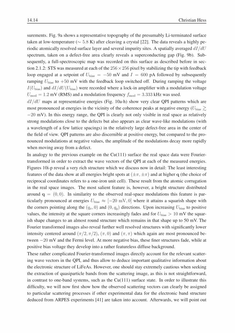
surements. Fig. 9a shows a representative topography of the presumably Li-terminated surface
taken at low-temperature (∼ 5.8 K) after cleaving a crystal [22]. The data reveals a highly pe-
riodic atomically resolved surface layer and several impurity sites. A spatially averaged dI/dU
spectrum, taken on a defect-free area clearly reveals a superconducting gap (Fig. 9b). Sub-
sequently, a full-spectroscopic map was recorded on this surface as described before in sec-
tion 2.1.2: STS was measured at each of the 256×256 pixel by stabilizing the tip with feedback
loop engaged at a setpoint of Ubias = −50 mV and I = 600 pA followed by subsequently
ramping Ubias to +50 mV with the feedback loop switched off. During ramping the voltage
I(Ubias) and dI/dU(Ubias) were recorded where a lock-in amplifier with a modulation voltage
Umod = 1.2 mV (RMS) and a modulation frequency fmod = 3.333 kHz was used.
dI/dU maps at representative energies (Fig. 10a-h) show very clear QPI patterns which are
most pronounced at energies in the vicinity of the coherence peaks at negative energy (Ubias &
−20 mV). In this energy range, the QPI is clearly not only visible in real space as relatively
strong modulations close to the defects but also appears as clear wave-like modulations (with
a wavelength of a few lattice spacings) in the relatively large defect-free area in the center of
the field of view. QPI patterns are also discernible at positive energy, but compared to the pro-
nounced modulations at negative values, the amplitude of the modulations decay more rapidly
when moving away from a defect.
In analogy to the previous example on the Cu(111) surface the real space data were Fourier-
transformed in order to extract the wave vectors of the QPI at each of the measured energies.
Figures 10i-p reveal a very rich structure which we discuss now in detail: The least interesting
features of the data show at all energies bright spots at (±π,±π) and at higher q (the choice of
reciprocal coordinates refers to a one-iron unit cell). These result from the atomic corrugation
in the real space images. The most salient feature is, however, a bright structure distributed
around q = (0, 0). In similarity to the observed real-space modulations this feature is par-
ticularly pronounced at energies Ubias ≈ [−20 mV, 0] where it attains a squarish shape with
the corners pointing along the (qx, 0) and (0, qy) directions. Upon increasing Ubias to positive
values, the intensity at the square corners increasingly fades and for Ubias > 10 mV the squar-
ish shape changes to an almost round structure which remains in that shape up to 50 mV. The
Fourier transformed images also reveal further well resolved structures with significantly lower
intensity centered around (π/2, π/2), (π, 0) and (π, π) which again are most pronounced be-
tween −20 mV and the Fermi level. At more negative bias, these finer structures fade, while at
positive bias voltage they develop into a rather featureless diffuse background.
These rather complicated Fourier-transformed images directly account for the relevant scatter-
ing wave vectors in the QPI, and thus allow to deduce important qualitative information about
the electronic structure of LiFeAs. However, one should stay extremely cautious when seeking
the extraction of quasiparticle bands from the scattering image, as this is not straightforward,
in contrast to one-band systems, such as the Cu(111) surface state. In order to illustrate this
difficulty, we will now first show how the observed scattering vectors can clearly be assigned
to particular scattering processes if other experimental data for the electronic band structure
deduced from ARPES experiments [41] are taken into account. Afterwards, we will point out
Scanning Tunneling Spectroscopy 14.15
a
-31.2 mV
b
-23.8 mV
c
-14.1 mV
d
-11.7 mV
e
-6.8 mV
f
-1.9 mV
g
+10.3 mV
h
+28.6 mV
high
low
p
+28.6 mV
i
-31.2 mV
-1.9 mV
o
+10.3 mV-2p
2p
j
-23.8 mV
k
-14.1 mV
l
-11.7 mV
high
low
-2p 0
0
m
-6.8 mV
2p
5 nm
n
Fig. 10: (a-h) SI-STM maps of the region shown in Fig. 9 at selected representative bias volt-
ages. (i-p) Fourier transformed images of the maps shown in a-h. Bright spots at (±π,±π) and
at higher q result from the atomic corrugation in the real space images. Figure taken from [22].
an alternative interpretation of the data [26], which, however, is not compatible with the com-
pound’s electronic structure.
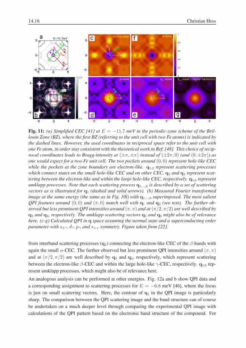
Fig. 11a and b compare the CEC of LiFeAs at E = −11.7 mV derived from ARPES data [41]
with the observed QPI intensities in the Fourier transformed image. Most prominent is that the
observed central squarish structure in Figure 11b appears like a somewhat enlarged smeared
replica of the large, hole-like CEC of the γ-band around (0, 0). This observation can directly
be understood as stemming from interband scattering processes (q1) connecting the very small
CEC of the α-bands2 and the larger squarish-shaped γ-CEC around (0, 0). Furthermore, the
much weaker structure at q = (π, 0) in Fig. 11b apparently can be rationalized as stemming
2For simplicity we do not distinguish between the α1 and α2-bands.
14.16 Christian Hess
Fig. 11: (a) Simplified CEC [41] at E = −11.7 meV in the periodic-zone scheme of the Bril-
louin Zone (BZ), where the first BZ (referring to the unit cell with two Fe atoms) is indicated by
the dashed lines. However, the used coordinates in reciprocal space refer to the unit cell with
one Fe atom, in order stay consistent with the theoretical work in Ref. [48]. This choice of recip-
rocal coordinates leads to Bragg-intensity at (±π,±π) instead of (±2π, 0) (and (0,±2π)) as
one would expect for a two-Fe unit cell. The two pockets around (0, 0) represent hole-like CEC
while the pockets at the zone boundary are electron-like. q1,2 represent scattering processes
which connect states on the small hole-like CEC and on other CEC, q3 and q4 represent scat-
tering between the electron-like and within the large hole-like CEC, respectively. q5,6 represent
umklapp processes. Note that each scattering process q1,...,6 is described by a set of scattering
vectors as is illustrated for q1 (dashed and solid arrows). (b) Measured Fourier transformed
image at the same energy (the same as in Fig. 10l) with q1,...,6 superimposed. The most salient
QPI features around (0, 0) and (π, 0) match well with q1 and q2 (see text). The further ob-
served but less prominent QPI intensities around (π, π) and at (π/2, π/2) are well described by
q3 and q4, respectively. The umklapp scattering vectors q5 and q6 might also be of relevance
here. (c-g) Calculated QPI in q space assuming the normal state and a superconducting order
parameter with s±-, d-, p-, and s++ symmetry. Figure taken from [22].
from interband scattering processes (q2) connecting the electron-like CEC of the β-bands with
again the small α-CEC. The further observed but less prominent QPI intensities around (π, π)
and at (π/2, π/2) are well described by q3 and q4, respectively, which represent scattering
between the electron-like β-CEC and within the large hole-like γ-CEC, respectively. q5,6 rep-
resent umklapp processes, which might also be of relevance here.
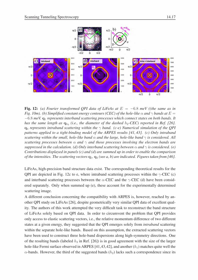
An analogous analysis can be performed at other energies. Fig. 12a and b show QPI data and
a corresponding assignment to scattering processes for E = −6.8 meV [46], where the focus
is just on small scattering vectors. Here, the contour of q1 in the QPI image is particularly
sharp. The comparison between the QPI scattering image and the band structure can of course
be undertaken on a much deeper level through comparing the experimental QPI image with
calculations of the QPI pattern based on the electronic band structure of the compound. For
Scanning Tunneling Spectroscopy 14.17
Fig. 12: (a) Fourier transformed QPI data of LiFeAs at E = −6.8 meV ((the same as in
Fig. 10m). (b) Simplified constant energy contours (CEC) of the hole-like α and γ bands at E =−6.8 meV. q1 represents interband scattering processes which connect states on both bands. It
has the same length as qh2(i.e., the diameter of the dashed h2-CEC) reported in Ref. [26].
q4 represents intraband scattering within the γ band. (c-e) Numerical simulation of the QPI
patterns applied to a tight-binding model of the ARPES results [41, 43]. (c) Only intraband
scattering within the small, hole-like band α and the large, hole-like band γ is considered. All
scattering processes between α and γ and those processes involving the electron bands are
suppressed in the calculation. (d) Only interband scattering between α and γ is considered. (e)
Contributions displayed in panels (c) and (d) are summed up in order to enable the comparison
of the intensities. The scattering vectors q1, q4 (see a, b) are indicated. Figures taken from [46].
LiFeAs, high-precision band structure data exist. The corresponding theoretical results for the
QPI are depicted in Fig. 12c to e, where intraband scattering processes within the γ-CEC (c)
and interband scattering processes between the α-CEC and the γ-CEC (d) have been consid-
ered separately. Only when summed up (e), these account for the experimentally determined
scattering image.
A different conclusion concerning the compatibility with ARPES is, however, reached by an-
other QPI study on LiFeAs [26], despite geometrically very similar QPI data of excellent qual-
ity. The authors of this work attempted the very difficult task to reconstruct the band structure
of LiFeAs solely based on QPI data. In order to circumvent the problem that QPI provides
only access to elastic scattering vectors, i.e., the relative momentum difference of two different
states at a given energy, they suggested that the QPI emerges solely from intraband scattering
within the separate hole-like bands. Based on this assumption, the extracted scattering vectors
have been used to construct three hole-band dispersions along high-symmetry directions. One
of the resulting bands (labeled h3 in Ref. [26]) is in good agreement with the size of the larger
hole-like Fermi surface observed in ARPES [41,43,42], and another (h1) matches quite well the
α-bands. However, the third of the suggested bands (h2) lacks such a correspondence since its
14.18 Christian Hess
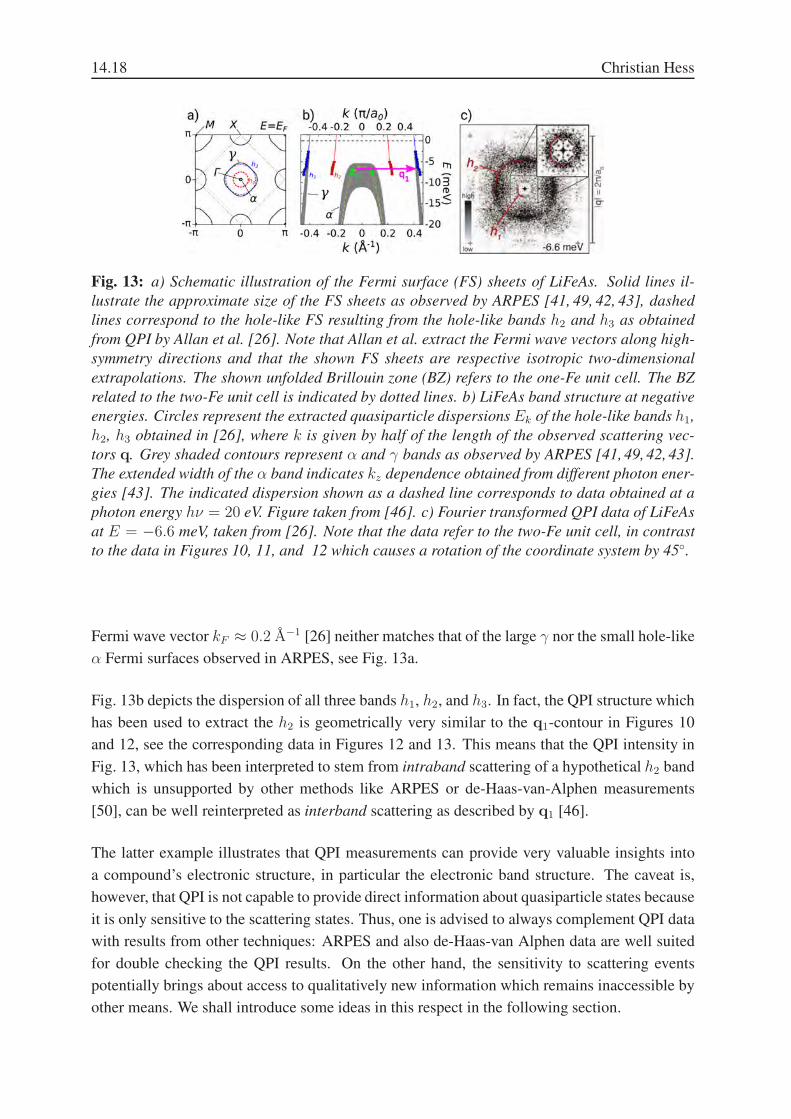
Fig. 13: a) Schematic illustration of the Fermi surface (FS) sheets of LiFeAs. Solid lines il-
lustrate the approximate size of the FS sheets as observed by ARPES [41, 49, 42, 43], dashed
lines correspond to the hole-like FS resulting from the hole-like bands h2 and h3 as obtained
from QPI by Allan et al. [26]. Note that Allan et al. extract the Fermi wave vectors along high-
symmetry directions and that the shown FS sheets are respective isotropic two-dimensional
extrapolations. The shown unfolded Brillouin zone (BZ) refers to the one-Fe unit cell. The BZ
related to the two-Fe unit cell is indicated by dotted lines. b) LiFeAs band structure at negative
energies. Circles represent the extracted quasiparticle dispersions Ek of the hole-like bands h1,
h2, h3 obtained in [26], where k is given by half of the length of the observed scattering vec-
tors q. Grey shaded contours represent α and γ bands as observed by ARPES [41, 49, 42, 43].
The extended width of the α band indicates kz dependence obtained from different photon ener-
gies [43]. The indicated dispersion shown as a dashed line corresponds to data obtained at a
photon energy hν = 20 eV. Figure taken from [46]. c) Fourier transformed QPI data of LiFeAs
at E = −6.6 meV, taken from [26]. Note that the data refer to the two-Fe unit cell, in contrast
to the data in Figures 10, 11, and 12 which causes a rotation of the coordinate system by 45.
Fermi wave vector kF ≈ 0.2 A−1 [26] neither matches that of the large γ nor the small hole-like
α Fermi surfaces observed in ARPES, see Fig. 13a.
Fig. 13b depicts the dispersion of all three bands h1, h2, and h3. In fact, the QPI structure which
has been used to extract the h2 is geometrically very similar to the q1-contour in Figures 10
and 12, see the corresponding data in Figures 12 and 13. This means that the QPI intensity in
Fig. 13, which has been interpreted to stem from intraband scattering of a hypothetical h2 band
which is unsupported by other methods like ARPES or de-Haas-van-Alphen measurements
[50], can be well reinterpreted as interband scattering as described by q1 [46].
The latter example illustrates that QPI measurements can provide very valuable insights into
a compound’s electronic structure, in particular the electronic band structure. The caveat is,
however, that QPI is not capable to provide direct information about quasiparticle states because
it is only sensitive to the scattering states. Thus, one is advised to always complement QPI data
with results from other techniques: ARPES and also de-Haas-van Alphen data are well suited
for double checking the QPI results. On the other hand, the sensitivity to scattering events
potentially brings about access to qualitatively new information which remains inaccessible by
other means. We shall introduce some ideas in this respect in the following section.
Scanning Tunneling Spectroscopy 14.19
Fig. 14: (a) A simplified two-band model for the pnictides with a hole-like band centered at
k = (0, 0) and an electron-like band centered at k = (π/a, π/a). (b) The Fermi surfaces
of the bands in (a). The vectors qh-h and qe-e show intraband scattering within the hole and
electron pockets, respectively, while qh-e shows interband scattering between the two. In the
s± scenario ∆k switches sign between the initial and final states of the qh-e scattering process,
while it remains the same in the s++ scenario. Image taken from [47]. (c) A summary of the
QPI selection rules expected for a pnictide superconductor with s++ or s±. The QPI intensity
of a scattering vector is either suppressed or enhanced inside the superconducting gap relative
to the intensity outside the gap. The intensity variations stem from the energy dependence of the
coherence factors. The four combinations of two pairing symmetries and two kinds of impurities
result in four distinct sets of selection rules. Table taken from [47].
3.2.1 Accessing the structure of the superconducting order parameter
In the superconducting state the DOS is redistributed by the opening of the superconducting
gap. More specifically, in the superconducting state the DOS at energy-values close to the gap
value is further boosted in comparison to the normal state since the quasiparticle dispersion
Ek = ±(ξ2k+ |∆k|
2)1/2 is rather flat (see Fig. 5a). Furthermore, depending on the gap function
∆k, particular scattering channels are suppressed while others are enhanced according to the co-
herence factors of the superconducting state. Consequently, the QPI measured at energies |E|
close to the averaged gap value will be redistributed, thereby containing detailed information
about the structure of the superconducting order parameter. More specifically, the scattering
rate between quasiparticle states with momenta k and k′ is proportional to coherence factors
(uku∗
k′ ∓ vkv∗
k′), where the ∓ sign is determined by the magnetic/non-magnetic nature of the
underlying scattering mechanism. The coherence factors are sensitive to the phase of the super-
conducting order parameter via the Bogoliubov coefficients uk and vk which fulfil the relation
vk/uk = (Ek − ξk)/∆∗
kwith the quasiparticle energy Ek = ±(ξ2
k+ |∆k|
2)1/2 [34, 51]. Thus,
through the coherence factors, the QPI pattern is in principle decisively influenced by the nature
of superconductivity, in particular the symmetry of the superconducting gap. Pioneering studies
which involve the analysis of QPI data along these lines have been performed on cuprate high-
temperature superconductors [52] and, more recently, also for iron-based superconductors [53].
Here, we summarize briefly the currently available results for LiFeAs.
In order to exploit the phase sensitivity of the QPI, Hanke et al. [22] calculated the QPI in the su-
perconducting state using an appropriate BCS model for LiFeAs which can describe three cases
of elementary singlet pairing (s++, s±, and d-wave) as well as a p-wave triplet pairing scenario.
These calculations were based on a band structure model matching the ARPES results [41] (see
14.20 Christian Hess
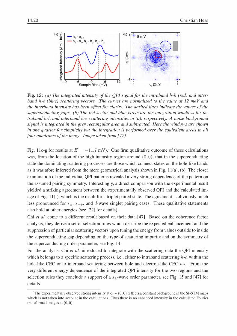
Fig. 15: (a) The integrated intensity of the QPI signal for the intraband h-h (red) and inter-
band h-e (blue) scattering vectors. The curves are normalized to the value at 12 meV and
the interband intensity has been offset for clarity. The dashed lines indicate the values of the
superconducting gaps. (b) The red sector and blue circle are the integration windows for in-
traband h-h and interband h-e scattering intensities in (a), respectively. A noise background
signal is integrated in the grey rectangular area and subtracted. Here the windows are shown
in one quarter for simplicity but the integration is performed over the equivalent areas in all
four quadrants of the image. Image taken from [47].
Fig. 11c-g for results at E = −11.7 mV).3 One firm qualitative outcome of these calculations
was, from the location of the high intensity region around (0, 0), that in the superconducting
state the dominating scattering processes are those which connect states on the hole-like bands
as it was afore inferred from the mere geometrical analysis shown in Fig. 11(a), (b). The closer
examination of the individual QPI patterns revealed a very strong dependence of the pattern on
the assumed pairing symmetry. Interestingly, a direct comparison with the experimental result
yielded a striking agreement between the experimentally observed QPI and the calculated im-
age of Fig. 11(f), which is the result for a triplet paired state. The agreement is obviously much
less pronounced for s±, s++, and d-wave singlet pairing cases. These qualitative statements
also hold at other energies (see [22] for details).
Chi et al. come to a different result based on their data [47]. Based on the coherence factor
analysis, they derive a set of selection rules which describe the expected enhancement and the
suppression of particular scattering vectors upon tuning the energy from values outside to inside
the superconducting gap depending on the type of scattering impurity and on the symmetry of
the superconducting order parameter, see Fig. 14.
For the analysis, Chi et al. introduced to integrate with the scattering data the QPI intensity
which belongs to a specific scattering process, i.e., either to intraband scattering h-h within the
hole-like CEC or to interband scattering between hole and electron-like CEC h-e. From the
very different energy dependence of the integrated QPI intensity for the two regions and the
selection rules they conclude a support of a s±-wave order parameter, see Fig. 15 and [47] for
details.
3The experimentally observed strong intensity at q ∼ (0, 0) reflects a constant background in the SI-STM maps
which is not taken into account in the calculations. Thus there is no enhanced intensity in the calculated Fourier
transformed images at (0, 0).
Scanning Tunneling Spectroscopy 14.21
It is worth pointing out that these unsatisfactory conflicting results [22, 47] provide the moti-
vation for ongoing research. Hirschfeld et al. have theoretically addressed this problem [54]
and suggested to use the temperature dependence of momentum-integrated QPI data in order to
give a firm statement on the superconducting gap structure. Experimentally, this is, however,
still open.
4 Cuprate superconductors
There exists vast literature which provides excellent introduction to the physics of the cuprate
superconductors, see e.g. [55]. What we need to know here is that the electronic phase diagram
of hole-doped cuprates has much resemblance to that of the canonical 122 or 1111 iron-based
superconductors. One important difference is that the undoped parent state is an antiferromag-
netic (charge transfer) insulator. Charge-doping causes its destruction and the emergence of
superconductivity with the highest critical temperature Tc known so far (up to ∼ 135 K) for
ambient pressure conditions [55]. The hole-like Fermi surface consists only of one band (which
renders the situation in QPI investigations much simpler as compared to the iron-based super-
conductors), with a d-wave order parameter in the superconducting state with nodes on the
Fermi surface along the (±π,±π) directions.
4.1 Quasiparticle interference and the octet-model
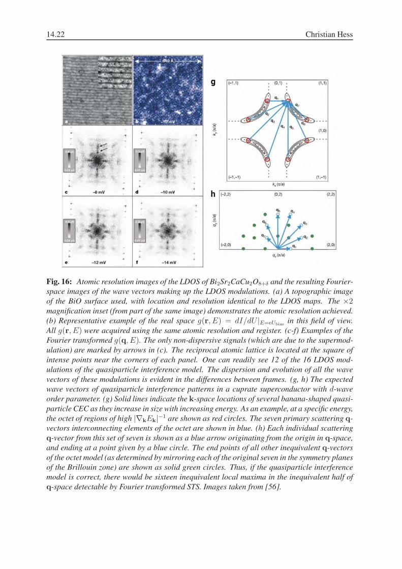
In fact, the modern investigation of QPI analysis has first been introduced in pioneering work
on the cuprate superconductors [14, 56, 57]. Fig. 16 shows representative experimental data for
the material Bi2Sr2CaCu2O8+δ [56]. The topographic data in Fig. 16a reveal the characteristic
BiO-terminated surface of Bi2Sr2CaCu2O8+δ which exhibits a stripe-like periodic superstruc-
ture. Full dI/dU spectroscopic mapping of the same field of view reveals pronounced QPI
signatures; representative real space and Fourier transformed data are shown in Figures 16b
and (c-f), respectively. The latter reveal multiple high-intensity spots which possess a clear
energy dispersion. It has been proposed by McElroy et al. [56] that these spots result from
quasiparticle scattering between eight specific points in momentum space which emerge in the
superconducting state. The situation is illustrated in Fig. 16g which shows ’banana’-shaped
quasiparticle CEC which emerge at energies smaller than the maximum |∆k| in the supercon-
ducting d-wave state. McElroy et al. argued [56] that since the quasiparticle DOS ρs at a given
energy Ek = ω is proportional to
∫
Ek=ω
|∇kEk|−1 dk, (5)
the primary contributions to ρs(ω) stem from the two tips of the ’banana’ where |∇kEk|−1
is largest, and thus the QPI should be dominated by the seven scattering vectors q1...7 which
connect the eight ’banana’ tips (see Fig. 16g and h). This model has proven to describe the
14.22 Christian Hess
Fig. 16: Atomic resolution images of the LDOS of Bi2Sr2CaCu2O8+δ and the resulting Fourier-
space images of the wave vectors making up the LDOS modulations. (a) A topographic image
of the BiO surface used, with location and resolution identical to the LDOS maps. The ×2magnification inset (from part of the same image) demonstrates the atomic resolution achieved.
(b) Representative example of the real space g(r, E) = dI/dU |E=eUbiasin this field of view.
All g(r, E) were acquired using the same atomic resolution and register. (c-f) Examples of the
Fourier transformed g(q, E). The only non-dispersive signals (which are due to the supermod-
ulation) are marked by arrows in (c). The reciprocal atomic lattice is located at the square of
intense points near the corners of each panel. One can readily see 12 of the 16 LDOS mod-
ulations of the quasiparticle interference model. The dispersion and evolution of all the wave
vectors of these modulations is evident in the differences between frames. (g, h) The expected
wave vectors of quasiparticle interference patterns in a cuprate superconductor with d-wave
order parameter. (g) Solid lines indicate the k-space locations of several banana-shaped quasi-
particle CEC as they increase in size with increasing energy. As an example, at a specific energy,
the octet of regions of high |∇kEk|−1 are shown as red circles. The seven primary scattering q-
vectors interconnecting elements of the octet are shown in blue. (h) Each individual scattering
q-vector from this set of seven is shown as a blue arrow originating from the origin in q-space,
and ending at a point given by a blue circle. The end points of all other inequivalent q-vectors
of the octet model (as determined by mirroring each of the original seven in the symmetry planes
of the Brillouin zone) are shown as solid green circles. Thus, if the quasiparticle interference
model is correct, there would be sixteen inequivalent local maxima in the inequivalent half of
q-space detectable by Fourier transformed STS. Images taken from [56].
Scanning Tunneling Spectroscopy 14.23
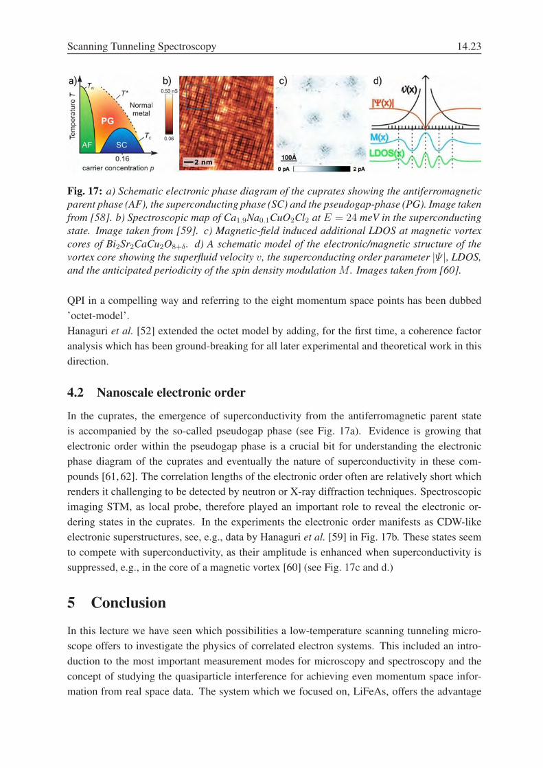
Fig. 17: a) Schematic electronic phase diagram of the cuprates showing the antiferromagnetic
parent phase (AF), the superconducting phase (SC) and the pseudogap-phase (PG). Image taken
from [58]. b) Spectroscopic map of Ca1.9Na0.1CuO2Cl2 at E = 24 meV in the superconducting
state. Image taken from [59]. c) Magnetic-field induced additional LDOS at magnetic vortex
cores of Bi2Sr2CaCu2O8+δ. d) A schematic model of the electronic/magnetic structure of the
vortex core showing the superfluid velocity v, the superconducting order parameter |Ψ |, LDOS,
and the anticipated periodicity of the spin density modulation M . Images taken from [60].
QPI in a compelling way and referring to the eight momentum space points has been dubbed
’octet-model’.
Hanaguri et al. [52] extended the octet model by adding, for the first time, a coherence factor
analysis which has been ground-breaking for all later experimental and theoretical work in this
direction.
4.2 Nanoscale electronic order
In the cuprates, the emergence of superconductivity from the antiferromagnetic parent state
is accompanied by the so-called pseudogap phase (see Fig. 17a). Evidence is growing that
electronic order within the pseudogap phase is a crucial bit for understanding the electronic
phase diagram of the cuprates and eventually the nature of superconductivity in these com-
pounds [61, 62]. The correlation lengths of the electronic order often are relatively short which
renders it challenging to be detected by neutron or X-ray diffraction techniques. Spectroscopic
imaging STM, as local probe, therefore played an important role to reveal the electronic or-
dering states in the cuprates. In the experiments the electronic order manifests as CDW-like
electronic superstructures, see, e.g., data by Hanaguri et al. [59] in Fig. 17b. These states seem
to compete with superconductivity, as their amplitude is enhanced when superconductivity is
suppressed, e.g., in the core of a magnetic vortex [60] (see Fig. 17c and d.)
5 Conclusion
In this lecture we have seen which possibilities a low-temperature scanning tunneling micro-
scope offers to investigate the physics of correlated electron systems. This included an intro-
duction to the most important measurement modes for microscopy and spectroscopy and the
concept of studying the quasiparticle interference for achieving even momentum space infor-
mation from real space data. The system which we focused on, LiFeAs, offers the advantage
14.24 Christian Hess
that clean experimental data exist that allow to discuss many different aspects of scanning tun-
neling spectroscopy and the different types of information that can be gained. Further aspects
of scanning tunneling spectroscopy of correlated materials were introduced through briefly dis-
cussing important work on cuprate superconductors. Thus, this lecture, together with the given
literature, should provide the necessary basis for understanding the work on different systems
such as the heavy fermion systems or non-superconducting transition-metal compounds.
It should be noted that the electronic ordering states which are ubiquitous in correlated electron
systems in principle are expected to be accompanied by a spin density wave, as is indicated
in Fig. 17d. This magnetic superstructure has not yet been observed by STM/STS because
this techniques a priori is not sensitive to magnetism. This changes, however, if a magnetic
tunneling tip is used, a technique which has been explored and brought into maturity for non- or
weakly correlated systems [63]. The experimental efforts to apply this spin-polarized scanning
tunneling microscopy (SP-STM) to correlated electron systems have just started, yielding first
exciting results [64]. One may stay tuned.
Scanning Tunneling Spectroscopy 14.25
References
[1] J. Bardeen, Phys. Rev. Lett. 6, 57 (1961)
[2] J. Tersoff and D.R. Hamann, Phys. Rev. Lett. 50, 1998 (1983)
[3] J. Tersoff and D.R. Hamann, Phys. Rev. B 31, 805 (1985)
[4] J.A. Strocio and W.J. Kaiser (Eds.): Scanning Tunneling Microscopy
(Academic Press, Inc., 1993)
[5] R. Wiesendanger: Scanning Probe Microscopy and Spectroscopy
Methods and Applications (Cambridge University Press, 1994)
[6] D.E. Moncton, J.D. Axe, and F.J. DiSalvo, Phys. Rev. Lett. 34, 734 (1975)
[7] B.E. Brown and D.J. Beerntsen, Acta Crystallographica 18, 31 (1965)
[8] R. Schlegel, T. Hanke, D. Baumann, M. Kaiser, P.K. Nag, R. Voigtlander, D. Lindackers,
B. Buchner, and C. Hess, Review of Scientific Instruments 85, 013706 (2014)
[9] J. Ziman: Principles of the Theory of Solids (Cambridge University Press, 1972)
[10] M.F. Crommie, C.P. Lutz, and D.M. Eigler, Nature 363, 524 (1993)
[11] Y. Hasegawa and P. Avouris, Phys. Rev. Lett. 71, 1071 (1993)
[12] P. Avouris, I. Lyo, R.E. Walkup, and Y. Hasegawa,
Journal of Vacuum Science & Technology B 12, 1447 (1994)
[13] L. Petersen, P.T. Sprunger, P. Hofmann, E. Lægsgaard, B.G. Briner, M. Doering,
H.-P. Rust, A.M. Bradshaw, F. Besenbacher, and E.W. Plummer,
Phys. Rev. B 57, R6858 (1998)
[14] J.E. Hoffman, K. McElroy, D.-H. Lee, K.M. Lang, H. Eisaki, S. Uchida, and J.C. Davis,
Science 297, 1148 (2002)
[15] Y. Kamihara, T. Watanabe, M. Hirano, and H. Hosono,
J. Am. Chem. Soc. 130, 3296 (2008)
[16] D.C. Johnston, Advances in Physics 59, 803 (2010)
[17] I.I. Mazin, D.J. Singh, M.D. Johannes, and M.H. Du, Phys. Rev. Lett. 101, 057003 (2008)
[18] H. Eschrig, A. Lankau, and K. Koepernik, Phys. Rev. B 81, 155447 (2010)
[19] X. Zhou, C. Ye, P. Cai, X. Wang, X. Chen, and Y. Wang,
Phys. Rev. Lett. 106, 087001 (2011)
14.26 Christian Hess
[20] F. Massee, S. de Jong, Y. Huang, J. Kaas, E. van Heumen, J.B. Goedkoop, and
M.S. Golden, Phys. Rev. B 80, 140507 (2009)
[21] J.E. Hoffman, Reports on Progress in Physics 74, 124513 (2011)
[22] T. Hanke, S. Sykora, R. Schlegel, D. Baumann, L. Harnagea, S. Wurmehl, M. Daghofer,
B. Buchner, J. van den Brink, and C. Hess, Phys. Rev. Lett. 108, 127001 (2012)
[23] T. Hanaguri, K. Kitagawa, K. Matsubayashi, Y. Mazaki, Y. Uwatoko, and H. Takagi,
Phys. Rev. B 85, 214505 (2012)
[24] S. Chi, S. Grothe, R. Liang, P. Dosanjh, W.N. Hardy, S.A. Burke, D.A. Bonn, and
Y. Pennec, Phys. Rev. Lett. 109, 087002 (2012)
[25] S. Grothe, S. Chi, P. Dosanjh, R. Liang, W.N. Hardy, S.A. Burke, D.A. Bonn, and
Y. Pennec, Phys. Rev. B 86, 174503 (2012)
[26] M.P. Allan, A.W. Rost, A.P. Mackenzie, Y. Xie, J.C. Davis, K. Kihou, C.H. Lee, A. Iyo,
H. Eisaki, and T.-M. Chuang, Science 336, 563 (2012)
[27] A. Lankau, K. Koepernik, S. Borisenko, V. Zabolotnyy, B. Buchner, J. van den Brink, and
H. Eschrig, Phys. Rev. B 82, 184518 (2010)
[28] J.H. Tapp, Z. Tang, B. Lv, K. Sasmal, B. Lorenz, P.C.W. Chu, and A.M. Guloy,
Phys. Rev. B 78, 060505 (2008)
[29] G. Binnig, H. Rohrer, C. Gerber, and E. Weibel, Phys. Rev. Lett. 49, 57 (1982)
[30] I. Giaever, Phys. Rev. Lett. 5, 147 (1960)
[31] I. Giaever, Phys. Rev. Lett. 5, 464 (1960)
[32] J.M. Rowell, P.W. Anderson, and D.E. Thomas, Phys. Rev. Lett. 10, 334 (1963)


![Scanning probe microscopy: applications biology and physics...electrochemical environments by scanning tunneling microscopy and spectroscopy [10]. However, the vast majority of surfaces](https://static.documents.pub/doc/80x56/60f69065a4170821fc7a79e0/scanning-probe-microscopy-applications-biology-and-physics-electrochemical.jpg)


