A4.4 Leuthold, Freude 1 Subproject A1.4 Active and Passive Nanowire Waveguides for Optical Signal Processing Principle Investigators: Juerg Leuthold, Wolfgang Freude CFN-Financed Scientists: Ch. Koos (1 BAT IIa, 12 months), T. Vallaitis (3/4 BAT IIa, 9 months), Shunfeng Li (3/4 BAT IIa, 36 months), L. Alloatti (1/2 BAT IIa XXX months), Argishti Melikyan (1/2 BAT IIa, XXX months) Institute of Photonics and Quantum Electronics Karlsruhe Institute of Technology (KIT)
Transcript
A4.4 Leuthold, Freude
1
Subproject A1.4
Active and Passive Nanowire Waveguides for Optical Signal Processing Principle Investigators: Juerg Leuthold, Wolfgang Freude CFN-Financed Scientists: Ch. Koos (1 BAT IIa, 12 months), T. Vallaitis (3/4 BAT IIa, 9 months), Shunfeng Li (3/4 BAT IIa, 36 months), L. Alloatti (1/2 BAT IIa XXX months), Argishti Melikyan (1/2 BAT IIa, XXX months) Institute of Photonics and Quantum Electronics Karlsruhe Institute of Technology (KIT)
A4.4 Leuthold, Freude
2
Active and Passive Nanowire Waveguides for Optical Signal Processing Introduction and Summary Subproject A4.4. is engaged in next generation active and passive nanowire waveguide structures for integrated optics telecommunications applications. Ultra-compact nanostructured integrated optics devices are envisioned to be key for the development of small form factor transceivers, switches and routers. However, to make them practical a full library of functional components is needed. This library must include lowest loss straight and bent waveguides, passive filters and couplers, active elements such as switches, amplifiers, lasers and detectors. From a practical point of few, it would be desirable if all of these components could be fabricated in silicon and this way take advantage of the vast experience with CMOS technology. In practice, the lack of a direct bandgap prevents a straight-forward fabrication of amplifiers and lasers in silicon. This typically is overcome – either by exploiting Raman amplification in silicon, or by bonding III-V heterostructures onto SOI waveguides. Lastly, the absence of an electro-optic effect makes it difficult to switch at highest speed in silicon. In this project, we have designed, fabricated and characterized experimentally and theoretically both active and passive nanowire waveguides. Active and passive nano-wires were fabricated for silicon-on insulator (SOI) platform. Additionally, quantum-dot based active semiconductor optical amplifiers have been investigated with respect to linear and nonlinear performance. Highlights were the fabrication and demonstration of the fastest silicon devices (Nature Photonics 2009), the first 42.7 Gibt/s Pockels-effect silicon modulator (to be published) and papers that revealed the intricate dynamics between phase and amplitude in quantum dot semiconductor optical amplifiers. Within project A4.4. we have published 49 international papers in peer-reviewed journals and peer-reviewed conferences. The publications split up into 20 archival contributions in respected journals such as Nature Photonics, the Proceedings of the IEEE, IEEE J. of Selected Topics in Quantum Electronics, the IEEE Photonics Technology Letters, Optics Express and Appl. Phys. Lett. We have been giving 23 invited papers and published 29 regular conference papers at international meetings with a peer-review process. Among the conference papers we had a prestigious Optical-Fiber Communications (OFC) postdeadline paper and a Best-Paper Award publication. Key results of the project can be summarized as follows: For the first time silicon electro-optic modulation at 42.7 Gbit/s using the Pockels-effect has been demonstrated [1][2]. CMOS-compatible optical modulation is key to future silicon-based photonic transceivers. However, achieving low modulation voltage and high speed operation still remains a challenge. As a possible solution, the silicon-organic hybrid (SOH) platform has been proposed [3][4]. In the SOH approach the optical signal is guided by a silicon waveguide while the electro-optic effect is provided by an organic cladding with a high (2)-nonlinearity. In a first implementation we have shown successful operation at 42.7 Gbit/s. Experiments indicate bandwidths in excess of 60 GHz. A similar technique to perform all-optical switching in silicon beyond the current limits has been introduced [5][6]. We have already demonstrated 120 [7] and 170 Gb/s [3] silicon signal
A4.4 Leuthold, Freude
3
processing. The technique is based similar to the above modulator technique on the silicon organic hybrid platform [8]-[11]. The technique so far has been used to demonstrate all-optical demultiplexing [7][3] and wavelength conversion [12]. It has further been shown, that the new platform does not suffer from any Two-Photon Absorption related Plasma absorption effects that typically lead to speed limitations [13]. A similar technique relying on the same platform is currently investigated for its potential to demonstrate 100 Gbit/s / 1 V electro-optic modulators based on a slow-light SOI photonic crystal [4] covered with a (2)-nonlinear organic material [14]-[16]. The origin of losses in high-index contrast waveguides and design rules for fabrication of lowest loss waveguides have been analyzed. Using a new variation of the classical approach of coupled-mode theory we obtained an excellent match of theory with experiment. Previous simpler models such as the Standard model from Marcuse (D. Marcuse, Theory of Dielectric Optical Waveguides. London, U.K.:Academic, 1974) were giving overly optimistic predictions. Our research has found that the dominant loss mechanism is radiation rather than reflection, and that the transverse electric polarization exhibits much larger attenuation than transverse magnetic polarization. Our analysis also gives simple rules that can be used in the dimensional design in order to obtain low-loss optical waveguides [17]-[19].
Novel analytical expressions that allow the design of lowest loss bent waveguides (for radii of less than 5 m) have been derived. Measurements have shown that the newly designed ultra-compact bent waveguides provide exceptionally low losses. The analytical expressions have been derived using a variational approach [20][21]. Finally, we have fabricated quantum-dot semiconductor optical amplifiers (QD-SOAs) [22][23]. For the first time the intricate phase-amplitude behavior has been investigated with a homodyne setup [24]. It was found that the amplitude dynamics is indeed fast [25] – as predicted in literature – yet, the phase dynamics is governed by the dynamics in the wetting layer and therefore shows a relatively slow dynamic [26][27]. The knowledge about the dynamics has led us to new configurations that enable all-optical wavelength conversion [28] with quantum-dots SOAs. More characterizations have led to insight in the homogenous and inhomogenous broadening of quantum-dot semiconductor optical amplifiers [29]. The large input power dynamic range has led us to test the suitability for applications with all-optical wavelength converters [30] or applications that need amplifiers for the realization of reach extensions in “extended reach Passive Optical Networks (PON)” [31][32].
A4.4 Leuthold, Freude
4
Silicon Organic Hybrid Technology - a new Platform for Practical Nonlinear Optics A cost-effective route to build electrically as well as optically controlled modulators in silicon photonics has been introduced. The technology enables modulation at bitrates beyond 100 Gbit/s. This platform relies on the well established silicon-based complementary metal oxide-semiconductor (CMOS) processing technology for fabricating silicon-on-insulator (SOI) waveguides, while an organic cladding layer adds the required nonlinearity. The strength of this hybrid technology is discussed in a general way. Efforts in our group are in the realization of two key devices in communications. A first device has already demonstrated demultiplexing of a 120 Gbit/s signal and a 170 Gb/s by means of four-wave mixing in a slot-waveguide that has been filled with a highly nonlinear (3)-organic material. A new 100 Gbit/s / 1 V electro-optic modulator based on a slow-light SOI photonic crystal covered with a (2)-nonlinear organic material is in the focus of our research for the next phase. Preliminary results suggest the feasibility of the electro-optic modulator for 100 Gb/s and higher modulation speed. The new Platform The idea of the new platform to bring silicon to highest speed is to combine silicon with another material that has fast electronic third-order nonlinearity [5][6]. Just above silicon on the periodic table, the carbon atom can generate a multitude of compounds characterized by large delocalized electron systems. In these molecules it is possible to obtain extraordinarily large optical nonlinearities that would potentially allow modulation speeds reaching Tbit/s.
The structure of the silicon wire waveguide for performing all-optical signal processing at speeds at 128 Gb/s [7] and beyond 170 Gb/s [3] is shown in Fig. 1(a). It consists of a silicon slotted waveguide that is filled and surrounded by a nonlinear organic cladding. Key to the device’s highly-nonlinear ultra-fast performance is a combination of three unique advantages [8][9]:
The organic material can be developed independently from the silicon waveguide for optimum nonlinear optical properties. It can be a highly (3)-nonlinear without suffering from TPA and associated FCA.
The silicon waveguide can be optimized essentially independently from the organic material. A slotted geometry can be chosen to provide maximum electric field magnitude inside the slot.
The field enhancement in the organic material caused by electromagnetic boundary conditions at the interface from the high refractive index silicon to the low refractive index organic. The enhancement of the horizontal field amounts to a factor (nSi / norganic)
2 = 4 for norganic = 1.8 and nSi = 3.5 as is illustrated in Fig. 1(a).
h
w SiO2
Si
NLzx
yEx
wwslot
(a) (b) (c)
Fig. 1 (a) The structure of the slot waveguide, (b) the organic molecule and (c) an image of a fabricated silicon-organic hybrid (SOH) slot waveguide. (a) Shows the scheme of waveguide structure comprising two silicon (Si) ribs on a silicon dioxide buffer layer (SiO2) covered by a nonlinear optical organic material (NL). For the fundamental quasi-TE mode, the dominant (horizontal) electric field component (depicted in red) is strongly enhanced within the low-index material filling the slot. (b) Molecular structure of the vapor deposited small molecule DDMEBT (c) Scanning electron microscope picture of the cross section of the vapor deposited organic film covering the silicon waveguide. The ability of the organic material to homogenously fill the slot between the waveguides is a key feature of the organic cover layer and of its deposition process. See Ref. [3].
A4.4 Leuthold, Freude
5
The organic cladding was obtained by molecular beam deposition of a small molecule, DDMEBT (2-[4-(dimethylamino)phenyl]-3-{[4-(dimethylamino)phenyl]ethynyl}buta-1,3-diene-1,1,4,4-tetracarbonitrile). This molecule has a non-planar geometry, shown in Fig. 1(b), that promotes the formation of an amorphous supramolecular assembly without any grains or inhomogeneities, which would lead to light scattering, and it is part of a family of molecules with a third-order polarizability that is extraordinarily large compared to their size, Ref. [3]. The slotted waveguide with the organic molecule deposited is shown in Fig. 1(c). The organic molecule has filled the slot perfectly. This work has generated a lot of attention in the scientific community and led to quite some invited papers at conferences [10][11] and an invited paper in the respected Proceedings of the IEEE [6]. Highest Wire-Waveguide Nonlinearity Demonstration The slotted silicon organic hybrid waveguide from Fig. 1 provided nonlinearity parameters γ of up to 116 000 W-1 km-1. This is, to the best of our knowledge, the largest Kerr nonlinearity coefficient measured so far [7]. The nonlinear parameter γ of the waveguide was obtained by measuring the conversion efficiency η of partially degenerate four-wave mixing (FWM), applying a continuous-wave (cw) pump and a cw signal. For a waveguide of geometrical length L and nonlinearity parameter γ, the conversion efficiency is given by 2effexp( ) pL P L
Pp denotes the on-chip pump power just after the input facet of the waveguide. Measuring two different samples with nominally identical geometry at two different signal wavelengths, we have obtained nonlinear parameters γ of 116 000 W-1 km-1, 107 000 W-1 km-1, 104 000 W-1 km-1 and 91 000 W-1 km-1, leading to an average value of 104 000 W-1 km-1 The slotted SOH waveguide was also tested for its phase response in a pump-probe experiment. The slot waveguide shows an instantaneous Kerr-type response, which has its origin predominantly in the cladding. There are no slow tails due to TPA in silicon with subsequent free carrier absorption such as seen in nonlinear silicon strip waveguides [13]. Fastest Silicon Optical Processing - at Speeds up to 170 Gb/s To proof the viability of the platform for performing operation at 100 Gb/s and beyond, all-optical demultiplexing of a 120 Gbit/s data signal to a 10 Gbit/s data stream has been performed [7]. The experimental setup together with the eye diagrams are depicted in Fig. 2. For the data (pump) we used mode-locked fibre lasers operating at repetition rates of 40 GHz (10 GHz) and emitting pulses of approximately 3 ps FWHM. The signal and the pump were synchronized using a tuneable optical delay. The 120 Gbit/s data were generated by modulating the 40 GHz pulse train with a pseudo-random bit sequence (231-1 bit) and by subsequent optical time-division multiplexing. Both the pump and the signal are amplified and coupled into a SOH slot waveguide of height h = 220 nm, strip width w = 212 nm and slot width wslot = 205 nm. The output signal was bandpass-filtered at the converted wavelength, amplified and the eye diagram was recorded with a digital communication analyzer. By varying the delay between the pump and the signal, different tributaries could be chosen for demultiplexing. Similar performance was found for all the tributaries. From the eye diagram, a Q-factor of Q2 = 11.1 dB was measured for an on-chip pump power of 15.6 dBm (36 mW). Since the power of the converted signal depends quadratically on the pump power, and since the 10 GHz pump exhibits noticeable amplitude fluctuations (see eye diagram (2) in Fig. 2), the Q-factor was mainly limited by the performance of the pump.
A4.4 Leuthold, Freude
6
1540 1550 1560 1570
-80
-60
-40
-20
0
Filtered (10 Gbit/s)
Converted(10 Gbit/s)
Pump(10 GHz)
Signal (130Gbit/s) P
[d
Bm
]
[nm]
RBW=0.1 nm
Fig. 2 Experimental setup of the 120 to 10 Gb/s silicon wire-waveguide demultiplexing experiment; MLL1, MLL2 = mode-locked lasers, Mod = data modulator, OTDM-Mux = optical time-division multiplexer, ODL = Tuneable optical delay line, EDFA = erbium-doped fiber amplifier, Att = attenuator, BP = optical band-pass filter, PM = power meter, Pol = polarizer, PMF = polarization maintaining fiber, DUT = device under test, DCA = digital communication analyzer. Inset: Spectrum at the output of the DUT (black) and after bandpass-filtering (blue). (Ref. [7]) More recently, we have demonstrated 170 Gb/s to 40 Gb/s operation [3]. This folds into a four times increase of speed with respect to state-of-the art experiments shown by Intel (see Y. Kuo, et al.; Opt. Express 14, 11721-11726 , 2006). A new 42.7 Gbit/s Electro-Optic Modulator The aforementioned SOH platform potentially enables electro-optical modulation with drive voltages around 1 V and bandwidths exceeding 100 Gb/s [14]. The phase modulator structures compatible with our SOH approach is depicted in Fig. 3. The phase shifter consist of silicon waveguides (Si) surrounded by a poled electro-optic polymer (EO). The optical waveguide is operated in quasi-TE mode. The waveguide may be a photonic crystal (PhC) line defect waveguide with a slot etched into the SOI device layer or simply a slot waveguide structure. If a PhC is chosen then it should be a slow-light structure. In this structure the electric field is considerably enhanced due to the slow-propagation of the electromagnetic field. The numerous possibilities to arrange the PhC holes allow optimization of the structure so that the dispersion can be greatly reduced at the operating wavelength in a sufficiently large wavelength range. Due to the long interaction time of the nonlinear material with the electric field one benefits from a strong enhancement, which in turn allows the construction of ultra-compact modulators [4]. The rationale for the slotted waveguide modulator approach is as follows [15][16]:
The SOH allows filling of the slot with a highly nonlinear poled electro-optic material of choice offering almost instantaneous nonlinearity - rather than direct carrier injection in silicon with the related speed limitations.
The voltage applied across the slotted waveguide electrodes drops off almost entirely across the narrow slot wgap. Since the dimension of the slot is as small as 150 nm one obtains a huge electric field Ex right in the middle of the slot.
The slotted waveguide structure leads to an optical field almost entirely confined to the slot. This results in an extremely efficient opto-electronic effect since now both the electric and optical field are largest in the slot.
The slotted slow-light PhC approach provides an additional field enhancement of the optical field. This enhancement is due to the long time that the optical field resides in the structure and allows to further reduce the length of the phase modulator section.
A4.4 Leuthold, Freude
7
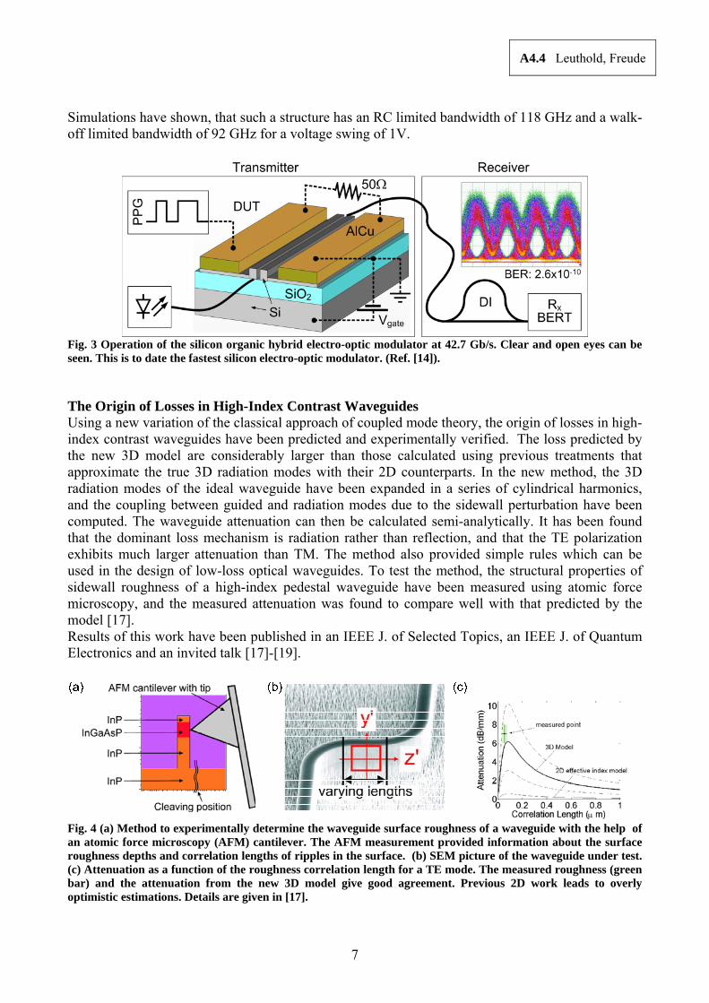
Simulations have shown, that such a structure has an RC limited bandwidth of 118 GHz and a walk-off limited bandwidth of 92 GHz for a voltage swing of 1V.
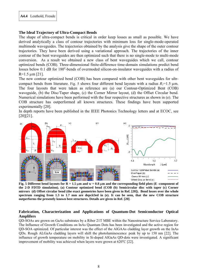
Fig. 3 Operation of the silicon organic hybrid electro-optic modulator at 42.7 Gb/s. Clear and open eyes can be seen. This is to date the fastest silicon electro-optic modulator. (Ref. [14]). The Origin of Losses in High-Index Contrast Waveguides Using a new variation of the classical approach of coupled mode theory, the origin of losses in high-index contrast waveguides have been predicted and experimentally verified. The loss predicted by the new 3D model are considerably larger than those calculated using previous treatments that approximate the true 3D radiation modes with their 2D counterparts. In the new method, the 3D radiation modes of the ideal waveguide have been expanded in a series of cylindrical harmonics, and the coupling between guided and radiation modes due to the sidewall perturbation have been computed. The waveguide attenuation can then be calculated semi-analytically. It has been found that the dominant loss mechanism is radiation rather than reflection, and that the TE polarization exhibits much larger attenuation than TM. The method also provided simple rules which can be used in the design of low-loss optical waveguides. To test the method, the structural properties of sidewall roughness of a high-index pedestal waveguide have been measured using atomic force microscopy, and the measured attenuation was found to compare well with that predicted by the model [17]. Results of this work have been published in an IEEE J. of Selected Topics, an IEEE J. of Quantum Electronics and an invited talk [17]-[19].
Fig. 4 (a) Method to experimentally determine the waveguide surface roughness of a waveguide with the help of an atomic force microscopy (AFM) cantilever. The AFM measurement provided information about the surface roughness depths and correlation lengths of ripples in the surface. (b) SEM picture of the waveguide under test. (c) Attenuation as a function of the roughness correlation length for a TE mode. The measured roughness (green bar) and the attenuation from the new 3D model give good agreement. Previous 2D work leads to overly optimistic estimations. Details are given in [17].
A4.4 Leuthold, Freude
8
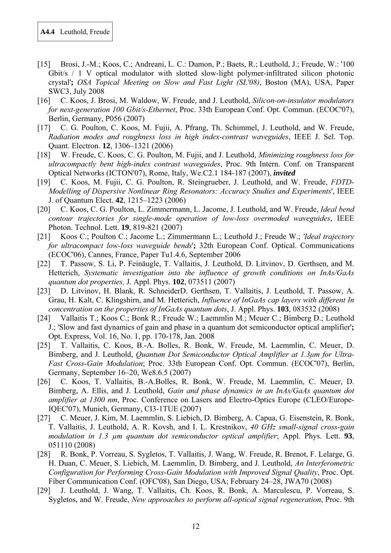
The Ideal Trajectory of Ultra-Compact Bends The shape of ultra-compact bends is critical in order keep losses as small as possible. We have derived analytically a class of contour trajectories with minimum loss for single-mode-operated multimode waveguides. The trajectories obtained by the analysis give the shape of the outer contour trajectories. They have been derived using a variational approach. The trajectories of the inner contour of the bent waveguides are then optimized such that there is no single-mode to multi-mode conversion. As a result we obtained a new class of bent waveguides which we call, contour optimized bends (COB). Three-dimensional finite-difference time-domain simulations predict bend losses below 0.1 dB for 180o-bends of overmoded silicon-on-insulator waveguides with a radius of R=1.5 m [21]. The new contour optimized bend (COB) has been compared with other bent waveguides for ultr-compact bends from literature. Fig. 5 shows four different bend layouts with a radius R1=1.5 m. The four layouts that were taken as reference are (a) our Contour-Optimized Bent (COB) waveguide, (b) the Disc/Taper shape, (c) the Corner Mirror layout, (d) the Offset Circular bend. Numerical simulations have been performed with the four respective structures as shown in (e). The COB structure has outperformed all known structures. These findings have been supported experimentally [20]. In depth reports have been published in the IEEE Photonics Technology letters and at ECOC, see [20][21].
|So
1,i1
| [dB
]
Fig. 5 Different bend layouts for R = 1.5 m and w = 0.8 m and the corresponding field plots (E -component of the 2-D FDTD simulation). (a) Contour optimized bend (COB (b) Semicircular disc with taper (c) Corner mirrors (d) Offset circular bend (the exact geometries have been given in Ref. [20]). Bend losses over the whole spectrum ranging from 1.3 to 1.7 mm are depcit3ed in (e). It can be seen, that the new COB structure outperforms the presently known best structures. Details are given in Ref. [20]. Fabrication, Characterization and Applications of Quantum-Dot Semiconductor Optical Amplifers QD-SOAs are grown on GaAs substrates by a Riber 21T MBE within the Nanostructure Service Laboratory. The Influence of Growth Conditions on InAs Quantum Dots has been investigated and the active region for QD-SOA optimized. Of particular interest was the effect of the AlGAAs cladding layer growth on the InAs QDs. Rough ALGaAs cladding layers will shift the photoluminescence peak by up to 150 nm [22]. The influence of growth temperature on mobility in Si-doped AlGaAs QD-dots were investigated. A significant improvement of mobility was achieved when layers were grown at 620oC [22].
A4.4 Leuthold, Freude
9
1 - 2 · 10 18 cm-3
1.4 · 10 18 cm-3
5 · 10 17 cm-3
1.7 · 10 18 cm-3
3 · 10 17 cm-3
n- GaAs: Si
n- GaAs:SiSubstrate
n- Al0.30 Ga0.70 As:Si
p - Al0.30 Ga0.70 As:Be
GaAs
GaAsactive layer
p- GaAs:Be
145 nm
1540 nm
100 nm
145 nm
1590 nm
700 nm
350 m
243 nm
1 - 2 · 10 18 cm-3
1.4 · 10 18 cm-3
5 · 10 17 cm-3
1.7 · 10 18 cm-3
3 · 10 17 cm-3
n- GaAs: Si
n- GaAs:SiSubstrate
n- Al0.30 Ga0.70 As:Si
p - Al0.30 Ga0.70 As:Be
GaAs
GaAsactive layer
p- GaAs:Be
145 nm
1540 nm
100 nm
145 nm
1590 nm
700 nm
350 m
243 nm
n- GaAs: Si
n- GaAs:SiSubstrate
n- Al0.30 Ga0.70 As:Si
p - Al0.30 Ga0.70 As:Be
GaAs
GaAsactive layer
p- GaAs:Be
145 nm
1540 nm
100 nm
145 nm
1590 nm
700 nm
350 m
243 nm
50 nm GaAs
6nm In0.18Ga0.82As
2.7ML InAs QDs
2nm In0.18Ga0.82 As
50nm GaAs Spacer
Active Region:
5x QD Layer:
50 nm GaAs
6nm In0.18Ga0.82As
2.7ML InAs QDs
2nm In0.18Ga0.82 As
50nm GaAs Spacer
Active Region:
5x QD Layer:
50 nm GaAs
6nm In0.18Ga0.82As
2.7ML InAs QDs
2nm In0.18Ga0.82 As
50nm GaAs Spacer
Active Region:
5x QD Layer:
Fig. 6 (a) Influence of surface roughness within AlGaAs cladding layer onto photoluminescence peak, see Ref. [23], (b) Structure of Quantum-Dot Semiconductor Optical Amplifer. To investigate the ultrafast nonlinear amplitude and phase dynamics behavior of QD-SOAs, we built a heterodyne pump-probe setup [24]. Features of which are, Operation at 1.3µm and 1.55µm , the temporal resolution <1 ps, Pump and probe co-polarized. The setup of the pump-probe pulse with phase-characterization capabilities is depicted in Fig. 7.
Fig. 7 Schematic of the heterodyne pump-probe setup. Short pulses are generated by an optical parametric oscillator (OPO) and split into pump, probe and reference pulses in a polarizing beam splitter (PBS). Probe and reference pulses are tagged by a frequency shift fprb and fref, respectively, which is induced by acousto-optic modulators (AOM). A strong pump pulse drives the SOA into its nonlinear regime and can be attenuated by the combination of the half-wave plate and the second polarizing beam splitter. A weak pulse probes these nonlinearities in gain and phase. After the device under test (DUT), the pulse train is split and recombined in a Michelson interferometer with unbalanced arm lengths such that the resulting probe-reference beat signal with frequency fref-fprb can be detected in amplitude and phase by a lock-in amplifier. (Ref. [24]) The experimental data of a pump-probe measurement of a typical QD SOA for a bias current of 100 mA which corresponds to a current density of i = 1.25 kA/cm2 and a pump power of -11 dBm (dots) are shown in Fig. 8. The Pump-probe measurements of QD SOA reveal two characteristic timescales [25]-[27], firstly a small time constant attributed to quantum dot carrier capture times. This fast process that dominates the quantum dot dynamics during the first 10 picoseconds determines mainly the material gain response and shows a very small alpha-factor, i.e. a small chirp. Secondly a large time constant associated with the slow refilling of the wetting layers governs the quantum-dot dynamics in the time frame after 15 ps. It contributes only little to the gain dynamics but since the associated alpha-factor is large (between 1 and 22 depending on the operating conditions) it dominates the phase response of the device and may significantly contribute to chirp.
A4.4 Leuthold, Freude
10
Fig. 8 Time evolution of (a) gain suppression G/G0 and (b) phase dynamics of a typical QD SOA device for a bias current density of i = 1.25 kA/cm2. The fit (solid line) well reproduces the measured data (gray dots). The model assumes a fast process (dashed line), a slow process (long-dashed line) and instantaneous two-photon absorption (TPA, dash-dotted line). (Ref. [25]) Based on the phase- and amplitude characteristics depicted in Fig. 8 we have introduced a filter scheme to perform all-optical wavelength conversion. Fig. 8 actually shows, that unlike with bulk semiconductor optical amplifers (SOAs) there is too little phase dynamics to perform all-optical operation. Additionally, one can see, that the phase dynamics is slow. Thus a filter scheme for cross-gain modulation rather than cross-phase modulation was needed. We have introduced a delay-interferomter (DI) filter after the QD-SOA. The DI was operated such that it would act on the amplitude rather than on the phase. An in-detailed description has been given in Ref. [28]. Fig. 9 shows the eye of a cross-gain experiment performed without and with filter. The filter obviously tremendously improved the eye opening. More results of the quantum-dot activities have been presented elsewhere [29]-[32].
Fig. 9 Eye diagrams of QD-SOA at operating point. (a) Eye diagram of the converted signal after SOA and (b) after DI. (Ref. [1]-[2])
A4.4 Leuthold, Freude
11
References
[1] Alloatti L., Korn D., Hillerkuss D., Vallaitis T., Li J., Bonk R., Palmer R., Schellinger T., Barklund A., Dinu R., Wieland J.,Fournier M., Fedeli J., Bogaerts W., Dumon P., Baets R., Koos C., Freude W., LeutholdJ.; 'Silicon High-Speed Electro-Optic Modulator', Group IV Photonics 2010, China, paper ThC2 Sept. 2010
[2] Alloatti L., Korn D., Hillerkuss D., Vallaitis T., Li J., Bonk R., Palmer R., Schellinger T., Barklund A., Dinu R., Wieland J., Fournier M., Fedeli J., Dumon P., Baets R., Koos C., Freude W., Leuthold J.; '40 Gbit/s Silicon-Organic Hybrid (SOH) Phase Modulator', ECOC 2010, Torino, Italy, Paper Tu.5.C.4, September 2010
[3] C. Koos, P. Vorreau, T. Vallaitis, P. Dumon, W. Bogaerts, R. Baets, B. Esembeson, I. Biaggio, T. Michinobu, F. Diederich, W. Freude, and J. Leuthold, All-Optical Signal Processing With Silicon-Organic Hybrid Slot Waveguides, Nature Photonics, April 2009
[4] Brosi J.-M.; Leuthold J.; Freude W.;'Microwave-frequency experiments validate optical simulation tools and demonstrate novel dispersiontailored photonic crystal waveguides'; J. Lightw. Technol., Vol. 25, No. 9, pp. 2502-2510, Sept. 2007
[5] Freude W.;Brosi J.-M. ; Koos C. ; Vorreau P.; Andreani, L. C.; Dumon P.; Baets R.; Esembeson B.; Biaggio I.; Michinobu T.; Diederich F.; and Leuthold J. ; “Silicon-Organic Hybrid (SOH) Devices for Nonlinear Optical Signal Processing”; Proc. 10th International Conference on Transparent Optical Networks (ICTON‘2008); Athens, Greece, paper Tu.C2.1, June 2008, invited
[6] J. Leuthold1, W. Freude, J.-M. Brosi, R. Baets, P. Dumon, I. Biaggio, M.L. Scimeca, F. Diederich, B. Frank, C. Koos; “Silicon Organic Hybrid Technology A Platform for Practical Nonlinear Optics”, to be published in the Proceedings of the IEEE; (invited)
[7] C. Koos, P. Vorreau, P. Dumon, R. Baets, B. Esembeson, I. Biaggio, T. Michinobu, F. Diederich, W. Freude, and J. Leuthold, Highly-Nonlinear Silicon Photonics Slot Waveguide, Proc. Conference on Optical Fiber Communication 2008 (OFC'2008), PDP25, (2008)
[8] C. Koos, L. Jacome, C. Poulton, J. Leuthold, and Freude, Nonlinear silicon-on-insulator waveguides for all-optical signal processing, Opt. Express 15, 5976-5990 (2007)
[9] C. Koos, L. Jacome, C. Poulton, J. Leuthold, W. Freude, Nonlinear High Index-Contrast Waveguides with Optimum Geometry, Proc. Nonlinear Photonics Topical Meeting and Tabletop Exhibit 2007, Quebec, Canada, JWA2 (2007)
[10] Koos C., Brosi J., Vorreau P., Vallaitis T., Dumon P., Baets R., Esembeson B., Biaggio I., Michinobu T., Diederich F., Freude W.and Leuthold J.; 'Silicon-Organic Hybrid (SOH) Devices for Optical Signal Processing'; in Proc. Frontiers in Optics 2008, Optical Society of America (OSA) Annual Meeting 2008, Rochester, USA, paper FMG6, Oct. 2008, (invited)
[11] Freude, W.; Koos, C.; Brosi, J.-M.; Vorreau, P.; Dumon, P.; Baets, R.; Esembeson, B.; Biaggio, I.; Michinobu, T.; Diederich, F.; Leuthold, J.; 'Silicon photonics: The impact of silicon-organic hybrid systems'; 9th Intern. Conf. on Fiber Optics & Photonics (Photonics'08), New Delhi, India, Dec. 2009; (invited)
[12] T. Vallaitis, C. Heine, R. Bonk, C. Koos, B. Esembeson, I. Biaggio, T. Michinobu, F. Diederich, P. Dumon, R. Baets, W. Freude, and J. Leuthold, All-Optical Wavelength Conversion at 42.7 Gbit/s in a 4 mm Long Silicon-Organic Hybrid Waveguide, Conference on Optical Fiber Communication 2009 (OFC'2009), submitted
[13] T. Vallaitis, C. Koos, B. Esembeson, I. Biaggio, T. Michinobu, F. Diederich, P. Dumon, R. Baets, W. Freude, and J. Leuthold, Highly Nonlinear Silicon Photonics Slot Waveguides without Free Carrier Absorption Related Speed-Limitations, Proc. of 34rd European Conference on Optical Communication, (ECOC'08), Brüssel, Th.2.D.6 (2008)
[14] J.-M. Brosi, Ch. Koos, L. C. Andreani, M. Waldow, J. Leuthold, and Freude, High-speed low-voltage electro-optic modulator with a polymer-infiltrated silicon photonic crystal waveguide, Opt. Express 16, 4177-4191 (2008)
A4.4 Leuthold, Freude
12
[15] Brosi, J.-M.; Koos, C.; Andreani, L. C.: Dumon, P.; Baets, R.; Leuthold, J.; Freude, W.: '100 Gbit/s / 1 V optical modulator with slotted slow-light polymer-infiltrated silicon photonic crystal'; OSA Topical Meeting on Slow and Fast Light (SL'08), Boston (MA), USA, Paper SWC3, July 2008
[16] C. Koos, J. Brosi, M. Waldow, W. Freude, and J. Leuthold, Silicon-on-insulator modulators for next-generation 100 Gbit/s-Ethernet, Proc. 33th European Conf. Opt. Commun. (ECOC'07), Berlin, Germany, P056 (2007)
[17] C. G. Poulton, C. Koos, M. Fujii, A. Pfrang, Th. Schimmel, J. Leuthold, and W. Freude, Radiation modes and roughness loss in high index-contrast waveguides, IEEE J. Sel. Top. Quant. Electron. 12, 1306–1321 (2006)
[18] W. Freude, C. Koos, C. G. Poulton, M. Fujii, and J. Leuthold, Minimizing roughness loss for ultracompactly bent high-index contrast waveguides, Proc. 9th Intern. Conf. on Transparent Optical Networks (ICTON'07), Rome, Italy, We.C2.1 184-187 (2007), invited
[19] C. Koos, M. Fujii, C. G. Poulton, R. Steingrueber, J. Leuthold, and W. Freude, FDTD-Modelling of Dispersive Nonlinear Ring Resonators: Accuracy Studies and Experiments', IEEE J. of Quantum Elect. 42, 1215–1223 (2006)
[20] C. Koos, C. G. Poulton, L. Zimmermann, L. Jacome, J. Leuthold, and W. Freude, Ideal bend contour trajectories for single-mode operation of low-loss overmoded waveguides, IEEE Photon. Technol. Lett. 19, 819-821 (2007)
[21] Koos C.; Poulton C.; Jacome L.; Zimmermann L.; Leuthold J.; Freude W.; 'Ideal trajectory for ultracompact low-loss waveguide bends'; 32th European Conf. Optical. Communications (ECOC'06), Cannes, France, Paper Tu1.4.6, September 2006
[22] T. Passow, S. Li, P. Feinäugle, T. Vallaitis, J. Leuthold, D. Litvinov, D. Gerthsen, and M. Hetterich, Systematic investigation into the influence of growth conditions on InAs/GaAs quantum dot properties, J. Appl. Phys. 102, 073511 (2007)
[23] D. Litvinov, H. Blank, R. SchneiderD. Gerthsen, T. Vallaitis, J. Leuthold, T. Passow, A. Grau, H. Kalt, C. Klingshirn, and M. Hetterich, Influence of InGaAs cap layers with different In concentration on the properties of InGaAs quantum dots, J. Appl. Phys. 103, 083532 (2008)
[24] Vallaitis T.; Koos C.; Bonk R.; Freude W.; Laemmlin M.; Meuer C.; Bimberg D.; Leuthold J.; 'Slow and fast dynamics of gain and phase in a quantum dot semiconductor optical amplifier'; Opt. Express, Vol. 16, No. 1, pp. 170-178, Jan. 2008
[25] T. Vallaitis, C. Koos, B.-A. Bolles, R. Bonk, W. Freude, M. Laemmlin, C. Meuer, D. Bimberg, and J. Leuthold, Quantum Dot Semiconductor Optical Amplifier at 1.3μm for Ultra-Fast Cross-Gain Modulation; Proc. 33th European Conf. Opt. Commun. (ECOC'07), Berlin, Germany, September 16–20, We8.6.5 (2007)
[26] C. Koos, T. Vallaitis, B.-A.Bolles, R. Bonk, W. Freude, M. Laemmlin, C. Meuer, D. Bimberg, A. Ellis, and J. Leuthold, Gain and phase dynamics in an InAs/GaAs quantum dot amplifier at 1300 nm, Proc. Conference on Lasers and Electro-Optics Europe (CLEO/Europe-IQEC'07), Munich, Germany, CI3-1TUE (2007)
[27] C. Meuer, J. Kim, M. Laemmlin, S. Liebich, D. Bimberg, A. Capua, G. Eisenstein, R. Bonk, T. Vallaitis, J. Leuthold, A. R. Kovsh, and I. L. Krestnikov, 40 GHz small-signal cross-gain modulation in 1.3 µm quantum dot semiconductor optical amplifier; Appl. Phys. Lett. 93, 051110 (2008)
[28] R. Bonk, P. Vorreau, S. Sygletos, T. Vallaitis, J. Wang, W. Freude, R. Brenot, F. Lelarge, G. H. Duan, C. Meuer, S. Liebich, M. Laemmlin, D. Bimberg, and J. Leuthold, An Interferometric Configuration for Performing Cross-Gain Modulation with Improved Signal Quality, Proc. Opt. Fiber Communication Conf. (OFC'08), San Diego, USA; February 24–28, JWA70 (2008)
[29] J. Leuthold, J. Wang, T. Vallaitis, Ch. Koos, R. Bonk, A. Marculescu, P. Vorreau, S. Sygletos, and W. Freude, New approaches to perform all-optical signal regeneration, Proc. 9th
[30] Bonk, R.; Sygletos, S.; Vorreau, P.; Vallaitis, T.; Wang, J.; Freude, W.; Leuthold, J.; Brenot, R.; Lelarge, F.; Duan, G.H.; 'Performance analysis of an interferometric scheme for media with limited cross-phase modulation nonlinearity'; Proc. 6th Intern. Symp. on Communication Systems, Networks and Digital Signal Processing ( CNSDSP'08), Graz, Austria, pp. 487– 491, July 2008 (best paper award)
[31] R. Bonk, C. Meuer, T. Vallaitis, S. Sygletos, P. Vorreau, S. Ben-Ezra, S. Tsadka, A. R. Kovsh, I. L. Krestnikov, M. Laemmlin, D. Bimberg, W. Freude, and J. Leuthold, Single and Multiple Channel Operation Dynamics of Linear Quantum-Dot Semiconductor Optical Amplifier, Proc. European Conference on Optical Communications (ECOC), Brussels, Belgium, Th.1.C.2 (2008)
[32] R. Bonk, R. Brenot, C. Meuer, T. Vallaitis, A. Tussupov, J. C. Rode, S. Sygletos, P. Vorreau, F. Lelarge, G. H. Duan, H.-G. Krimmel, Th. Pfeiffer, D. Bimberg, W. Freude, and J. Leuthold, 1.3/1.5 μm QD-SOAs for WDM/TDM GPON with Extended Reach and Large Upstream / Downstream Dynamic Range, Conference on Optical Fiber Communication 2009 (OFC'2009), submitted (2008)