29
UNCLASSIFIED AD 295 746 4 as ARMED SERVICES TECHNICAL INFORMATION AGENCY ARLINGTON HALL STATION ARLINGTON 12, VIRGINIA UNCLASSIFIED
UNCLASSIFIED
AD 295 746
4 as
ARMED SERVICES TECHNICAL INFORMATION AGENCYARLINGTON HALL STATIONARLINGTON 12, VIRGINIA
UNCLASSIFIED
NOTICE: When government or other drawings, speci-fications or other data are used for any purposeother than in connection with a definitely relatedgovernment procurement operation, the U. S.Government thereby incurs no responsibility, nor anyobligation whatsoever; and the fact that the Govern-ment may have formulated, furnished, or in any waysupplied the said drawings, specifications, or otherdata is not to be regarded by implication or other-wise as in any manner licensing the holder or anyother person or corporation, or conveying any rightsor permission to manufacture, use or sell anypatented invention that may in any way be relatedthereto.

hp associates. 2900 park boulevard palo alto, califomia D A i.8io
_- 1, 6-957
I - INVESTIGATION OF HOT ELECTRON EMITTER
C;
C0 -hp associates-(=) 2900 Park Boulevard
Palo Alto, California
Contract No. AF19(628)-1637_Project No. 4608Task 460804
SCIENTIFIC REPORT NO. 2
* September 1, 1962 - November 30, 1962Cwq A ST A
FEB 8 19Prepared
forELECTRONIC RESEARCH DIRECTORATEAIR FORCE CAMBRIDGE RESEARCH LABORATORIES
OFFICE OF AEROSPACE RESEARCHUNITED STATES AIR FORCEBEDFORD, MASSACHUSETTS
an affiliate of He wle tt-Packa rd Company
Requests for additional copies by Agencies of
the Department of Defense, their contractors, and
other Government Agencies should be directed to the:
ARMED SERVICES TECHNICAL INFORMATION AGENCYARLINGTON HALL STATIONARLINGTON 129 VIRGINIA
Department of Defense contractors must be es-
tablished for ASTIA services or have their "need to
know" certified by the cognizant military agency of
their Droject or contract.
All other persons and organizations should apply
to the:
U. S. DEPARTMENT OF COMMERCEOFFICE OF TECHNICAL SERVICES
WASHINGTON 25, D. C.
TABLE OF CONTENTS
Section Page No.
ABSTRACT i
I INTRODUCTION 1
II COMPARISON OF TRIODES
II.1 Mechanisms of Operation 1
11.2 Basic Emitter Characteristics 3
11.3 Emitter Conductance 5
11.4 Emitter Figure-of-Merit gm/Ce 6
11.5 Triode Amplifier Gain-Band ProductFivure-of-Merit 7
III PERSONNEL 11
IV VISITORS, CONFERENCES AND TRAVEL 11
ABSTRACT
Analysis is presented of the frequency performance
of various metal-base hot carrier triode amplifiers which
differ only in the type of hot carrier emitter they utilize.
The triodes considered are: (1) The SMS, or semiconductor-
metal-semiconductor triode utilizing a Schottky barrier
emitter; (2) The space charge limited emitter triode; and
(3) The tunnel-emitter triode. The results are compared
with the performance of the bipolar permanium junction trans-
istor. It is shown that for all three hot carrier triodes,
the maximum gain-band product increases with current density
and approaches an assvmptotic limit of about 1.4x10⁸/S which
is due to collector limitation, where S is the stripe width
in cm. It is further shown, however, that this limit is
closely approached at reasonable current density only by the
SMS triode. This limit is to be compared with a value of
(5 to 12)106/S for the germanium transistor.
At an emitter current density of 1000 amp/cm 2 and
a stripe width of 10 microns, the maximum gain-band products,
or maximum oscillatinp frequencies, are 60 kmc/sec for the
SMS triode, 38 for the space charge limited emitter triode,
and 10 for the tunnel-emitter triode.
i
I INTRODUCTION
Considerable interest has been recently generated
in solid state triode amplifiers based on hot carrier trans-
port in thin metal films. Various structures have been pro-
posed1 " and evidence of hot carrier triode action has been
demonstrated.3' 5' 6 Furthermore, independent measurements of
transport of hot carriers in various metal films have been
carried out7' indicating ranges as high as several hundred
Anestroms in the one electron volt energy range.
Three main hot carrier triode structures have been
proposed, These are listed in Table I, together with other
more conventional triode amplifiers. The basic operation of
the three hot carrier triodes indicated is essentially the
same. They differ, however, in one all-important respect,
namely, the structure of the emitter and the mechanism of
hot carrier injection into the metal base. The consequences
of utilizing the various emitters indicated, on the overall
amplifier characteristics, and particularly its high fre-
quency limitations, are developed and presented in this re-
port. Comparisons are also made with the performance of the
more conventional bipolar transistor.
II COMPARISON Or TRIODES
I1.1 Mechanisms of Operation
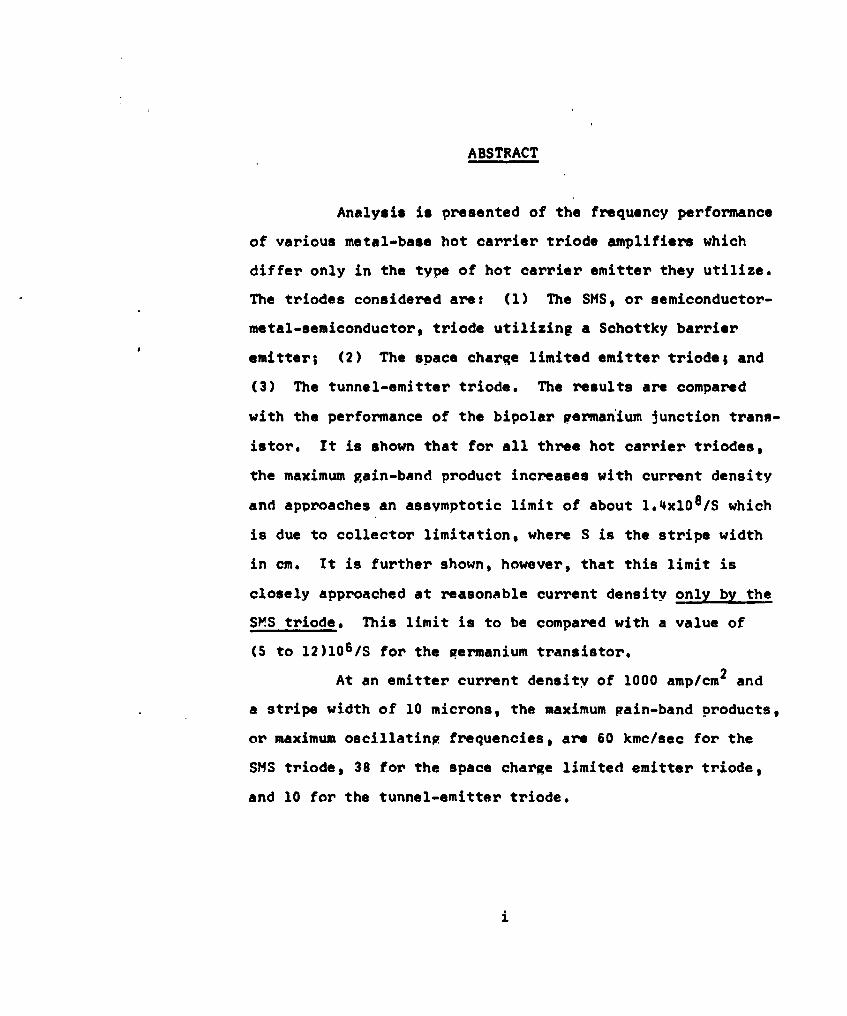
Figure 1 is a schematic presentation of the enerov band
diagram for each of the triodes cornared. Diaeram 1 represents
a conventional npn transistor. Diapram 2 represents a tunnel
emitter hot electron triode. Hot electrons are iniected into
- 1-
TABLE I
SOME PPOPOSED OF EXISTING TRIODE AMPLIFIERS
I BiDolar Transistors (1) non or DnD
II UniDolar Transistors (2) Field effect transistor
(a) junction transistors
(b) surface transistors
(3) Analoque transistor
ITT Hot Cerr~er Triodes (4) Tunnel emitter triode
(5) SDace charge limitedemitter triode
(6) (SMS) Schottkv emittertriode
-I.

the metal base by quantum mechanical tunneling through a
thin insulating layer "W". Hot electrons transported across
the metal base without collision are collected by passing
over a lower energy base-collector barrier into the space
charge of the reverse biased collector. Diagram 3 represents
a hot electron triode with space charge limited emitter. Hot
electrons are injected into the metal base by flowing from a
metal (extreme left) into the conduction band of an insulating
film "W" (or hiph resistivity semiconductor) and finally into
the metal bases The electron flow in the emitter region "W"
in this case is determined by the space charge of the flowing
electrons. Diagram 3 represents the SMS or semiconductor-
metal-semiconductor hot electron triode. The emitter is es-
sentially a Schottky-type barrier which is so chosen that in
forward bias, current flow is primarily due to majority car-
riers in the semiconductor (in this case electrons). This
current will flow into the metal base as hot electrons.
11.2 Basic Emitter Characteristics
The emitter characteristics pertinent to our discus-
sion are the capacitance-voltage and current density-voltage
characteristics under forward bias. These are summarized in
Table II.
The assumptions and notations used are as follows:
(1) For the npn transistor emitter, the emitter junction is a
step np junction of unity injection efficiency. The base region
-3-

TABLE II
COMPARISON OF BASIC EMITTER CHARACTERISTICS
Capacitance (C) - Current Density (je) -Triode Voltage (U) Voltage (U)
qN nj.2 D U(1) npn Transistor C. It q R- b j ( -1)
(2) Tunnel Emitter C .) U xTriod C z . e x 0'(1)( 2
6.82x10⁷ 3/2
exp t u/we )
(3) Space ChargeLimited Emitter 3Triode Ce 1 i - iu2/WO3
C TV e e 32w
F qN* 1 -q Vq U
(4) SMS Triode C* T q! e 1/2b eJ: qvoNee
*All equations are in esu except where noted.
ICUnits are amp, volt, cm.
-I.-
Wb wide and is a concentration Nb. A unity base transport
factor is assumed, q is the electron charge, Vb is the bar-
rier height, U is the applied forward bias, K is the semicon-
ductor dielectric constant, ni is its intrinsic carrier den-
sity and Dn is the diffusion coefficient of electrons in the
base region. (2) For the tunnel-emitter triode, it is as-
sumed that current flow obeys a Fowler-Nordhiem relation of
field emission or tunneling through a triangular potential
barrier.8 Wa is the thickness of the insulating emitter film
through which tunneling occurs, # is the metal-insulator bar-
rier height, and K is the insulator's dielectric constanti
The numerical constants given correspond to T z 3000K. (3)
For the space charge limited emitter, it is assumed that the
emitter region We is free of fixed charges or traps and only
a single carrier is present. It is also assumed that through-
cut the region the carrier velocity equals PE where p and E
are the carrier mobility and electric field, respectively.
(4) For the SMS triode, the emitter barrier efficiency is
unity (i.e., no minority carriers are injected into the semi-
conductor), the emitter is uniformly doped to a concentration
Ne, the barrier height is Vb and vo is the electron thermal
velocity (kT/2wm)1 /2 in the semiconductor.
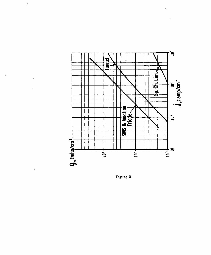
11.3 Emitter Conductance
Based on the relations given in Table II, the emitter
conductance p (die/dUe) was calculated for each triode at
different current densities. The results are shown in Figure 2
--
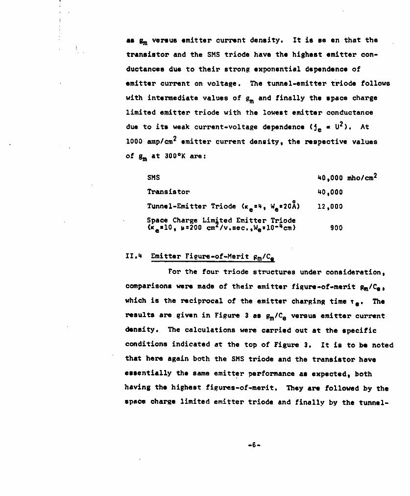
as gm versus emitter current density. It is so en that the
transistor and the SMS triode have the highest emitter con-
ductances due to their strong exponential dependence of
emitter current on voltage. The tunnel-emitter triode follows
with intermediate values of gm and finally the space charge
limited emitter triode with the lowest emitter conductance
due to its weak current-voltage dependence (Je a U2). At
1000 amp/cm2 emitter current density, the respective values
of gm at 300 0 K are:
SMS 40,000 mho/cm2
Transistor 40,0000
Tunnel-Emitter Triode ('e= 4 9 Wec20A) 12,000
Space Charge Lim ted Emitter Triode(KezlO Pz200 cm'/v.sec.$We=10 4 cm) 900
11.4 Emitter Figure-of-Merit gm/Ce
For the four triode structures under consideration,
comparisons were made of their emitter figure-of-merit gm/Ce,
which is the reciprocal of the emitter charging time Te . The
results are given in Figure 3 as gn/Ce versus emitter current
density. The calculations were carried out at the specific
conditions indicated at the top of Figure 3. It is to be noted
that here again both the SMS triode and the transistor have
essentially the same emitter performance as expected, both
having the highest figures-of-merit. They are followed by the
space charge limited emitter triode and finally by the tunnel-
-6-
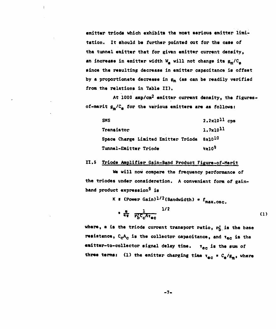
emitter triode which exhibits the most serious emitter limi-
tation. It should be further pointed out for the case of
the tunnel emitter that for given emitter current density,
an increase in emitter width We will not change its gm/Ce
since the resulting decrease in emitter capacitance is offset
by a proportionate decrease in gm (as can be readily verified
from the relations in Table II).
At 1000 amp/cm 2 emitter current density, the figures-
of-merit sm/Ce for the various emitters are as follows:
SMS 2.2x101 l cps
Transistor l.7x10 1 1
Space Charge Limited Emitter Triode 6x101 0
Tunnel-Emitter Triode 4xl09
11.5 Triode Amplifier Gain-Band Product Figure-of-Merit
We will now compare the frequency performance of
the triodes under consideration. A convenient form of gain-
band product expression9 is
K I (Power Gain)1 /2 (Bandwidth) a fmaxosc,
a 1 1/2
where, a is the triode current transport ratio, q in the base
resistance, CcAc is the collector capacitance, and Tec is the
emitter-to-collector signal delay time. Tec is the sum of
three terms: (1) the emitter charging time vec a Ce/gm, where
-7-
gm and C. are the emitter conductance and capacitance per
unit area, respectively; (2) the base transit time Tb x
vthm where Wb is the metal base width, and Vth.m. is the
velocity of hot electrons in the metal; and (3) the collector
transit time Tc z 2v...., where Xm is the width of the2vsc.ljm.
collector depletion region, and Vsc~lim ,is the scatter
limiting drfit velocity of the carrier in the collector.
For all three hot electron triodes considered, the
base transit time is small and can be generally neglected
(for Wb a 10" 6cm, and Vth.m" a 108cm/sec., Tb g 10-14 sec.).
Hence
Tea - [Ce/gm + ] (2)
vsc.lim.
The dependence of Rain-band product K on base width Wb is,
therefore, only through the dependence of a and r' onb onWb.
Following Early's treatment of the bipolar junction
triodeg 0 consider a simple linear stripe geometry of unit
length with an emitter stripe width s, spaced s/2 from the
base stripes. The collector capacitance is then sCc, and the
base resistance r -Y SOmlWb where Cc is the collector capaci-
tance per unit area C: -AL . -LI, and om is the resistivity of
the metal base.
For a hot electron triode with unity emitter efficien-
cy, its gain is given by:
- Wbl/L
* (l-R)e (3)
-8-

where L is the hot electron range in the metal base, and
R is its reflection coefficient at the collector. Substi-
tuting for r;, CcAc, and a in Equation (1), gives:
K: l-R) 1,2 * Wb/2'IMF 2omcec .eb
K, obviously, has a maximum which is reached when Wb = L/29
i.e., when the base width is just one half the hot electron
range:
K mxC1RL)1/2 (5max OmCcTec
Substituting for Tec from Equation (2) gives:
K 1-R 1/2
Kma x 5 61 + 2 j
vsc.lim . 7m
This relation is aDplicable to all three hot electron triodes
under consideration. It indicates the dependence of Kmax on
the figure-of-merit (9m/Ce) of the specific type of emitter
which the triode utilizes. From the dependence of (gm/Ce) on
emitter current density jet as discussed in Section 11.4 and
presented in Figure 3, and from Equation (6) one obtains the
dependence of Kmax on emitter current density. This calculation
was carried out and the results are given in Figure 4 as Kmax
versus emitter current density for the three hot electron triodes
-9-
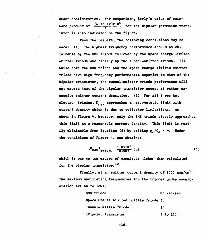
under consideration. For comparison, Early's value of gain-
band product of (s to s2)xlO for the bipolar germanium trans-
istor is also indicated on the figure.
From the results, the following Conclusions may be
made: (1) The highest frequency performance should be ob-
tainable by the SMS triode followed by the space charge limited
emitter triode and finally by the tunnel-emitter triode. (2)
While both the SMS triode and the space charge limited emitter
triode have high frequency performances superior to that of the
bipolar transistor, the tunnel-emitter triode performance will
not exceed that of the bipolar transistor except at rather ex-
cessive emitter current densities. (3) For all three hot
electron triodes, Kmax approaches an assymptotic limit with
current density which is due to collector limitations. As
shown in Figure 4, however, only the SMS triode closely approaches
this limit at a reasonable current density. This limit is read-
ily obtainable from Equation (6) by setting gm/Ce : *. Under
the conditions of Figure 4, one obtains:
(Kma ) 1.4xl0(
.maxassym. srcml cps
which is one to two orders of magnitude higher than calculated
for the bipolar transistor.10
Finally, at an emitter current density of 1000 amp/cm2 ,
the maximum oscillating frequencies for the triodes under consid-
eration are as follows:
SMS triode 60 kmc/sec.
Space Charge Limited Emitter Triode 38
Tunnel-Emitter Triode 10
(Bipolar transistor 5 to 12)
-10-
III PERSONNEL
Individuals who contributed to the contract activ-
ity in this report period are:
M. M. Atalla
R. W. Soshea
R. C. Lucas
C. H. Fox
D. A. Reid
V. M. Dowler
IV VISITORS, CONFERENCES AND TRAVEL
Visitors
There were no visitors to our Laboratory during this
report period.
Conferences
Dr. M. M. Atalla presented a paper entitled "The Hot
Electron Triode with Semiconductor Metal Emitter" at the 1962
NEREM Conference held November 5, 6 and 7 at Boston, Massachusetts.
Travel
Dr. M. M. Atalla visited the ArCRC Laboratories on
November 8, 1962 to discuss contract progress with Mr. R. F.
Cornelissen's group.
-11-
BIBLIOGRAPHY
1. C. A. Head;. Proc. IRE 48, 1359; (1960).
2. J. P.- Spratt, R. F. Schwarz, and W, M, Kane; Phys. Rev,Letters 6. 341; (1961).
3. M. H. Atalla and D. Kahng; IRE-AZEE Device-ResearchConference, University of New Hampshire; (July, 1962).
4. D. V. Geppert; Proc. IRE 50, 1527; (1962).
5o D. Kahng; Proc. IRE 50, 1534; (1962).
6. M. M. Atalla, NEREH Record, 162; (1962).
7. W. Go Spitzer, C. R. Crowell$ and H. H, Atalla;g Phys.Rev. Letters 8, 57; (1962).
8. A. Go Chynoweth; Progress in Semiconductors 4, 97; (1959).
9. R. L. Pritchard; "Frequency Response of Grounded Base andGrounded Emitter Transistors". given at AIEE Winter Meeting,Now York, N.Y.; January, 1954.
10. J. H. Early; Proc. IRE 469 1924-27; December, 1958.
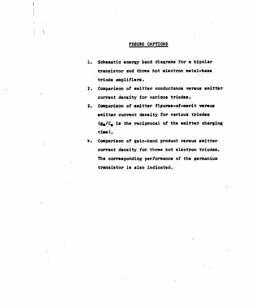
FIGURE CAPTIONS
1. Schematic energy band diagrams for a bipolar
transistor and three hot electron metal-base
triode amplifiers.
2. Comparison of emitter conductance versus emitter
current density for various triodes.
3. Comparison of emitter figures-of-merit versus
emitter current density for various triodes
(gm/Ce is the reciprocal of the emitter charging
time).
4. Comparison of gain-band product versus emitter
current density for three hot electron triodes.
The corresponding performance of the germanium
transistor is also indicated.
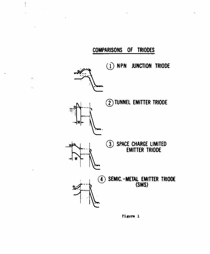
COMPARISONS OF TRIODES
, (f@ NPN JUNCTION TRIODE
TUNNEL EMITTER TRIODE
03) SPACE CHARGE LIMITEDEMITTER TRIODE
SEMIC. -METAL EMITTER TRIODEFI ur(SMS)
Figure 1
ifi
Figure

EMITTER FIGURE OF MERIT ( gm/C 6)
(DSemiconductor-metal : Si-Au, No _10 16/cm3
T NPN : Nb-101T/cm 3 , Wbil( 4 cm
(I) Space charge limited : W. -lO1 4cm
9m,. sec Tunnel emitter: c - Iev, w6-20ACe
1012.- I I 1 0 I
O,
4 O
10 10 10 10
e: amp/cm 2
Figure 3

COMPARISON OF GAIN-BANDWIDTH PRODUCTSLINEAR GEOMETRY
[(Power Gain)"'x Band Width] K 350A GOLD BASE- Si CollectorV0 8 10 Volts, VCB=5 Volts
- - - - - I Stripe Width 10 Microns
Semic-Metal +Collector Limiting-*10"_ -Ehitt r- -- - - -
1010 mittr - - - junction__Trode
Figure 4
DISTRIBUTION
Code Organization No. of Copies
AF 5 AFMTC(AFMTC Tech Library MU-135)Patrick Air Force BaseFlorida 1
AF 18 AULMaxwell Air Force BaseAlabama
AF 32 OAR (RROS, Col. John R. Fowler)Tempo D4th & Independence AvenueWashington 25, D.C. 1
AF 33 AFOSR, OAR (SRYP)Tempo D4th & Independence AvenueWashington 25, D.C.
AF 43 ASD (ASAPRD - Dist)Wright Patterson Air Force BaseOhio 1
AF 124 Rome Air Development Center(RAALD)Griffiss Air Force BaseNew YorkAttn: Documents Library
AF 139 AF Missile Development Center(MDGRT)Holloman Air Force BaseNew Mexico 1
AF 314 HeadquartersOAR (RROSP, Maj. Richard W. Nelson)Washington 25, D.C. 1
AF 318 ARL (ARA-2)Library AFL 2292, Building 450Wright-Patterson Air Force BaseOhio
Ar 5 Commanding GeneralUSASRDLFt. Monmouth, New JerseyAttn: Tech Doc. Ctr.
SIGRA/SL-ADT 1
Code Organization No. of Copies
AF 253 Technical Information OfficeEuropean Office, Aerospace ResearchShell Building47 CantersteenBrussels, Belgium 1
Ar 107 U.S. Army Aviation Human Research UnitU.S. Continental Army CommandP. O. Box 428Fort Rucker, AlabamaAttn: Maj. Arne H. Eliasson 1
G 8 LibraryBoulder LaboratoriesNational Bureau of StandardsBoulder, Colorado 2
M 63 Institute of the Aerospace SciencesInc.2 East 64th StreetNew York 21, New YorkAttn: Librarian 1
M 84 A.F. Cambridge Research LaboratoriesOAR (CRXR, J.R. Marple)L.G. Hanscom FieldBedford, Massachusetts 1
N 73 Office of Naval ResearchBranch Office, LondonNavy 100, Box 39F.P.O., New York, New York 6
U 32 Massachusetts Institute of TechnologyResearch LaboratoryBuilding 26, Room 327Cambridge 39, MassachusettsAttn: John H. Hewitt 1
U 431 Alderman LibraryUniversity of VirginiaCharlottesville, Virginia 1
G 9 Defence Research MemberCanadian Joint Staff2450 Massachusetts Avenue, N.W.Washington 8, D.C. 1
AF 137 Aeronautical Systems Division(ASRNEM, Mr. Richard Alberts)Wright-Patterson Air Force BaseOhio 1
Code Organization No. of Copies
Ar 9 Department of the AmyOffice of the Chief Signal OfficerWashington 25, D.C.Attn: SIGRD-4a-2 1
Ar 50 Commanding OfficerAttn: ORDTL-012Diamond Ordnance Fuze LaboratoriesWashington 25, D.C. 1
Ar 67 Redstone Scientific Information CenterU.S. Army Missile CommandRedstone Arsenal, Alabama 1
G 31 Office of Scientific IntelligenceCentral Intelligence Agency2430 E Street, N.W.Washington 25, D.C. 1
G 2 ASTIA (TIPAA)Arlington Hall StationArlington 12, Virginia 20
G 68 Scientific & Technical InformationFacility
Attn: NASA Representative (s-AK/DL)P. 0. Box 5700Bethesdag Maryland 1
G 109 DirectorLangley Research CenterNational Aeronautics & Space Administr.Langley Field, Virginia 1
N 9 Chief, Bureau of Naval WeaponsDepartment of the NavyWashington 25, D.C.Attn: DLI-31 2
N 29 Director (Code 2027)U.S. Naval Research LaboratoryWashington 25, D.C. 2
I 292 Director USAF Project RANDThe Rand Corporation1700 Main StreetSanta Monica, CaliforniaTHRU: AF Liaison Office 1
M 6 A.F. Cambridge Research LaboratoriesOAR (CRXRA - Stop 39)L.G. Hanscom FieldBedford, Massachusetts 20
Code Organization No. of Copies
Ar 83 U.S. Army Signal Research andDevelopment Laboratories
Attn: SIGRA/SL-PD, H. JacobsFort Monmouth, New Jersey 1
G 70 Advisory Group on Electron Devices(AGED)Office of the Director of Defense
Res. & Eng.346 Broadway$ 8th FloorNew York 13, New York 4
I 43 Radio Corporation of AmericaRCA LaboratoriesPrinceton, New JerseyAttn: Dr. P.K. Weimer
I 44 Bell Telephone Laboratories, Inc.Murray Hill, New JerseyAttn: Dr. J. Early
I 46 Coming Glass WorksCorningNew YorkAttn: Thomas C. MacAvoy
I 154 General Electric Research LaboratoriesP.O. Box 1088, The KnollsSchenectady, New YorkAttn: Dr. R. N. Hall
I 820 Raytheon CompanyResearch DivisionSeyon StreetWaltham, MassachusettsAttn: Jerome M. Lavine 1
I 979 Radio Corporation of AmericaRCA LaboratoriesPrinceton, New JerseyAttn: Dr. William Webster
M 60 ESD (ESRDE, Maj. James Van Horn)L.G. Hanscom FieldBedford, Massachusetts
N 79 Chief, Bureau of ShipsDepartment of the NavyTubes & Semiconductors Unit, Code 691A1Washington 25, D.C.Attn: Mr. A. H. Young
Code Organization No. of Copies
U 20 Niels I. MeyerPhysics DepartmentTechnical UniversitySolvgate 83Copenhagen, Denmark
HeadquartersA.F. Cambridge Research LaboratoriesOAR (CRRCSA-l. Dr. A. C. Yang)L.G. Hanscom FieldBedford, Massachusetts 9
IL~_ E
15 uE
~~~M H~
H iR
*IhU4.0. 0;.I 5,C
fJg II t
F E2
t- I - E
II


![menu art. or oo 00 FAX 075-746-5086 075-746-5087 https ...menu art. or oo 00 FAX 075-746-5086 075-746-5087 (QR2— F) ] 9 6 • •](https://static.documents.pub/doc/80x56/5ffe224c27cf63401d01a73f/menu-art-or-oo-00-fax-075-746-5086-075-746-5087-https-menu-art-or-oo-00-fax.jpg)