Dense wavelength-division-multiplexing (DWDM) technology is popularly used to increase
the transmission bandwidth of optical communication systems, where high-performance
multi/demultiplexers with wide channel passband, low crosstalk, and low polarization
dependence loss, are needed. Future optical communication systems require adaptive optical
devices, such as tunable lasers, variable optical attenuators, reconfigurable add/drop
multiplexers, and adaptive multi/demultiplexers. Furthermore, fiber optic technologies have
widely been applied to various areas such as fiber sensors, optical instrumentation and testing,
#127127 - $15.00 USD Received 16 Apr 2010; revised 18 May 2010; accepted 19 May 2010; published 25 May 2010(C) 2010 OSA 07 June 2010 / Vol. 18, No. 12 / OPTICS EXPRESS 12277
and microwave photonic systems, where adaptive multi/demultiplexers are crucial for the
effective processing of optical signals.
Different multi/demultiplexers designs have recently been reported, including the use of
[4]. However, these designs only enable the multi/demultiplexing of wavelength channels
with fixed wavelengths, bandwidth, and channel spacings, thus having limited
reconfigurability. Liquid crystal (LC) devices have long been developed for wavelength-
division multiplexing. A liquid crystal and grating based cross-connect 1×2 switch has been
reported, which can switch independently eight wavelength channels that are 4 nm apart [5].
More recently, a wavelength-selective switch (WSS) based on a Liquid Crystal on Silicon
(LCOS) switching element has been reported, which enables the demultiplexing WDM
channels into 9 fiber ports [6]. Microelectromechanical systems (MEMS) employing
micromirrors have also been explored for adding flexibility to signal demultiplexing and
routing in WDM systems [7, 8].
In this paper, we propose and experimentally demonstrate the principle of a novel
structure of an adaptive wavelength multi/demultiplexer based on the use of an Opto-VLSI
processor. Using computer-generated phase holograms uploaded onto an Opto-VLSI
processor, wavelength channels with variable and arbitrary channel spacings can be
multiplexed and steered into a common output fiber port. In addition, multiplexed wavelength
channels with variable and arbitrary channel spacings can be demultiplexed and steered into
any specific fiber ports. A proof-of-concept 1×3 adaptive WDM multi/demultiplexer structure
is developed, demonstrating multiplexing and demultiplexing of three WDM channels of
arbitrary wavelengths over the C-band.
2. Opto-VLSI processor
The Opto-VLSI processor is a diffraction element capable of steering/shaping an incident
optical beam electronically without mechanically moving parts [9]. An Opto-VLSI processor
comprises an array of liquid crystal (LC) cells driven by a Very-Large-Scale-Integrated
(VLSI) circuit, which generates digital holographic diffraction gratings (e.g. blazed gratings)
of arbitrary pitches, thus achieving arbitrary beam deflection/multicasting. A transparent
Indium-Tin Oxide (ITO) layer is used as the second electrode, and a quarter-wave-plate
(QWP) layer is deposited between the LC and the aluminum mirror to accomplish
polarization-insensitive operation. The voltage level of each pixel can individually be
controlled by using a few memory elements that select a discrete voltage level and apply it,
through the electrodes, across the LC cell. The diffraction angle, αm, for the Opto-VLSI
processor is given by:
arcsin( )m
m
d
λα = (1)
where m is the diffraction order (here only first order is considered), λ is the vacuum
wavelength, and d is the grating period.
#127127 - $15.00 USD Received 16 Apr 2010; revised 18 May 2010; accepted 19 May 2010; published 25 May 2010(C) 2010 OSA 07 June 2010 / Vol. 18, No. 12 / OPTICS EXPRESS 12278
3. Structure of the Opto-VLSI-based adaptive multi/demultiplexer
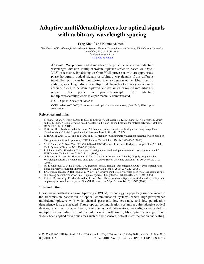
Fig. 1. The proposed adaptive multi/demultiplexer structure.
The proposed adaptive multi/demultiplexer is illustrated through an experimental setup in Fig.
1. The fiber collimator array provides the input and output ports. In the multiplexing mode,
arbitrary wavelength channels are input through Port 1, Port 2, and Port 3, and the
multiplexed signal is routed to Port C. The input wavelength channels are collimated, and
diffracted by a grating plate with 1200 line/mm along different directions, and mapped, by the
lens, onto the active window of the Opto-VLSI processor. According to Eq. (1) the
wavelength channels illuminating the different pixel blocks of the Opto-VLSI processor can
be either independently steered and coupled into Port C of the fiber collimator array with
minimum attenuation, or deliberately steered “off-track” so that they are partially coupled
into Port C, leading to arbitrary and independent optical attenuation for all wavelength
channels (as illustrated in the inset of Fig. 1). Note that, by reconfiguring the hologram
uploaded onto the Opto-VLSI processor, any of the wavelength channels can also be steered
and coupled into any port other than Port C. The demultiplexing mode is the reverse process
of multiplexing, but has a similar principle, where Port C serves as the input fiber port for an
input WDM multiplexed signal, while the demultiplexed channels are routed to the other
collimator ports.
When the wavelength of an input port changes, the corresponding collimated optical beam
is diffracted through the grating plate along a different direction, and mapped onto a different
pixel block, whereon an optimal phase hologram is uploaded to optimally steer the new
collimated optical beam and couple it into the desired output fiber port.
4. Experiments and results
In the experiments demonstrating the multiplexing mode, three tunable lasers (Agilent) were
used to supply three arbitrary input wavelength channels. The spacing between the fiber
collimator elements was 1 mm. A 256-phase-level two-dimensional Opto-VLSI processor
having 512×512 pixels was used for optical beam steering. A Labview software was
specifically developed to appropriately partition and drive the pixel blocks so that any
wavelength channel illuminating the active window of the Opto-VLSI processor can
#127127 - $15.00 USD Received 16 Apr 2010; revised 18 May 2010; accepted 19 May 2010; published 25 May 2010(C) 2010 OSA 07 June 2010 / Vol. 18, No. 12 / OPTICS EXPRESS 12279
independently be steered and coupled into Port C. By optimizing the size and the phase
profile of each pixel block, optimum optical beam steering was achieved corresponding to
maximum optical power coupling into the fiber ports, and hence minimum insertion loss for
each wavelength channel.
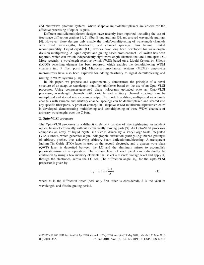
Fig. 2. Multiplexing operation of the proposed adaptive multi/demultiplexer
Figure 2 shows some experimental scenarios for the multiplexing operation of the
proposed adaptive multi/demultiplexer. In the scenario corresponding to Fig. 2(a), the
wavelength channels λ1=1550.12 nm, λ2=1556.06 nm, and λ3=1537 nm, were input through
Port 1 (we call Channel 1), Port 2 (Channel 2), and Port 3 (Channel 3), respectively. The three
channels, whose wavelength values were randomly set, were mapped onto the different pixel
blocks on the Opto-VLSI processor. By independently and simultaneously uploading
optimized phased holograms to the corresponding pixel blocks, each wavelength channel was
coupled into Port C. The multiplexed signal, shown in Fig. 2(a), was monitored by an optical
spectral analyzer. In the scenario corresponding to Fig. 2(b), the wavelength of Channel 2 was
changed to λ2=1541 nm and the others were not changed. Hence, the optical beam associated
to Channel 2 was mapped onto a different position on the pixellated surface of the Opto-VLSI
processor, while those corresponding to Channel 1 and Channel 3 were unchanged. In this
case, the phase hologram responsible for steering Channel 2 to Port C was shifted to the pixel
block where λ2 was mapped. The measured multiplexed signal at Port C is shown in Fig. 2
(b), which indicates that the three channels were successfully multiplexed. More complex
multiplexing operations were demonstrated in the scenarios corresponding to Fig. 2(c) and
Fig. 2(d), where two and three wavelength channels were changed, in comparison to the
WDM profile shown Fig. 2(b). By applying appropriate phase holograms to the
corresponding illuminated pixel blocks, the three wavelength channels were successfully
multiplexed, as illustrated in Fig. 2(c) and Fig. 2(d), respectively.
#127127 - $15.00 USD Received 16 Apr 2010; revised 18 May 2010; accepted 19 May 2010; published 25 May 2010(C) 2010 OSA 07 June 2010 / Vol. 18, No. 12 / OPTICS EXPRESS 12280
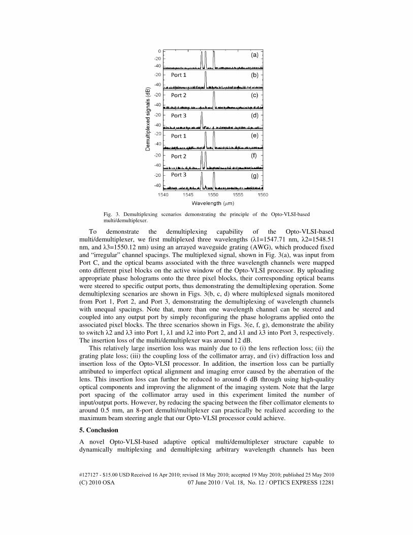
Fig. 3. Demultiplexing scenarios demonstrating the principle of the Opto-VLSI-based
multi/demultiplexer.
To demonstrate the demultiplexing capability of the Opto-VLSI-based
multi/demultiplexer, we first multiplexed three wavelengths (λ1=1547.71 nm, λ2=1548.51
nm, and λ3=1550.12 nm) using an arrayed waveguide grating (AWG), which produced fixed
and “irregular” channel spacings. The multiplexed signal, shown in Fig. 3(a), was input from
Port C, and the optical beams associated with the three wavelength channels were mapped
onto different pixel blocks on the active window of the Opto-VLSI processor. By uploading
appropriate phase holograms onto the three pixel blocks, their corresponding optical beams
were steered to specific output ports, thus demonstrating the demultiplexing operation. Some
demultiplexing scenarios are shown in Figs. 3(b, c, d) where multiplexed signals monitored
from Port 1, Port 2, and Port 3, demonstrating the demultiplexing of wavelength channels
with unequal spacings. Note that, more than one wavelength channel can be steered and
coupled into any output port by simply reconfiguring the phase holograms applied onto the
associated pixel blocks. The three scenarios shown in Figs. 3(e, f, g), demonstrate the ability
to switch λ2 and λ3 into Port 1, λ1 and λ2 into Port 2, and λ1 and λ3 into Port 3, respectively.
The insertion loss of the multi/demultiplexer was around 12 dB.
This relatively large insertion loss was mainly due to (i) the lens reflection loss; (ii) the
grating plate loss; (iii) the coupling loss of the collimator array, and (iv) diffraction loss and
insertion loss of the Opto-VLSI processor. In addition, the insertion loss can be partially
attributed to imperfect optical alignment and imaging error caused by the aberration of the
lens. This insertion loss can further be reduced to around 6 dB through using high-quality
optical components and improving the alignment of the imaging system. Note that the large
port spacing of the collimator array used in this experiment limited the number of
input/output ports. However, by reducing the spacing between the fiber collimator elements to
around 0.5 mm, an 8-port demulti/multiplexer can practically be realized according to the
maximum beam steering angle that our Opto-VLSI processor could achieve.
5. Conclusion
A novel Opto-VLSI-based adaptive optical multi/demultiplexer structure capable to
dynamically multiplexing and demultiplexing arbitrary wavelength channels has been
#127127 - $15.00 USD Received 16 Apr 2010; revised 18 May 2010; accepted 19 May 2010; published 25 May 2010(C) 2010 OSA 07 June 2010 / Vol. 18, No. 12 / OPTICS EXPRESS 12281
proposed and experimentally demonstrated. Proof-of-concept experimental results have
demonstrated that arbitrary wavelength channels launched into different input ports can be
multiplexed and routed into an output fiber port, and a WDM signal composed of arbitrary
wavelength channels can be demultiplexed and routed to arbitrary output fiber ports. This
adaptive multi/demultiplexer structure has potential applications in optical communications,
fiber optics, optical signal processing, microwave photonics, and optical sensing.
#127127 - $15.00 USD Received 16 Apr 2010; revised 18 May 2010; accepted 19 May 2010; published 25 May 2010(C) 2010 OSA 07 June 2010 / Vol. 18, No. 12 / OPTICS EXPRESS 12282