91
a ADSP-BF533 EZ-KIT Lite ® Evaluation System Manual Revision 3.2, July 2012 Part Number 82-000730-01 Analog Devices, Inc. One Technology Way Norwood, Mass. 02062-9106
a
ADSP-BF533 EZ-KIT Lite®
Evaluation System Manual
Revision 3.2, July 2012
Part Number82-000730-01
Analog Devices, Inc.One Technology WayNorwood, Mass. 02062-9106

Copyright Information© 2012 Analog Devices, Inc., ALL RIGHTS RESERVED. This docu-ment may not be reproduced in any form without prior, express written consent from Analog Devices, Inc.
Printed in the USA.
DisclaimerAnalog Devices, Inc. reserves the right to change this product without prior notice. Information furnished by Analog Devices is believed to be accurate and reliable. However, no responsibility is assumed by Analog Devices for its use; nor for any infringement of patents or other rights of third parties which may result from its use. No license is granted by impli-cation or otherwise under the patent rights of Analog Devices, Inc.
Trademark and Service Mark NoticeThe Analog Devices logo, Blackfin, CrossCore, EngineerZone, EZ-KIT Lite, and VisualDSP++ are registered trademarks of Analog Devices, Inc.
All other brand and product names are trademarks or service marks of their respective owners.

Regulatory ComplianceThe ADSP-BF533 EZ-KIT Lite is designed to be used solely in a labora-tory environment. The board is not intended for use as a consumer end product or as a portion of a consumer end product. The board is an open system design which does not include a shielded enclosure and therefore may cause interference to other electrical devices in close proximity. This board should not be used in or near any medical equipment or RF devices.
The ADSP-BF533 EZ-KIT Lite has been certified to comply with the essential requirements of the European EMC directive 89/336/EEC amended by 93/68/EEC and therefore carries the “CE” mark.
The ADSP-BF533 EZ-KIT Lite has been appended to Analog Devices, Inc. Technical Construction File (TCF) referenced ‘DSPTOOLS1’ dated December 21, 1997 and was awarded CE Certification by an appointed European Competent Body as listed below.
Technical Certificate No: Z600ANA1.011
Issued by: Technology International (Europe) Limited60 Shrivenham Hundred Business ParkShrivenham, Swindon, SN6 8TY, UK
The EZ-KIT Lite evaluation system contains ESD (electrostatic discharge) sensitive devices. Electrostatic charges readily accumulate on the human body and equipment and can discharge without detection. Permanent damage may occur on devices subjected to high-energy discharges. Proper ESD precautions are recommended to avoid performance degradation or loss of functionality. Store unused EZ-KIT Lite boards in the protective shipping package.

ADSP-BF533 EZ-KIT Lite Evaluation System Manual v
CONTENTS
PREFACE
Product Overview ......................................................................... xi
Purpose of This Manual .............................................................. xiii
Intended Audience ...................................................................... xiii
Manual Contents ......................................................................... xiv
What’s New in This Manual ......................................................... xiv
Technical Support ......................................................................... xv
Supported Processors .................................................................... xvi
Product Information .................................................................... xvi
Analog Devices Web Site ........................................................ xvi
EngineerZone ........................................................................ xvii
Related Documents .................................................................... xviii
Notation Conventions ................................................................ xviii
USING THE ADSP-BF533 EZ-KIT LITE
Package Contents .......................................................................... 1-3
Default Configuration ................................................................... 1-3
CCES Install and Session Startup .................................................. 1-5
Session Startup ........................................................................ 1-6

Contents
vi ADSP-BF533 EZ-KIT Lite Evaluation System Manual
VisualDSP++ Install and Session Startup ....................................... 1-9
CCES Evaluation License ........................................................... 1-10
VisualDSP++ Evaluation License ................................................. 1-11
Memory Map ............................................................................. 1-12
SDRAM Interface ....................................................................... 1-13
Flash Memory ............................................................................ 1-15
Flash Memory Map ............................................................... 1-15
Flash General-Purpose IO ..................................................... 1-16
Configuring Flash Memory ................................................... 1-19
LEDs and Push Buttons .............................................................. 1-19
Audio Interface ........................................................................... 1-20
Video Interface ........................................................................... 1-21
Board Design Database ............................................................... 1-22
Example Programs ...................................................................... 1-22
ADSP-BF533 EZ-KIT LITE HARDWARE REFERENCE
System Architecture ...................................................................... 2-2
External Bus Interface Unit ..................................................... 2-3
SPORT Audio Interface .......................................................... 2-3
SPI Interface ........................................................................... 2-4
Programmable Flags ................................................................ 2-4
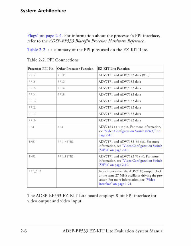
PPI Interface ........................................................................... 2-5
Video Output Mode ........................................................... 2-7
Video Input Mode .............................................................. 2-7
ADSP-BF533 EZ-KIT Lite Evaluation System Manual vii
Contents
UART Port .............................................................................. 2-7
Expansion Interface ................................................................. 2-8
JTAG Emulation Port .............................................................. 2-8
Jumper and Switch Settings ........................................................... 2-9
UART Loop Jumper (JP4) ....................................................... 2-9
Boot Mode Switch (SW11) .................................................... 2-10
Test DIP Switches (SW1 and SW2) ........................................ 2-10
Video Configuration Switch (SW3) ....................................... 2-10
Push Button Enable Switch (SW9) ......................................... 2-11
SPIS1/SPISS Select Switch (SW10) ........................................ 2-12
SPORT0 Switch (SW12) ....................................................... 2-12
LEDs and Push Buttons .............................................................. 2-12
Programmable Flag Push Buttons (SW4–7) ............................ 2-13
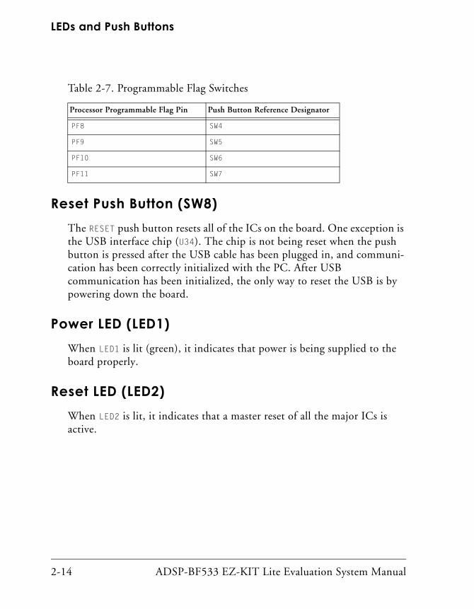
Reset Push Button (SW8) ...................................................... 2-14
Power LED (LED1) ............................................................... 2-14
Reset LED (LED2) ................................................................ 2-14
User LEDs (LED4–9) ............................................................ 2-15
USB Monitor LED (ZLED3) ................................................. 2-15
Connectors ................................................................................. 2-16
Expansion Interface (J1–3) .................................................... 2-17
Audio (J4 and J5) .................................................................. 2-17
Video (J8) ............................................................................. 2-18
Power (J9) ............................................................................. 2-18
FlashLINK (P1) .................................................................... 2-19
Contents
viii ADSP-BF533 EZ-KIT Lite Evaluation System Manual
RS-232 (P2) ......................................................................... 2-19
SPORT1 (P3) ....................................................................... 2-20
JTAG (ZP4) .......................................................................... 2-20
SPI (P6) ................................................................................ 2-21
ADSP-BF533 EZ-KIT LITE BILL OF MATERIALS
ADSP-BF533 EZ-KIT LITE SCHEMATIC
INDEX
ADSP-BF533 EZ-KIT Lite Evaluation System Manual ix
PREFACE
Thank you for purchasing the ADSP-BF533 EZ-KIT Lite®, Analog Devices, Inc. evaluation system for Blackfin® processors.
Blackfin processors embody a type of embedded processor designed specif-ically to meet the computational demands and power constraints of today’s embedded audio, video, and communications applications. They deliver breakthrough signal-processing performance and power efficiency within a reduced instruction set computing (RISC) programming model.
Blackfin processors support a media instruction set computing (MISC) architecture. This architecture is the natural merging of RISC, media functions, and digital signal processing (DSP) characteristics. Blackfin processors deliver signal-processing performance in a microprocessor-like environment.
Based on the Micro Signal Architecture (MSA), Blackfin processors com-bine a 32-bit RISC instruction set, dual 16-bit multiply accumulate (MAC) DSP functionality, and eight-bit video processing performance that had previously been the exclusive domain of very-long instruction word (VLIW) media processors.

x ADSP-BF533 EZ-KIT Lite Evaluation System Manual
The evaluation board is designed to be used in conjunction with the CrossCore® Embedded Studio (CCES) and VisualDSP++® development environments to test the capabilities of the ADSP-BF533 Blackfin proces-sors. The development environment gives you the ability to perform advanced application code development and debug, such as:
• Create, compile, assemble, and link application programs written in C++, C, and ADSP-BF533 assembly
• Load, run, step, halt, and set breakpoints in application programs
• Read and write data and program memory
• Read and write core and peripheral registers
• Plot memory
Access to the ADSP-BF533 processor from a personal computer (PC) is achieved through a USB port or an optional JTAG emulator. The USB interface gives unrestricted access to the ADSP-BF533 processor and the evaluation board peripherals. Analog Devices JTAG emulators offer faster communication between the host PC and target hardware. Analog Devices carries a wide range of in-circuit emulation products. To learn more about Analog Devices emulators and processor development tools, go to http://www.analog.com/dsp/tools.
The ADSP-BF533 EZ-KIT Lite provides example programs to demon-strate the capabilities of the evaluation board.
ADSP-BF533 EZ-KIT Lite Evaluation System Manual xi
Preface
Product OverviewThe board features:
• Analog Devices ADSP-BF533 Blackfin processor
• Performance up to 600 MHz
• 160-pin mini-BGA package
• 27 MHz CLKIN oscillator
• Synchronous dynamic random access memory (SDRAM)
• MT48LC32M16 - 64 MB (32M x 16 bits)
• Flash memories
• 2 MB (512K x 16 x 2chips)
• Analog audio interface
• AD1836 – Analog Devices 96 kHz audio codec
• 4 input RCA phono jacks (2 channels)
• 6 output RCA phono jacks (3 channels)
• Analog video interface
• ADV7183 video decoder w/ 3 input RCA phono jacks
• ADV7171 video encoder w/ 3 output RCA phono jacks
• Universal asynchronous receiver/transmitter (UART)
• ADM3202 RS-232 line driver/receiver
• DB9 male connector
Product Overview
xii ADSP-BF533 EZ-KIT Lite Evaluation System Manual
• LEDs
• 10 LEDs: 1 power (green), 1 board reset (red), 1 USB (red), 6 general-purpose (amber), and 1 USB monitor (amber)
• Push buttons
• 5 push buttons with debounce logic: 1 reset, 4 programmable flags
• Expansion interface
• PPI, SPI, EBIU, Timers2-0, UART, programmable flags, SPORT0, SPORT1
• Other features
• JTAG ICE 14-pin header
The EZ-KIT Lite board has two flash memories with a total of 2 MB of memory. The flash memories can be used to store user-specific boot code, allowing the board to run as a stand-alone unit. For more information, see “Flash Memory” on page 1-15. The board also has 64 MB of SDRAM, which can be used by the user at runtime.
SPORTs interface with the AD1836 audio codec to aid development of audio signal processing applications. SPORT0 also attaches to an off-board connector for communication with other serial devices. For information about SPORT0, see “SPORT Audio Interface” on page 2-3.
The parallel peripheral interface (PPI) of the processor connects to both a video encoder and video decoder, facilitating development of video signal processing applications.
The UART of the processor connects to an RS-232 line driver and a DB9 male connector, providing an interface to a PC or other serial device.
Additionally, the EZ-KIT Lite board provides access to most of the pro-cessor’s peripheral ports. Access is provided in the form of a
ADSP-BF533 EZ-KIT Lite Evaluation System Manual xiii
Preface
three-connector expansion interface. For information about the expansion interface, see “Expansion Interface” on page 2-8.
Purpose of This ManualThe ADSP-BF533 EZ-KIT Lite Evaluation System Manual provides instructions for installing the product hardware (board). The text describes the operation and configuration of the board components and provides guidelines for running your own code on the ADSP-BF533 EZ-KIT Lite. Finally, a schematic and a bill of materials are provided as a reference for future designs.
Intended AudienceThe primary audience for this manual is a programmer who is familiar with Analog Devices processors. This manual assumes that the audience has a working knowledge of the appropriate processor architecture and instruction set.
Programmers who are unfamiliar with Analog Devices processors can use this manual but should supplement it with other texts that describe your target architecture. For the locations of these documents, see “Related Documents”.
Programmers who are unfamiliar with CCES or VisualDSP++ should refer to the online help and user’s manuals.
Manual Contents
xiv ADSP-BF533 EZ-KIT Lite Evaluation System Manual
Manual ContentsThe manual consists of:
• Chapter 1, “Using the ADSP-BF533 EZ-KIT Lite” on page 1-1Describes the EZ-KIT Lite functionality from a programmer’s per-spective and provides an easy-to-access memory map.
• Chapter 2, “ADSP-BF533 EZ-KIT Lite Hardware Reference” on page 2-1Provides information on the EZ-KIT Lite hardware components.
• Appendix A, “ADSP-BF533 EZ-KIT Lite Bill Of Materials” on page A-1Provides a list of components used to manufacture the EZ-KIT Lite board.
• Appendix B, “ADSP-BF533 EZ-KIT Lite Schematic” on page B-1Provides the resources to allow board-level debugging or to use as a reference design. Appendix B is part of the online help.
What’s New in This ManualThis is revision 3.2 of the ADSP-BF533 EZ-KIT Lite Evaluation System Manual. The manual has been updated to include CCES information. Additional changes include the following.
• The “Configuring Flash Memory” section has been updated to reflect obsoleted flash memory devices.
• Modifications and corrections based on errata reports against the previous manual revision have been made.
For the latest version of this manual, please refer to the Analog Devices Web site.
ADSP-BF533 EZ-KIT Lite Evaluation System Manual xv
Preface
Technical SupportYou can reach Analog Devices processors and DSP technical support in the following ways:
• Post your questions in the processors and DSP support community at EngineerZone®:http://ez.analog.com/community/dsp
• Submit your questions to technical support directly at:http://www.analog.com/support
• E-mail your questions about processors, DSPs, and tools develop-ment software from CrossCore Embedded Studio or VisualDSP++:
Choose Help > Email Support. This creates an e-mail [email protected] and automatically attaches your CrossCore Embedded Studio or VisualDSP++ version infor-mation and license.dat file.
• E-mail your questions about processors and processor applications to: [email protected] [email protected] (Greater China support)
• In the USA only, call 1-800-ANALOGD (1-800-262-5643)
• Contact your Analog Devices sales office or authorized distributor. Locate one at:www.analog.com/adi-sales
Supported Processors
xvi ADSP-BF533 EZ-KIT Lite Evaluation System Manual
• Send questions by mail to:Processors and DSP Technical SupportAnalog Devices, Inc.Three Technology WayP.O. Box 9106Norwood, MA 02062-9106USA
Supported ProcessorsThis evaluation system supports Analog Devices ADSP-BF533 Blackfin embedded processors.
Product InformationProduct information can be obtained from the Analog Devices Web site and the online help system.
Analog Devices Web SiteThe Analog Devices Web site, www.analog.com, provides information about a broad range of products—analog integrated circuits, amplifiers, converters, and digital signal processors.
To access a complete technical library for each processor family, go to http://www.analog.com/processors/technical_library. The manuals selection opens a list of current manuals related to the product as well as a link to the previous revisions of the manuals. When locating your manual title, note a possible errata check mark next to the title that leads to the current correction report against the manual.
Also note, myAnalog is a free feature of the Analog Devices Web site that allows customization of a Web page to display only the latest information
ADSP-BF533 EZ-KIT Lite Evaluation System Manual xvii
Preface
about products you are interested in. You can choose to receive weekly e-mail notifications containing updates to the Web pages that meet your interests, including documentation errata against all manuals. myAnalog provides access to books, application notes, data sheets, code examples, and more.
Visit myAnalog to sign up. If you are a registered user, just log on. Your user name is your e-mail address.
EngineerZoneEngineerZone is a technical support forum from Analog Devices. It allows you direct access to ADI technical support engineers. You can search FAQs and technical information to get quick answers to your embedded processing and DSP design questions.
Use EngineerZone to connect with other DSP developers who face similar design challenges. You can also use this open forum to share knowledge and collaborate with the ADI support team and your peers. Visit http://ez.analog.com to sign up.
Related Documents
xviii ADSP-BF533 EZ-KIT Lite Evaluation System Manual
Related DocumentsFor additional information about the product, refer to the following publications.
Notation ConventionsText conventions used in this manual are identified and described as follows.
Table 1. Related Processor Publications
Title Description
ADSP-BF531/ADSP-BF532/ADSP-BF533 Blackfin Embedded Processor Data Sheet
General functional description, pinout, and timing of the processor
ADSP-BF533 Blackfin Processor Hardware Reference
Description of the internal processor architec-ture and all register functions
Blackfin Processor Programming Reference Description of all allowed processor assembly instructions
Example Description
Close command (File menu)
Titles in reference sections indicate the location of an item within the development environment’s menu system (for example, the Close com-mand appears on the File menu).
{this | that} Alternative required items in syntax descriptions appear within curly brackets and separated by vertical bars; read the example as this or that. One or the other is required.
[this | that] Optional items in syntax descriptions appear within brackets and sepa-rated by vertical bars; read the example as an optional this or that.
[this,…] Optional item lists in syntax descriptions appear within brackets delim-ited by commas and terminated with an ellipse; read the example as an optional comma-separated list of this.
.SECTION Commands, directives, keywords, and feature names are in text with letter gothic font.
ADSP-BF533 EZ-KIT Lite Evaluation System Manual xix
Preface
filename Non-keyword placeholders appear in text with italic style format.
Note: For correct operation, ...A Note provides supplementary information on a related topic. In the online version of this book, the word Note appears instead of this
symbol.
Caution: Incorrect device operation may result if ...Caution: Device damage may result if ... A Caution identifies conditions or inappropriate usage of the product that could lead to undesirable results or product damage. In the online version of this book, the word Caution appears instead of this symbol.
Warning: Injury to device users may result if ... A Warning identifies conditions or inappropriate usage of the product that could lead to conditions that are potentially hazardous for the devices users. In the online version of this book, the word Warning appears instead of this symbol.
Example Description
Notation Conventions
xx ADSP-BF533 EZ-KIT Lite Evaluation System Manual
ADSP-BF533 EZ-KIT Lite Evaluation System Manual 1-1
1 USING THE ADSP-BF533 EZ-KIT LITE
This chapter provides specific information to assist you with development of programs for the ADSP-BF533 EZ-KIT Lite evaluation system.
The information appears in the following sections.
• “Package Contents” on page 1-3Lists the items contained in your ADSP-BF533 EZ-KIT Lite package.
• “Default Configuration” on page 1-3Shows the default configuration of the ADSP-BF533 EZ-KIT Lite.
• “CCES Install and Session Startup” on page 1-5Instructs how to start a new or open an existing ADSP-BF533 EZ-KIT Lite session using CCES.
• “VisualDSP++ Install and Session Startup” on page 1-9Instructs how to start a new or open an existing ADSP-BF533 EZ-KIT Lite session using VisualDSP++.
• “CCES Evaluation License” on page 1-10Describes the CCES demo license shipped with the EZ-KIT Lite.
• “VisualDSP++ Evaluation License” on page 1-11Describes the VisualDSP++ demo license shipped with the EZ-KIT Lite.
• “Memory Map” on page 1-12Defines the ADSP-BF533 EZ-KIT Lite board’s memory map.
1-2 ADSP-BF533 EZ-KIT Lite Evaluation System Manual
• “SDRAM Interface” on page 1-13·Defines the register values to configure the on-board SDRAM.
• “Flash Memory” on page 1-15Describes the on-board flash memory.
• “LEDs and Push Buttons” on page 1-19Describes the board’s general-purpose IO pins and buttons.
• “Audio Interface” on page 1-20Describes the board’s audio interface.
• “Video Interface” on page 1-21Describes the board’s video interface.
• “Board Design Database” on page 1-22Provides information about board design.
• “Example Programs” on page 1-22Provides information about the example programs included in the ADSP-BF533 EZ-KIT Lite evaluation system.
For information on the graphical user interface, including the boot load-ing, target options, and other facilities of the EZ-KIT Lite system, refer to the online help.
For more detailed information about programming the ADSP-BF533 Blackfin processor, see the documents referred to at “Related Documents”.
ADSP-BF533 EZ-KIT Lite Evaluation System Manual 1-3
Using the ADSP-BF533 EZ-KIT Lite
Package ContentsYour ADSP-BF533 EZ-KIT Lite evaluation system package contains the following items.
• ADSP-BF533 EZ-KIT Lite board
• Universal 7.5V DC power supply
• USB 2.0 type cable
If any item is missing, contact the vendor where you purchased your EZ-KIT Lite or contact Analog Devices, Inc.
Default Configuration
The ADSP-BF533 EZ-KIT Lite board is designed to run outside your per-sonal computer as a standalone unit.
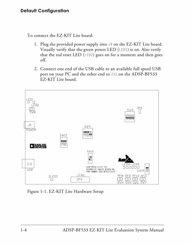
When removing the EZ-KIT Lite board from the package, handle the board carefully to avoid the discharge of static electricity, which may dam-age some components. Figure 1-1 shows the default jumper settings, DIP switch, connector locations, and LEDs used in installation. Confirm that your board is set up in the default configuration before using the board.
The EZ-KIT Lite evaluation system contains ESD (electrostatic dis-charge) sensitive devices. Electrostatic charges readily accumulate on the human body and equipment and can discharge without detection. Perma-nent damage may occur on devices subjected to high-energy discharges. Proper ESD precautions are recommended to avoid performance degrada-tion or loss of functionality. Store unused EZ-KIT Lite boards in the pro-tective shipping package.
Default Configuration
1-4 ADSP-BF533 EZ-KIT Lite Evaluation System Manual
To connect the EZ-KIT Lite board:
1. Plug the provided power supply into J9 on the EZ-KIT Lite board. Visually verify that the green power LED (LED1) is on. Also verify that the red reset LED (LED2) goes on for a moment and then goes off.
2. Connect one end of the USB cable to an available full speed USB port on your PC and the other end to ZJ1 on the ADSP-BF533 EZ-KIT Lite board.
Figure 1-1. EZ-KIT Lite Hardware Setup
ADSP-BF533 EZ-KIT Lite Evaluation System Manual 1-5
Using the ADSP-BF533 EZ-KIT Lite
CCES Install and Session StartupFor information about CCES and to download the software, go to www.analog.com/CCES. A link for the ADSP-BF533 EZ-KIT Lite Board Support Package (BSP) for CCES can be found at http://www.analog.com/Blackfin/EZKits.
Follow these instructions to ensure correct operation of the product soft-ware and hardware.
Step 1: Connect the EZ-KIT Lite board to a personal computer (PC) run-ning CCES using one of two options: an Analog Devices emulator or via the debug agent.
Using an Emulator:
1. Plug one side of the USB cable into the USB connector of the emu-lator. Plug the other side into a USB port of the PC running CCES.
2. Attach the emulator to the header connector ZP4 (labeled JTAG) on the EZ-KIT Lite board.
Using the on-board Debug Agent:
1. Plug one side of the USB cable into the USB connector ZJ1 (labeled USB) on the EZ-KIT Lite board.
2. Plug the other side of the cable into a USB port of the PC running CCES.
CCES Install and Session Startup
1-6 ADSP-BF533 EZ-KIT Lite Evaluation System Manual
Step 2: Attach the provided cord and appropriate plug to the 7.5V power adaptor.
1. Plug the jack-end of the power adaptor into the power connector J9 (labeled POWER) on the EZ-KIT Lite board.
2. Plug the other side of the power adaptor into a power outlet. The power LED (labeled LED1) is lit green when power is applied to the board.
3. Power the emulator (if used). Plug the jack-end of the assembled power adaptor into the emulator and plug the other side of the power adaptor into a power outlet. The enable/power indicator is lit green when power is applied.
Step 3 (if connected through the debug agent): Verify that the yellow USB monitor LED (labeled ZLED3) on the debug agent is on. This signifies that the board is communicating properly with the host PC and ready to run CCES.
Session StartupIt is assumed that the CrossCore Embedded Studio software is installed and running on your PC.
Note: If you connect the board or emulator first (before installing CCES) to the PC, the Windows driver wizard may not find the board drivers.
1. Navigate to the CCES environment via the Start menu.
Note that CCES is not connected to the target board.
ADSP-BF533 EZ-KIT Lite Evaluation System Manual 1-7
Using the ADSP-BF533 EZ-KIT Lite
2. Use the system configuration utility to connect to the EZ-KIT Lite board.
If a debug configuration exists already, select the appropriate configuration and click Apply and Debug or Debug. Go to step 8.
To create a debug configuration, do one of the following:
• Click the down arrow next to the little bug icon, select Debug Configurations
• Choose Run > Debug Configurations.
The Debug Configuration dialog box appears.
3. Select CrossCore Embedded Studio Application and click (New launch configuration).
The Select Processor page of the Session Wizard appears.
4. Ensure Blackfin is selected in Processor family. In Processor type, select ADSP-BF533. Click Next.
The Select Connection Type page of the Session Wizard appears.
5. Select one of the following:
• For standalone debug agent connections, EZ-KIT Lite and click Next.
• For emulator connections, Emulator and click Next.
The Select Platform page of the Session Wizard appears.
CCES Install and Session Startup
1-8 ADSP-BF533 EZ-KIT Lite Evaluation System Manual
6. Do one of the following:
• For standalone debug agent connections, ensure that the selected platform is ADSP-BF533 EZ-KIT Lite via Debug Agent.
• For emulator connections, choose the type of emulator that is connected to the board.
7. Click Finish to close the wizard.
The new debug configuration is created and added to the pro-gram(s) to load list.
8. In the Program(s) to load section, choose the program to load when connecting to the board. If not loading any program upon connection to the target, do not make any changes.
Note that while connected to the target, there is no way to choose a program to download. To load a program once connected, termi-nate the session.
To delete a configuration, go to the Debug Configurations dialog box and select the configuration to delete. Click and choose Yes when asked if you wish to delete the selected launch configuration. Then Close the dialog box.
To disconnect from the target board, click the terminate button (red box) or choose Run > Terminate.
To delete a session, choose Target > Session > Session List. Select the session name from the list and click Delete. Click OK.
ADSP-BF533 EZ-KIT Lite Evaluation System Manual 1-9
Using the ADSP-BF533 EZ-KIT Lite
VisualDSP++ Install and Session StartupFor information about VisualDSP++ and to download the software, go to www.analog.com/VisualDSP.
1. Verify that the yellow USB monitor LED (ZLED3, located near the USB connector) is lit. This signifies that the board is communicat-ing properly with the host PC and is ready to run VisualDSP++.
2. If you are running VisualDSP++ for the first time, navigate to the VisualDSP++ environment via the Start > Programs menu. The main window appears. Note that VisualDSP++ does not connect to any session. Skip the rest of this step to step 3.
If you have run VisualDSP++ previously, the last opened session appears on the screen. You can override the default behavior and force VisualDSP++ to start a new session by pressing and holding down the Ctrl key while starting VisualDSP++. Do not release the Ctrl key until the Session Wizard appears on the screen. Go to step 4.
3. To connect to a new EZ-KIT Lite session, start Session Wizard by selecting one of the following.
• From the Session menu, New Session.
• From the Session menu, Session List. Then click New Session from the Session List dialog box.
• From the Session menu, Connect to Target.
4. The Select Processor page of the wizard appears on the screen.Ensure Blackfin is selected in Processor family. In Choose a target processor, select ADSP-BF533. Click Next.
5. The Select Connection Type page of the wizard appears on the screen. Select EZ-KIT Lite and click Next.

CCES Evaluation License
1-10 ADSP-BF533 EZ-KIT Lite Evaluation System Manual
6. The Select Platform page of the wizard appears on the screen. Ensure that the selected platform is ADSP-BF533 EZ-KIT Lite via Debug Agent. Specify your own Session name for your session or accept the default name.
The session name can be a string of any length; although, the box displays approximately 32 characters. The session name can include space characters. If you do not specify a session name, VisualDSP++ creates a session name by combining the name of the selected platform with the selected processor. The only way to change a session name later is to delete the session and open a new session.
Click Next.
7. The Finish page of the wizard appears on the screen. The page dis-plays your selections.Check the selections. If you are not satisfied, click Back to make changes; otherwise, click Finish. VisualDSP++ creates the new session and connects to the EZ-KIT Lite. Once connected, the main window’s title is changed to include the ses-sion name set in step 6.
To disconnect from a session, click the disconnect button or select Session > Disconnect from Target.
To delete a session, select Session > Session List. Select the session name from the list and click Delete. Click OK.
CCES Evaluation LicenseThe ADSP-BF533 EZ-KIT Lite software is part of the Board Support Package (BSP) for the Blackfin ADSP-BF53x family. The EZ-KIT Lite is a licensed product that offers an unrestricted evaluation license for 90 days after activation. Once the evaluation period ends, the evaluation license
ADSP-BF533 EZ-KIT Lite Evaluation System Manual 1-11
Using the ADSP-BF533 EZ-KIT Lite
becomes permanently disabled. If the evaluation license is installed but not activated, it allows 10 days of unrestricted use and then becomes dis-abled. The license can be re-enabled by activation.
An evaluation license can be upgraded to a full license. Licenses can be purchased from:
• Analog Devices directly. Call (800) 262-5645 or 781-937-2384 or go to: http://www.analog.com/buyonline.
• Analog Devices, Inc. local sales office or authorized distributor. To locate one, go to:http://www.analog.com/salesdir/continent.asp.
The EZ-KIT Lite hardware must be connected and powered up to use CCES with a valid evaluation or full license.
VisualDSP++ Evaluation LicenseThe ADSP-BF533 EZ-KIT Lite installation is part of the VisualDSP++ installation. The EZ-KIT Lite is a licensed product that offers an unre-stricted evaluation license for the first 90 days. Once the initial unrestricted 90-day evaluation license expires:
• VisualDSP++ allows a connection to the ADSP-BF533 EZ-KIT Lite via the USB debug agent interface only. Connections to simu-lators and emulation products are no longer allowed.
• The linker restricts a user’s program to 20 KB of memory for code space with no restrictions for data space.
To avoid errors when opening VisualDSP++, the EZ-KIT Lite hardware must be connected and powered up. This is true for using VisualDSP++ with a valid evaluation or full license.
Memory Map
1-12 ADSP-BF533 EZ-KIT Lite Evaluation System Manual
Memory MapThe ADSP-BF533 processor has internal SRAM that can be used for instruction or data storage. The configuration of internal SRAM is detailed in the ADSP-BF533 Processor Hardware Reference.
The ADSP-BF533 EZ-KIT Lite board includes two types of external memory, SDRAM and flash memory.
The size of the SDRAM is 64 Mbytes (32M x 16-bits). The processor’s memory select pin SMS0 is configured for the SDRAM.
The flash memory is implemented with two dual-bank flash memory devices. These devices include primary and secondary flash memory as well as internal SRAM and registers. Primary flash memory totals 2 Mbytes mapped into two separate asynchronous memory banks, 1 Mbyte each. Secondary flash memory, along with SRAM and registers, occupies the third bank of asynchronous memory space. The processor’s AMS0, AMS1, and AMS2 memory select pins are used for that purpose.
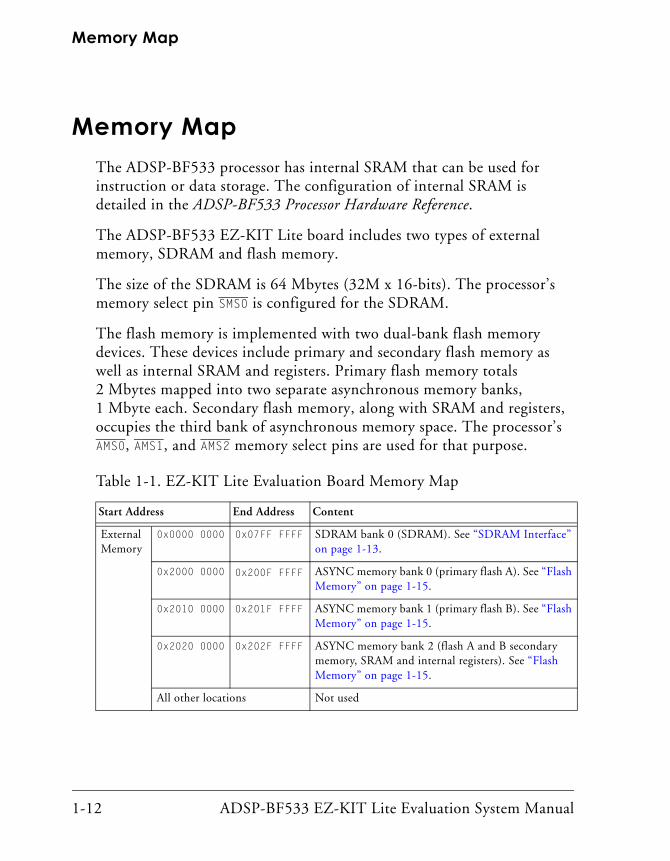
Table 1-1. EZ-KIT Lite Evaluation Board Memory Map
Start Address End Address Content
External Memory
0x0000 0000 0x07FF FFFF SDRAM bank 0 (SDRAM). See “SDRAM Interface” on page 1-13.
0x2000 0000 0x200F FFFF ASYNC memory bank 0 (primary flash A). See “Flash Memory” on page 1-15.
0x2010 0000 0x201F FFFF ASYNC memory bank 1 (primary flash B). See “Flash Memory” on page 1-15.
0x2020 0000 0x202F FFFF ASYNC memory bank 2 (flash A and B secondary memory, SRAM and internal registers). See “Flash Memory” on page 1-15.
All other locations Not used
ADSP-BF533 EZ-KIT Lite Evaluation System Manual 1-13
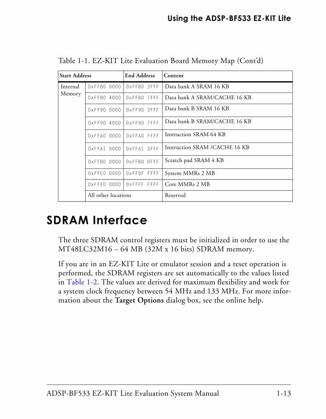
Using the ADSP-BF533 EZ-KIT Lite
SDRAM InterfaceThe three SDRAM control registers must be initialized in order to use the MT48LC32M16 – 64 MB (32M x 16 bits) SDRAM memory.
If you are in an EZ-KIT Lite or emulator session and a reset operation is performed, the SDRAM registers are set automatically to the values listed in Table 1-2. The values are derived for maximum flexibility and work for a system clock frequency between 54 MHz and 133 MHz. For more infor-mation about the Target Options dialog box, see the online help.
Internal Memory
0xFF80 0000 0xFF80 3FFF Data bank A SRAM 16 KB
0xFF80 4000 0xFF80 7FFF Data bank A SRAM/CACHE 16 KB
0xFF90 0000 0xFF90 3FFF Data bank B SRAM 16 KB
0xFF90 4000 0xFF90 7FFF Data bank B SRAM/CACHE 16 KB
0xFFA0 0000 0xFFA0 FFFF Instruction SRAM 64 KB
0xFFA1 0000 0xFFA1 3FFF Instruction SRAM /CACHE 16 KB
0xFFB0 0000 0xFFBO 0FFF Scratch pad SRAM 4 KB
0xFFC0 0000 0xFFDF FFFF System MMRs 2 MB
0xFFE0 0000 0xFFFF FFFF Core MMRs 2 MB
All other locations Reserved
Table 1-1. EZ-KIT Lite Evaluation Board Memory Map (Cont’d)
Start Address End Address Content
SDRAM Interface
1-14 ADSP-BF533 EZ-KIT Lite Evaluation System Manual
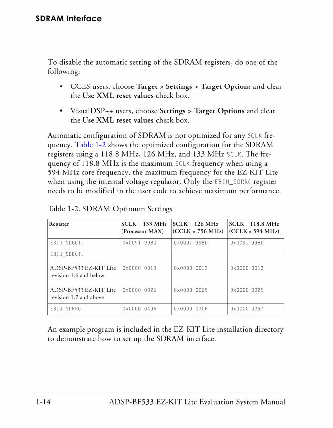
To disable the automatic setting of the SDRAM registers, do one of the following:
• CCES users, choose Target > Settings > Target Options and clear the Use XML reset values check box.
• VisualDSP++ users, choose Settings > Target Options and clear the Use XML reset values check box.
Automatic configuration of SDRAM is not optimized for any SCLK fre-quency. Table 1-2 shows the optimized configuration for the SDRAM registers using a 118.8 MHz, 126 MHz, and 133 MHz SCLK. The fre-quency of 118.8 MHz is the maximum SCLK frequency when using a 594 MHz core frequency, the maximum frequency for the EZ-KIT Lite when using the internal voltage regulator. Only the EBIU_SDRRC register needs to be modified in the user code to achieve maximum performance.
An example program is included in the EZ-KIT Lite installation directory to demonstrate how to set up the SDRAM interface.
Table 1-2. SDRAM Optimum Settings
Register SCLK = 133 MHz(Processor MAX)
SCLK = 126 MHz(CCLK = 756 MHz)
SCLK = 118.8 MHz(CCLK = 594 MHz)
EBIU_SDGCTL 0x0091 998D 0x0091 998D 0x0091 998D
EBIU_SDBCTL
ADSP-BF533 EZ-KIT Literevision 1.6 and below
ADSP-BF533 EZ-KIT Literevision 1.7 and above
0x0000 0013
0x0000 0025
0x0000 0013
0x0000 0025
0x0000 0013
0x0000 0025
EBIU_SDRRC 0x0000 0406 0x0000 03CF 0x0000 0397
ADSP-BF533 EZ-KIT Lite Evaluation System Manual 1-15
Using the ADSP-BF533 EZ-KIT Lite
Flash MemoryThe following sections describe how to use the memory and general-pur-pose IO pins, as well as how to configure the flash memory devices.
The ADSP-BF533 EZ-KIT Lite board employs two PSD4256G6V flash general-purpose IO devices from STMicroelectronics. These devices not only have flash memory but also extra IO pins, which are memory mapped.
Example code is provided in the EZ-KIT Lite installation directory to demonstrate how to program the flash memory as well as to demonstrate the functionality of the general-purpose IO pins.
Flash Memory MapEach device includes the following memory segments:
• 1M byte of primary flash memory
• 64K bytes of secondary flash memory
• 32 Kbytes of internal SRAM
• 256 Bytes of configuration registers (IO control)
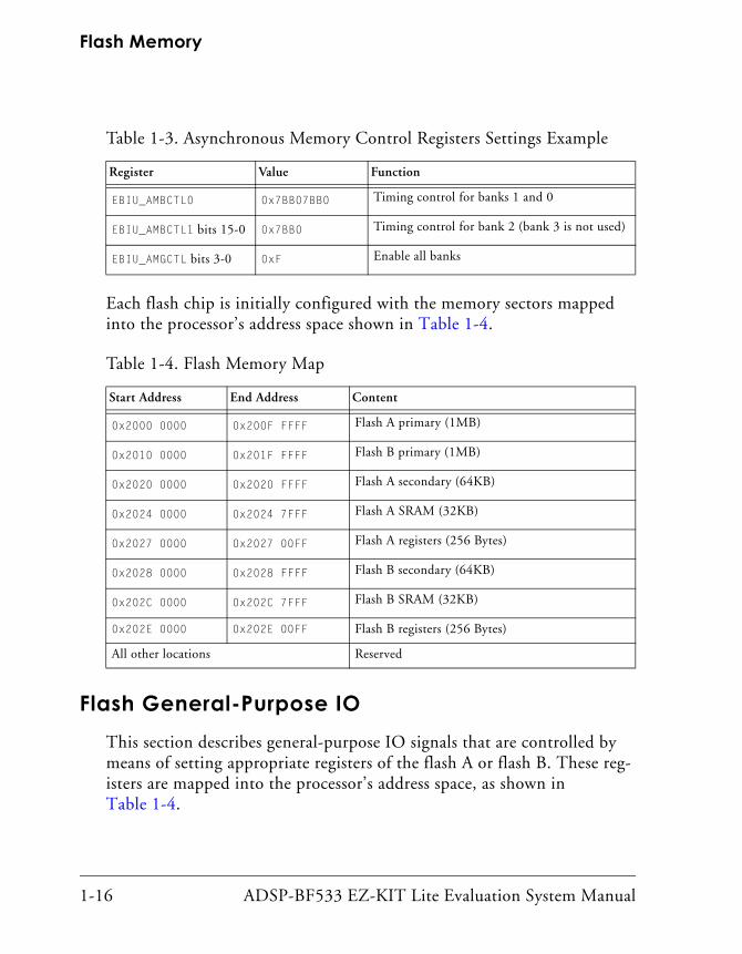
Access to each segment can be 8-bit or 16-bit. The processor’s AMS0, AMS1, and AMS2 memory select pin are used for that purpose. Asynchronous memory bank 0 is always enabled after a hard reset, while banks 1 and 2 need to be enabled by software. Table 1-3 provides an example on asyn-chronous memory configuration registers.
Flash Memory
1-16 ADSP-BF533 EZ-KIT Lite Evaluation System Manual
Each flash chip is initially configured with the memory sectors mapped into the processor’s address space shown in Table 1-4.
Flash General-Purpose IOThis section describes general-purpose IO signals that are controlled by means of setting appropriate registers of the flash A or flash B. These reg-isters are mapped into the processor’s address space, as shown in Table 1-4.
Table 1-3. Asynchronous Memory Control Registers Settings Example
Register Value Function
EBIU_AMBCTL0 0x7BB07BB0 Timing control for banks 1 and 0
EBIU_AMBCTL1 bits 15-0 0x7BB0 Timing control for bank 2 (bank 3 is not used)
EBIU_AMGCTL bits 3-0 0xF Enable all banks
Table 1-4. Flash Memory Map
Start Address End Address Content
0x2000 0000 0x200F FFFF Flash A primary (1MB)
0x2010 0000 0x201F FFFF Flash B primary (1MB)
0x2020 0000 0x2020 FFFF Flash A secondary (64KB)
0x2024 0000 0x2024 7FFF Flash A SRAM (32KB)
0x2027 0000 0x2027 00FF Flash A registers (256 Bytes)
0x2028 0000 0x2028 FFFF Flash B secondary (64KB)
0x202C 0000 0x202C 7FFF Flash B SRAM (32KB)
0x202E 0000 0x202E 00FF Flash B registers (256 Bytes)
All other locations Reserved
ADSP-BF533 EZ-KIT Lite Evaluation System Manual 1-17
Using the ADSP-BF533 EZ-KIT Lite
Flash device IO pins are arranged as 8-bit ports labeled A through G. There is a set of 8-bit registers associated with each port. These registers are Direction, Data In, and Data Out. Note that the Direction and Data Out registers are cleared to all zeros at power-up or hardware reset.
The Direction register controls IO pins direction. When a bit is 0, a cor-responding pin functions as an input. When the bit is 1, a corresponding pin is an output. This is a 8-bit read-write register.
The Data In register allows reading the status of port’s pins. This is a 8-bit read-only register.
The Data Out register allows clearing an output pin to 0 or setting it to 1. This is a 8-bit read-write register.
The ADSP-BF533 EZ-KIT Lite board employs only flash A and flash B ports A and B. Table 1-5 and Table 1-6 provide configuration register addresses for flash A and flash B, respectively (only ports A and B are listed). The following bits connect to the expansion board connector.
• Flash A: port A bits 7 and 6, as well as port B bits 7 and 6
• Flash B: port A bits 7–0
Table 1-5. Flash A Configuration Registers for Ports A and B
Register Name Port A Address Port B Address
Data In (read-only) 0x2027 0000 0x2027 0001
Data Out (read-write) 0x2027 0004 0x2027 0005
Direction (read-write) 0x2027 0006 0x2027 0007
Flash Memory
1-18 ADSP-BF533 EZ-KIT Lite Evaluation System Manual
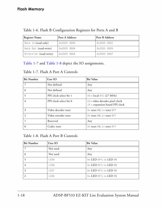
Table 1-7 and Table 1-8 depict the IO assignments.
Table 1-6. Flash B Configuration Registers for Ports A and B
Register Name Port A Address Port B Address
Data In (read-only) 0x202E 0000 0x202E 0001
Data Out (read-write) 0x202E 0004 0x202E 0005
Direction (read-write) 0x202E 0006 0x202E 0007
Table 1-7. Flash A Port A Controls
Bit Number User IO Bit Value
7 Not defined Any
6 Not defined Any
5 PPI clock select bit 1 00 = local OSC (27 MHz)
4 PPI clock select bit 0 01= video decoder pixel clock1X = expansion board PPI clock
3 Video decoder reset 0= reset ON; 1= reset OFF
2 Video encoder reset 0= reset ON; 1= reset OFF
1 Reserved Any
0 Codec reset 0= reset ON; 1= reset OFF
Table 1-8. Flash A Port B Controls
Bit Number User IO Bit Value
7 Not used Any
6 Not used Any
5 LED9 0= LED OFF; 1= LED ON
4 LED8 0= LED OFF; 1= LED ON
3 LED7 0= LED OFF; 1= LED ON
2 LED6 0= LED OFF; 1= LED ON
ADSP-BF533 EZ-KIT Lite Evaluation System Manual 1-19
Using the ADSP-BF533 EZ-KIT Lite
Configuring Flash MemoryThe PSD4256G6V flash memory devices used on the ADSP-BF533 EZ-KIT Lite have been obsoleted by ST Microelectronics and are no lon-ger available for purchase. The software and programming adapter to reconfigure these devices has also been obsoleted and is no longer available.
LEDs and Push ButtonsThe EZ-KIT Lite provides four push buttons and six LEDs for gen-eral-purpose IO.
The six LEDs, labeled LED4 through LED9, are accessed via some of the general-purpose IO pins of the flash memory interface. For information on how to program the pins, see “Flash General-Purpose IO” on page 1-16.
The four general-purpose push button are labeled SW4 through SW7. A sta-tus of each individual button can be read through programmable flag (PF) inputs, PF8 through PF11. A PF reads 1 when a corresponding switch is being pressed-on. When the switch is released, the PF reads 0. A connec-tion between the push button and PF input is established through the SW9 DIP switch. See “Push Button Enable Switch (SW9)” on page 2-11 for details.
An example program is included in the EZ-KIT Lite installation directory to demonstrate the functionality of the LEDs and push buttons.
1 LED5 0= LED OFF; 1= LED ON
0 LED4 0= LED OFF; 1= LED ON
Table 1-8. Flash A Port B Controls (Cont’d)
Bit Number User IO Bit Value
Audio Interface
1-20 ADSP-BF533 EZ-KIT Lite Evaluation System Manual
Audio InterfaceThe AD1836 audio codec provides three channels of stereo audio output and two channels of multichannel 96 kHz input. The SPORT0 interface of the processor links with the stereo audio data input and output pins of the AD1836 codec. The processor is capable of transferring data to the audio codec in time-division multiplexed (TDM) or two-wire interface (TWI) mode.
The TWI mode allows the codec to operate at a 96 kHz sample rate but limits the output channels to two. The TDM mode can operate at a maxi-mum of 48 kHz sample rate but allows simultaneous use of all input and output channels. When using TWI mode, the TSCLK0 and RSCLK0 pins, as well as the TFS0 and RFS0 pins of the processor, must be tied together external to the processor. This is accomplished with the SW9 DIP switch (see “Push Button Enable Switch (SW9)” on page 2-11 for more information).
The AD1836 audio codec’s internal configuration registers are configured using the SPI port of the processor. The processor’s PF4 programmable flag pin is used as the select for this device. For information on how to configure the multichannel codec, go to AD1836A.
The general-purpose IO pin PA0 of flash A is a source for the AD1836 codec reset. See “Flash General-Purpose IO” on page 1-16 for more infor-mation about the pin.
Example programs are included in the EZ-KIT Lite installation directory to demonstrate AD1836 codec capabilities.

ADSP-BF533 EZ-KIT Lite Evaluation System Manual 1-21
Using the ADSP-BF533 EZ-KIT Lite
Video InterfaceThe board supports video input and output applications. The ADV7171 video encoder provides up to three output channels of analog video, while the ADV7183 video decoder provides up to three input channels of analog video. Both the encoder and the decoder connect to the parallel peripheral interface (PPI) of the processor. For additional information on the video interface hardware, refer to “PPI Interface” on page 2-5.
For the video interface to be operational, the following basic steps must be performed.
1. Configure the SW3 DIP switch as required by the application. Refer to “Video Configuration Switch (SW3)” on page 2-10 for details.
2. Remove reset to the video device. Refer to “Flash General-Purpose IO” on page 1-16 for details.
3. If using the decoder:
• Enable device by driving programmable flag output PF2 to 0.
• Select PPI clock (see Table 1-7 on page 1-18).
4. Program internal registers of the video device in use. Both video encoder and decoder use a two-wire serial interface to access inter-nal registers. A programmable flag PF0 functions as a serial clock (SCL), and PF1 functions as a serial data (SDAT).
5. Program the processor’s PPI interface (configuration registers, DMA, etc.).
Example programs are included in the EZ-KIT Lite installation directory to demonstrate the capabilities of the video interface.
Board Design Database
1-22 ADSP-BF533 EZ-KIT Lite Evaluation System Manual
Board Design DatabaseA .zip file containing all of the electronic information required for the design, layout, fabrication and assembly of the product is available for download from the Analog Devices board design database at:http://www.analog.com/board-design-database.
Example ProgramsExample programs are provided with the ADSP-BF533 EZ-KIT Lite to demonstrate various capabilities of the product. The programs are included in the product installation kit and can be found in the Examples folder of the installation. Refer to a readme file provided with each exam-ple for more information.
CCES users are encouraged to use the example browser to find examples included with the EZ-KIT Lite Board Support Package.
ADSP-BF533 EZ-KIT Lite Evaluation System Manual 2-1
2 ADSP-BF533 EZ-KIT LITE HARDWARE REFERENCE
This chapter describes the hardware design of the ADSP-BF533 EZ-KIT Lite board. The following topics are covered.
• “System Architecture” on page 2-2Describes the configuration of the ADSP-BF533 EZ-KIT Lite board and explains how the board components interface with the processor.
• “Jumper and Switch Settings” on page 2-9Shows the location and describes the function of the configuration jumpers and switches.
• “LEDs and Push Buttons” on page 2-12Shows the location and describes the function of the LEDs and push buttons.
• “Connectors” on page 2-16Shows the location and gives the part number for all of the connec-tors on the board. Also, the manufacturer and part number information is given for the mating parts.
System Architecture
2-2 ADSP-BF533 EZ-KIT Lite Evaluation System Manual
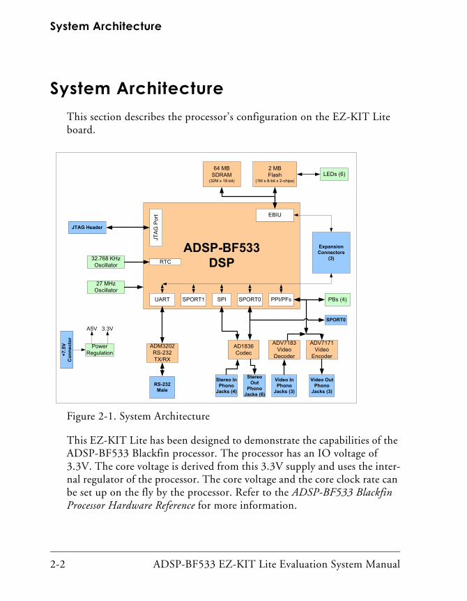
System ArchitectureThis section describes the processor’s configuration on the EZ-KIT Lite board.
This EZ-KIT Lite has been designed to demonstrate the capabilities of the ADSP-BF533 Blackfin processor. The processor has an IO voltage of 3.3V. The core voltage is derived from this 3.3V supply and uses the inter-nal regulator of the processor. The core voltage and the core clock rate can be set up on the fly by the processor. Refer to the ADSP-BF533 Blackfin Processor Hardware Reference for more information.
Figure 2-1. System Architecture
ADSP-BF533DSP
AD1836 Codec
JTAG Header
Power Regulation
LEDs (6)
EBIU
JTA
G P
ort
A5V
+7.5
VC
onne
ctor
32.768 KHz Oscillator RTC
SPI
64 MB SDRAM
(32M x 16-bit)
Expansion Connectors
(3)
2 MBFlash
(1M x 8-bit x 2-chips)
27 MHz Oscillator
ADV7183Video
Decoder
ADV7171Video
Encoder
Video Out Phono
Jacks (3)
Video In Phono
Jacks (3)
3.3V
StereoOut
Phono Jacks (6)
Stereo In Phono
Jacks (4)
UART SPORT1 PBs (4)
RS-232Male
ADM3202RS-232 TX/RX
SPORT0 PPI/PFs
SPORT0
ADSP-BF533 EZ-KIT Lite Evaluation System Manual 2-3
ADSP-BF533 EZ-KIT Lite Hardware Reference
The default boot mode for the processor is flash boot. See “Boot Mode Switch (SW11)” on page 2-10 for information about changing the default.
External Bus Interface UnitThe external bus interface unit (EBIU) connects an external memory to the ADSP-BF533 processor. The EBIU includes a 16-bit wide data bus, an address bus, and a control bus. Both 16-bit and 8-bit access are sup-ported. On the EZ-KIT Lite, the EBI unit connects to SDRAM and flash memory.
64 MB (32M x 16 bits) of SDRAM connect to the synchronous memory select 0 (SMS0) pin. Refer to “SDRAM Interface” on page 1-13 for infor-mation about SDRAM configuration. Note that SDRAM’s clock is the processor’s clock out (CLK OUT), which frequency should not exceed 133 MHz.
Two flash memory devices connect to the asynchronous memory select signals, AMS2 through AMS0. The devices provide a total of 2 Mbytes of pri-mary flash memory, 128 Kbytes of secondary flash memory, and 64 Kbytes of SRAM. The processor can use this memory for both booting and storing information during normal operation. Refer to “Flash Mem-ory” on page 1-15 for details.
All of the address, data, and control signals are available externally via the extender connectors (J1–3). The pinout of the connectors can be found in “ADSP-BF533 EZ-KIT Lite Schematic” on page B-1.
SPORT Audio InterfaceThe SPORT0 connects to the AD1836 audio codec and the expansion inter-face. The AD1836 codec uses both the primary and secondary data transmit and receive pins to input and output data from the audio inputs and outputs.
System Architecture
2-4 ADSP-BF533 EZ-KIT Lite Evaluation System Manual
The SPORT1 connects to the SPORT connector (P3) and the expansion interface.
The pinout of the SPORT connector and the expansion interface connec-tors can be found in “ADSP-BF533 EZ-KIT Lite Schematic” on page B-1.
SPI InterfaceThe serial peripheral interface (SPI) of the ADSP-BF533 processor con-nects to the AD1836 audio codec and the expansion interface. The SPI connection to the AD1836 is used to access the control registers of the device. The PF4 flag of the processor is used as the devices select for the SPI port.
The SPI signals are available on the expansion interface and on the SPI connector (P6). The interface pinout can be found in “ADSP-BF533 EZ-KIT Lite Schematic” on page B-1.
Programmable FlagsThe processor has 15 programmable flag pins (PFs). The pins are multi-functional and depend on the processor setup. Table 2-1 is a sum-mary of the programmable flag pins used on the EZ-KIT Lite.
Table 2-1. Programmable Flag Connections
Processor PF Pin Other Processor Function EZ-KIT Lite Function
PF0 SPI Slave Select Serial clock for programming ADV7171 and ADV7183
PF1 SPI Select 1, Timer CLK Serial data for programming ADV7171 and ADV7183
PF2 SPI Select 2 ADV7183 OE signal
PF3 SPI Select 3, FS3 ADV7183 FIELD pin. See “Video Configura-tion Switch (SW3)” on page 2-10.
PF4 SPI Select 4, PPI15 AD1836 SPI select
ADSP-BF533 EZ-KIT Lite Evaluation System Manual 2-5
ADSP-BF533 EZ-KIT Lite Hardware Reference
PPI InterfaceThe parallel peripheral interface (PPI) of the ADSP-BF533 processor is a half-duplex, bi-directional port that can accommodate up to 16 bits of data. The interface has a dedicated input clock (27 MHz), three multi-plexed frame sync signals, and four bits of dedicated data. The remaining data bits come from the re-configured programmable flag pins. For infor-mation about the PFs multiplexed with the PPI pins, see “Programmable
PF5 SPI Select 5, PPI14
PF6 SPI Select 6, PPI13
PF7 SPI Select 7, PPI12
PF8 PPI11 Push button (SW4). See “LEDs and Push But-tons” on page 1-19 and “Push Button Enable Switch (SW9)” on page 2-11 for information on how to disable the push button.
PF9 PPI10 Push button (SW5). See “LEDs and Push But-tons” on page 1-19 and “Push Button Enable Switch (SW9)” on page 2-11 for information on how to disable the push button.
PF10 PPI9 Push button (SW6). See “LEDs and Push But-tons” on page 1-19 and “Push Button Enable Switch (SW9)” on page 2-11 for information on how to disable the push button.
PF11 PPI8 Push button (SW7). See “LEDs and Push But-tons” on page 1-19 and “Push Button Enable Switch (SW9)” on page 2-11 for information on how to disable the push button.
PF12 PPI7 ADV7171 and ADV7183 data (MSB)
PF13 PPI6 ADV7171 and ADV7183 data
PF14 PPI5 ADV7171 and ADV7183 data
PF15 PPI4 ADV7171 and ADV7183 data
Table 2-1. Programmable Flag Connections (Cont’d)
Processor PF Pin Other Processor Function EZ-KIT Lite Function
System Architecture
2-6 ADSP-BF533 EZ-KIT Lite Evaluation System Manual
Flags” on page 2-4. For information about the processor’s PPI interface, refer to the ADSP-BF533 Blackfin Processor Hardware Reference.
Table 2-2 is a summary of the PPI pins used on the EZ-KIT Lite.
The ADSP-BF533 EZ-KIT Lite board employs 8-bit PPI interface for video output and video input.
Table 2-2. PPI Connections
Processor PPI Pin Other Processor Function EZ-KIT Lite Function
PPI7 PF12 ADV7171 and ADV7183 data (MSB)
PPI6 PF13 ADV7171 and ADV7183 data
PPI5 PF14 ADV7171 and ADV7183 data
PPI4 PF15 ADV7171 and ADV7183 data
PPI3 ADV7171 and ADV7183 data
PPI2 ADV7171 and ADV7183 data
PPI1 ADV7171 and ADV7183 data
PPI0 ADV7171 and ADV7183 data
PF3 FS3 ADV7183 FIELD pin. For more information, see “Video Configuration Switch (SW3)” on page 2-10.
TMR1 PPI_HSYNC ADV7171 and ADV7183 HSYNC. For more information, see “Video Configuration Switch (SW3)” on page 2-10.
TMR2 PPI_FSYNC ADV7171 and ADV7183 VSYNC. For more information, see “Video Configuration Switch (SW3)” on page 2-10.
PPI_CLK Input from either the ADV7183 output clock or the same 27 MHz oscillator driving the pro-cessor. For more information, see “Video Interface” on page 1-21.
ADSP-BF533 EZ-KIT Lite Evaluation System Manual 2-7
ADSP-BF533 EZ-KIT Lite Hardware Reference
Video Output Mode
In the video output mode, the PPI interface is configured as output and connects to the on-board video encoder device, ADV7171. The ADV7171 encoder generates three analog video channels on DAC B, DAC C, and DAC D outputs. The PPI data connects to P7–0 of the encoder’s pixel inputs. The encoder’s PPI input clock runs at 27 MHz, in phase with CLK IN of the processor.
The encoder’s synchronization signals, HSYNC and VSYNC, can be config-ured as inputs or outputs. Video blanking control signal is at level 1. The HSYNC and VSYNC signals can connect the multiplexed sync pins of the pro-cessor and the on-board ADV7183 video decoder via the SW3 switch, as described in “Video Configuration Switch (SW3)” on page 2-10.
Video Input Mode
In the video input mode, the PPI interface is configured as input and con-nects to the on-board video decoder device, ADV7183. The ADV7183 decoder receives three analog video channels on AIN1, AIN4, and AIN5 input. The decoder’s pixel data outputs P15–8 drive the PPI data (PPI3–0 and PF15–12). The decoder’s 27 MHz pixel clock output can be selected to drive PPI clock, as shown in Table 1-7 on page 1-18.
Synchronization outputs of the decoder, HS/HACTIVE, VS/VACTIVE, and FIELD, can connect the multiplexed sync pins of the ADSP-BF533 proces-sor and the ADV7171 on-board video encoder via the SW3 DIP switch, as described in “Video Configuration Switch (SW3)” on page 2-10.
UART PortThe universal asynchronous receiver/transmitter (UART) port of the pro-cessor connects to the ADM3202 RS-232 line driver, as well as to the expansion interface. The RS-232 line driver connects to the DB9 male connector, providing an interface to a personal computer and other serial devices.
System Architecture
2-8 ADSP-BF533 EZ-KIT Lite Evaluation System Manual
Expansion InterfaceThe expansion interface consists of three 90-pin connectors. Table 2-3 shows the interfaces each connector provides. For the exact pinout of the connectors, refer to “ADSP-BF533 EZ-KIT Lite Schematic” on page B-1. The mechanical dimensions of the connectors can be found on page 2-17.
Limits to the current and to the interface speed must be taken into consid-eration when using the expansion interface. The maximum current limit is dependent on the capabilities of the used regulator. Additional circuitry can also add extra loading to signals, decreasing their maximum effective speed.
Analog Devices does not support and is not responsible for the effects of additional circuitry.
JTAG Emulation PortThe JTAG emulation port allows an emulator to access the processor’s internal and external memory through a 6-pin interface. The JTAG emu-lation port of the processor also connects to the USB debugging interface. When an emulator connects to the board at ZP4, the USB debugging interface is disabled. See “JTAG (ZP4)” on page 2-20 for more informa-tion about the JTAG connector.
To learn more about available emulators, go to:http://www.analog.com/processors/tools/blackfin.
Table 2-3. Expansion Connector Interfaces
Connector Interfaces
J1 5V, GND, address, data, PPI
J2 3.3V, GND, SPI, NMI, TMR2–0, SPORT0, SPORT1, PF15–0, EBIU control signals
J3 5V, 3.3V, GND, UART, flash IO, reset, video control signals
ADSP-BF533 EZ-KIT Lite Evaluation System Manual 2-9
ADSP-BF533 EZ-KIT Lite Hardware Reference
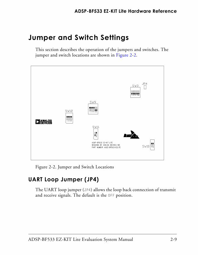
Jumper and Switch SettingsThis section describes the operation of the jumpers and switches. The jumper and switch locations are shown in Figure 2-2.
UART Loop Jumper (JP4)The UART loop jumper (JP4) allows the loop back connection of transmit and receive signals. The default is the OFF position.
Figure 2-2. Jumper and Switch Locations
Jumper and Switch Settings
2-10 ADSP-BF533 EZ-KIT Lite Evaluation System Manual
Boot Mode Switch (SW11)Positions 1 and 2 of SW11 set the boot mode of the processor as described in Table 2-4.
Test DIP Switches (SW1 and SW2)Two DIP switches (SW1 and SW2) are located on the bottom of the board. The switches are used only for testing and should be in the OFF position.
Video Configuration Switch (SW3)The video configuration switch (SW3) controls how some video signals from the ADV7183 video decoder and ADV7171 video encoder are routed to the processor’s PPI. The switch also determines if the PF2 pin controls the OE signal of the ADV7183 video decoder outputs. Table 2-5 shows which processor’s signals connect to the encoder and decoder in the default (ON) position.
Table 2-4. Boot Mode Switch (SW11)
Position 1 BMODE0 Position 2 BMODE1 Boot Mode
ON ON 16-bit external memory
OFF 1
1 Default settings
ON Flash memory
ON OFF SPI host slave
OFF OFF SPI EEPROM
Table 2-5. Video Configuration Switch (SW3)
Switch Position (Default) Processor Signal Video Signal
1 (OFF) TMR1 (HSYNC) HSYNC (ADV7171)
2 (OFF) TMR1 (HSYNC) HS (ADV7183)
ADSP-BF533 EZ-KIT Lite Evaluation System Manual 2-11
ADSP-BF533 EZ-KIT Lite Hardware Reference
Positions 1 thorough 5 of SW3 determine how and if the VSYNC, HSYNC, and FIELD control signals are routed to the processor’s PPI. In standard config-uration of the encoder and decoder, this is not necessary because the processor is capable of reading the control information embedded in the data stream.
Position 6 of SW3 determines whether PF2 connects to the OE signal of the ADV7183. When the switch is OFF, PF2 can be used for other operations, and the decoder output enable is held high with a pull-up resistor.
Push Button Enable Switch (SW9)The push button enable (SW9) switch positions 1 through 4 disconnect the drivers associated with the push buttons from the PF pins of the processor. Positions 5 and 6 are used to connect the transmit and receive frame syncs and clocks of SPORT0. This is important when the AD1836 audio codec and the processor are communicating in I2S mode. Table 2-6 shows which PF is driven when the switch is in the default (ON) position.
3 (OFF) TMR2 (VSYNC) VS (ADV7183)
4 (OFF) TMR2 (VSYNC) VSYNC (ADV7171)
5 (OFF) PF3 (FIELD) FIELD (ADV7183)
6 (ON) PF2 OE (ADV7183)
Table 2-6. Push Button Enable Switch (SW9)
Switch Position Default Setting Pin # Signal (Side 1) Pin # Signal (Side 2)
1 ON 1 SW4 12 PF8
2 ON 2 SW5 11 PF9
3 ON 3 SW6 10 PF10
Table 2-5. Video Configuration Switch (SW3) (Cont’d)
Switch Position (Default) Processor Signal Video Signal
LEDs and Push Buttons
2-12 ADSP-BF533 EZ-KIT Lite Evaluation System Manual
SPIS1/SPISS Select Switch (SW10)The SPIS1/SPISS select switch (SW10) disconnects the SPIS1 and SPISS sig-nals from the board, making them available on the SPI connector (P6). The default is the ON position.
SPORT0 Switch (SW12)When is set to OFF, SW12 disconnects SPORT0 from the audio codec. The switch is used when SPORT0 signals are desired at the expansion interface. The default is the ON position.
LEDs and Push ButtonsThis section describes the functionality of the LEDs and push buttons. Figure 2-3 shows the locations of the LEDs and push buttons.
4 ON 4 SW7 9 PF11
5 OFF 5 TFS0 8 RFS0
6 OFF 6 RSCLK0 7 TSCLK0
Table 2-6. Push Button Enable Switch (SW9) (Cont’d)
Switch Position Default Setting Pin # Signal (Side 1) Pin # Signal (Side 2)
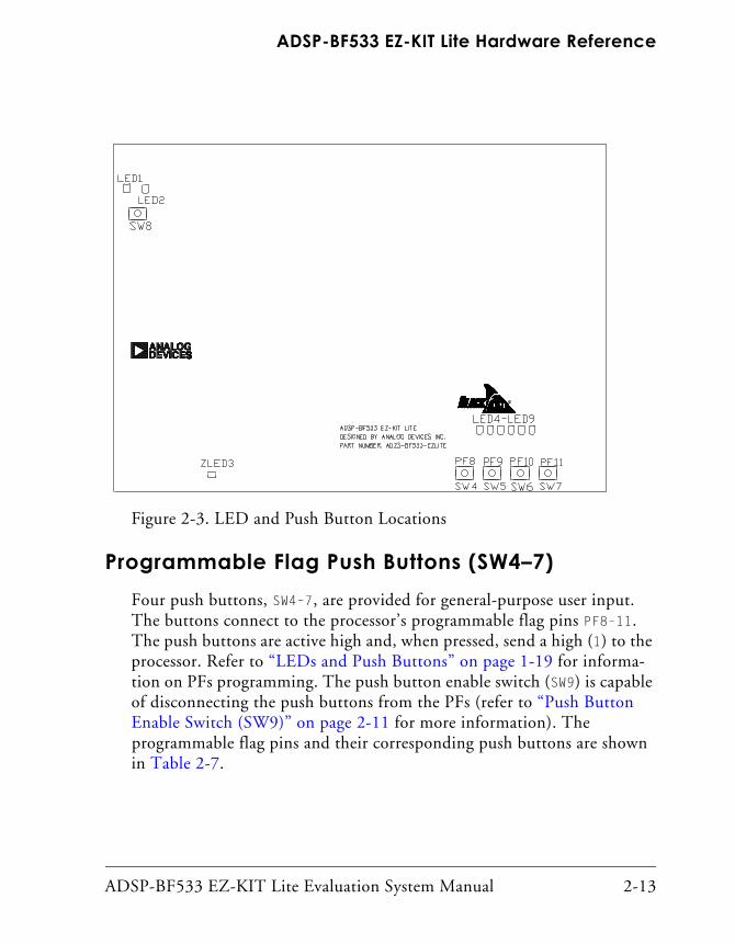
ADSP-BF533 EZ-KIT Lite Evaluation System Manual 2-13
ADSP-BF533 EZ-KIT Lite Hardware Reference
Programmable Flag Push Buttons (SW4–7)Four push buttons, SW4–7, are provided for general-purpose user input. The buttons connect to the processor’s programmable flag pins PF8–11. The push buttons are active high and, when pressed, send a high (1) to the processor. Refer to “LEDs and Push Buttons” on page 1-19 for informa-tion on PFs programming. The push button enable switch (SW9) is capable of disconnecting the push buttons from the PFs (refer to “Push Button Enable Switch (SW9)” on page 2-11 for more information). The programmable flag pins and their corresponding push buttons are shown in Table 2-7.
Figure 2-3. LED and Push Button Locations
LEDs and Push Buttons
2-14 ADSP-BF533 EZ-KIT Lite Evaluation System Manual
Reset Push Button (SW8)The RESET push button resets all of the ICs on the board. One exception is the USB interface chip (U34). The chip is not being reset when the push button is pressed after the USB cable has been plugged in, and communi-cation has been correctly initialized with the PC. After USB communication has been initialized, the only way to reset the USB is by powering down the board.
Power LED (LED1)When LED1 is lit (green), it indicates that power is being supplied to the board properly.
Reset LED (LED2)When LED2 is lit, it indicates that a master reset of all the major ICs is active.
Table 2-7. Programmable Flag Switches
Processor Programmable Flag Pin Push Button Reference Designator
PF8 SW4
PF9 SW5
PF10 SW6
PF11 SW7
ADSP-BF533 EZ-KIT Lite Evaluation System Manual 2-15
ADSP-BF533 EZ-KIT Lite Hardware Reference
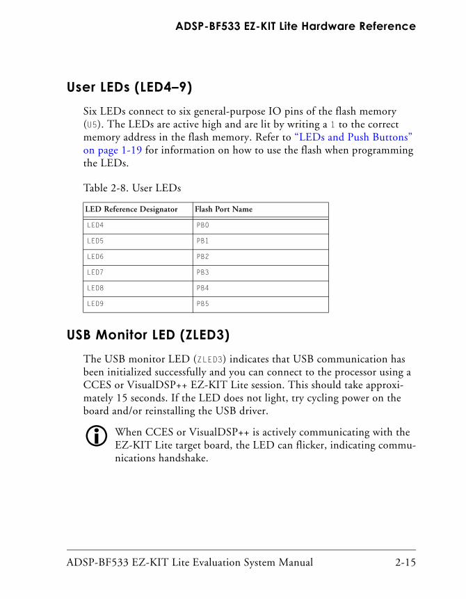
User LEDs (LED4–9)Six LEDs connect to six general-purpose IO pins of the flash memory (U5). The LEDs are active high and are lit by writing a 1 to the correct memory address in the flash memory. Refer to “LEDs and Push Buttons” on page 1-19 for information on how to use the flash when programming the LEDs.
USB Monitor LED (ZLED3)The USB monitor LED (ZLED3) indicates that USB communication has been initialized successfully and you can connect to the processor using a CCES or VisualDSP++ EZ-KIT Lite session. This should take approxi-mately 15 seconds. If the LED does not light, try cycling power on the board and/or reinstalling the USB driver.
When CCES or VisualDSP++ is actively communicating with the EZ-KIT Lite target board, the LED can flicker, indicating commu-nications handshake.
Table 2-8. User LEDs
LED Reference Designator Flash Port Name
LED4 PB0
LED5 PB1
LED6 PB2
LED7 PB3
LED8 PB4
LED9 PB5
Connectors
2-16 ADSP-BF533 EZ-KIT Lite Evaluation System Manual
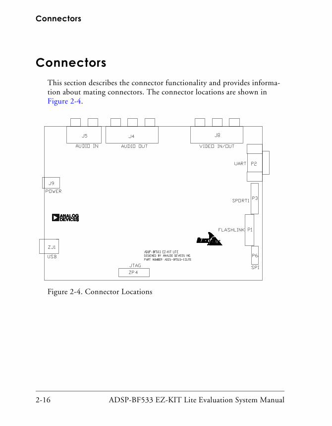
ConnectorsThis section describes the connector functionality and provides informa-tion about mating connectors. The connector locations are shown in Figure 2-4.
Figure 2-4. Connector Locations
ADSP-BF533 EZ-KIT Lite Evaluation System Manual 2-17
ADSP-BF533 EZ-KIT Lite Hardware Reference
Expansion Interface (J1–3)Three board-to-board connector footprints provide signals for most of the processor’s peripheral interfaces. The connectors are located at the bottom of the board. For more information about the expansion interface, see “Expansion Interface” on page 2-8. For availability and pricing of the J1, J2, and J3 connectors, contact Samtec.
Audio (J4 and J5)
Part Description Manufacturer Part Number
90-position 0.05” spacing,SMT (J1, J2, J3)
SAMTEC SFC-145-T2-F-D-A
Mating Connectors
90-position 0.05” spacing(through hole)
SAMTEC TFM-145-x1 series
90-position 0.05” spacing (surface mount)
SAMTEC TFM-145-x2 series
90-position 0.05” spacing (low cost)
SAMTEC TFC-145 series
Part Description Manufacturer Part Number
2x2 RCA jacks (J5) SWITCHCRAFT PJRAS2X2S01
3x2 RCA jacks (J4) SWITCHCRAFT PJRAS3X2S01
Mating Connector
Two channel RCA interconnect cable
MONSTER CABLE BI100-1M
Connectors
2-18 ADSP-BF533 EZ-KIT Lite Evaluation System Manual
Video (J8)
Power (J9)The power connector provides all of the power necessary to operate the EZ-KIT Lite board. The following table shows the power connector pinout.
The power connector supplies DC power to the EZ-KIT Lite board. Table 2-9 shows the power supply specifications.
Part Description Manufacturer Part Number
3x2 RCA jacks (J8) SWITCHCRAFT PJRAS3X2S01
Part Description Manufacturer Part Number
2.5 mm power jack (J9) SWITCHCRAFT RAPC712
DIGI-KEY RAPC712X-ND
Mating Power Supply (shipped with EZ-KIT Lite)
7.5V power supply GLOBTEK TR9CC2000LCP-Y
Table 2-9. Power Supply Specifications
Terminal Connection
Center pin +7.5 VDC@2amps
Outer ring GND
ADSP-BF533 EZ-KIT Lite Evaluation System Manual 2-19
ADSP-BF533 EZ-KIT Lite Hardware Reference
FlashLINK (P1)The FlashLINK connector allows you to configure and program the STMicroelectronics DSM2150 flash/PLD chip. See “Configuring Flash Memory” on page 1-19 for more information about the FlashLINK con-nector. The software and programming adapter to reconfigure these devices has been obsoleted and is no longer available.
RS-232 (P2)The RS-232 compatible connector is described in Table 2-10.
Part Description Manufacturer Part Number
Right-angle 7X2 shrouded 0.1” spacing (P1)
FCI 68737-414HLF
Mating Assembly
FlashLINK JTAG programmer ST MICRO FL-101B
Table 2-10. RS-232 Connector
Part Description Manufacturer Part Number
DB9, male, right angle (P2) TYCO 5747250-4
Mating Assembly
2m female-to-female cable DIGI-KEY AE1016-ND
Connectors
2-20 ADSP-BF533 EZ-KIT Lite Evaluation System Manual
SPORT1 (P3)The SPORT1 connector is linked to a 20-pin connector. The connector’s pinout can be found in “ADSP-BF533 EZ-KIT Lite Schematic” on page B-1. For the flash (U5) connector pricing and availability, contact AMP.
JTAG (ZP4)The JTAG header is the connecting point for a JTAG in-circuit emulator pod. When an emulator connects to the JTAG header, the USB debug interface is disabled.
Pin 3 is missing to provide keying. Pin 3 in the mating connector should have a plug.
When using an emulator with the EZ-KIT Lite board, follow the connection instructions provided with the emulator.
Part Description Manufacturer Part Number
20-pin IDC header FCI 68737-420HLF
Mating Connector
IDC socket DIGI-KEY S4210-ND
Part Description Manufacturer Part Number
14-pin IDC header FCI 68737-414HLF
ADSP-BF533 EZ-KIT Lite Evaluation System Manual 2-21
ADSP-BF533 EZ-KIT Lite Hardware Reference
SPI (P6)The SPI connector is linked to a 12-pin connector. The connector’s pin-out can be found in “ADSP-BF533 EZ-KIT Lite Schematic” on page B-1.
Part Description Manufacturer Part Number
IDC header FCI 68737-412HLF
Mating Assembly
IDC socket DIGI-KEY S4207-ND
Connectors
2-22 ADSP-BF533 EZ-KIT Lite Evaluation System Manual
ADSP-BF533 EZ-KIT Lite Evaluation System Manual A-1
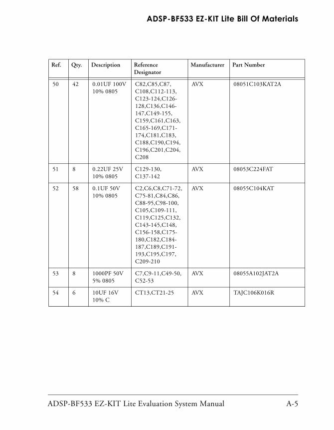
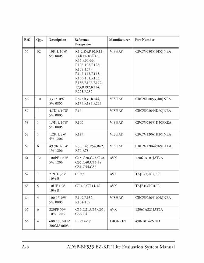
A ADSP-BF533 EZ-KIT LITE BILL OF MATERIALS
The bill of materials corresponds to “ADSP-BF533 EZ-KIT Lite Sche-matic” on page B-1.
Ref. Qty. Description Reference Designator
Manufacturer Part Number
1 2 74LVC14A SOIC14
U10,U33 TI 74LVC14AD
2 1 IDT74FCT3244APY SSOP20
U31 IDT IDT74FCT3244APYG
3 1 IDT74FCT3807AQ QSOP20
U4 IDT IDT74FCT3807AQG
4 1 SN74AHC1G00 SOT23-5
U9 TI SN74AHC1G00DBVR
5 1 12.288MHZ OSC003
U11 DIGI-KEY SG-8002CA-PCC-ND(12.288M)
6 1 SN74LVC1G125 SOT23-5
U7 TI 74LVC1G125DBVRE4
7 1 MT48LC32M16A2TG-75 TSOP54
U8 MICRON MT48LC32M16A2P-75
8 2 27MHZ OSC003
U3,U36 DIGI-KEY SG-8002CA-PCC-ND(27.00M)
9 1 32.768KHZ OSC008
U2 EPSON MC-156-32.7680KA-A0:ROHS
A-2 ADSP-BF533 EZ-KIT Lite Evaluation System Manual
10 1 IDT2305-1DC SOIC8
U46 IDT IDT2305-1DCG
11 1 SN74LVC1G32 SOT23-5
U21 TI SN74LVC1G32DBVRE4
12 1 BF533 PSD4256G6V “U5”
U5 ST MICRO PSD4256G6V-10UI
13 1 BF533 PSD4256G6V “U6”
U6 ST MICRO BF533 PSD4256G6V “U5”
14 1 FDS9431A SOIC8
U32 FAIRCHILD FDS9431A
15 1 FDC658P SOT23-6
U34 FAIRCHILD FDC658P
16 1 ADM708SARZ SOIC8
U29 ANALOG DEVICES
ADM708SARZ
17 1 ADP3338AKCZ-33 SOT-223
VR1 ANALOG DEVICES
ADP3338AKCZ-3.3-RL
18 1 ADP3339AKCZ-5 SOT-223
VR5 ANALOG DEVICES
ADP3339AKCZ-5-R7
19 1 ADP3339AKCZ-33 SOT-223
VR3 ANALOG DEVICES
ADP3339AKCZ-3.3-R7
20 2 ADP3336ARMZ MSOP8
VR2,VR6 ANALOG DEVICES
ADP3336ARMZ-REEL
21 1 ADV7171KSUZ TQFP44
U27 ANALOG DEVICES
ADV7171KSUZ
22 1 10MA AD1580BRTZ SOT23D
D1 ANALOG DEVICES
AD1580BRTZ-REEL7
Ref. Qty. Description Reference Designator
Manufacturer Part Number
ADSP-BF533 EZ-KIT Lite Evaluation System Manual A-3
ADSP-BF533 EZ-KIT Lite Bill Of Materials
23 2 ADG752BRTZ SOT23-6
U25-26 ANALOG DEVICES
ADG752BRTZ-REEL
24 3 AD8061ARTZ SOT23-5
U22-24 ANALOG DEVICES
AD8061ARTZ-R2
25 1 ADM3202ARNZ SOIC16
U30 ANALOG DEVICES
ADM3202ARNZ
26 8 AD8606ARZ SOIC8
U12-13,U15-20 ANALOG DEVICES
AD8606ARZ
27 1 AD1836AASZ MQFP52
U14 ANALOG DEVICES
AD1836AASZ
28 1 ADV7183BKSTZ LQFP80
U28 ANALOG DEVICES
ADV7183BKSTZ
29 1 ADSP-BF533-600 MINIBGA160
U1 ANALOG DEVICES
ADSP-BF533SKBCZ600
30 1 ADP1864 SOT23-6
VR4 ANALOG DEVICES
ADP1864AUJZ-R7
31 5 RUBBER FOOT
M1-5 MOUSER 517-SJ-5018BK
32 1 PWR 2.5MM_JACK CON005
J9 SWITCH-CRAFT
RAPC712X
33 1 RCA 2X2 CON013
J5 SWITCH-CRAFT
PJRAS2X2S01X
34 5 MOMEN-TARY SWT013
SW4-8 PANASONIC EVQ-PAD04M
35 3 .05 45X2 CON019
J1-3 SAMTEC SFC-145-T2-F-D-A
36 4 DIP6 SWT017
SW1-3,SW9 CTS 218-6LPST
Ref. Qty. Description Reference Designator
Manufacturer Part Number
A-4 ADSP-BF533 EZ-KIT Lite Evaluation System Manual
37 2 RCA 3X2 CON024
J4,J8 SWITCH-CRAFT
PJRAS3X2S01X
38 1 DIP4 SWT018
SW12 ITT TDA04HOSB1
39 2 DIP2 SWT020
SW10-11 C&K TDA02H0SB1
40 1 IDC 2X1 IDC2X1
JP4 FCI 90726-402HLF
41 2 IDC 7X2 IDC7X2
P1,ZP4 FCI 68737-414HLF
42 1 IDC 10X2 IDC10X2
P3 FCI 68737-420HLF
43 1 2.5A RESE-TABLE FUS001
F1 RAYCHEM SMD250F-2
44 1 IDC 2PIN_JUMPER_SHORT
SJ1 DIGI-KEY S9001-ND
45 1 DB9 9PIN DB9M
P2 TYCO 5747250-4
46 1 IDC 6X2 IDC6X2
P6 FCI 68737-412HLF
47 14 0 1/4W 5% 1206
R27-30,R148,R157-158,R167,R174-175,R177-178,R182,R193
KOA 0.0ECTRk7372BTTED
48 6 YELLOW LED001
LED4-9 PANASONIC LN1461C
49 12 330PF 50V 5% 0805
C13,C18,C23,C28,C33,C38,C67-70,C73-74
AVX 08055A331JAT
Ref. Qty. Description Reference Designator
Manufacturer Part Number
ADSP-BF533 EZ-KIT Lite Evaluation System Manual A-5
ADSP-BF533 EZ-KIT Lite Bill Of Materials
50 42 0.01UF 100V 10% 0805
C82,C85,C87,C108,C112-113,C123-124,C126-128,C136,C146-147,C149-155,C159,C161,C163,C165-169,C171-174,C181,C183,C188,C190,C194,C196,C201,C204,C208
AVX 08051C103KAT2A
51 8 0.22UF 25V 10% 0805
C129-130,C137-142
AVX 08053C224FAT
52 58 0.1UF 50V 10% 0805
C2,C6,C8,C71-72,C75-81,C84,C86,C88-95,C98-100,C105,C109-111,C119,C125,C132,C143-145,C148,C156-158,C175-180,C182,C184-187,C189,C191-193,C195,C197,C209-210
AVX 08055C104KAT
53 8 1000PF 50V 5% 0805
C7,C9-11,C49-50,C52-53
AVX 08055A102JAT2A
54 6 10UF 16V 10% C
CT13,CT21-25 AVX TAJC106K016R
Ref. Qty. Description Reference Designator
Manufacturer Part Number
A-6 ADSP-BF533 EZ-KIT Lite Evaluation System Manual
55 32 10K 1/10W 5% 0805
R1-2,R4,R10,R12-13,R15-16,R18, R26,R32-33, R106-108,R128, R138-139, R142-143,R145,R150-151,R153,R156,R166,R172-173,R192,R214,R225,R232
VISHAY CRCW080510K0JNEA
56 10 33 1/10W 5% 0805
R5-9,R31,R144,R179,R183,R224
VISHAY CRCW080533R0JNEA
57 1 4.7K 1/10W 5% 0805
R17 VISHAY CRCW08054K70JNEA
58 1 1.5K 1/10W 5% 0805
R140 VISHAY CRCW08051K50FKEA
59 1 1.2K 1/8W 5% 1206
R129 VISHAY CRCW12061K20JNEA
60 6 49.9K 1/8W 1% 1206
R38,R45,R54,R62,R70,R78
VISHAY CRCW120649K9FKEA
61 12 100PF 100V 5% 1206
C15,C20,C25,C30,C35,C40,C46-48,C51,C54,C56
AVX 12061A101JAT2A
62 1 2.2UF 35V 10% B
CT27 AVX TAJB225K035R
63 5 10UF 16V 10% B
CT1-2,CT14-16 AVX TAJB106K016R
64 4 100 1/10W 5% 0805
R149,R152,R154-155
VISHAY CRCW0805100RJNEA
65 6 220PF 50V 10% 1206
C16,C21,C26,C31,C36,C41
AVX 12061A221JAT2A
66 4 600 100MHZ 200MA 0603
FER14-17 DIGI-KEY 490-1014-2-ND
Ref. Qty. Description Reference Designator
Manufacturer Part Number
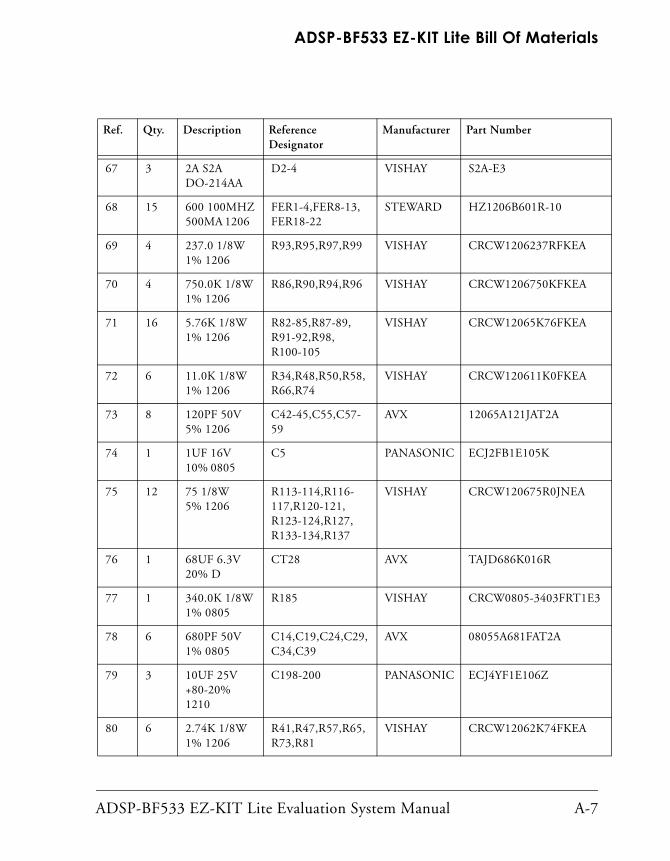
ADSP-BF533 EZ-KIT Lite Evaluation System Manual A-7
ADSP-BF533 EZ-KIT Lite Bill Of Materials
67 3 2A S2A DO-214AA
D2-4 VISHAY S2A-E3
68 15 600 100MHZ 500MA 1206
FER1-4,FER8-13,FER18-22
STEWARD HZ1206B601R-10
69 4 237.0 1/8W 1% 1206
R93,R95,R97,R99 VISHAY CRCW1206237RFKEA
70 4 750.0K 1/8W 1% 1206
R86,R90,R94,R96 VISHAY CRCW1206750KFKEA
71 16 5.76K 1/8W 1% 1206
R82-85,R87-89,R91-92,R98,R100-105
VISHAY CRCW12065K76FKEA
72 6 11.0K 1/8W 1% 1206
R34,R48,R50,R58,R66,R74
VISHAY CRCW120611K0FKEA
73 8 120PF 50V 5% 1206
C42-45,C55,C57- 59
AVX 12065A121JAT2A
74 1 1UF 16V 10% 0805
C5 PANASONIC ECJ2FB1E105K
75 12 75 1/8W 5% 1206
R113-114,R116-117,R120-121,R123-124,R127,R133-134,R137
VISHAY CRCW120675R0JNEA
76 1 68UF 6.3V 20% D
CT28 AVX TAJD686K016R
77 1 340.0K 1/8W 1% 0805
R185 VISHAY CRCW0805-3403FRT1E3
78 6 680PF 50V 1% 0805
C14,C19,C24,C29,C34,C39
AVX 08055A681FAT2A
79 3 10UF 25V +80-20% 1210
C198-200 PANASONIC ECJ4YF1E106Z
80 6 2.74K 1/8W 1% 1206
R41,R47,R57,R65,R73,R81
VISHAY CRCW12062K74FKEA
Ref. Qty. Description Reference Designator
Manufacturer Part Number
A-8 ADSP-BF533 EZ-KIT Lite Evaluation System Manual
81 12 5.49K 1/8W 1% 1206
R35,R40,R42,R49,R51,R56,R59,R64,R67,R72,R75,R80
VISHAY CRCW12065K49FKEA
82 6 3.32K 1/8W 1% 1206
R36,R43,R52,R60,R68,R76
VISHAY CRCW12063K32FKEA
83 6 1.65K 1/8W 1% 1206
R37,R44,R53,R61,R69,R77
VISHAY CRCW12061K65FKEA
84 10 10UF 16V 20% CAP002
CT3-12 PANASONIC EEE1CA100SR
85 1 4A SSB43L DO-214AA
D6 VISHAY SSB43L
86 1 10UH 20% IND001
L12 TDK 445-2014-1-ND
87 2 10K 50MW 5% BGA36
RN1-2 CTS RT230B7TR7
88 25 0 1/10W 5% 0805
R3,R19,R21-25,R110-111,R132,R135-136,R141,R169,R186-188,R194,R210-211,R222,R226-228,R231
VISHAY CRCW08050000Z0EA
89 1 190 100MHZ 5A FER002
FER23 MURATA DLW5BSN191SQ2
90 1 3.32K 1/10W 1% 0805
R223 PANASONIC ERJ-6ENF3321V
91 4 22 1/10W 5% 0805
R14,R109,R180- 181
VISHAY CRCW080522R0JNEA
92 6 0.68UH 10% 0805
L4-9 MURATA LQM21NNR68K10D
93 1 .082UF 50V 5% 0805
C83 AVX 08055C823JAT2A
Ref. Qty. Description Reference Designator
Manufacturer Part Number

ADSP-BF533 EZ-KIT Lite Evaluation System Manual A-9
ADSP-BF533 EZ-KIT Lite Bill Of Materials
94 1 1A ZHCS1000 SOT23-312
D5 ZETEX ZHCS1000TA pb-free
95 3 2.2UH 10% 0805
L1-3 DIGI-KEY 490-1119-2-ND
96 6 1UF 10V 10% 0805
C4,C60-61,C102-104
AVX 0805ZC105KAT2A
97 2 18PF 50V 5% 0805
C1,C3 AVX 08055A180JAT2A
98 1 10M 1/8W 5% 0805
R20 VISHAY CRCW080510M0JMEA
99 1 64.9K 1/10W 1% 0805
R184 VISHAY CRCW080564K9FKEA
100 1 76.8K 1/10W 1% 1206
R190 VISHAY CRCW120676K8FKEA
101 1 147.0K 1/10W 1% 1206
R191 VISHAY CRCW1206147KFKEA
102 1 68PF 50V 5% 0603
C64 AVX 06035A680JAT2A
103 1 470PF 50V 5% 0603
C63 AVX 06033A471JAT2A
104 1 0 1/10W 5% 0603
R159 PHYCOMP 232270296001L
105 1 24.9K 1/10W 1% 0603
R11 DIGI-KEY 311-24.9KHTR-ND
106 1 47UF 6.3V 10% B
CT26 PANASONIC EEE0JA470WR
107 1 0.05 1/2W 1% 1206
R165 SUSUMU PRL1632-R051-F-T1
108 1 10UF 16V 10% 1210
C65 AVX 1210YD106KAT2A
Ref. Qty. Description Reference Designator
Manufacturer Part Number
A-10 ADSP-BF533 EZ-KIT Lite Evaluation System Manual
109 1 680 1/8W 5% 1206
R163 VISHAY CRCW1206680RFNEA
110 1 150.0 1/8W 1% 1206
R122 VISHAY CRCW1206150RFKEA
111 1 GREEN LED001
LED1 PANASONIC LN1361CTR
112 1 RED LED001 LED2 PANASONIC LN1261CTR
113 2 1000PF 50V 5% 1206
C96-97 AVX 12065A102JAT2A
114 6 2200PF 50V 5% 1206
C12,C17,C22,C27,C32,C37
AVX 12065A222JAT050
115 6 1K 1/8W 5% 1206
R115,R118-119,R125-126,R131
VISHAY CRCW12061K00FNEA
116 3 100K 1/8W 5% 1206
R112,R130,R176 VISHAY CRCW1206100KFKEA
117 7 270 1/8W 5% 1206
R146-147,R160-162,R164,R168
VISHAY CRCW1206270RJNEA
118 6 604.0 1/8W 1% 1206
R39,R46,R55,R63,R71,R79
PANASONIC ERJ-8ENF6040V
119 4 1UF 25V 20% A
CT17-20 AVX TAJA105K020R
120 1 255.0K 1/10W 1% 0603
R171 VISHAY CRCW06032553FK
121 1 80.6K 1/10W 1% 0603
R170 DIGI-KEY 311-80.6KHRCT-ND
122 1 6.8UH 25% IND009
L10 DIGI-KEY 308-1328-1-ND
Ref. Qty. Description Reference Designator
Manufacturer Part Number

D
4
3
2
1
A B C
20 Cotton Road
Nashua, NH 03063
A B C D
4
3
2
1
PH: 1-800-ANALOGD
C
Title
Size Board No.
Date Sheet of
DEVICESANALOG
Rev
ADSP-BF533 EZ-KIT LITE
A0167-2001 2.2
ADSP-BF533 EZ-KIT Lite
1 125-24-2007_14:20
TITLE
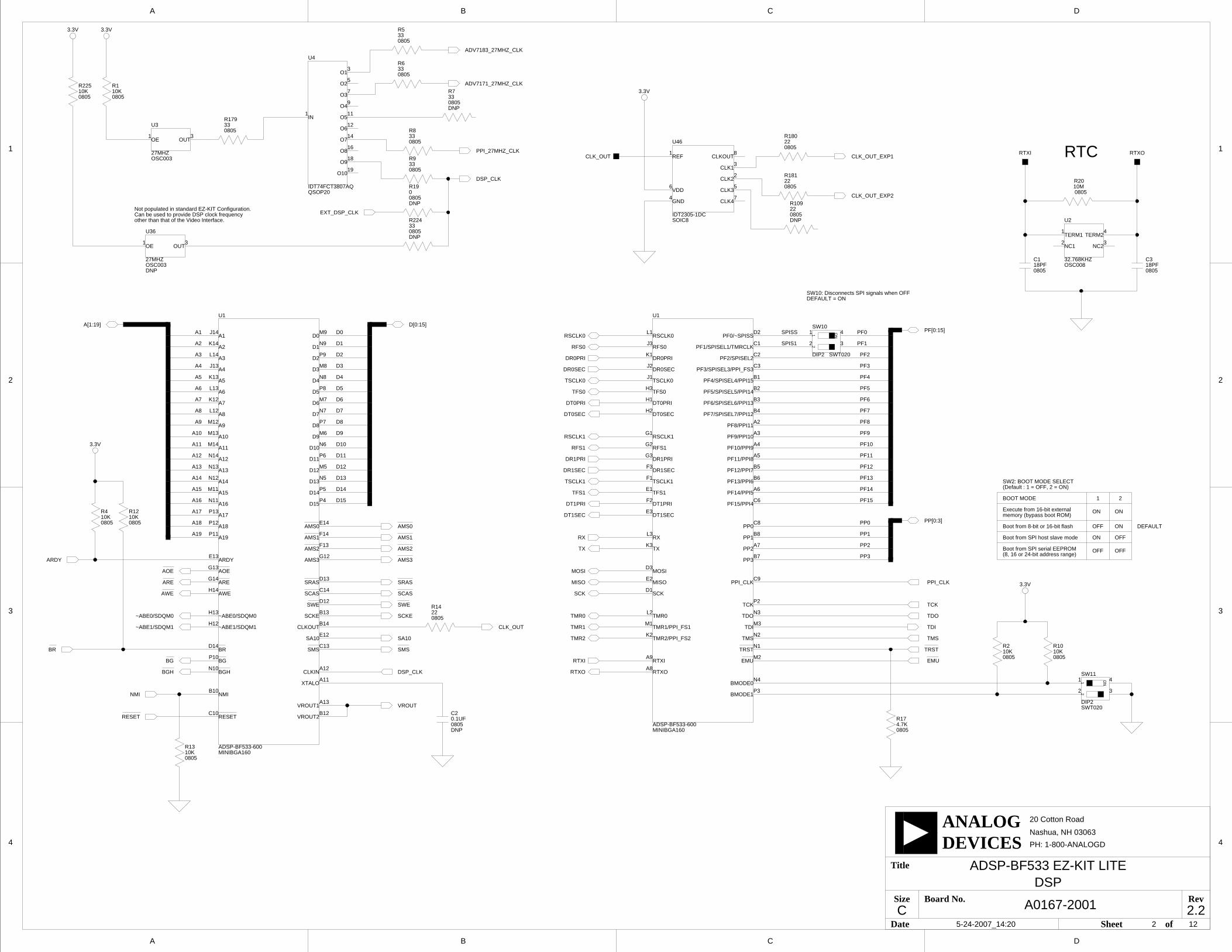
3.3V
3.3V
3.3V
3.3V
IN
O1
O10
O2
O3
O4
O5
O6
O7
O8
O9
NC1 NC2
TERM1 TERM2
D
4
3
2
1
A B C
20 Cotton Road
Nashua, NH 03063
A B C D
4
3
2
1
PH: 1-800-ANALOGD
C
Title
Size Board No.
Date Sheet of
DEVICESANALOG
Rev
ADSP-BF533 EZ-KIT LITE
A0167-2001 2.2
OE OUT
CLK2
CLK1
GND
CLK3VDD
CLK4
CLKOUTREF
OE OUT
3.3V
12
ON
12
ON
BMODE0
BMODE1
DR0PRI
DR0SEC
DR1PRI
DR1SEC
DT0PRI
DT0SEC
DT1PRI
DT1SEC
PP0
PP1
PP2
PP3
PPI_CLK
RFS0
RFS1
RSCLK0
RSCLK1
RTXI
RTXO
RX
SCK
TCK
TDI
TDO
TFS0
TFS1
TMR0
TMR1/PPI_FS1
TMR2/PPI_FS2 TMS
TSCLK0
TSCLK1
TX
EMU
TRST
MOSI
MISO
PF0/~SPISS
PF1/SPISEL1/TMRCLK
PF2/SPISEL2
PF3/SPISEL3/PPI_FS3
PF4/SPISEL4/PPI15
PF5/SPISEL5/PPI14
PF6/SPISEL6/PPI13
PF7/SPISEL7/PPI12
PF8/PPI11
PF9/PPI10
PF10/PPI9
PF11/PPI8
PF12/PPI7
PF13/PPI6
PF14/PPI5
PF15/PPI4
A1
A10
A11
A12
A13
A14
A15
A16
A17
A18
A19
A2
A3
A4
A5
A6
A7
A8
A9
AMS3ARDY
CLKIN
CLKOUT
D0
D1
D10
D11
D12
D13
D14
D15
D2
D3
D4
D5
D6
D7
D8
D9
NMI
SA10
SCKE
VROUT1
VROUT2
XTALO
~ABE0/SDQM0
~ABE1/SDQM1
AMS0
AMS1
AMS2
AOE
ARE
AWE
BG
BGH
BR
RESET
SCAS
SMS
SRAS
SWE
OFF
ON
RTC
other than that of the Video Interface.
Not populated in standard EZ-KIT Configuration.
memory (bypass boot ROM)
Boot from 8-bit or 16-bit flash
Boot from SPI host slave mode
(8, 16 or 24-bit address range)
Execute from 16-bit external
SW2: BOOT MODE SELECT(Default : 1 = OFF, 2 = ON)
ON ON
ON
OFF
OFF
OFFBoot from SPI serial EEPROM
21BOOT MODE
DEFAULT
Can be used to provide DSP clock frequency
SW10: Disconnects SPI signals when OFFDEFAULT = ON
J14
M13
M14
N14
N13
N12
M11
N11
P13
P12
P11
K14
L14
J13
K13
L13
K12
L12
M12
G12E13
A12
B14
M9
N9
N6
P6
M5
N5
P5
P4
P9
M8
N8
P8
M7
N7
P7
M6
B10
E12
B13
A13
B12
A11
H13
H12
E14
F14
F13
G13
G14
H14
P10
N10
D14
C10
C14
C13
D13
D12
ADSP-BF533-600MINIBGA160
U1
N4
P3
K1
J2
G3
F3
H1
H2
F2
E3
C8
B8
A7
B7
C9
J3
G2
L1
G1
A9
A8
L3
D1
P2
M3
N3
H3
E1
L2
M1
K2 N2
J1
F1
K3
M2
N1
D3
E2
D2
C1
C2
C3
B1
B2
B3
B4
A2
A3
A4
A5
B5
B6
A6
C6
U1
MINIBGA160ADSP-BF533-600
1
2
4
3
SW10
DIP2 SWT020
1
2
4
3
SW11
DIP2SWT020
10K0805
R10
SCK
TMS
TDI
TRST
EMU
TDO
TCK
R2010M0805
C2
08050.1UF
DNP
1 3
U3
OSC00327MHZ
2
3
4
56
7
81
SOIC8
U46
IDT2305-1DC
R1900805DNP
R7330805DNP
R224330805DNP
R109220805DNP
1 3
DNP
U36
OSC00327MHZ
DSP_CLK
R22510K0805
EXT_DSP_CLK
080533R179
R2
080510K
2 125-24-2007_14:20
DSP
2
1
3
4
U2
OSC00832.768KHZ
1
3
19
5
7
9
11
12
14
16
18
U4
QSOP20IDT74FCT3807AQ
R180220805
CLK_OUT_EXP1
CLK_OUT_EXP2
080522R181
CLK_OUT
CLK_OUT
080522R14
080533R8
C3
080518PF
C1
080518PF
R5330805
PPI_27MHZ_CLK
ADV7183_27MHZ_CLK
ADV7171_27MHZ_CLK
D0
D1
D2
D3
D4
D5
D6
D7
D8
D9
D10
D11
D12
D13
D14
D[0:15]
D15
A11
A10
A8
A9
A12
A4
A1
A19
A17
A15
A[1:19]
A5
A2
A3
A6
A7
A13
A14
A16
A18
BG
NMI
RESET
VROUT
DSP_CLK
4.7K0805
R17
PPI_CLK
TSCLK1
RSCLK1
TSCLK0
RSCLK0
R4
080510K
R9330805
DR1SEC
PP[0:3]
PP3
PP2
PP1
PP010K0805
R12
080533R6
080510KR1
RTXO
RTXI
TMR0
TMR1
TMR2
MOSI
MISO
TX
RX
RFS1
DR1PRI
TFS1
DT1PRI
DT1SEC
RFS0
DR0PRI
TFS0
DT0PRI
DT0SEC
DR0SEC
10K0805
R13
AMS0
AMS1
AMS2
AMS3
BGH
~ABE1/SDQM1
~ABE0/SDQM0
AWE
ARE
AOE
SRAS
SCAS
SWE
SCKE
SA10
SMS
RTXI RTXO
BR
ARDY
SPIS1
SPISS
PF2
PF3
PF4
PF5
PF6
PF7
PF8
PF9
PF10
PF11
PF12
PF13
PF14
PF15
PF1
PF0 PF[0:15]
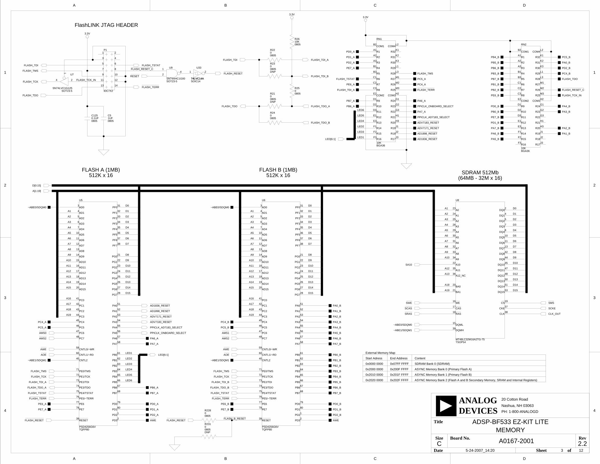
3.3V
D
4
3
2
1
A B C
20 Cotton Road
Nashua, NH 03063
A B C D
4
3
2
1
PH: 1-800-ANALOGD
C
Title
Size Board No.
Date Sheet of
DEVICESANALOG
Rev
ADSP-BF533 EZ-KIT LITE
A0167-2001 2.2
3.3V
COM2
R16
R15
R14
R13
R12
R10
R24
R23
R22
R21
R20
R19
R27
R28
R29
R30
R31
R32
R2
R3
R4
R5
R6
R7
R8
R26
R1
R18
COM1
R9
R11
COM4
R25
COM3
R17
3.3V
COM2
R16
R15
R14
R13
R12
R10
R24
R23
R22
R21
R20
R19
R27
R28
R29
R30
R31
R32
R2
R3
R4
R5
R6
R7
R8
R26
R1
R18
COM1
R9
R11
COM4
R25
COM3
R17
PE7
PE3/TDO
PE2/TDI
PE1/TCK
PE0/TMS
PB7
PB6
PB5
PB4
PB3
PB2
PB1
PB0CNTL1/~RD
CNTL0/~WR
PA7
PA6
PA5
PA4
PA3
PA2
PA1
PA0
PC7
PC6
PC5
PC4
PC3
PC0
CNTL2
PF7
PF6
PF4
PF5
PF3
PF2
PF1
PG7
PG6
PG5
PG4
PG3
PG2
PG1
PG0
AD15
AD14
AD13
AD12
AD11
AD10
AD9
AD8
AD7
AD6
AD5
AD4
AD3
AD2
AD1
AD0
PD3
PF0
PD1
PC2
PC1
RESET
PD2
PD0PE6
PE5/~TERR
PE4/TSTAT
A0
A1
A10
A11
A12_NC
A2
A3
A4
A5
A6
A7
A8
A9
CKE
CLK
DQ0
DQ1
DQ10
DQ11
DQ12
DQ13
DQ14
DQ15
DQ2
DQ3
DQ4
DQ5
DQ6
DQ7
DQ8
DQ9
DQMH
DQML
CAS
CS
RAS
WE
BA1
BA0
Content
512K x 16512K x 16FLASH A (1MB)
FlashLINK JTAG HEADER
SDRAM 512Mb(64MB - 32M x 16)
Start Adress
0x0000 0000
0x2000 0000
0x2010 0000
0x2020 0000
0x07FF FFFF
0x200F FFFF
0x201F FFFF
0x202F FFFF
External Memory Map
End Address
SDRAM Bank 0 (SDRAM)
ASYNC Memory Bank 0 (Primary Flash A)
ASYNC Memory Bank 1 (Primary Flash B)
ASYNC Memory Bank 2 (Flash A and B Secondary Memory, SRAM and Internal Registers)
FLASH B (1MB)
23
24
22
35
36
25
26
29
30
31
32
33
34
37
38
2
4
45
47
48
50
51
53
5
7
8
10
11
13
42
44
39
15
17
19
18
16
21
20
U8
MT48LC32M16A2TG-75TSOP54
78
74
73
72
71
68
67
66
65
64
63
62
6160
59
58
57
56
55
54
53
52
51
48
47
46
45
44
41
40
38
37
35
36
34
33
32
28
27
26
25
24
23
22
21
20
19
18
17
16
15
14
13
12
11
10
7
6
5
4
3
2
31
80
43
42
39
1
7977
76
75
U6
TQFP80PSD4256G6V
78
74
73
72
71
68
67
66
65
64
63
62
6160
59
58
57
56
55
54
53
52
51
48
47
46
45
44
41
40
38
37
35
36
34
33
32
28
27
26
25
24
23
22
21
20
19
18
17
16
15
14
13
12
11
10
7
6
5
4
3
2
31
80
43
42
39
1
7977
76
75
U5
PSD4256G6VTQFP80
E2
F3
F2
F1
E3
E1
D2
G1
G2
G3
H1
H3
J1
M1
L3
L1
K3
K2
K1
A2
A3
B1
B3
C1
C2
C3
M2
A1
J2
B2
D1
D3
L2
M3
H2
J3
BGA3610K
RN1
1
24
U9
SN74AHC1G00SOT23-5
1
3
5
7
9
11
13
2
4
6
8
10
12
14
IDC7X2
P1
24
1
SOT23-5
U7
SN74LVC1G125
1 2
74LVC14ASOIC14
U33
74LVC14A
FLASH_RESET_C
08050R21
DNP
08050R23
DNP
08050R231
DNP
R22800805
~ABE0/SDQM0
~ABE1/SDQM1
~ABE0/SDQM0
SRAS
SCAS
SWE
CLK_OUT
1UF0805
C5
SMS
SCKE
SA10
PA7_A
PA6_A
PPICLK_ONBOARD_SELECT
PPICLK_AD7183_SELECT
ADV7183_RESET
ADV7171_RESET
AD1898_RESET
AD1836_RESET
LED5
LED4
LED3
LED2
LED6
LED[6:1]LED1
PB7_A
PB6_A
J3
H2
M3
L2
D3
D1
B2
J2
A1
M2
C3
C2
C1
B3
B1
A3
A2
K1
K2
K3
L1
L3
M1
J1
H3
H1
G3
G2
G1
D2
E1
E3
F1
F2
F3
E2
BGA3610K
RN2
08050R22
08050R25
08050R24
080510KR26
PE6_A
PE7_A
FLASH_TMS
FLASH_TCK
FLASH_TDI_A
PD0_A
PD1_A
PD2_A
AWE
PC4_A
PC5_A
AMS0
3 125-24-2007_14:20
MEMORY
~ABE1/SDQM1
FLASH_RESET
FLASH_TERR
FLASH_TSTAT
FLASH_TDO_A
AOE
AWE
AMS2
0.1UF0805
C125
FLASH_RESET
PA1_B
FLASH_TSTAT
LED6
LED[6:1]LED1
LED3
LED4
LED5
LED2
FLASH_TCK_IN
FLASH_RESET_C
FLASH_TDO
PA5_B
PA6_B
PA7_B
PD1_B
PE7_B
PD0_B
PE6_B
FLASH_TERR
FLASH_TMS
ADV7171_RESET
ADV7183_RESET
PE6_A
PE7_A
PD2_A
PD1_A
PD0_A
FLASH_TDI_A
PB7_A
PB6_A
PA6_A
PPICLK_ONBOARD_SELECT
PA7_A
PPICLK_AD7183_SELECT
AD1898_RESET
AD1836_RESET
PC5_A
PC4_A
PB4_B
PB5_B
PB6_B
PB3_B
PB7_B
PB2_B
PB1_B
PB0_B
PA4_B
PA3_B
PA2_B
PC5_B
PD2_B
PA0_B
PC4_BFLASH_TDI_B
FLASH_TCK
FLASH_TDO_B
FLASH_TDI_A
FLASH_TDO
FLASH_TDI
FLASH_TDO
FLASH_TCK_IN
FLASH_TERR
FLASH_TSTATFLASH_TDI
FLASH_TDO_A
FLASH_TMSFLASH_RESET
RESET
PE7_B
PB7_B
PB6_B
PB5_B
PB4_B
PB3_B
PB2_B
PB1_B
PB0_B
PA7_B
PA6_B
PA5_B
PA4_B
PA3_B
PA2_B
PA1_B
PA0_B
PC5_B
PC4_B
~ABE1/SDQM1
~ABE0/SDQM0
AWE
PD1_B
PD2_B
PD0_BPE6_B
FLASH_B_RESET
FLASH_TERR
FLASH_TSTAT
D12
D11
D10
D9
D8
D7
D6
D5
D4
D2
D1
D0
D3
D14
D13
D15
D0
D1
D2
D4
D6
D11
D12
D13
D14
D15
D8
D7
D0
D1
D2
D3
D4
D5
D6
D9
D10
D11
D12
D13
D14
D15
D[0:15]
D8
D9
D7
D3
D5
D10
FLASH_TDO_B
FLASH_TDI_B
FLASH_TCK
FLASH_TMS
AOE
AWE
AMS2
AMS1
A13
A12
A9
A8
A7
A6
A5
A4
A3
A2
A1
A10
A19
A18
A1
A[1:19]
A3
A4
A5
A6
A7
A8
A9
A10
A11
A12
A13
A14
A17
A18
A19
A16
A15
A2
A19
A18
A17
A16
A15
A14
A13
A12
A11
A10
A8
A7
A6
A4
A3
A2
A1
A9
A5
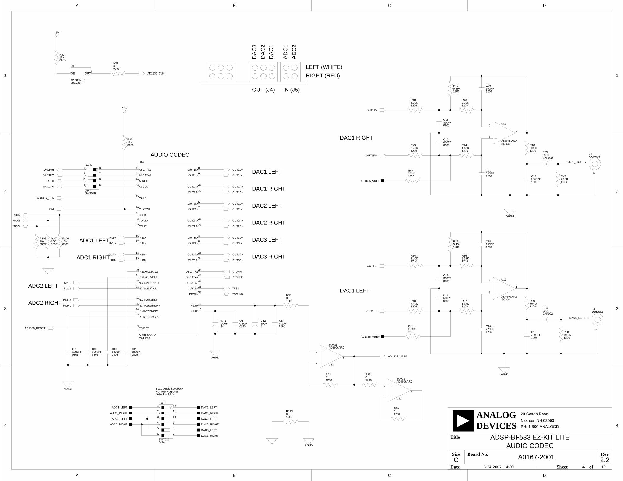
AGND
AGND
AGND
3.3V
D
4
3
2
1
A B C
20 Cotton Road
Nashua, NH 03063
A B C D
4
3
2
1
PH: 1-800-ANALOGD
C
Title
Size Board No.
Date Sheet of
DEVICESANALOG
Rev
ADSP-BF533 EZ-KIT LITE
A0167-2001 2.2
OE OUT
3.3V
12
45
6
ON
3
AGND
PD/RST
IN2R+/CR2/CR2
IN2R-/CR1/CR1
NC/IN2R1/IN2R+
NC/IN2R2/IN2R-
NC/IN2L2/IN2L-
NC/IN2L1/IN2L+
IN2L-/CL1/CL1
IN2L+/CL2/CL2
FILTD
FILTR
OUT3R-
OUT3R+
OUT3L-
OUT3L+
OUT2R-
OUT2R+
OUT2L-
OUT2L+
OUT1R-
OUT1R+
OUT1L-
OUT1L+
IN1R-
IN1R+
IN1L-
IN1L+
COUT
CDATA
CCLK
CLATCH
MCLK
DLRCLK
DBCLK
ASDATA1
ASDATA2
ALRCLK
ABCLK
DSDATA2
DSDATA1
DSDATA3
ON1
23
4
AGND
For Test PurposesDefault = All Off
DAC1 LEFT
DAC1 LEFT
DAC1 RIGHT
DAC2 LEFT
DAC2 RIGHT
DAC3 LEFT
DAC3 RIGHT
ADC2 LEFT
ADC2 RIGHT
ADC1 LEFT
ADC1 RIGHT
DAC1 RIGHT
DA
C1
DA
C2
DA
C3
AD
C1
AD
C2
OUT (J4)
RIGHT (RED)
LEFT (WHITE)
IN (J5)
AUDIO CODEC
SW1: Audio Loopback
2
3
1
4 5
6
7
8SW12
DIP4SWT018
RSCLK0
RFS0
3
27
26
25
24
23
22
21
20
12
13
34
35
5
4
32
33
7
6
30
31
9
8
19
18
17
16
49
2
51
50
45
38
41
42
36
37
47
48
44
43
MQFP52
U14
AD1836AASZ
6
5
7
SOIC8
U12
AD8606ARZ
1
3
2
SOIC8
U12
AD8606ARZ
PF4
DR0PRI
8
9
J4CON024
9
7
J4CON024
1
2
3
4
5
6 7
8
9
10
11
12SW1
DIP6SWT017
ADC1_LEFT
DAC3_RIGHT
DAC3_LEFT
DAC2_RIGHT
DAC2_LEFT
DAC1_RIGHT
DAC1_LEFT
10K0805
R33
TFS0
TSCLK0
R29
12060
12060R28
01206
R27
1
3
2
SOIC8
U13
AD8606ARZR3001206
DAC1_LEFT
CAP00210UFCT4
49.9K1206
R45
DAC1_RIGHT
CAP00210UFCT3
OUT3R+
DT0PRI
DT0SEC
OUT3R-
OUT3L-
OUT2R-
OUT2L-
OUT1L-
OUT1R+
OUT1R-
AD1836_VREF
12062.74KR41
1 3
12.288MHZOSC003
U11
SCK
08051000PFC7
0.1UF0805
C810UFB
CT2
08050.1UFC6
B10UFCT1
330805
R31
AD1836_CLK
4 125-24-2007_14:20
AUDIO CODEC
080510KR32
1000PF0805
C9
08051000PFC10
1000PF0805
C11
AD1836_RESET
IN2R1
IN2R2
IN2L2
IN2L1
OUT1L+
OUT1L-
OUT1R+
OUT1R-
OUT2L+
OUT2R+
OUT3L+
IN1R-
IN1R+
IN1L-
IN1L+
MISO
MOSI
7
5
6
SOIC8
U13
AD8606ARZ
5.49K1206
R49
11.0K1206
R48
12062.74KR47
1206604.0R46
220PF1206
C21
1.65K1206
R44
100PF1206
C20
3.32K1206
R43
5.49K1206
R42
680PF0805
C19
330PF0805
C18
2200PF1206
C17
5.49K1206
R40
1206604.0R39
220PF1206
C16
1.65K1206
R37
100PF1206
C15
3.32K1206
R36
5.49K1206
R35
680PF0805
C14
330PF0805
C13
11.0K1206
R34
2200PF1206
C12
OUT1L+
AD1836_VREF
AD1836_VREF49.9K1206
R38
01206
R193
R106
080510K10K
0805
R107R108
080510K
DR0SEC
ADC2_RIGHT
ADC2_LEFT
ADC1_RIGHT
AD1836_CLK

AGND
AGND
AGND
D
4
3
2
1
A B C
20 Cotton Road
Nashua, NH 03063
A B C D
4
3
2
1
PH: 1-800-ANALOGD
C
Title
Size Board No.
Date Sheet of
DEVICESANALOG
Rev
ADSP-BF533 EZ-KIT LITE
A0167-2001 2.2
AGND
DAC2 RIGHT
DAC3 RIGHT
DAC3 LEFTDAC2 LEFT
CAP00210UFCT5
CAP00210UFCT6
CAP00210UFCT7
CAP00210UFCT8
100PF1206
C25
1206604.0R63
1206604.0R55
5
6
J4CON024
4
6
J4CON024
3
1
J4CON024
2
3
J4CON024
5 125-24-2007_14:20
AUDIO OUT
1
3
2
SOIC8
U15
AD8606ARZ
49.9K1206
R62
DAC3_RIGHT
DAC3_LEFT
49.9K1206
R54
49.9K1206
R78
DAC2_LEFT
49.9K1206
R70
DAC2_RIGHT
OUT3R-
OUT3R+
2200PF1206
C27
7
5
6
SOIC8
U15
AD8606ARZ
5.49K1206
R64
11.0K1206
R58
2200PF1206
C22
1.65K1206
R53
220PF1206
C26
3.32K1206
R52
5.49K1206
R51
11.0K1206
R50
5.49K1206
R56
12062.74KR65
220PF1206
C31
1.65K1206
R61
100PF1206
C30
3.32K1206
R60
5.49K1206
R59
680PF0805
C29
330PF0805
C28
12062.74KR57
680PF0805
C24
330PF0805
C23
AD1836_VREF
AD1836_VREF
OUT3L-
OUT3L+
7
5
6
SOIC8
U16
AD8606ARZ
12062.74KR81
5.49K1206
R80
1206604.0R79
220PF1206
C41
1.65K1206
R77
100PF1206
C40
3.32K1206
R76
5.49K1206
R75
680PF0805
C39
330PF0805
C38
11.0K1206
R74
2200PF1206
C37
1
3
2
SOIC8
U16
AD8606ARZ
12062.74KR73
5.49K1206
R72
1206604.0R71
220PF1206
C36
1.65K1206
R69
100PF1206
C35
3.32K1206
R68
5.49K1206
R67
680PF0805
C34
330PF0805
C33
11.0K1206
R66
2200PF1206
C32
AD1836_VREF
OUT2L+
OUT2L-
OUT2R+
OUT2R-
AD1836_VREF
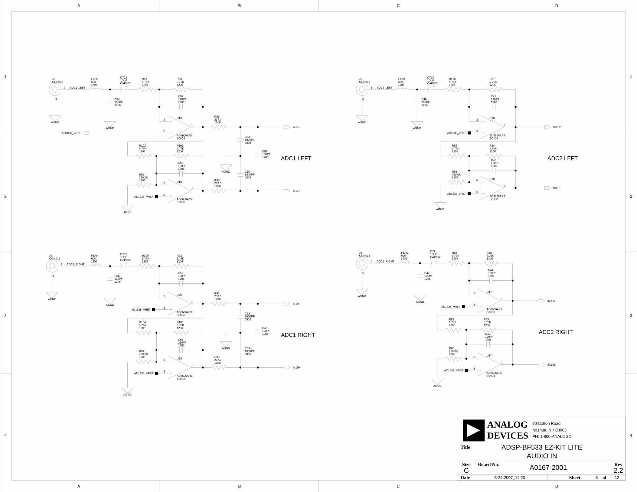
AGND
AGND
AGND
AGND
AGND
AGND
AGND
AGND
AGND
AGND
D
4
3
2
1
A B C
20 Cotton Road
Nashua, NH 03063
A B C D
4
3
2
1
PH: 1-800-ANALOGD
C
Title
Size Board No.
Date Sheet of
DEVICESANALOG
Rev
ADSP-BF533 EZ-KIT LITE
A0167-2001 2.2
AGND
AGND
AGND
AGND
ADC1 RIGHT
ADC1 LEFT
ADC2 RIGHT
ADC2 LEFT
C46100PF1206
1206100PFC47
100PFC56
1206
C54100PF1206
5
6
J5CON013
3
1
J5CON013
2
3
J5CON013
6
4
J5CON013
1206
FER2600
237.0R93
1206
7
5
6 U18
SOIC8AD8606ARZ
6
5
7
U17
SOIC8AD8606ARZ
2
3
1
U17
SOIC8AD8606ARZ
2
3
1
U20
SOIC8AD8606ARZ
5.76KR89
1206
100PFC48
1206
C531000PF0805
C501000PF0805
C51100PF1206
1000PFC49
0805
1000PFC52
0805
1
3
2 U18
SOIC8AD8606ARZ
6
5
7
U20
SOIC8AD8606ARZ
IN2R2
IN2R1
750.0KR90
1206
1206
C42120PF
5.76KR83
12065.76KR82
1206
120PFC44
1206
5.76KR88
1206CAP00210UFCT9
ADC2_RIGHT
IN1R-
237.0R95
1206
120PFC59
1206
R925.76K1206
R1005.76K1206
10UFCT11
CAP002
ADC1_RIGHT
FER4
1206600
750.0KR94
1206
R1045.76K1206
R1035.76K1206
1206
C55120PF
IN1R+
ADC1_LEFT
IN1L+
IN1L-
7
5
6 U19
SOIC8AD8606ARZ
1
3
2 U19
SOIC8AD8606ARZ
FER3
1206600
IN2L1
IN2L2
ADC2_LEFT
AD1836_VREF
6 125-24-2007_14:20
AUDIO IN
R1055.76K1206
CT1210UFCAP002
R1025.76K1206
1206120PFC58
R1015.76K1206
C57120PF1206
R99237.01206
R985.76K1206
R97237.01206
R96750.0K1206
12065.76KR91 R87
5.76K1206
R86750.0K1206
FER1
1206600
C45120PF1206
R855.76K1206
R845.76K1206
1206120PFC43
CT1010UFCAP002
AD1836_VREF
AD1836_VREFAD1836_VREF
AD1836_VREF
AD1836_VREF
AD1836_VREF
AD1836_VREF
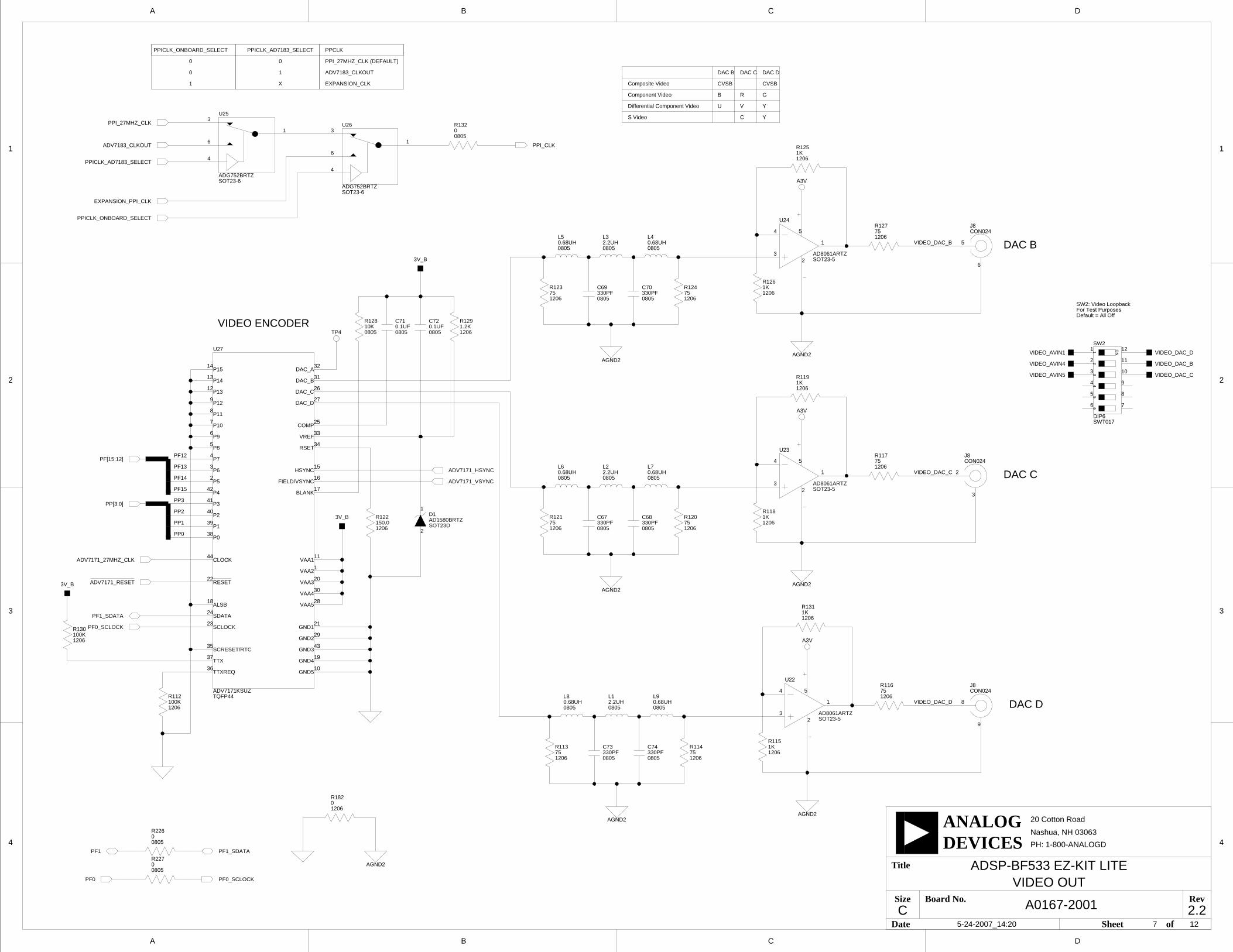
AGND2
AGND2
AGND2AGND2
AGND2
A3V
A3V
D
4
3
2
1
A B C
20 Cotton Road
Nashua, NH 03063
A B C D
4
3
2
1
PH: 1-800-ANALOGD
C
Title
Size Board No.
Date Sheet of
DEVICESANALOG
Rev
ADSP-BF533 EZ-KIT LITE
A0167-2001 2.2
A3V
AGND2
AGND2
P15
P14
P13
P12
P11
P10
P9
P8
P7
P6
P5
P4
P3
P2
P1
P0
CLOCK
RESET
ALSB
SDATA
SCLOCK
SCRESET/RTC
TTX
TTXREQ
DAC_A
DAC_B
DAC_C
DAC_D
COMP
VREF
RSET
HSYNC
FIELD/VSYNC
BLANK
VAA1
VAA2
VAA3
VAA4
VAA5
GND1
GND2
GND3
GND4
GND5
12
45
6
ON
3
For Test PurposesDefault = All Off
0
PPICLK_ONBOARD_SELECT
0
PPICLK_AD7183_SELECT
0
1
1 X
PPCLK
PPI_27MHZ_CLK (DEFAULT)
ADV7183_CLKOUT
EXPANSION_CLK CVSB
Component Video
S Video
Composite Video
Differential Component Video
DAC D
CVSB
GRB
C Y
U V Y
DAC B DAC C
DAC B
DAC C
DAC D
VIDEO ENCODER
SW2: Video Loopback
1
2
3
4
5
6 7
8
9
10
11
12
SWT017DIP6
SW2
5
6
J8CON024
3
2
J8CON024
8
9
J8CON024
VIDEO_AVIN1
1
2
5
3
4
U23
SOT23-5AD8061ARTZ
PF1_SDATAPF1
PF0_SCLOCKPF0
R22600805
12060R182
PF0_SCLOCK
PF1_SDATA
3V_B
TP4
14
13
12
9
8
7
6
5
4
3
2
42
41
40
39
38
44
22
18
24
23
35
37
36
32
31
26
27
25
33
34
15
16
17
11
1
20
30
28
21
29
43
19
10
U27
TQFP44ADV7171KSUZ
PPI_CLK
PPI_27MHZ_CLK
ADV7183_CLKOUT
08050R132
2.2UH0805
L2
0.1UF0805
C72
ADV7171_RESET
150.01206
R122
1
2
D1
SOT23DAD1580BRTZ
0805330PFC74
4
6
3
1
U26
SOT23-6ADG752BRTZ
2.2UH0805
L3
2.2UH0805
L1
08050.68UHL8
0.68UH0805
L9
0.68UH0805
L6
08050.68UHL7
08050.68UHL5
0.68UH0805
L4
3V_B
4
3
5
2
1
U22
SOT23-5AD8061ARTZ
ADV7171_VSYNC
ADV7171_HSYNC
4
3
5
2
1
U24
SOT23-5AD8061ARTZ
10K0805
R128
ADV7171_27MHZ_CLK
VIDEO_DAC_C
VIDEO_DAC_B
VIDEO_DAC_D
7 125-24-2007_14:20
VIDEO OUT
330PF0805
C73
12061KR131
100K1206
R130
12061.2KR129
08050.1UFC71
120675R127
12061KR126
12061KR125
0805330PFC70
751206
R124
120675R123
330PF0805
C69
0805330PFC67
751206
R121
120675R120
330PF0805
C68
1K1206
R119
1K1206
R118
751206
R117
120675R116
12061KR115
751206
R114
120675R113
1206100KR112
PF[15:12]PF12
PF13
PF14
PF15
PP[3:0]PP3
PP2
PP1
PP0
1
3
6
4
U25
SOT23-6ADG752BRTZ
PPICLK_AD7183_SELECT
EXPANSION_PPI_CLK
PPICLK_ONBOARD_SELECT
3V_B
08050R227
VIDEO_AVIN5
VIDEO_AVIN4
VIDEO_DAC_D
VIDEO_DAC_B
VIDEO_DAC_C
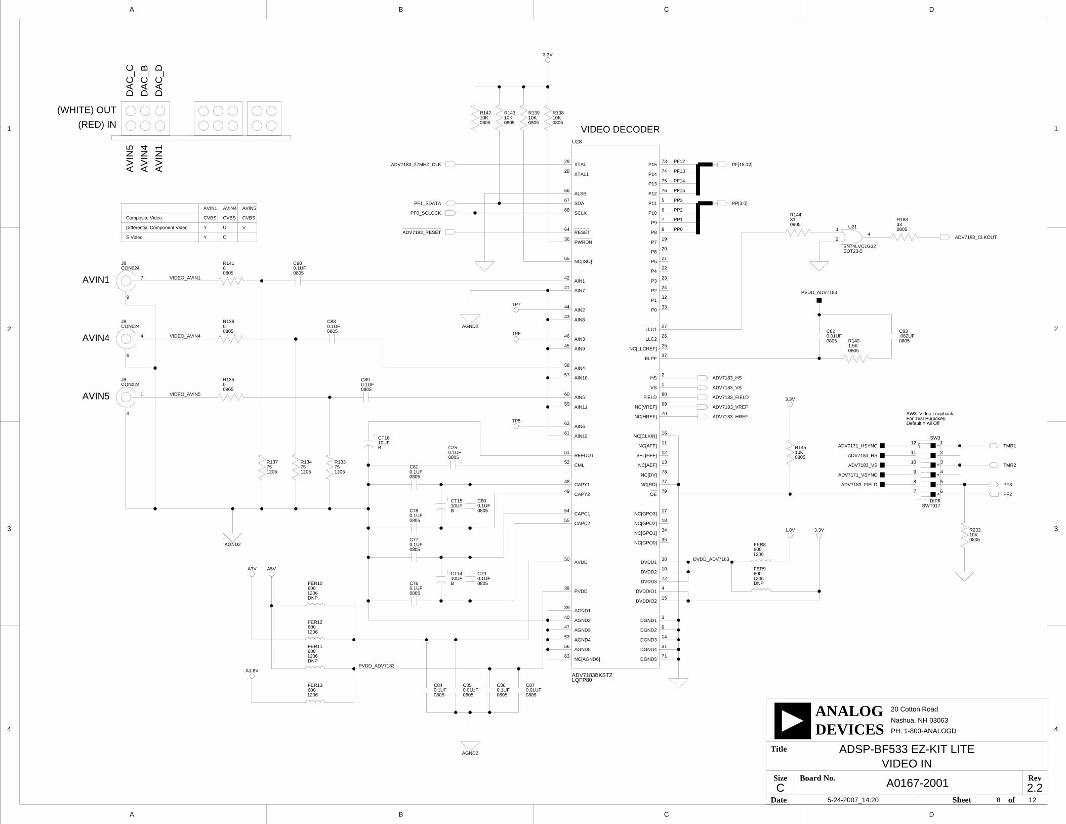
AGND2
AGND2
A5V
3.3V
D
4
3
2
1
A B C
20 Cotton Road
Nashua, NH 03063
A B C D
4
3
2
1
PH: 1-800-ANALOGD
C
Title
Size Board No.
Date Sheet of
DEVICESANALOG
Rev
ADSP-BF533 EZ-KIT LITE
A0167-2001 2.2
3.3V
3.3V
A3V
1.8V
A1.8V
AGND2
12
45
6
ON
3
AGND1
AGND2
AGND3
AGND4
AGND5
AIN1
AIN10
AIN11
AIN12
AIN2
AIN3
AIN4
AIN5
AIN6
AIN7
AIN8
AIN9
ALSB
AVDD
CAPC1
CAPC2
CAPY1
CAPY2
CML
DGND1
DGND2
DGND3
DGND4
DGND5
DVDD1
DVDD2
DVDD3
DVDDIO1
DVDDIO2
ELPF
FIELD
HS
LLC1
LLC2
NC[AEF]
NC[AFF]
NC[AGND6]
NC[CLKIN]
NC[GPO0]
NC[GPO1]
NC[GPO2]
NC[GPO3]
NC[ISO]
NC[DV]
NC[HREF]
NC[LLCREF]
NC[RD]
NC[VREF]
P0
P1
P10
P11
P12
P13
P14
P15
P2
P3
P4
P5
P6
P7
P8
P9
PVDD
REFOUT
SCLK
SDA
SFL[HFF]
VS
XTAL
XTAL1
OE
PWRDN
RESET
For Test PurposesDefault = All Off
CVBSCVBSComposite Video
AVIN1 AVIN4 AVIN5
Y U V
CYS Video
Differential Component Video
AVIN5
AVIN4
AVIN1
VIDEO DECODER
CVBS
(RED) IN
DA
C_B
DA
C_C
DA
C_D
AV
IN4
AV
IN1
AV
IN5
(WHITE) OUT
SW3: Video Loopback
39
40
47
53
56
42
57
59
61
44
46
58
60
62
41
43
45
66
50
54
55
48
49
52
3
9
14
31
71
30
10
72
4
15
37
80
2
27
26
13
11
63
16
35
34
18
17
65
78
70
25
77
69
33
32
6
5
76
75
74
73
24
23
22
21
20
19
8
7
38
51
68
67
12
1
29
28
79
36
64
U28
ADV7183BKSTZLQFP80
1
2
3
4
5
67
8
9
10
11
12
DIP6SWT017
SW3
1
3
J8CON024
6
4
J8CON024
7
9
J8CON024
ADV7183_CLKOUT
1
24
SOT23-5
U21
SN74LVC1G32
PF2
PF3
TMR1
1206
FER9600
DNP
1206
FER11600
DNP
1206
FER10600
DNP
R232
080510K
10K0805
R145
1206
FER8600
DVDD_ADV7183
1206
FER13600
1206
FER12600
PVDD_ADV7183
08050.01UFC82
0805.082UFC83
1.5K0805
R140
PVDD_ADV7183
R183
080533
330805
R144
08050.01UFC87
0.1UF0805
C86
08050.1UFC84
PF0_SCLOCK
ADV7183_27MHZ_CLK
ADV7183_RESET
10UFB
CT15
B10UFCT16
B10UFCT14
0.01UF0805
C85
ADV7183_VS
ADV7183_FIELD
ADV7183_HS
PF1_SDATA
VIDEO_AVIN5
VIDEO_AVIN4
08050R141
080510KR143
10K0805
R142
0.1UF0805
C8800805
R136
VIDEO_AVIN1
8 125-24-2007_14:20
VIDEO IN
08050.1UFC90
08050.1UFC89
080510KR139
10K0805
R138
0.1UF0805
C81120675R137
08050R135
751206
R134
120675R133
0.1UF0805
C80
0.1UF0805
C79
08050.1UFC78
0.1UF0805
C77
08050.1UFC76
08050.1UFC75
PP2PP[3:0]
PP3
PP1
PP0
PF13PF[15:12]
PF12
PF14
PF15
ADV7183_VREF
ADV7183_HREFTP5
TP6
TP7
TMR2
ADV7171_HSYNC
ADV7183_HS
ADV7183_VS
ADV7171_VSYNC
ADV7183_FIELD
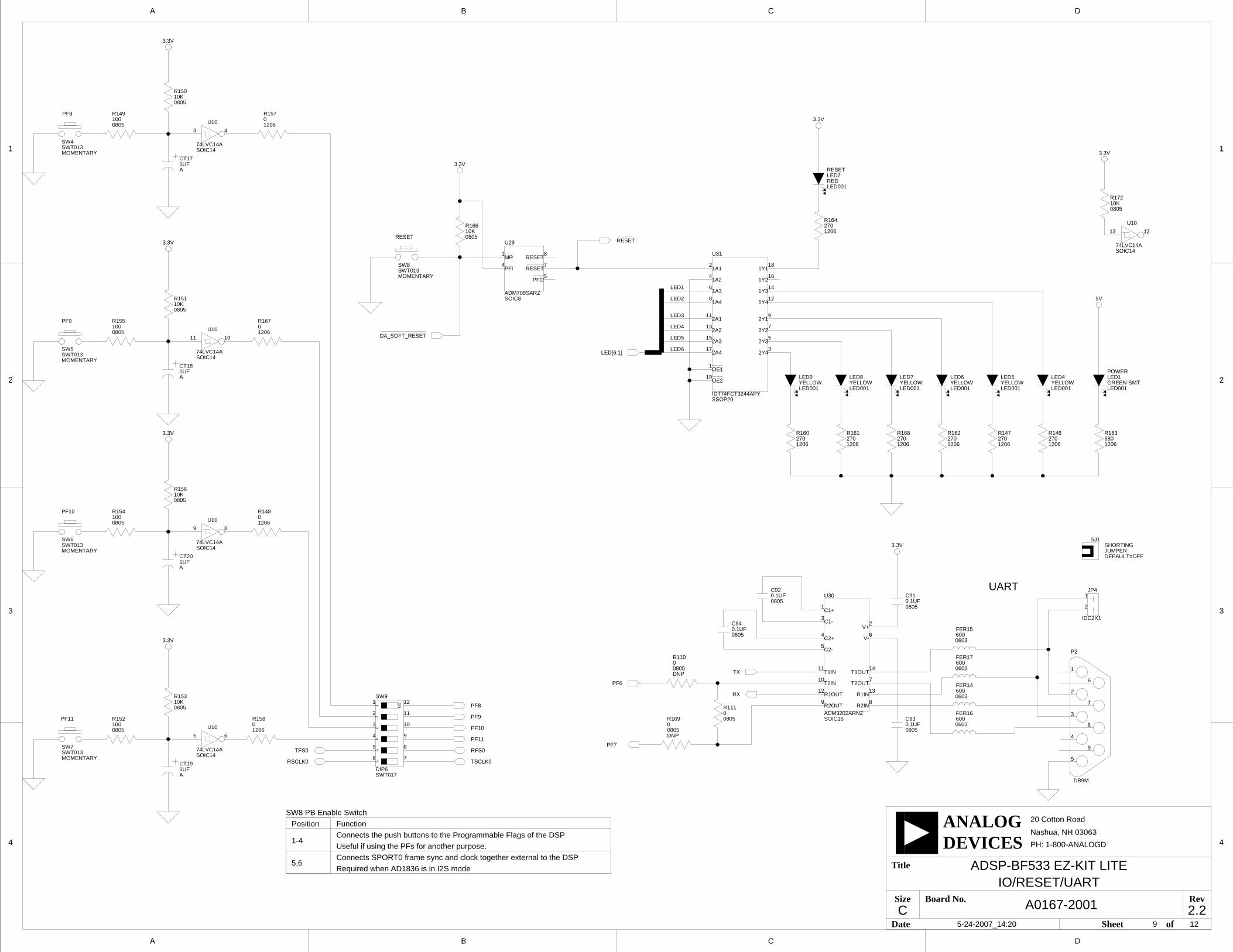
D
4
3
2
1
A B C
20 Cotton Road
Nashua, NH 03063
A B C D
4
3
2
1
PH: 1-800-ANALOGD
C
Title
Size Board No.
Date Sheet of
DEVICESANALOG
Rev
ADSP-BF533 EZ-KIT LITE
A0167-2001 2.2
3.3V
3.3V
3.3V
3.3V
5V
3.3V
3.3V
3.3V
PFI
RESETMR
PFO
RESET
3.3V
C1+
C1-
C2+
C2-
R1INR1OUT
R2INR2OUT
T1OUT
T2IN T2OUT
V-
V+
T1IN
1A1
1A2
1A3
1A4
2A2
2A3
2A4
1Y1
1Y2
1Y3
1Y4
2Y1
2Y2
2A1
2Y4
2Y3
OE1
OE2
12
45
6
ON
3
JUMPERSHORTING
POWER
PF8
PF9
PF10
PF11
RESET
UART
RESET
Required when AD1836 is in I2S mode
FunctionConnects the push buttons to the Programmable Flags of the DSPUseful if using the PFs for another purpose.
Position
1-4
5,6Connects SPORT0 frame sync and clock together external to the DSP
SW8 PB Enable Switch
R110
08050
DNP
00805
R169
DNP
SJ1
DEFAULT=OFF
2
1JP4
IDC2X1
1UFA
CT18
A1UFCT20
1UFA
CT19
RESET
1
2
3
4
5
6 7
8
9
10
11
12
DIP6SWT017
SW9
A1UFCT17
2
4
6
8
13
15
17
18
16
14
12
9
7
11
3
5
1
19
SSOP20
U31
IDT74FCT3244APY
13 12
SOIC14
U10
74LVC14A
11 10
SOIC14
U10
74LVC14A
1
3
4
5
1312
89
14
10 7
6
2
11
U30
SOIC16ADM3202ARNZ
R11100805
3
4
5
1
6
2
7
8
9
P2
DB9M
SWT013MOMENTARY
SW4
MOMENTARYSWT013SW5
SWT013MOMENTARY
SW6
MOMENTARYSWT013SW7
1000805
R152
12060R158
5 6
SOIC14
U10
74LVC14A
0805100R154
01206
R148
89
SOIC14
U10
74LVC14A
TFS0 RFS0
TSCLK0RSCLK0
LED5
LED6LED[6:1]
LED1
LED4
LED2
LED3
YELLOWLED001
LED4
LED001YELLOWLED5
YELLOWLED001
LED6YELLOWLED001
LED7YELLOWLED001
LED8
LED001YELLOWLED9
PF7
PF6
0603
FER16600
0603
FER14600
0603
FER17600
0603
FER15600
1206270R160
08050.1UFC92
4
81
5
7
SOIC8
U29
ADM708SARZ
SWT013MOMENTARY
SW8
0.1UF0805
C94
0.1UF0805
C91
08050.1UFC93
TX
RX
LED001REDLED2
1206270R164
10K0805
R153
1206680R163
GREEN-SMTLED001
LED1
2701206
R146
080510KR166
1206270R168
12060R167
2701206
R1622701206
R161
01206
R157
080510KR156
1000805
R155
43
SOIC14
U10
74LVC14A
10K0805
R151
080510KR150
0805100R149
1206270R147
080510KR172
PF10
PF11
PF8
PF9
DA_SOFT_RESET
9 125-24-2007_14:20
IO/RESET/UART

SHGND
D
4
3
2
1
A B C
20 Cotton Road
Nashua, NH 03063
A B C D
4
3
2
1
PH: 1-800-ANALOGD
C
Title
Size Board No.
Date Sheet of
DEVICESANALOG
Rev
ADSP-BF533 EZ-KIT LITE
A0167-2001 2.2
3.3V
5V 3.3V
5V
3.3V
3V
DA_EMULATOR_TCK
DA_EMULATOR_TDI
DA_EMULATOR_TDO
DA_EMULATOR_TMS
DA_GP0
DA_GP1
DA_GP2
DA_GP3
GN
D
SH
GN
D
TCK
TDI
TDO
TMS
DA_EMULATOR_EMU
DA_EMULATOR_SELECT
DA_EMULATOR_TRST
DA_SOFT_RESET
EMU
RESET
TRST
DEBUG_AGENT
3.3V
All USB interface circuitry is considered proprietary and hasbeen omitted from this schematic.
When designing your JTAG interface please refer to theEngineer to Engineer Note EE-68 which can be found athttp://www.analog.com
DSP JTAG HEADER
EXPANSION INTERFACE (TYPE B)
SPI
SPORT1
DA_EMULATOR_TRST
12060R174
01206
R175
5
2
4
8
10
6
1
3
9
11
13
15
17
19
12
14
16
20
18
7
P3
IDC10X2
R1810K0805
R1610K0805
R1510K0805
DR1PRI
1
3
5
7
9
11
13
2
4
6
8
10
12
14
ZP4
IDC7X2
SCK
MOSI1
3
5
7
9
11
2
4
6
8
10
12
P6
IDC6X2
DT1SEC
TSCLK1
DT1PRI
DR1SEC
10K0805
R173
DA_EMULATOR_SELECT
DA_EMULATOR_TDO
RESET
EMU
TRST
TMS
TDI
TDO
DA_EMULATOR_EMU
DA_EMULATOR_TMS
DA_EMULATOR_TCK
DA_EMULATOR_TDI
CLK_OUT_EXP2
CLK_OUT_EXP1
A1
A2
A18
A16
A14
A12
A10
A8
A6
A4
A19
A17
A15
A13
A11
A9
A7
A5
A3
A[1:19]
PP1
PP3
PF10
PF12
PF14
PF2
PF6
PF8
PF13
PF11
PF9
PF7
PF5
PF3
PF15
PF1PF0
PF4
PF[0:15]
BGH
BG
BR
TFS1
EXT_DSP_CLK
PB6_A
PA6_APA7_A
PB7_A
ADV7183_VREF
ADV7183_FIELD ADV7183_VS
ADV7183_HS
NMI
TX RX
TSCLK0
TSCLK1 RSCLK1
RSCLK0
SCK
EXPANSION_PPI_CLK
PP2
PP0
~ABE1/SDQM1
SRAS
SWE
D[0:15]
D10
D14
D12
D4
D6
D8
D0
D2D3
D5
D7
D9
D11
D13
D15
D1
RESET
5-24-2007_14:20 10 12
CONNECTORS
RESET
MISO
DT1SEC
DT1PRI
TFS1 RFS1
DR1PRI
DR1SEC
ARE
SMS
SCKE
TMR2
TMR0
AMS0
AMS1
AMS2
AMS3
ARDY
~ABE1/SDQM1
AWE
SA10 SCAS
~ABE0/SDQM0
~ABE0/SDQM0
AOE
DR0SEC
DR0PRI
RFS0TFS0
DT0PRI
DT0SEC
TMR1
MOSI
ADV7183_HREF
PA6_B
PA4_B
PA2_B
PA0_B
PA5_B
PA7_B
PA3_B
PA1_B
1
10
1112
1314
1516
1718
19
2
20
2122
2324
2526
2728
29
3
30
3132
3334
3536
3738
39
4
40
4142
4344
4546
4748
49
5
50
5152
5354
5556
5758
59
6
60
6162
6364
6566
6768
69
7
70
7172
7374
7576
7778
79
8
80
8182
8384
8586
8788
89
9
90
CON019
J2 1
10
1112
1314
1516
1718
19
2
20
2122
2324
2526
2728
29
3
30
3132
3334
3536
3738
39
4
40
4142
4344
4546
4748
49
5
50
5152
5354
5556
5758
59
6
60
6162
6364
6566
6768
69
7
70
7172
7374
7576
7778
79
8
80
8182
8384
8586
8788
89
9
90
J3
CON019
1
10
1112
1314
1516
1718
19
2
20
2122
2324
2526
2728
29
3
30
3132
3334
3536
3738
39
4
40
4142
4344
4546
4748
49
5
50
5152
5354
5556
5758
59
6
60
6162
6364
6566
6768
69
7
70
7172
7374
7576
7778
79
8
80
8182
8384
8586
8788
89
9
90
CON019
J1
TCK
DA_SOFT_RESET
MISO
SPISS
SPIS1
RSCLK1
RFS1

PGND
PGND
PGND
1.8V
5V A5V
A1.8V3.3V
D
4
3
2
1
A B C
20 Cotton Road
Nashua, NH 03063
A B C D
4
3
2
1
PH: 1-800-ANALOGD
C
Title
Size Board No.
Date Sheet of
DEVICESANALOG
Rev
ADSP-BF533 EZ-KIT LITE
A0167-2001 2.2
3.3V
OUT1
OUT2
OUT3
IN1
IN2
FBSD GND
OUT1
OUT2
OUT3
IN1
IN2
FBSD GND
A3V
SHGND
GNDINPUT OUTPUT
GNDINPUT OUTPUT
GNDINPUT OUTPUT
3.3V
IN
CS
PGATEFB
COMP
GND
Position
1 and 2
Function
be populated and the DSP_VDD_INT will be hard-wired with R222to use the processor internal regulator.
DSP_VDD_INT = 1.4V Fixed
DSP_VDD_INT = DSP Internal Voltage Regulation
2 and 3
SW10: Core Voltage Source SelectDEFAULT: Not Populated
Note: For boards without a 750MHz processor this jumper will not
D6
4ASSB43L
DO-214AA
D5
1AZHCS1000
SOT23-312
1V4
DO-214AA2A
D2S2A
6
5
2
14
3
U34
FDC658PSOT23-6
2
63
15
4
VR4
ADP1864SOT23-6
08050R186
08050R187
C41UF0805DNP
CT272.2UFBDNP
TP1
C10UFCT22
CT24
C10UF
3
1
2
SOT-223
VR5
ADP3339AKCZ-5 2
1
3
SOT-223
VR1
ADP3338AKCZ-33
2
1
3
VR3
SOT-223ADP3339AKCZ-33
1206
FER20600
C10UFCT21
2ADO-214AA
D4S2A
DO-214AA2A
D3S2A
CT28
D68UF
00805
R222
CT13
C10UF
340.0KR185
0805
L1210UHIND001
3
1
2
IDC3X1
JP3
DNP
TP15
00805
R211
DNP
4
3
2
1
8
7
6
5
U32
SOIC8FDS9431A
DSP_VDD_INT
64.9KR184
0805
08051UFC61
3.32KR223
0805
VROUT
UNREG_IN
08051UFC103
10K0805
R192
10K0805
R214
08051UFC102
147.0KR191
1206
76.8KR190
1206
1
2
3
7
8
56
4MSOP8
VR2
ADP3336ARMZ
1
2
3
7
8
56
4MSOP8
VR6
ADP3336ARMZ
DSP_VDD_INT
DSP_VDD_EXT
4
1
3
2
FER002
FER23190
FUS0012.5AF1
08050R210
08051UFC60
08051UFC104
C105
08050.1UF
00805
R188
12060R177
DSP_VDD_EXT
08050.1UFC98
10UFC
CT230.1UF0805
C175
C1000.1UF0805
01206
R178
UNREG_IN
12061000PFC96
12061000PFC97
1
3
2
CON0057.5V_POWER
J9
11 125-24-2007_14:20
POWER
1206
FER18600
3V_B
1206
FER19600
UNREG_IN
1206100KR176
08050.1UFC143
CT2510UFC
VDDRTC
R171255.0K0603
R17080.6K0603
R1650.051206
R15900603
C6510UF1210
C6468PF0603
C63470PF0603
R1124.9K0603
L106.8UHIND009
C6210UF0805DNP
CT2647UFB
R300805
UNREG_IN
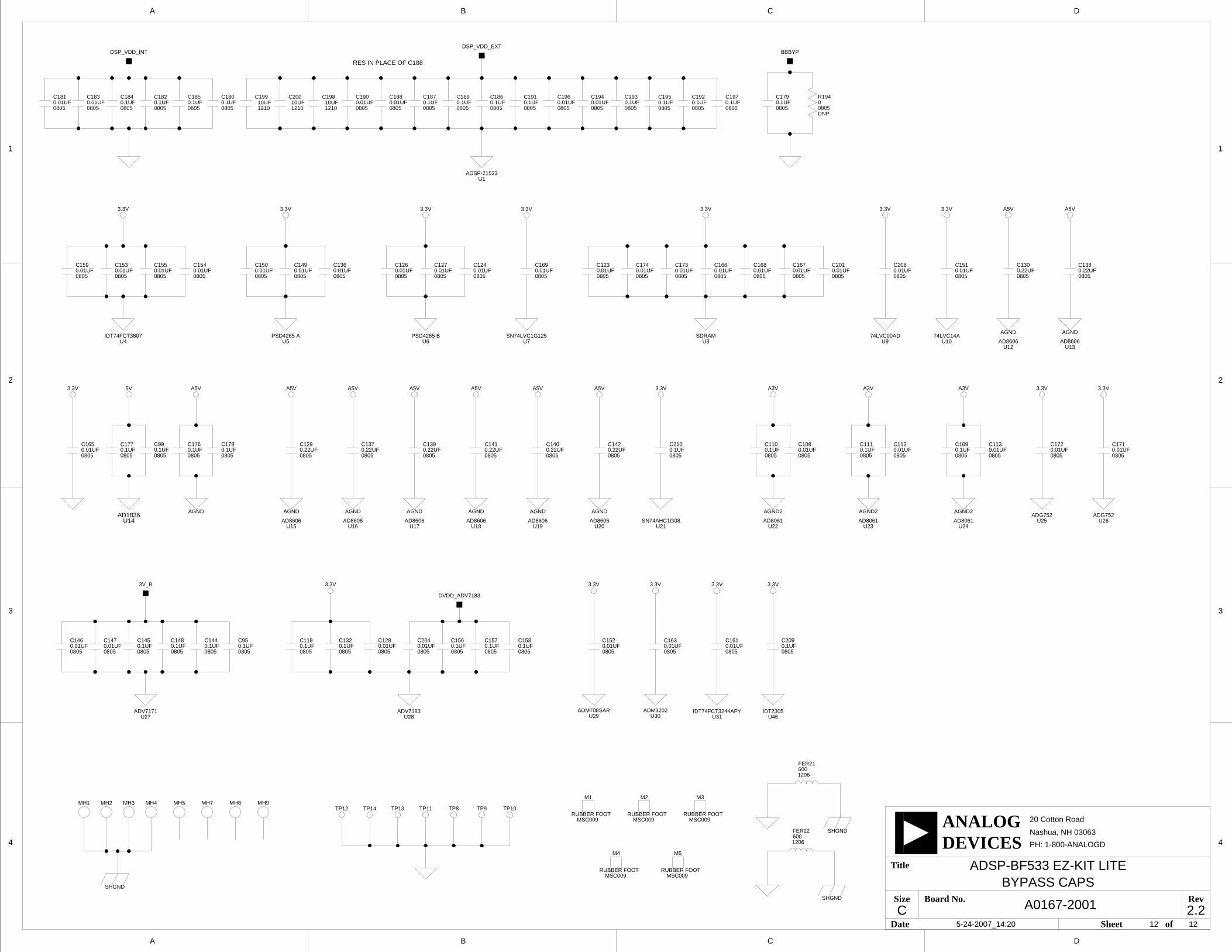
SHGND
SHGND
MSC009RUBBER FOOT
MSC009RUBBER FOOT
MSC009RUBBER FOOT
MSC009RUBBER FOOT
MSC009RUBBER FOOT
SHGND
3.3V
AGND2
3.3V3.3V
3.3V3.3V3.3V3.3V3.3V3.3V
3.3V 3.3V
D
4
3
2
1
A B C
20 Cotton Road
Nashua, NH 03063
A B C D
4
3
2
1
PH: 1-800-ANALOGD
C
Title
Size Board No.
Date Sheet of
DEVICESANALOG
Rev
ADSP-BF533 EZ-KIT LITE
A0167-2001 2.2
A3V A3V A3VA5V A5VA5V
AGND
AGND AGND AGND
A5V
AGND
A5V
AGND
AGND
A5V
AGND
A5V A5V
5V
AGND
A5V
3.3V
3.3V3.3V
3.3V
AGND2AGND2
3.3V
RES IN PLACE OF C188
AD8606 AD8606AD8606AD8606 AD8606 AD8061AD8061U23 U24U22
AD8061U15 U17U16 U20U18
U4IDT74FCT3807
ADG752 ADG752U26U25
U30ADM3202
U29ADM708SARADV7171
U27ADV7183
U28IDT74FCT3244APY
U31
AD1836U14
PSD4265 AU5
PSD4265 BU6
SN74LVC1G125U7
SDRAMU8
74LVC00ADU9
74LVC14AU10 AD8606
U12AD8606
U13
ADSP-21533
AD8606U19
IDT2305U46
U21SN74AHC1G08
U1
08050R194
DNP
08050.01UFC127
08050.01UFC188
08050.01UFC190
DSP_VDD_EXT
08050.01UFC146
0.01UF0805
C1470.1UF0805
C145
08050.1UFC148
0.1UF0805
C1440.1UF0805
C95
08050.1UFC119
08050.1UFC132
0.01UF0805
C128 C204
08050.01UF
08050.1UFC156
0.1UF0805
C157
08050.1UFC158
0.01UF0805
C1520.01UF0805
C1630.01UF0805
C161
08050.01UFC171
08050.01UFC172
08050.01UFC113
08050.1UFC109C112
08050.01UF0.1UF
0805
C1110.01UF0805
C108
08050.1UFC110
0.22UF0805
C1420.22UF0805
C1400.22UF0805
C1410.22UF0805
C1390.22UF0805
C1370.22UF0805
C1290.1UF0805
C178
08050.1UFC176
08050.1UFC99
08050.1UFC177
0.01UF0805
C165
0.22UF0805
C138
08050.22UFC130
0.01UF0805
C151C208
08050.01UF
C201
08050.01UF
08050.01UFC167
08050.01UFC168
08050.01UFC166
08050.01UFC173
0.01UF0805
C1740.01UF0805
C1230.01UF0805
C1690.01UF0805
C124
08050.01UFC126
0.01UF0805
C136
08050.01UFC149
08050.01UFC150C154
08050.01UF0.01UF
0805
C155
08050.01UFC153
0.01UF0805
C159
0.1UF0805
C197
08050.1UFC192
0.1UF0805
C195
08050.1UFC193
08050.01UFC194
0.01UF0805
C196
08050.1UFC191
0.1UF0805
C186
08050.1UFC189
0.1UF0805
C18710UF1210
C19810UF1210
C200
121010UF
C1990.01UF0805
C181
08050.01UFC183
08050.1UFC184
0.1UF0805
C182
08050.1UFC185
0.1UF0805
C180
08050.1UFC179
12 125-24-2007_14:20
BYPASS CAPS
BBBYPDSP_VDD_INT
DVDD_ADV7183
3V_B
08050.1UFC209
C2100.1UF0805
M1
M4 M5
M3M2MH9MH8MH7MH5MH3MH2 MH4MH1
TP11 TP10TP8
1206
FER21600
1206
FER22600
TP9TP14 TP13TP12
ADSP-BF533 EZ-KIT Lite Evaluation System Manual I-1
I INDEX
AAD1836 audio codec, xii, 1-18, 1-20, 2-4,
2-11ADV7171 video encoder, xi, 1-21, 2-6,
2-7, 2-10ADV7183 video decoder, xi, 1-21, 2-6,
2-7, 2-10AINx analog video channels, 2-7AMS2-0 memory select pins, 1-12, 1-15,
2-3analog
audio interface, See SPORT0, SPORT1video interface, See video interface
architecture, of this EZ-KIT Lite, 2-2ASYNC (asynchronous memory control)
control registers, 1-16external memory banks 0-2, 1-12, 1-15
audiocodecs, See AD1836 audio codecsconnectors (J4-5), 2-17
Bbill of materials, A-1board design database, 1-22board schematic (ADSP-BF533), B-1boot mode switch (SW11), 2-10
CCCLK pin, 1-14clock
frequency, 1-13in (CLK IN) signal, 2-7out (CLK OUT) signal, 2-3
codecs, See 1836 audio codecsconfiguration, of this EZ-KIT Lite, 1-3connectors
diagram of locations, 1-3, 2-16DB9 (UART), 2-7, 2-19J1-3 (expansion interface), 2-8, 2-17J4-5 (audio), 2-17J8 (video), 2-18J9 (power), 1-4, 2-18P1 (FlashLINK), 2-19P2 (RS-232), 2-7, 2-19P3 (SPORT1), 2-4, 2-20P6 (SPI), 2-4, 2-12, 2-21ZP4 (JTAG), 2-8, 2-20
contents, of this EZ-KIT Lite package, 1-3core
frequency, 1-14voltage, 2-2
DDAC analog video channels, 2-7Data In/Out registers, 1-17DB9 (UART) connector, 2-7, 2-19default configuration, of this EZ-KIT Lite,
1-3
Index
I-2 ADSP-BF533 EZ-KIT Lite Evaluation System Manual
DIP switchesdiagram of locations, 1-3SW1-2 (test), 2-10SW3 (video config), 1-21, 2-7, 2-10SW9 (push button enable), 1-20, 2-11,
2-13Direction registers, 1-17
EEBIU, See external bus interface unitEBIU_AMBCTLx registers, 1-16EBIU_SDx registers, 1-14evaluation license
CCES, 1-10example programs, 1-22expansion interface, 2-3, 2-4, 2-7, 2-8, 2-17external bus interface unit (EBIU), 2-3external memory
See also flash memories, SDRAM, ASYNC
via JTAG, 2-8
Ffeatures, of this EZ-KIT Lite, xiFIELD pin, 2-4, 2-7, 2-11flag pins, See programmable flags (PFs)flash A
configuration registers, 1-16, 1-17port A controls, 1-18port B controls, 1-18primary/secondary/SRAM, 1-16
flash Bconfiguration registers, 1-16, 1-18primary/secondary/SRAM, 1-16
FlashLINK connector (P7), 2-19
flash memoriesSee also flash A, flash Bconfiguration registers, 1-12EBIU connection, 2-3general-purpose IO pins, 1-15, 1-16,
2-15, 2-20internal SRAM, 1-12primary/secondary, 1-12, 1-15, 2-3reserved, 1-16
flash ports (PB5-0), 2-15frequency, 1-13, 1-14
Ggeneral-purpose IO pins, 1-15, 1-16, 1-19,
1-20GND signal, 2-8, 2-18
HHSYNC signal, 2-6, 2-7, 2-10
Iinstallation, of this EZ-KIT Lite, 1-9
CCES, 1-5interfaces, See video, SPORT, PPI, SPI,
expansioninternal memory
core MMRs, 1-13data banks A, B (SRAM), 1-13instruction SRAM, 1-13instruction SRAM/CACHE, 1-13reserved, 1-13scratch pad SRAM, 1-13system MMRs, 1-13via JTAG, 2-8
IOport registers, 1-17voltage, 2-2
ADSP-BF533 EZ-KIT Lite Evaluation System Manual I-3
Index
JJTAG
connector (ZP4), 2-20emulation port, 2-8
jumpersdiagram of locations, 2-9default settings, 1-3
LLEDs
diagram of locations, 1-3, 2-12LED1 (power), 1-4, 2-14LED2 (reset), 1-4, 2-14LED4-9 (general-purpose IO), 1-19,
2-15ZLED3 (USB monitor), 1-9, 2-15
license restrictions, 1-11
MMedia Instruction Set Computing (MISC),
ixmemory
map, of this EZ-KIT Lite, 1-12, 1-16select pins, See AMS2-0, SMS0
Micro Signal Architecture (MSA), ixMSB pin, 2-5, 2-6
Nnotation conventions, xviii
Ooscillators, 1-18
Ppackage contents, 1-3parallel peripheral interface (PPI), 1-18,
1-21, 2-5, 2-7, 2-10
powerconnector (J9), 2-18specifications, 2-18
PPI7-0 pins, 2-6PPI_CLK pin, 1-18, 2-6PPI_FSYNC signal, 2-6PPI_HSYNC signal, 2-6primary memory, See flash memories, flash
A, flash Bprogrammable flags (PFs)
connections, 2-4PF0 (serial clock), 1-21, 2-4PF12-15 (PPI7-4 and video MSB signal),
2-5, 2-6PF1 (serial data), 1-21, 2-4PF2 (ADV7183 OE signal), 1-21, 2-4,
2-10PF3 (ADV7183 FIELD pin), 2-4, 2-6,
2-11PF4 (AD1836 SPI select), 1-20, 2-4PF5-7 (PPI14-12), 2-5PF8-11 (PPI11-8 and SW4-7), 1-19,
2-5, 2-11, 2-14push buttons
See also switches by name (SWx)diagram of locations, 2-12
RRCA jacks, xi, 2-17Reduced Instruction Set Computing
(RISC), ixreset
AD1836 codec, 1-18ADV7171/ADV7183 decoder/encoder,
1-18LED (LED2), 2-14processor, 1-13, 1-15, 1-17push button (SW8), 2-14
restrictions, of the licence, 1-11RFS0 pin, 1-20, 2-12
Index
I-4 ADSP-BF533 EZ-KIT Lite Evaluation System Manual
RS-232 connector (P2), xi, 2-7, 2-19RSCLK0 pin/register, 1-20, 2-12
Sschematic, of ADSP-BF533 EZ-KIT Lite,
B-1SCLK pin, 1-14SDRAM
connection, 2-3interface, 1-12, 1-13optimum settings, 1-14
secondary memory, See flash memories, flash A, flash B
serialclock (SCL), 1-21data (SDAT), 1-21
serial peripheral interface (SPI)connector (P6), 2-4, 2-12, 2-21other connections, 2-8port, 1-20
setup, of this EZ-KIT Lite, 1-3SMS0 memory select pin, 1-12, 2-3SPIS1/SPISS select switch (SW10), 2-12SPORT0
frame sync/clock signals, 2-11interface, 2-3, 2-8switch (SW12), 2-12
SPORT1connector (P3), 2-20interface, 2-4, 2-8
SPORT audio interface, 1-20SRAM (internal flash memory), 1-12, 2-3startup, of this EZ-KIT Lite, 1-9
CCES, 1-5SW10 (SPIS1/SPISS select) switch, 2-12SW11 (boot mode) switch, 2-10SW12 (SPORT0) switch, 2-12SW1-2 (test) DIP switches, 2-10
SW3 (video config) DIP switch, 1-21, 2-7, 2-10
SW4-7 (general input) push buttons, 1-19, 2-5, 2-11, 2-14
SW8 (reset) push button, 2-14SW9 (push button enable) DIP switch,
1-20, 2-11, 2-13switches
See also switches by name (SWx)diagram of locations, 2-9
synchronous dynamic random access memory, See SDRAM
systemarchitecture, 2-2clock register (SCLK), 1-13
Ttechnical support, xvtest DIP switches (SW1-2), 2-10TFS0 pin, 1-20, 2-12time-division multiplexed (TDM) mode,
1-20TMR0 pin, 2-8TMR2-1 pins, 2-6, 2-8, 2-10TSCLK0 pin/register, 1-20, 2-12two-wire interface (TWI) mode, 1-20
UUART
loop jumper (JP4), 2-9port, xi, 2-7, 2-8
universal asynchronous receiver transmitter, See UART
USBcable, 1-3, 1-4interface chip (U34), 2-14monitor LED (ZLED3), 2-15
user LEDs (LED4-9), 1-19, 2-15
ADSP-BF533 EZ-KIT Lite Evaluation System Manual I-5
Index
Vvery-long instruction word (VLIW), ixvideo
configuration switch (SW3), 2-10connector (J8), 2-18control signals, 2-8decoders, See ADV7171encoders, See ADV7183input mode, 2-7interface, 1-21output mode, 2-7
VisualDSP++environment, 1-9
voltage regulators, 1-14VSYNC signal, 2-6, 2-7, 2-11


