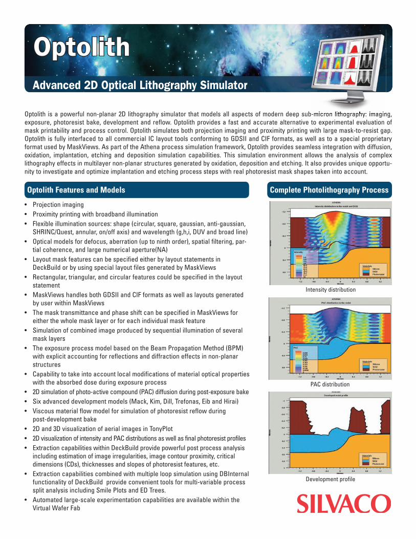
Optolith is a powerful non-planar 2D lithography simulator that models all aspects of modern deep sub-micron lithography: imaging, exposure, photoresist bake, development and reflow. Optolith provides a fast and accurate alternative to experimental evaluation of mask printability and process control. Optolith simulates both projection imaging and proximity printing with large mask-to-resist gap. Optolith is fully interfaced to all commercial IC layout tools conforming to GDSII and CIF formats, as well as to a special proprietary format used by MaskViews. As part of the Athena process simulation framework, Optolith provides seamless integration with diffusion, oxidation, implantation, etching and deposition simulation capabilities. This simulation environment allows the analysis of complex lithography effects in multilayer non-planar structures generated by oxidation, deposition and etching. It also provides unique opportu- nity to investigate and optimize implantation and etching process steps with real photoresist mask shapes taken into account. • Projection imaging • Proximity printing with broadband illumination • Flexible illumination sources: shape (circular, square, gaussian, anti-gaussian, SHRINC/Quest, annular, on/off axis) and wavelength (g,h,i, DUV and broad line) • Optical models for defocus, aberration (up to ninth order), spatial filtering, par- tial coherence, and large numerical aperture(NA) • Layout mask features can be specified either by layout statements in DeckBuild or by using special layout files generated by MaskViews • Rectangular, triangular, and circular features could be specified in the layout statement • MaskViews handles both GDSII and CIF formats as well as layouts generated by user within MaskViews • The mask transmittance and phase shift can be specified in MaskViews for either the whole mask layer or for each individual mask feature • Simulation of combined image produced by sequential illumination of several mask layers • The exposure process model based on the Beam Propagation Method (BPM) with explicit accounting for reflections and diffraction effects in non-planar structures • Capability to take into account local modifications of material optical properties with the absorbed dose during exposure process • 2D simulation of photo-active compound (PAC) diffusion during post-exposure bake • Six advanced development models (Mack, Kim, Dill, Trefonas, Eib and Hirai) • Viscous material flow model for simulation of photoresist reflow during post-development bake • 2D and 3D visualization of aerial images in TonyPlot • 2D visualization of intensity and PAC distributions as well as final photoresist profiles • Extraction capabilities within DeckBuild provide powerful post process analysis including estimation of image irregularities, image contour proximity, critical dimensions (CDs), thicknesses and slopes of photoresist features, etc. • Extraction capabilities combined with multiple loop simulation using DBInternal functionality of DeckBuild provide convenient tools for multi-variable process split analysis including Smile Plots and ED Trees. • Automated large-scale experimentation capabilities are available within the Virtual Wafer Fab Intensity distribution PAC distribution Development profile Optolith Advanced 2D Optical Lithography Simulator Optolith Features and Models Complete Photolithography Process
Transcript
Optolith is a powerful non-planar 2D lithography simulator that models all aspects of modern deep sub-micron lithography: imaging, exposure, photoresist bake, development and reflow. Optolith provides a fast and accurate alternative to experimental evaluation of mask printability and process control. Optolith simulates both projection imaging and proximity printing with large mask-to-resist gap. Optolith is fully interfaced to all commercial IC layout tools conforming to GDSII and CIF formats, as well as to a special proprietary format used by MaskViews. As part of the Athena process simulation framework, Optolith provides seamless integration with diffusion, oxidation, implantation, etching and deposition simulation capabilities. This simulation environment allows the analysis of complex lithography effects in multilayer non-planar structures generated by oxidation, deposition and etching. It also provides unique opportu-nity to investigate and optimize implantation and etching process steps with real photoresist mask shapes taken into account.
SHRINC/Quest, annular, on/off axis) and wavelength (g,h,i, DUV and broad line) • Optical models for defocus, aberration (up to ninth order), spatial filtering, par-
tial coherence, and large numerical aperture(NA) • Layout mask features can be specified either by layout statements in
DeckBuild or by using special layout files generated by MaskViews• Rectangular, triangular, and circular features could be specified in the layout
statement• MaskViews handles both GDSII and CIF formats as well as layouts generated
by user within MaskViews• The mask transmittance and phase shift can be specified in MaskViews for
either the whole mask layer or for each individual mask feature • Simulation of combined image produced by sequential illumination of several
mask layers• The exposure process model based on the Beam Propagation Method (BPM)
with explicit accounting for reflections and diffraction effects in non-planar structures
• Capability to take into account local modifications of material optical properties with the absorbed dose during exposure process
• 2D simulation of photo-active compound (PAC) diffusion during post-exposure bake• Six advanced development models (Mack, Kim, Dill, Trefonas, Eib and Hirai) • Viscous material flow model for simulation of photoresist reflow during
post-development bake • 2D and 3D visualization of aerial images in TonyPlot • 2D visualization of intensity and PAC distributions as well as final photoresist profiles• Extraction capabilities within DeckBuild provide powerful post process analysis
including estimation of image irregularities, image contour proximity, critical dimensions (CDs), thicknesses and slopes of photoresist features, etc.
• Extraction capabilities combined with multiple loop simulation using DBInternal functionality of DeckBuild provide convenient tools for multi-variable process split analysis including Smile Plots and ED Trees.
• Automated large-scale experimentation capabilities are available within the Virtual Wafer Fab
Intensity distribution
PAC distribution
Development profile
OptolithAdvanced 2D Optical Lithography Simulator
Optolith is a powerful non-planar 2D lithography simulator that models all aspects of modern deep sub-micron lithography: imaging,
Optolith Features and Models Complete Photolithography Process
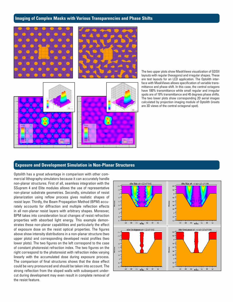
The two upper plots show MaskViews visualization of GDSII layouts with regular (hexagons) and irregular shapes. These are test layouts for an LCD application. The Optolith inter-face with MaskViews allows specification of variable trans-mittance and phase shift. In this case, the central octagons have 100% transmittance while small regular and irregular spots are of 19% transmittance and 45 degrees phase shifts. The two lower plots show corresponding 2D aerial images calculated by projection imaging module of Optolith (insets are 3D views of the central octagonal spot).
Optolith has a great advantage in comparison with other com-mercial lithography simulators because it can accurately handle non-planar structures. First of all, seamless integration with the SSuprem 4 and Elite modules allows the use of representative non-planar substrate geometries. Secondly, simulation of resist planarization using reflow process gives realistic shapes of resist layer. Thirdly, the Beam Propagation Method (BPM) accu-rately accounts for diffraction and multiple reflection effects in all non-planar resist layers with arbitrary shapes. Moreover, BPM takes into consideration local changes of resist refraction properties with absorbed light energy. This example demon-strates these non-planar capabilities and particularly the effect of exposure dose on the resist optical properties. The figures above show intensity distributions in a non-planar structure (two upper plots) and corresponding developed resist profiles (two lower plots). The two figures on the left correspond to the case of constant photoresist refraction index. The two figures on the right correspond to the photoresist with refraction index varying linearly with the accumulated dose during exposure process. The comparison of final structures shows that the dose effect could be very pronounced and should be taken into account. The strong reflection from the sloped walls with subsequent under-cut during development may even result in complete removal of the resist feature.
Imaging of Complex Masks with Various Transparencies and Phase Shifts
Exposure and Development Simulation in Non-Planar Structures
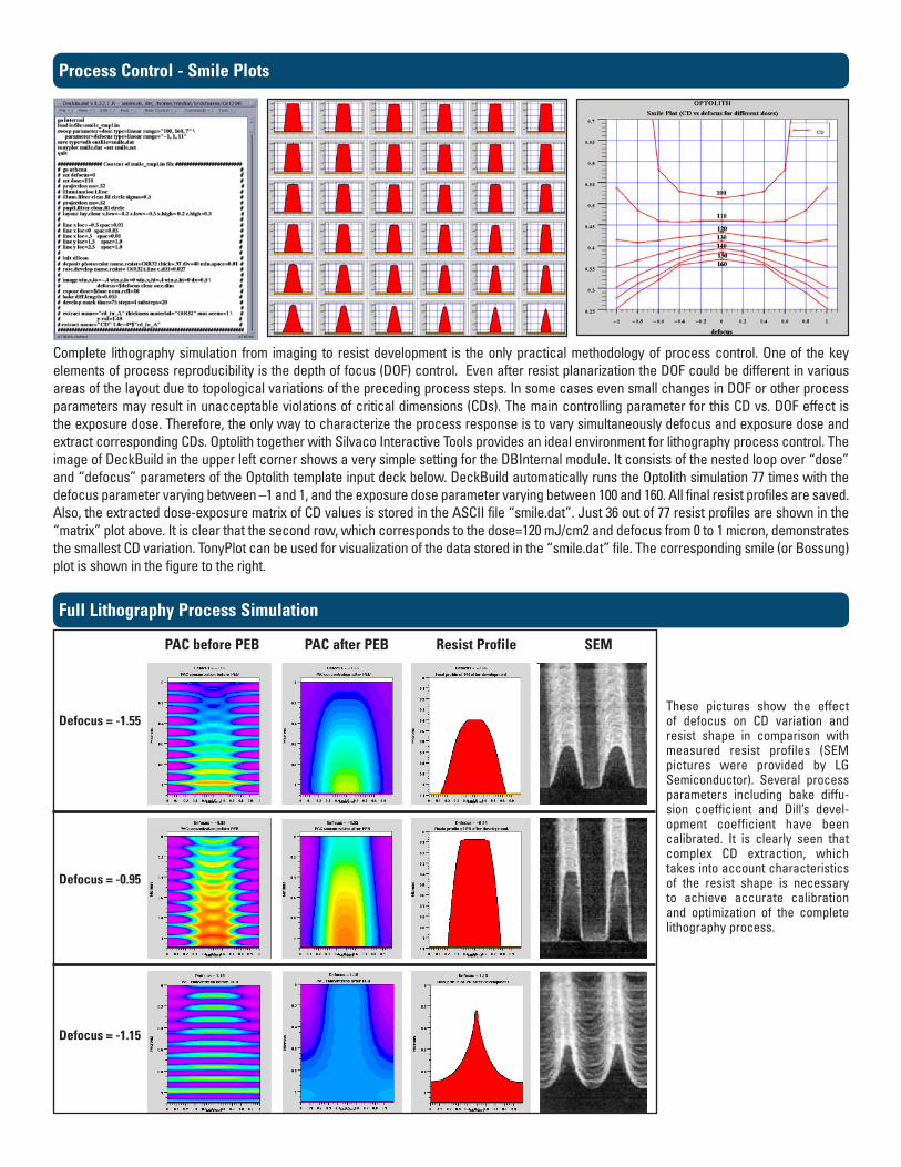
Complete lithography simulation from imaging to resist development is the only practical methodology of process control. One of the key elements of process reproducibility is the depth of focus (DOF) control. Even after resist planarization the DOF could be different in various areas of the layout due to topological variations of the preceding process steps. In some cases even small changes in DOF or other process parameters may result in unacceptable violations of critical dimensions (CDs). The main controlling parameter for this CD vs. DOF effect is the exposure dose. Therefore, the only way to characterize the process response is to vary simultaneously defocus and exposure dose and extract corresponding CDs. Optolith together with Silvaco Interactive Tools provides an ideal environment for lithography process control. The image of DeckBuild in the upper left corner shows a very simple setting for the DBInternal module. It consists of the nested loop over “dose” and “defocus” parameters of the Optolith template input deck below. DeckBuild automatically runs the Optolith simulation 77 times with the defocus parameter varying between –1 and 1, and the exposure dose parameter varying between 100 and 160. All final resist profiles are saved. Also, the extracted dose-exposure matrix of CD values is stored in the ASCII file “smile.dat”. Just 36 out of 77 resist profiles are shown in the “matrix” plot above. It is clear that the second row, which corresponds to the dose=120 mJ/cm2 and defocus from 0 to 1 micron, demonstrates the smallest CD variation. TonyPlot can be used for visualization of the data stored in the “smile.dat” file. The corresponding smile (or Bossung) plot is shown in the figure to the right.
These pictures show the effect of defocus on CD variation and resist shape in comparison with measured resist profiles (SEM pictures were provided by LG Semiconductor). Several process parameters including bake diffu-sion coefficient and Dill’s devel-opment coefficient have been calibrated. It is clearly seen that complex CD extraction, which takes into account characteristics of the resist shape is necessary to achieve accurate calibration and optimization of the complete lithography process.
PAC before PEB PAC after PEB Resist Profile SEM
Defocus = -1.55
Defocus = -0.95
Defocus = -1.15
Process Control - Smile Plots
Full Lithography Process Simulation
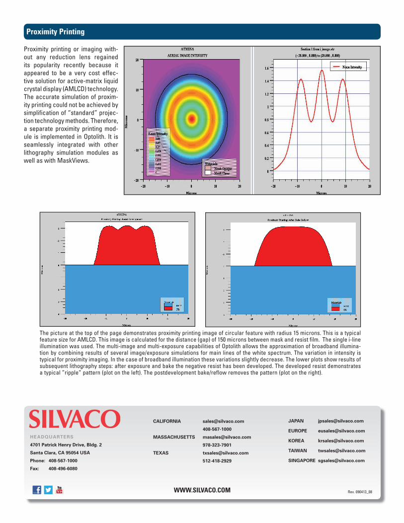
Proximity printing or imaging with-out any reduction lens regained its popularity recently because it appeared to be a very cost effec-tive solution for active-matrix liquid crystal display (AMLCD) technology. The accurate simulation of proxim-ity printing could not be achieved by simplification of “standard” projec-tion technology methods. Therefore, a separate proximity printing mod-ule is implemented in Optolith. It is seamlessly integrated with other lithography simulation modules as well as with MaskViews.
The picture at the top of the page demonstrates proximity printing image of circular feature with radius 15 microns. This is a typical feature size for AMLCD. This image is calculated for the distance (gap) of 150 microns between mask and resist film. The single i-line illumination was used. The multi-image and multi-exposure capabilities of Optolith allows the approximation of broadband illumina-tion by combining results of several image/exposure simulations for main lines of the white spectrum. The variation in intensity is typical for proximity imaging. In the case of broadband illumination these variations slightly decrease. The lower plots show results of subsequent lithography steps: after exposure and bake the negative resist has been developed. The developed resist demonstrates a typical ”ripple” pattern (plot on the left). The postdevelopment bake/reflow removes the pattern (plot on the right).
![2 LASER INTERFERENCE LITHOGRAPHY - uni-halle.de · 2 LASER INTERFERENCE LITHOGRAPHY (LIL) 9 2 LASER INTERFERENCE LITHOGRAPHY (LIL) Laser interference lithography [3~22] (LIL) is a](https://static.documents.pub/doc/80x56/5eae180eecc7e273a41a4e88/2-laser-interference-lithography-uni-hallede-2-laser-interference-lithography.jpg)


