Page 1
Advanced Antenna Miniaturization Techniques for
Low-Power, Broadband and Diversity Wireless Systems
by
Jungsuek Oh
A dissertation submitted in partial fulfillment
of the requirements for the degree of
Doctor of Philosophy
(Electrical Engineering)
in The University of Michigan
2012
Doctoral Committee:
Professor Kamal Sarabandi, Chair
Professor Christopher Ruf
Professor Amir Mortazawi
Professor Eric Michielssen
Page 2
© Jungsuek Oh 2012
All Rights Reserved
Page 3
ii
To God
To my father Sehoon and my mother Kwangja
To my wife Hyesook and my lovely son Yeonjun
Page 4
iii
ACKNOWLEDGEMENTS
First and foremost, I would like to thank and dedicate all my success to God, my
parents and parents-in-law. Without their love and care, I would not be able to
accomplish this dissertation.
I want to express my sincere gratitude and appreciation to my advisors Prof.
Kamal Sarabandi for his warm heart, continuous support, encouragement and guidance
throughout my studies. I could not have imagined having a better advisor and mentor for
my Ph.D study. I would like to extend my sincere gratitude to my other committee
members, Prof. Christopher Ruf, Prof. Amir Mortazawi and Prof. Eric Michielssen for
devoting their time to review this thesis and advising me with valuable suggestions.
I am also grateful to Prof. Sangwook Nam at Seoul National University for his
support and guidance during my master's program. I was able to have a solid background
in applied electromagnetics and microwave engineering at his group.
This list will not be complete without acknowledging my wife Hyesook for her
support during the past four years. If at all I am successful in life, it is not sheer luck or
my brilliance; it is all my loving wife Hyesook's support and endless love. Presence of
my lovely son Yeonjun, who was born in October 2010 and brought a great deal of joy
into my life, was also a great motivation for me.
Page 5
iv
I would like to thank my colleagues and friends at the Radiation Laboratory and
EECS for constructive and insightful discussions. I thank Prof. Mahta Moghaddam, Prof.
Anthony Grbic, Prof. Mona Jarrahi, Dr. Adib Nashashibi, Dr. Michael Thiel, Dr. Wonbin
Hong, Dr. Juseop Lee, Dr. Mehrnoosh Vahidpoor, Dr. Adel Elsherbini, Dr. Jacquelyn A.
Vitaz, Dr. Farhad Bayatpur, Dr. Amelia Marie Buerkle, Dr. Xueyang Duan, Dr. Mark
Haynes, Dr. Mortaza Nick, Dr. Scott Rudolph, Dr. Onur Bakir, Dr. DaHan Liao, Fikadu
Dagefu, Kyusang Lee, Youngjun Song, Sangjo Choi, Michael Benson, Meysam Moallem,
Hatim Bukhari, Jihun Choi, Abdulkadir Yucel, Victor Lee, Seyit Ahmet Sis, Mani
Kashanianfard, Hamid Nejatie, Jiangfeng Wu, Carl Pfeiffer, Mohammad Faghih Imani,
Amit Patel, Seungku Lee, Taehee Jang, Hyeongseok Kim, …
Finally, I would like to thank my friends and Pastor Sang Park at Campus Town
Church of Ann Arbor.
I would like to acknowledge the financial support that I received from the Center
for Objective Microelectronics and Biomimetic Adaptive Technology (COMBAT),
which facilitated my research and my graduate life in the first three years of my studies. I
am also thankful to the Rackham School of Graduate Studies for awarding me the
Rackham Predoctoral Fellowship that generously funded the final year of my Doctoral
research during the 2011-2012 academic years.
Jungsuek
Summer, 2012,
Ann Arbor.
Page 6
v
TABLE OF CONTENTS
DEDICATION................................................................................................................... ii
ACKNOWLEDGEMENTS ............................................................................................ iii
LIST OF FIGURES ....................................................................................................... viii
LIST OF TABLES ........................................................................................................ xvii
LIST OF APPENDICS ................................................................................................ xviii
ABSTRACT .................................................................................................................... xix
CHAPTER
1. Introduction ........................................................................................................1
1.1. Motivation .............................................................................................1
1.2. Current State of the Art .........................................................................4
1.3. Dissertation Overview ..........................................................................8
2. Design of Electrically Short Monopole Antenna with High Efficiency and
High Polarization Purity ..............................................................................12
2.1. Low Profile, Miniaturized, Inductively Coupled Capacitively Loaded
Monopole Antenna..............................................................................12
2.1.1. Introduction ..........................................................................12
2.1.2. Inductively Coupled Capacitively Loaded Monopole Antenna
(ICCLMA) ...........................................................................15
2.1.2.1. Concept of ICCLMA ..................................................15
2.1.2.2. Multilayer ICCLMA and Equivalent Circuit Model ..17
2.1.2.3. Bench Marking............................................................21
2.1.3. Single-Layer ICCLMA and Additional Size Reduction ......23
2.1.3.1. Single-Layer ICCLMA ...............................................23
2.1.3.2. Additional Size Reduction of Single-Layer ICCLMA25
2.1.4. Measurements ......................................................................26
2.2. Extremely Small Two-Element Monopole Antenna ...........................28
2.2.1. Introduction ..........................................................................28
2.2.2. Realization of Two In-Phase Radiating Vertical Elements
Page 7
vi
Using a Modified T-Type 180 Degree Phase Shifter ...........30
2.2.3. Extremely Small Two-Element Monopole Antenna
Configuration .......................................................................33
2.2.3.1. Antenna Design ...........................................................33
2.2.3.2. Gain and Mass Comparison ........................................37
2.2.4. Gain Enhancement Using Optimized Air-Core Inductors ...40
2.2.4.1. Optimization of Quality Factor of Air-Core Inductors41
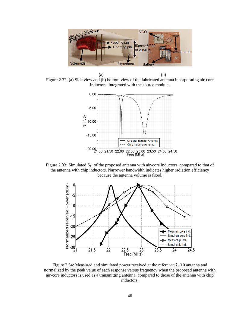
2.2.4.2. Antenna Design ...........................................................44
2.2.5. Proximity Effect of Nearby Objects ....................................48
3. Realization of Omnidirectional Radiation Pattern/Broad Bandwidth for
Low Profile Antennas on a Small Ground Plane .......................................50
3.1. Low Profile Balanced-Type Omnidirectional Antennas .....................50
3.1.1. Introduction ..........................................................................50
3.1.2. Balanced Type of ICCLMA .................................................52
3.1.3. Application of Low Profile Balanced-Type Antenna ..........54
3.2. Low-profile Omnidirectional Wideband Antenna ..............................63
3.2.1. Introduction ..........................................................................63
3.2.2. Circuit Analysis of Folded Monopole Antenna with
Capacitively Coupled Parasitic Element ..............................65
3.2.2.1. Equivalent Circuit Model of Capacitively Coupled
Parasitic Element ........................................................65
3.2.2.2. Parametric Study to Set up Design Procedure ............69
3.2.3. Antenna Design ....................................................................72
3.2.3.1. Design of Meandered Folded Monopole Antenna ......72
3.2.3.2. Design of Meandered Folded Monopole Antenna with
One Parasitic Element .................................................73
3.2.3.3. Bandwidth Enhancement Using Two Back-to-Back
Parasitic Elements .......................................................75
4. A Topology-Based Miniaturization of Circularly Polarized Patch Antennas
..........................................................................................................................80
4.1. Introduction .........................................................................................80
4.2. Miniaturization of Linearly Polarized Patch Antennas Using
Meandered Metallic Traces ................................................................82
4.2.1. Wire-Mesh Microstrip Patch Antenna .................................82
4.2.2. Accordion Topology for Size Reduction .............................84
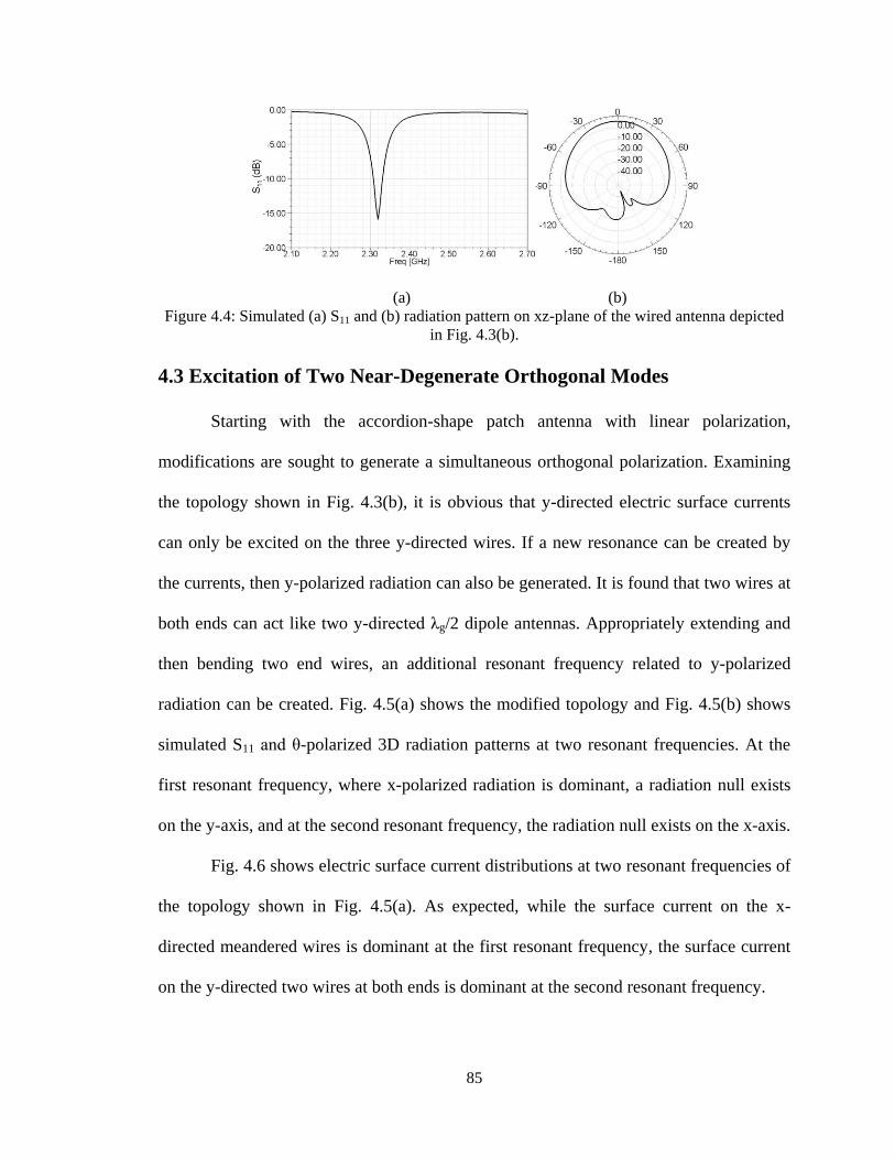
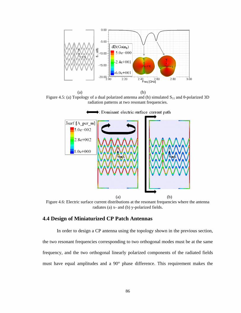
4.3. Excitation of Two Near-Degenerate Orthogonal Modes ....................85
4.4. Design of Miniaturized CP Patch Antennas .......................................86
4.5. Additional Size Reduction by Simplifying Antenna Geometry .........89
5. Design of Compact Co-Located Polarization/Pattern Diversity Antennas
Using a New Class of Microstrip Antennas .................................................95
5.1. Introduction .........................................................................................95
Page 8
vii
5.2. A New Class of Microstrip Antennas for Compact Diversity Antenna
Systems ...............................................................................................98
5.3. Compact Co-Located Diversity Antennas ........................................102
5.3.1. Design of Polarization Diversity Antenna .........................102
5.3.2. Design of Pattern Diversity Antenna .................................108
6. Conclusion and Future Work .......................................................................112
6.1. Conclusion ........................................................................................112
6.2. Suggestions for Future Work ............................................................116
6.2.1. Broadband Impedance Matching of Moderate Gain Extremely
Short Antennas ...................................................................116
6.2.2. Further Size Reduction and Bandwidth Enhancement of
Miniaturized CP Antenna Using Reactive Impedance Surface
(RIS) ...................................................................................118
6.2.3. Compact Co-Located Three-Element Diversity Antennas 119
APPENDICES ................................................................................................................121
BIBLIOGRAPHY .......................................................................................................... 131
Page 9
viii
LIST OF FIGURES
Figure
1.1 “Logjam” in communication standards due to the increasing demand for
data [1] ..................................................................................................................2
1.2 VCO module size scaling versus time [3] .............................................................3
1.3 Antenna dimensions and locations on the Samsung Galaxy S .............................3
1.4 Side views of (a) straight λ/4 monopole antenna, (b) inverted-F antenna and
(c) meandered inverted-F antenna on small ground plane ....................................6
1.5 3D radiation patterns corresponding to vertical polarization (Eθ) of (a) the
straight λ/4 monopole antenna and (b) meandered inverted-F antenna ................6
1.6 Dissertation overview ...........................................................................................8
2.1 (a) Equivalent circuit model drawn in side view and (b) top view of a
multilayer ICCLMA............................................................................................16
2.2 Design parameters of a multilayer ICCLMA ......................................................18
2.3 Equivalent circuit model of a multilayer ICCLMA ............................................20
2.4 Real and imaginary parts of input impedance simulated by full wave and
circuit simulators .................................................................................................20
2.5 Simulated S11 when L = λ0/8 and h = λ0 /40 .......................................................20
2.6 Simulated (a) E-Plane and (b) H-Plane radiation patterns when L = λ0/8 and
h = λ0/40 ..............................................................................................................21
2.7 E-Plane radiation patterns of (a) a conventional inverted-F antenna and (b)
multi-element monopole antenna with the same vertical profile as the
height of the proposed antenna (=λ0/40) .............................................................23
2.8 Topology of single-layer ICCLMA ....................................................................24
Page 10
ix
2.9 Simulated (a) E-Plane and (b) H-Plane radiation patterns of a single layer
ICCLMA when L = λ0/8 and h = λ0/40 ...............................................................24
2.10 Equivalent circuit model of single-layer ICCLMA ............................................24
2.11 Design procedure for additional size reduction of single-layer ICCLMA .........25
2.12 (a) Miniaturized single-layer ICCLMA and (b) measurement set up using a
large ground plane (3λ0 X 3λ0) ...........................................................................27
2.13 Measured and simulated S11 of a miniaturized single-layer ICCLMA on a
large ground plane ...............................................................................................27
2.14 Measured E-Plane radiation patterns of a ICCLMA and λ0/4 monopole
antenna ................................................................................................................28
2.15 (a) Two vertical elements put λ0/2 away from each other, (b) its circuit
model and (c) a circuit model for the conventional T-type 180 degree phase
shifter ..................................................................................................................31
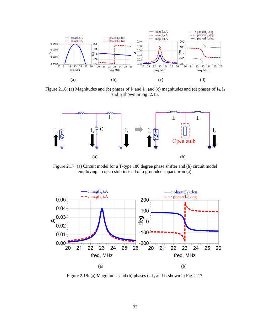
2.16 (a) Magnitudes and (b) phases of I1 and I2, and (c) magnitudes and (d)
phases of I3, I4 and I5 shown in Fig. 2.15 ............................................................32
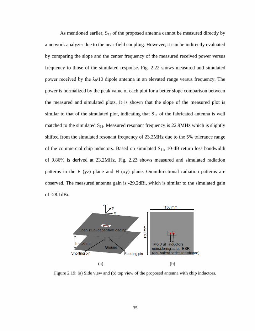
2.17 (a) Circuit model for a T-type 180 degree phase shifter and (b) circuit
model employing an open stub instead of a grounded capacitor in (a) ..............32
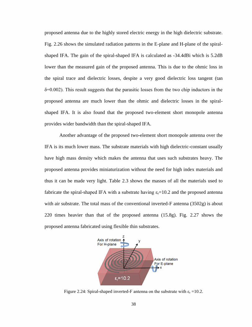
2.18 (a) Magnitudes and (b) phases of I6 and I7 shown in Fig. 2.17 ...........................32
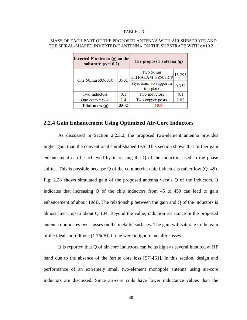
2.19 (a) Side view and (b) top view of the proposed antenna with chip inductors .....35
2.20 (a) Simulated S11 of the proposed antenna with chip inductors and (b)
measurement setup in an elevated antenna range ...............................................36
2.21 Fabricated antenna with chip inductors, integrated with the source module ......36
2.22 Measured and simulated power received at the reference λ0/10 dipole
antenna and normalized by the peak value of each response versus
frequency when the proposed antenna with chip inductors is used as a
transmitting antenna ............................................................................................36
2.23 Measured and simulated radiation patterns of the proposed antenna with
chip inductors in the (a) E (=yz) plane and (b) H (=xy) plane ............................37
2.24 Spiral-shaped inverted-F antenna on the substrate with εr =10.2 .......................38
2.25 Simulated S11 of spiral-shaped inverted-F antenna on the substrate with εr
=10.2, compared to that of the proposed antenna with chip inductors ...............39
Page 11
x
2.26 Simulated radiation patterns of spiral-shaped inverted-F antenna on the
substrate with εr =10.2 in the (a) E (=yz) plane and (b) H (=xy) plane ..............39
2.27 Proposed antenna fabricated using flexible thin substrates ................................39
2.28 Simulated gains of the proposed antennas with chip inductors versus Q of
the chip inductors ................................................................................................41
2.29 Design parameters of the air-core coil ................................................................42
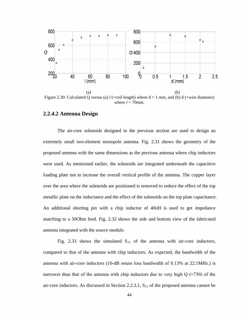
2.30 Calculated Q versus (a) l (=coil length) where d = 1mm, and (b) d (=wire
diameter) where l = 70mm ..................................................................................44
2.31 Geometry of the proposed antenna with air-core inductors having the
dimensions of 150mm X 150mm X 50mm.........................................................45
2.32 (a) Side view and (b) bottom view of the fabricated antenna incorporating
air-core inductors, integrated with the source module ........................................46
2.33 Simulated S11 of the proposed antenna with air-core inductors, compared to
that of the antenna with chip inductors. Narrower bandwidth indicates
higher radiation efficiency because the antenna volume is fixed .......................46
2.34 Measured and simulated power received at the reference λ0/10 antenna and
normalized by the peak value of each response versus frequency when the
proposed antenna with air-core inductors is used as a transmitting antenna,
compared to those of the antenna with chip inductors ........................................46
2.35 Measured and simulated radiation patterns of the proposed antenna with
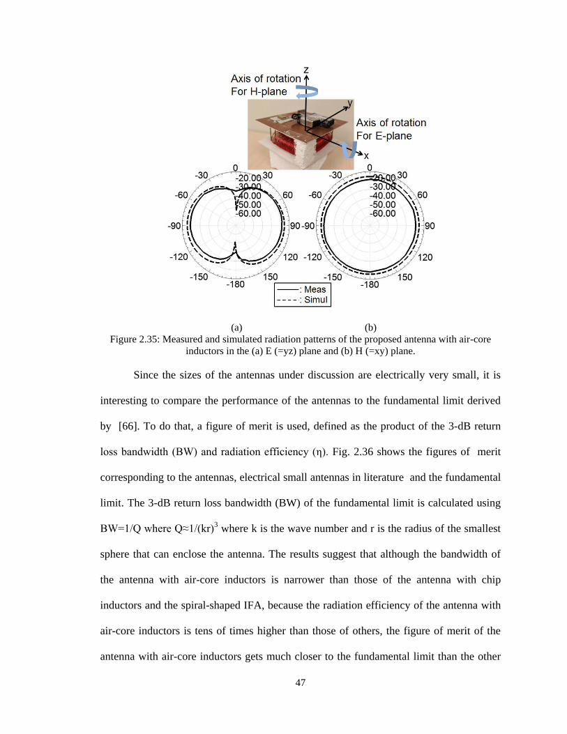
air-core inductors in the (a) E (=yz) plane and (b) H (=xy) plane ......................47
2.36 Performance comparison among the electrically small antennas shown in
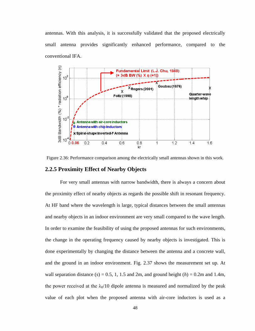
this work..............................................................................................................48
2.37 Measurement set up for examining the proximity effect of nearby objects
on the resonant frequency of the proposed narrow band antenna .......................49
2.38 Measured received normalized power corresponding to various positions of
the transmitting (=proposed) antenna shown in Fig. 2.37 ..................................49
3.1 Electric field distribution in the proposed antenna fed by coaxial cable ............51
3.2 Simulated E-Plane radiation pattern of single-layer ICCLMA (a) without
and (b) with a coaxial cable ................................................................................51
3.3 Measurement method using a balanced architecture ..........................................53
3.4 Side, top and bottom views of measurement set up of a balanced
miniaturized antenna compatible with unbalanced measurement system ..........53
Page 12
xi
3.5 Measured and simulated S11 of the proposed balanced architecture. ..................54
3.6 Measured and simulated (a) E-Plane (=XZ-Plane) and (b) H-Plane (=XY-
Plane) radiation patterns of the proposed balanced architecture ........................54
3.7 (a) Layout of Crawling Robot and (b) location and space for antenna ...............55
3.8 Integration of an embedded antenna with Bluetooth module .............................55
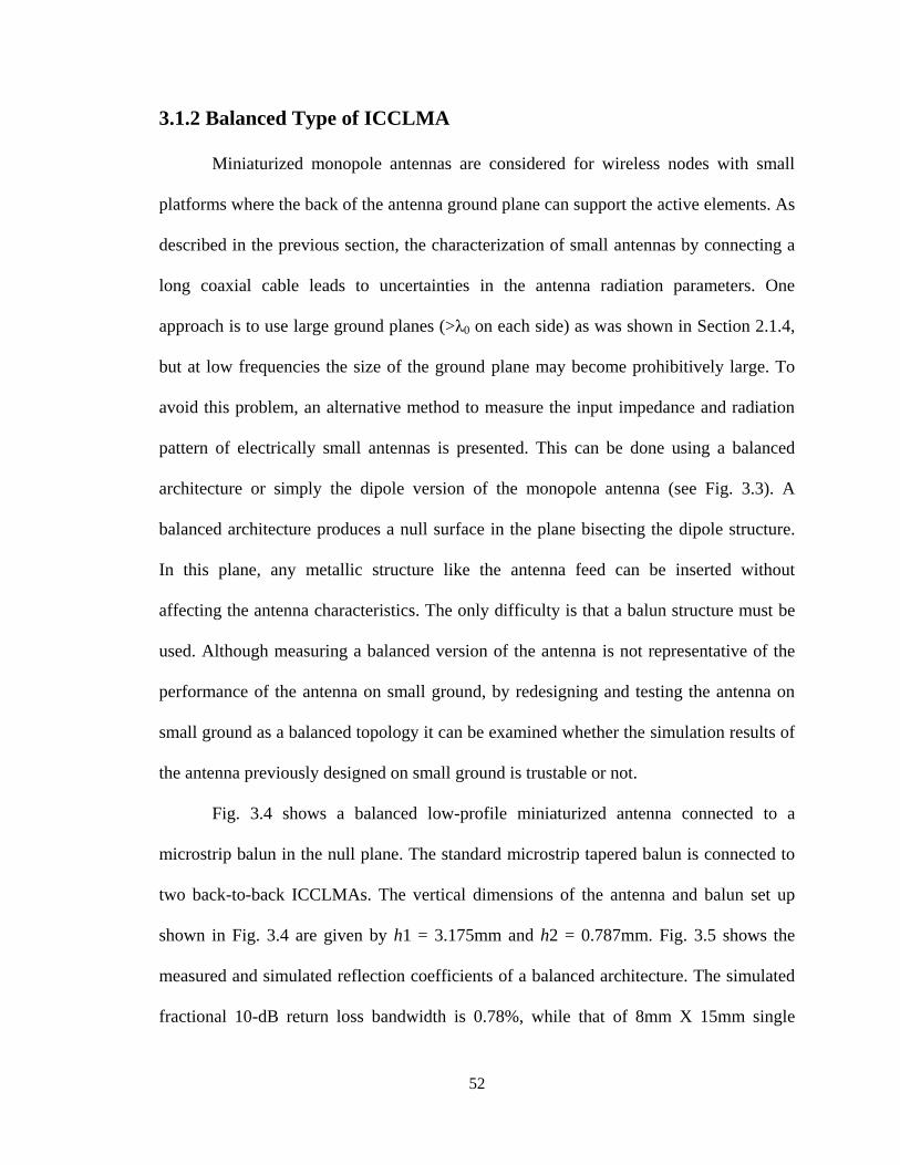
3.9 (a) Meandered monopole antenna, (b) 2D and (c) 3D radiation pattern of v-
pol .......................................................................................................................56
3.10 Suppression of radiation from horizontal current using extended ground ..........56
3.11 (a) The proposed antenna and (b) its surface current distribution ......................57
3.12 2D and 3D radiation patterns of the proposed antenna .......................................57
3.13 Embedded antenna inside paper and its 2D/3D radiation patterns .....................58
3.14 (a) Lift-off, (b) Shadow mask, and (c) Etch-back ...............................................59
3.15 (a) Photoresist laminator, (b) exposure machine, and (c) sputtering system ......59
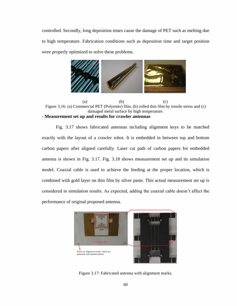
3.16 (a) Commercial PET (Polyester) film, (b) rolled thin film by tensile stress
and (c) damaged metal surface by high temperature ..........................................60
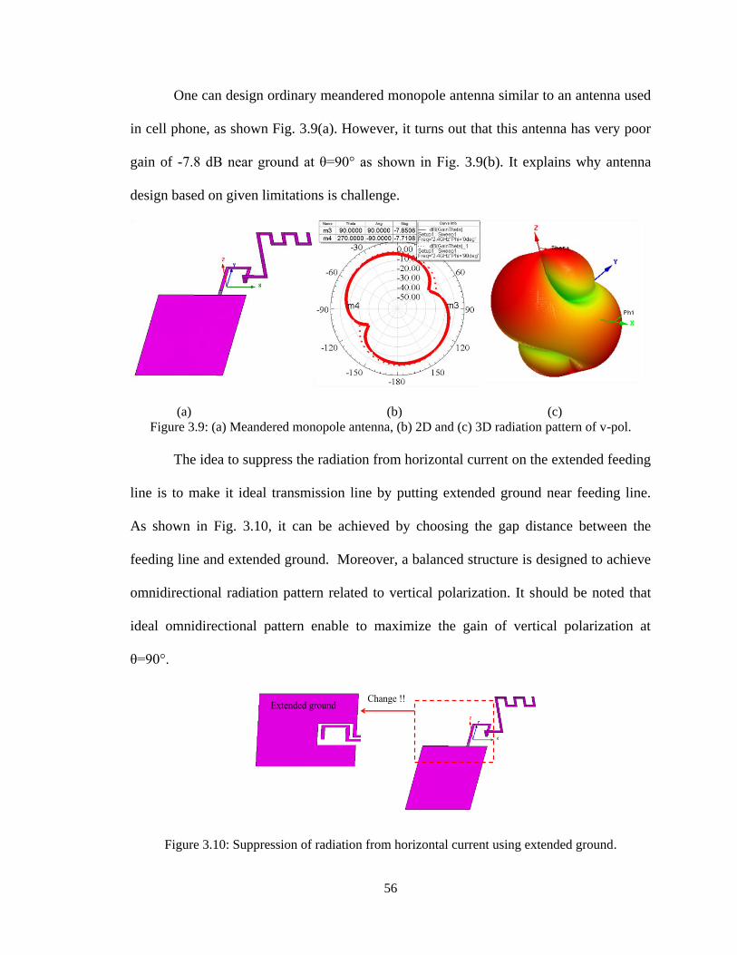
3.17 Fabricated antenna with alignment marks ..........................................................60
3.18 (a) Measurement set up and (b) its simulation model .........................................61
3.19 Measured and simulated return loss (S11) ...........................................................61
3.20 Measured (a) E-planes and (b) H-planes of λ/2 dipole and proposed
antennas...............................................................................................................62
3.21 Embedded antenna inside a crawler robot ..........................................................62
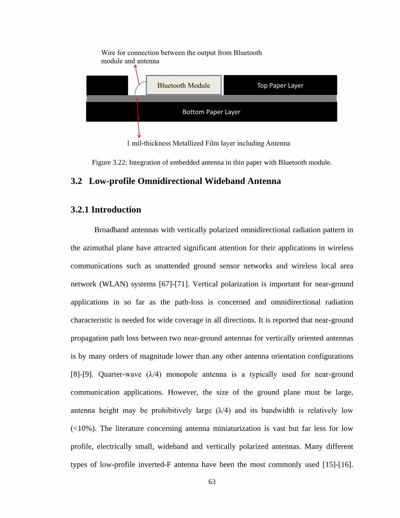
3.22 Integration of embedded antenna in thin paper with Bluetooth module .............63
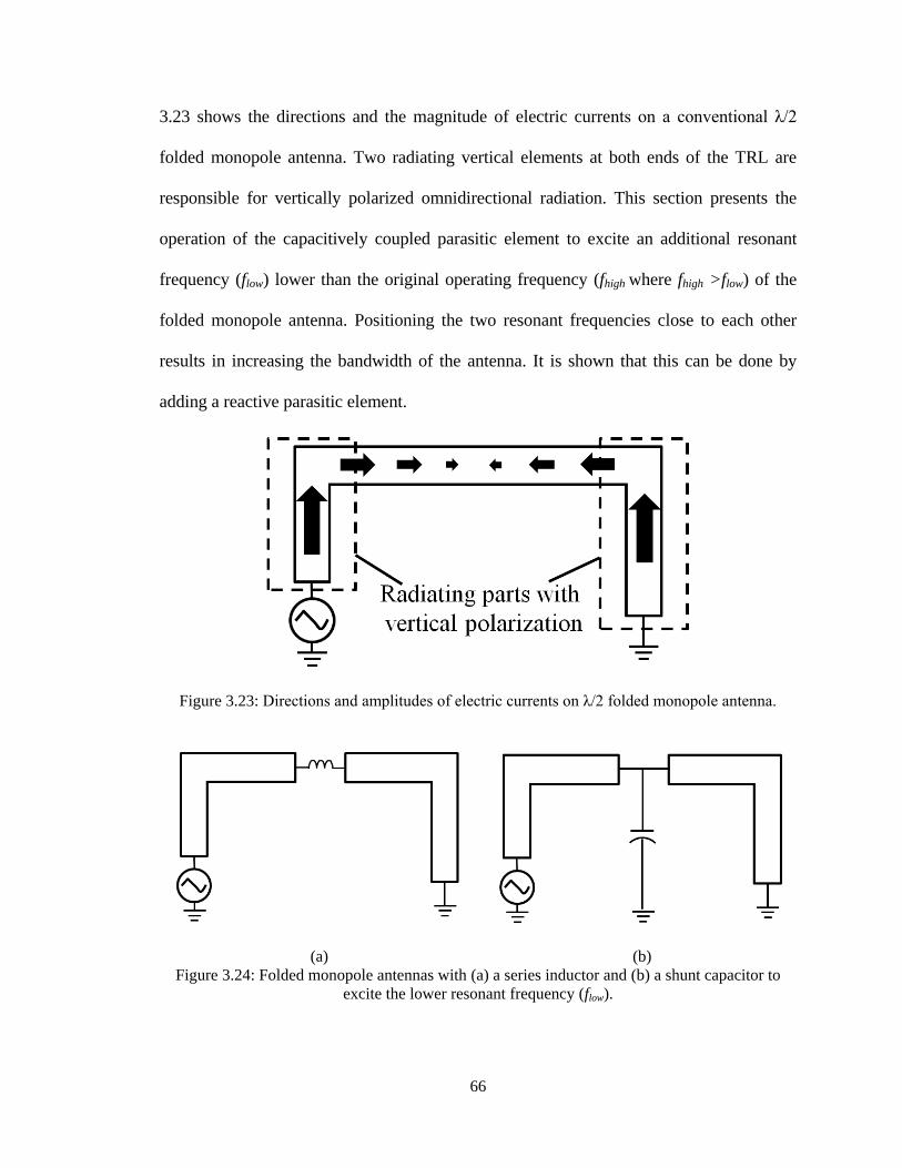
3.23 Directions and amplitudes of electric currents on λ/2 folded monopole
antenna ................................................................................................................66
3.24 Folded monopole antennas with (a) a series inductor and (b) a shunt
capacitor to excite the lower resonant frequency (flow) .......................................66
3.25 (a) Side view of λ/2 folded monopole antenna with a capacitively coupled
parasitic element and (b) equivalent circuit model of the parasitic element .......67
Page 13
xii
3.26 Imaginary part of Zin in the equivalent circuit model of the capacitively
coupled parasitic element shown in Fig. 3.25(b), compared to the same
circuit model without C1 .....................................................................................69
3.27 Input admittances toward two shorting sheets and parasitic element in the
middle of a shorted λ/2 TRL ...............................................................................70
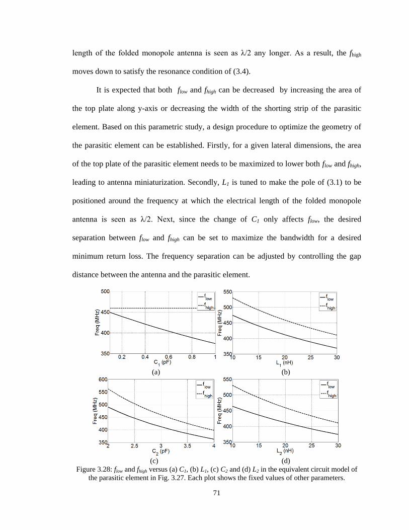
3.28 flow and fhigh versus (a) C1, (b) L1, (c) C2 and (d) L2 in the equivalent circuit
model of the parasitic element in Fig. 3.27 .........................................................71
3.29 Geometries and electric current distributions of (a) the straight and (b)
meandered λ/2 folded monopole antenna ...........................................................73
3.30 Design parameters of the meandered λ/2 folded monopole antenna ..................73
3.31 Simulated S11 as a function of Wb in Fig. 3.30 ....................................................73
3.32 Geometry and design parameters of the meandered λ/2 folded monopole
antenna with the capacitively coupled parasitic element ....................................74
3.33 Simulated S11 as a function of (a) g, (b) Ld and (c) Wd .......................................75
3.34 Geometry and design parameters of the omnidirectional antenna topology
with two back-to-back parasitic elements ...........................................................77
3.35 Simulated S11 corresponding to three cases: i. Antenna without any
parasitic element (‘no parasitic’), ii. Antenna with one parasitic element
(‘one parasitic’) and iii. Antenna with two parasitic elements (denoted by
‘two parasitic’) ....................................................................................................77
3.36 Horizontal electric current distribution at (a) 328MHz and (b) 419MHz ...........77
3.37 Measured S11 corresponding to the three cases: I. No parasitic, II. One
parasitic and III. Two parasitic ...........................................................................78
3.38 Measured radiation patterns of the proposed antenna at 310MHz: (a) E-
Plane and (b) H-Plane .........................................................................................78
3.39 Measured radiation patterns of the proposed antenna at 430MHz: (a) E-
Plane and (b) H-Plane .........................................................................................79
4.1 Conversion of a λg/2 microstrip antenna to an array of thin wires .....................83
4.2 Simulated (a) S11 and (b) radiation pattern on xz-plane of a wire mesh patch
antenna and a conventional λg/2 microstrip antenna with the same sizes and
substrate ..............................................................................................................83
4.3 (a) Shrunk wires and (b) sinusoidal wires with the elimination of wires in
parallel with y-axis ..............................................................................................84
Page 14
xiii
4.4 Simulated (a) S11 and (b) radiation pattern on xz-plane of the wired antenna
depicted in Fig. 4.3(b) .........................................................................................85
4.5 (a) Topology of a dual polarized antenna and (b) simulated S11 and θ-
polarized 3D radiation patterns at two resonant frequencies ..............................86
4.6 Electric surface current distributions at the resonant frequencies where the
antenna radiates (a) x- and (b) y-polarized fields ...............................................86
4.7 (a) Topology, design parameters and (b) simulated S11 of the proposed CP
antenna exhibiting 59% size reduction as compared to the conventional
corner-truncated square microstrip antenna ........................................................88
4.8 Simulated axial ratio in the broadside direction for the antenna shown in
Fig. 4.7(a) ............................................................................................................88
4.9 Simulated radiation patterns in two orthogonal planes of (a) xz and (b) yz-
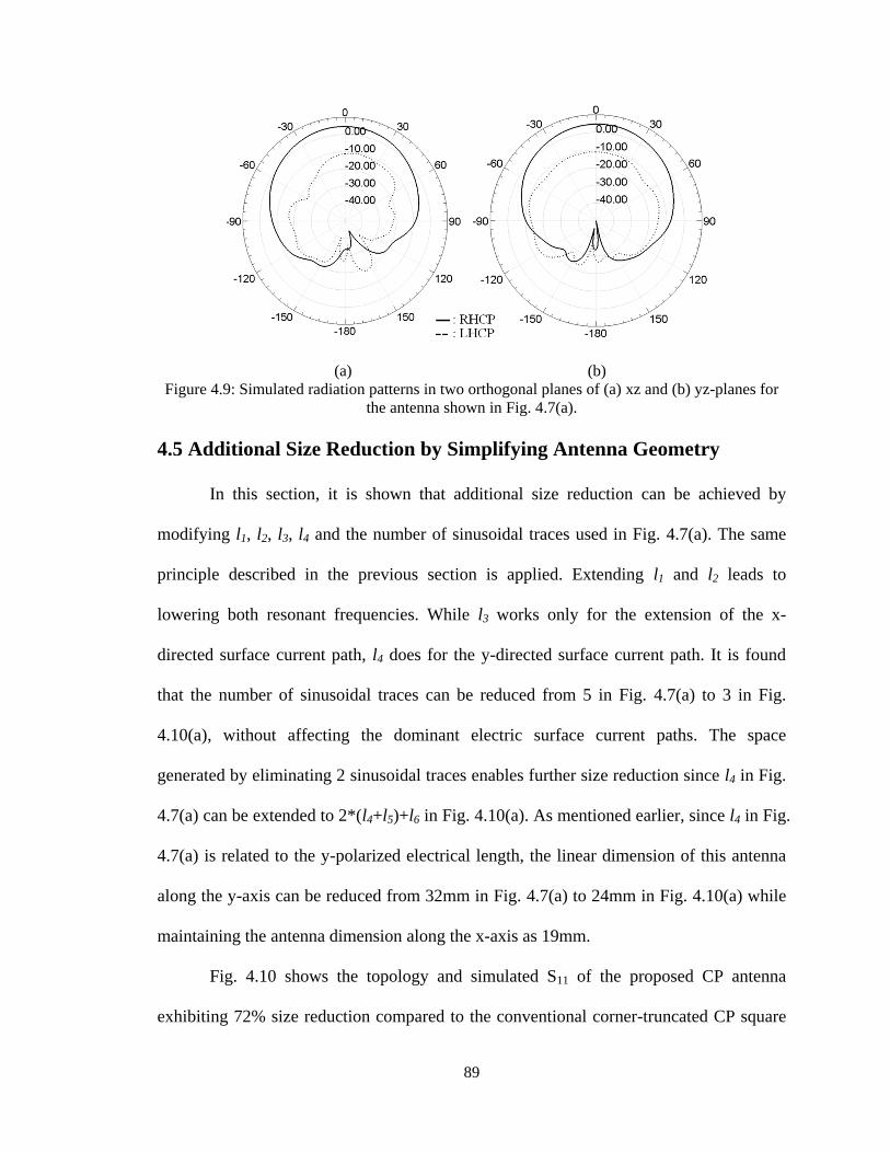
planes for the antenna shown in Fig. 4.7(a) ........................................................89
4.10 (a) Topology, design parameters and (b) simulated S11 of the proposed CP
antenna exhibiting 72% size reduction as compared to the conventional
corner-truncated square microstrip antenna ........................................................90
4.11 Simulated axial ratio in the broadside direction for the antenna shown in
Fig. 4.10(a) ..........................................................................................................90
4.12 Simulated radiation patterns in two orthogonal planes of (a) xz and (b) yz-
planes for the antenna shown in Fig. 4.10(a) ......................................................90
4.13 (a) Topology, design parameters and (b) measured S11 of the proposed CP
antenna exhibiting 53% size reduction as compared to the conventional
corner-truncated square microstrip antenna ........................................................92
4.14 Measured axial ratio in the broadside direction for the antenna shown in
Fig. 4.13(a) ..........................................................................................................92
4.15 Measured radiation patterns in two orthogonal planes of (a) xz and (b) yz-
planes for the antenna shown in Fig. 4.13(a) ......................................................93
4.16 (a) Topology, design parameters and (b) measured S11 of the proposed CP
antenna exhibiting 75% size reduction as compared to the conventional
corner-truncated square microstrip antenna ........................................................93
4.17 Measured axial ratio in the broadside direction for the antenna shown in
Fig. 4.16(a) ..........................................................................................................94
4.18 Measured radiation patterns in two orthogonal planes of (a) xz and (b) yz-
planes for the antenna shown in Fig. 4.16(a) ......................................................94
Page 15
xiv
5.1 (a) Proposed microstrip antenna with an open area in its middle and (b)
bow-tie version of the proposed microstrip antenna on the infinite ground
plane ....................................................................................................................99
5.2 Distributions of (a) voltage and (b) current on the λ/2 microstrip antenna
with x-polarized radiation on the infinite ground plane ......................................99
5.3 Geometry and design parameters of the bow-tie version of the proposed
microstrip antenna with an open area in its middle ..........................................100
5.4 Simulated S11 of the proposed bow-tie microstrip antenna shown in Fig. 5.3 ..100
5.5 Current distributions of the proposed antenna in Fig. 5.3 at (a) 342MHz and
(b) 456MHz .......................................................................................................101
5.6 Simulated radiation patterns of the proposed bow-tie microstrip antenna on
E-plane (xz-plane) at two resonant frequencies, corresponding to (a) PIFA
and (b) patch operation shown Fig. 5.4 .............................................................101
5.7 Simulated S11 of the proposed bow-tie microstrip antenna versus g1 ...............101
5.8 (a) Proposed bow-tie microstrip antenna with x-pol and (b) conventional
bow-tie microstrip antenna with y-pol ..............................................................103
5.9 Geometry and design parameters of the proposed polarization diversity
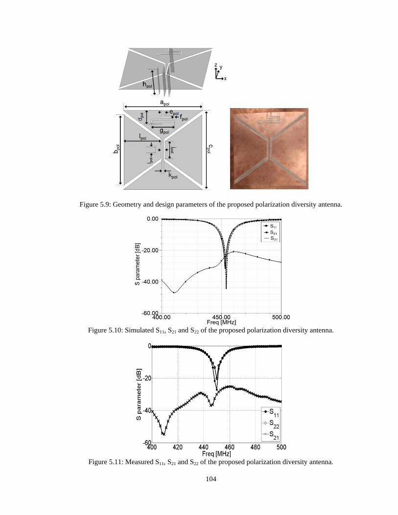
antenna ..............................................................................................................104
5.10 Simulated S11, S21 and S22 of the proposed polarization diversity antenna ......104
5.11 Measured S11, S21 and S22 of the proposed polarization diversity antenna .......104
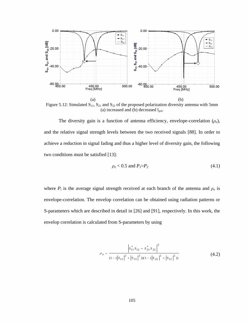
5.12 Simulated S11, S21 and S22 of the proposed polarization diversity antenna
with 5mm (a) increased and (b) decreased lpol ..................................................105
5.13 Simulated radiation efficiency of two antenna elements in the proposed
polarization diversity antenna ...........................................................................107
5.14 Envelop correlation (ρe) between radiation patterns of two antenna
elements in the proposed polarization diversity antenna and diversity gain ....107
5.15 Measured radiation patterns on E-planes of two bow-tie microstrip
antennas: (a) Port1: ON and Port2: OFF (50Ω terminated) and (b) Port1:
OFF (50Ω terminated) and Port2: ON ..............................................................107
Page 16
xv
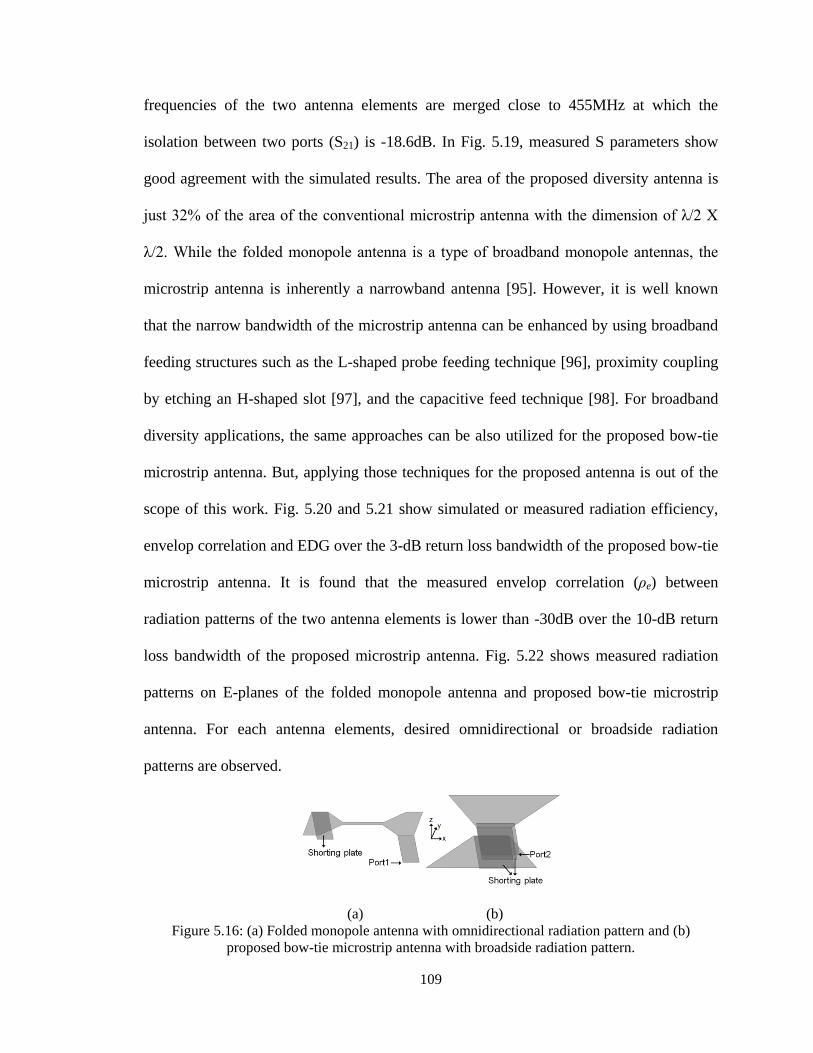
5.16 (a) Folded monopole antenna with omnidirectional radiation pattern and (b)
proposed bow-tie microstrip antenna with broadside radiation pattern ............109
5.17 Geometry and design parameters of the proposed pattern diversity antenna ...110
5.18 Simulated S11, S21 and S22 of the proposed pattern diversity antenna ..............110
5.19 Measured S11, S21 and S22 of the proposed pattern diversity antenna ...............110
5.20 Simulated radiation efficiency of two antenna elements in the proposed
pattern diversity antenna ...................................................................................111
5.21 Envelop correlation (ρe) between radiation patterns of two antenna
elements in the proposed pattern diversity antenna and diversity gain ............111
5.22 Measured radiation patterns on E-planes of the folded monopole antenna
and proposed bow-tie microstrip antenna: (a) Port1: ON and Port2: OFF
(50Ω terminated) and (b) Port1: OFF (50Ω terminated) and Port2: ON ..........111
6.1 Antenna gain with and without considering impedance mismatch factor to a
feed (ηimf) ...........................................................................................................117
6.2 Extremely short monopole antenna connected in series with a negative
capacitor ............................................................................................................117
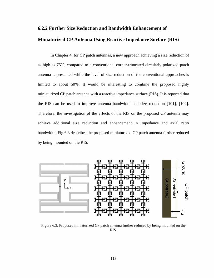
6.3 Proposed miniaturized CP patch antenna further reduced by being mounted
on the RIS .........................................................................................................118
6.4 S11 and electric surface current distributions at two modes of the proposed
microstrip antenna .............................................................................................120
6.5 Expected (a) topology of the 3-element diversity antenna and (b) S11, S22
and S33 ...............................................................................................................120
A.1 Radiation pattern diversities using two antennas ..............................................122
A.2 Indoor scenario utilizing radiation pattern diversity antenna system ...............123
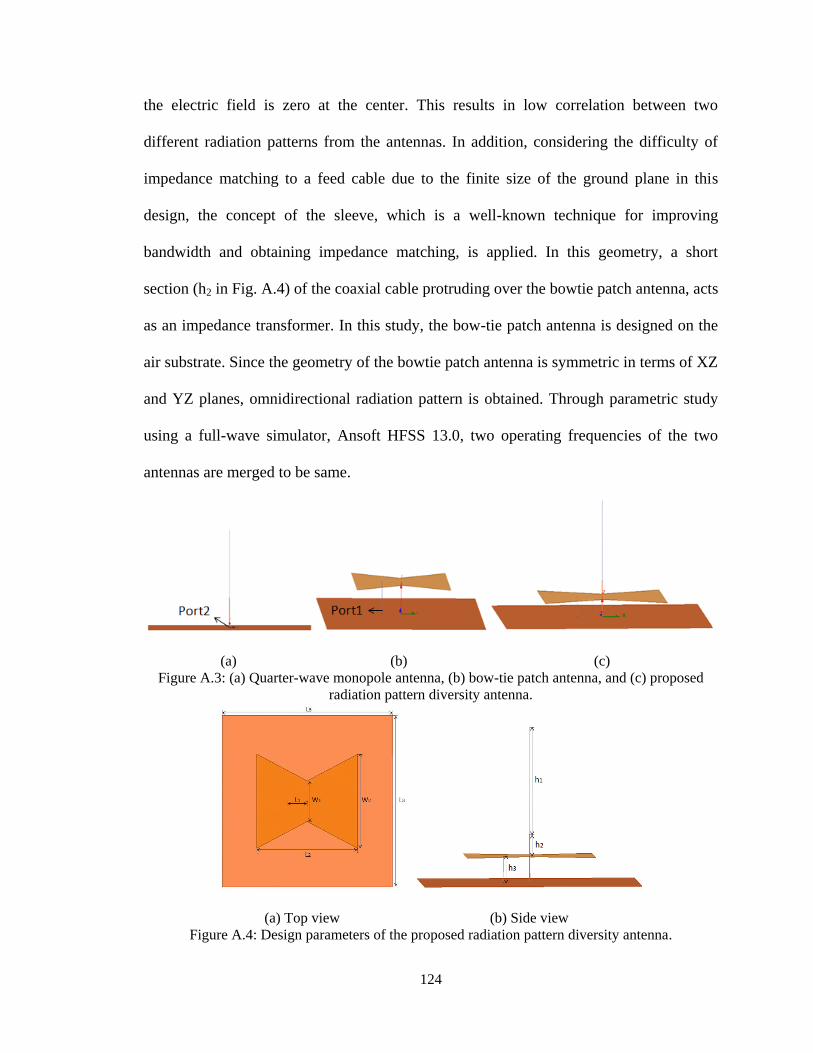
A.3 (a) Bow-tie patch antenna, (b) bow-tie patch antenna, and (c) proposed
radiation pattern diversity antenna ....................................................................124
A.4 Design parameters of the proposed radiation pattern diversity antenna ...........124
A.5 Simulated S parameters of the proposed radiation pattern diversity antenna ...125
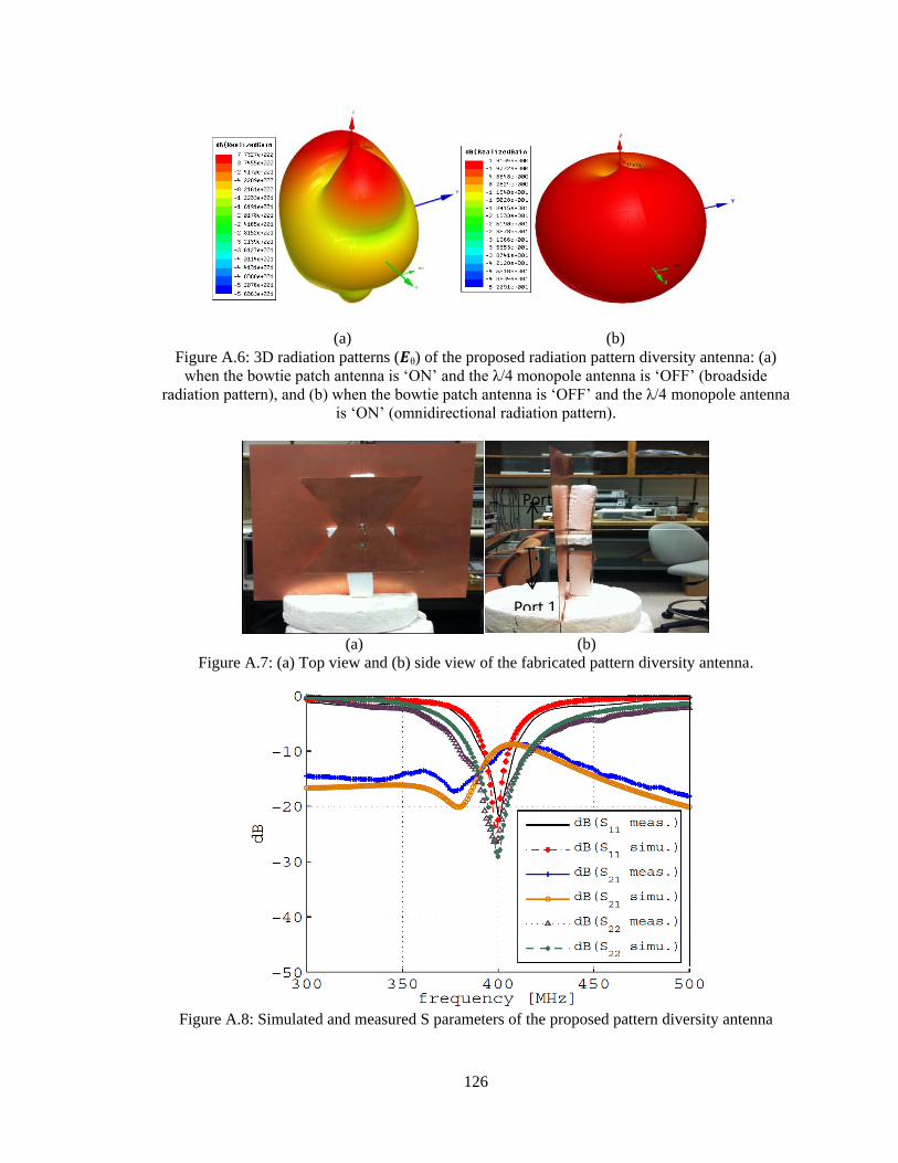
A.6 3D radiation patterns (𝑬θ) of the proposed radiation pattern diversity
antenna: (a) when the bowtie patch antenna is ‘ON’ and the λ/4 monopole
antenna is ‘OFF’ (broadside radiation pattern), and (b) when the bowtie
Page 17
xvi
patch antenna is ‘OFF’ and the λ/4 monopole antenna is ‘ON’
(omnidirectional radiation pattern) ...................................................................126
A.7 (a) Top view and (b) side view of the fabricated pattern diversity antenna .....126
A.8 Simulated and measured S parameters of the proposed pattern diversity
antenna ..............................................................................................................126
A.9 Schematics of (a) the transmitter and (b) receiver utilizing the proposed
diversity antennas ..............................................................................................128
A.10 (a) Fabricated diversity antennas and (b) receiving module .............................128
A.11 Received system including diversity antennas and a computer ........................128
A.12 Measurement set up on 3rd floor in EECS building in the University of
Michigan ...........................................................................................................129
A.13 Two output signals from the two receiving antennas (a) when monopole
antenna is ‘ON’ and patch antenna is ‘OFF’ and (b) when monopole
antenna is ‘OFF’ and patch antenna is ‘ON’ .................................................... 130
Page 18
xvii
LIST OF TABLES
Table
2.1 GAIN AND DIMENSION OF A CONVENTIONAL INVERTED-F
ANTENNA, MMA AND PROPOSED ANTENNA ..........................................22
2.2 GAIN AND RESONANT FREQUENCY OF SINGLE-LAYER ICCLMAS
WITH THREE DIFFERENT DIMENSIONS ....................................................26
2.3 MASS OF EACH PART OF THE PROPOSED ANTENNA WITH AIR
SUBSTRATE AND THE SPIRAL-SHAPED INVERTED-F ANTENNA ON
THE SUBSTRATE WITH εr=10.2 .....................................................................40
4.1 MEASUREMENT RESULTS OF THE PROPOSED ANTENNAS IN FIG.
4.13(A) AND 4.16(A) ......................................................................................... 94
Page 19
xviii
LIST OF APPENDICES
Appendix
A. Pattern Diversity Antenna System .............................................................. 121
Page 20
xix
ABSTRACT
Advanced Antenna Miniaturization Techniques for Low-
Power, Broadband and Diversity Wireless Systems
by
Jungsuek Oh
Chair: Kamal Sarabandi
Nowadays miniaturized low-power electronics and wireless devices are
ubiquitous in everyday life. However, there is still significant interest to further reduce
size, lower the power and improve data rate required by such systems. For such goals,
antennas still constitute a major bottleneck in terms of size, efficiency, polarization and
radiation pattern. Also for many near ground applications, low profile small antennas
with vertical polarization are needed to achieve much lower propagation path loss.
Conventional approaches to reduce the height of monopole antennas cause
significant drop in efficiency and polarization purity. Two novel miniaturization
techniques are presented for different levels of size reduction (λ/300 < h < λ/45 where h
is antenna height). For h ≈ λ/45, a novel inductively coupled capacitively loaded antenna
topology is presented, which enables up to 9dB higher gain than the conventional
Page 21
xx
inverted-F antenna with a small ground plane. For extremely short monopole antennas
with h ≈ λ/300, an in-phase two-element monopole antenna topology is demonstrated,
which exhibits 16.5 dB higher gain than the conventional inverted-F antenna having the
same dimensions. Also, radiation pattern deformation caused by low profile
configurations on a small ground plane is addressed and, to solve this problem, novel
designs using vertically and horizontally balanced architectures are introduced. For GPS
or mobile platforms where the aforementioned miniaturized antennas with vertical
polarization cannot provide reliable communication connectivity, a new miniaturization
technique is presented to reduce the size of circularly polarized (CP) patch antennas. 75%
size reduction is achieved compared to a conventional patch antenna and it is 25%
smaller than the smallest CP patch antenna reported in the literature. Lastly, a novel
approach to combine the miniaturized monopole and patch antenna elements into a
compact common aperture diversity antenna is presented for MIMO applications. This
achieves a compact size of 0.27λ X 0.27λ X 0.09λ and low envelop correlation (<-30dB)
between radiation patterns of two antenna elements composing the diversity antenna.
Page 22
1
Chapter 1
Introduction
1.1 Motivation
With the great evolution of wireless technologies, the range of wireless
applications and communications standards continue to grow at an unprecedented pace
[1], [2]. Fig 1.1 shows a significant increase in the number of the communication
standards resulting from the increasing demand for data. This requires highly integrated
and power efficient RF front-ends to achieve wireless connectivity in ever-smaller and
battery sensitive mobile devices. In order to satisfy the demanding space constraints
imposed by the wireless devices, the volume of active circuit elements has been
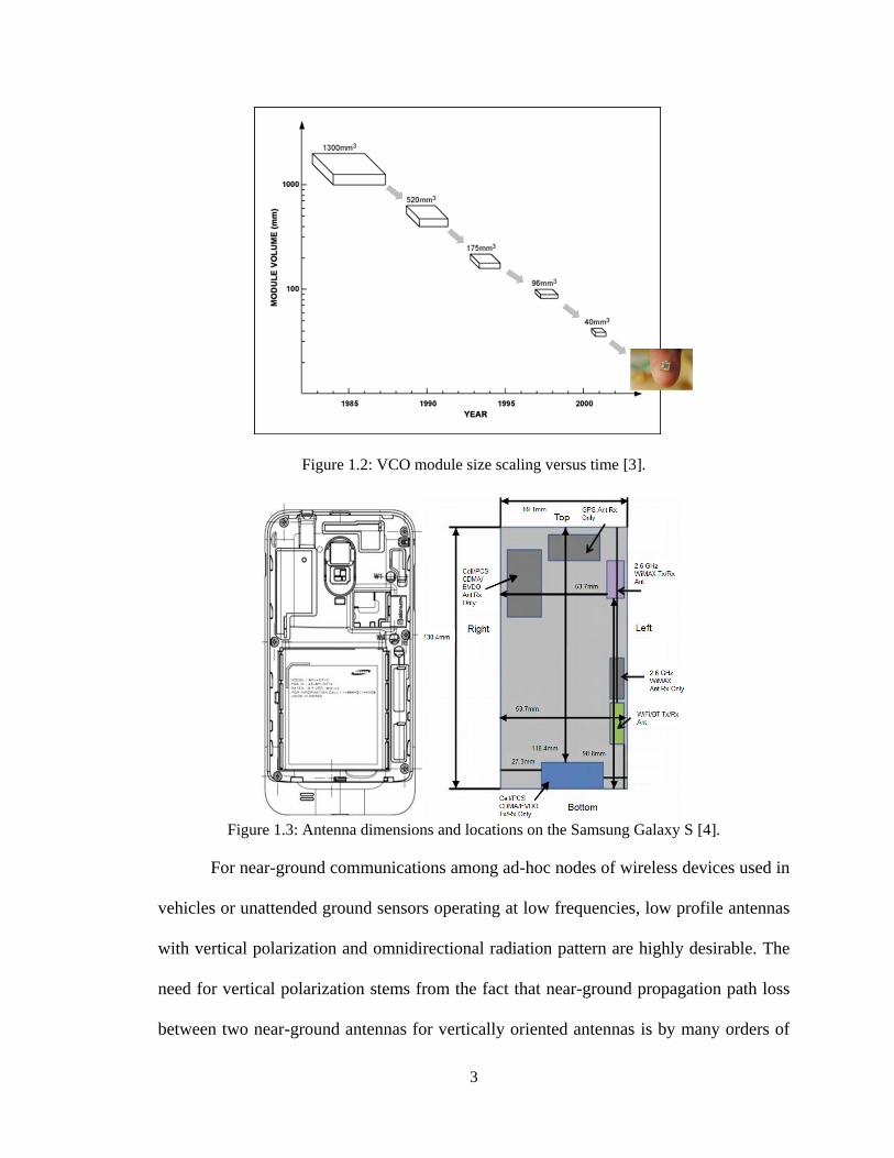
amazingly reduced. Fig. 1.2 illustrates the size reduction over time of the "typical" state-
of-the-art commercial voltage controlled oscillator (VCO) module [3]. For the most
recent 10 years, the size is reduced by a factor of 10 with enhanced performance. On the
other hand, although there have been significant efforts towards antenna miniaturization,
the antennas integrated with such active elements are still bulky and have a low
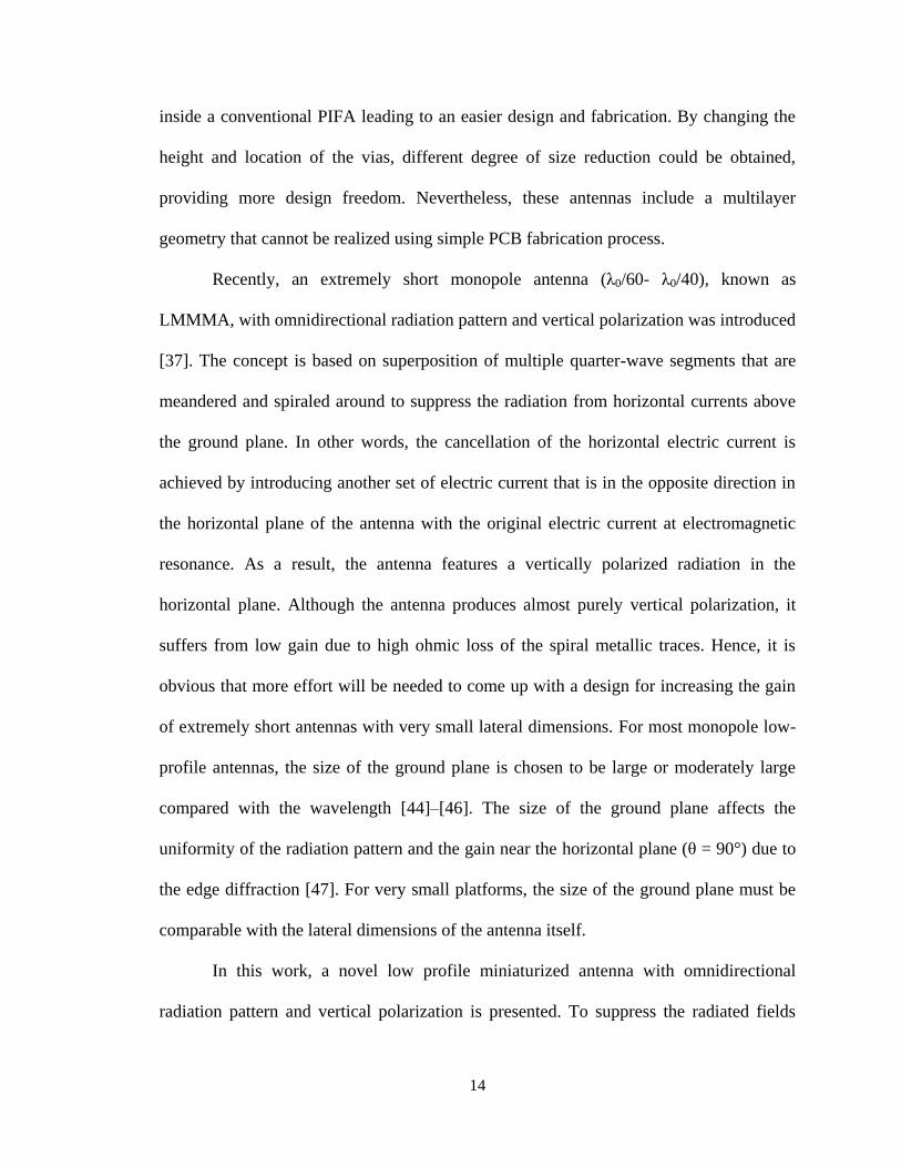
efficiency. Fig 1.3 shows antenna dimensions and locations on the Samsung Galaxy S [4].
This suggests that the antennas occupy almost the whole volume of RF modules.
Furthermore, for recent low-frequency wireless applications such as ground and
Page 23
2
biomedical sensor networks, design of efficient antennas with small form factor is getting
more challenging [5]–[7]. In radio wave propagation, selecting operating frequencies of
wireless systems as low as possible can mitigate signal attenuation and fading effects
significantly because at lower frequency, the distance between a transmitter and receiver
and the size of scatterers look effectively much smaller, which results in better wave
penetration through obstacles. However, under the fixed physical volume, design of
electrically smaller antennas using conventional approaches causes significant drops in
bandwidth, radiation efficiency and polarization purity, and deformation in radiation
pattern. Therefore, this dissertation focuses on the study of novel antenna miniaturization
techniques considering the aforementioned performance parameters.
Figure 1.1: “Logjam” in communication standards due to the increasing demand for data [1].
Page 24
3
Figure 1.2: VCO module size scaling versus time [3].
Figure 1.3: Antenna dimensions and locations on the Samsung Galaxy S [4].
For near-ground communications among ad-hoc nodes of wireless devices used in
vehicles or unattended ground sensors operating at low frequencies, low profile antennas
with vertical polarization and omnidirectional radiation pattern are highly desirable. The
need for vertical polarization stems from the fact that near-ground propagation path loss
between two near-ground antennas for vertically oriented antennas is by many orders of
Page 25
4
magnitude lower than any other antenna orientation configurations [8]-[10]. The
omnidirectional radiation characteristic is needed for wide coverage in all directions. For
applications where the orientation of transmitting or receiving antennas may vary, such as
mobile platforms and GPS, circularly polarized (CP) antennas are desirable because CP
can maximize the polarization efficiency and improve the propagation link budget for
such wireless platforms [11]. Considering that most miniaturization techniques are
developed for linearly polarized antennas, a new approach to further reduce the size of
the CP patch antennas is needed. Lastly, in the next generation of mobile communication
systems there is a stringent demand for high speed and high quality data transmission of
the mobile terminals. This makes Multiple-Input Multiple-Output (MIMO) technology
attractive for its excellent performance in channel capacity without occupying extra
spectrum and radiating power [12]. In the MIMO systems, antenna diversity is a well-
known technique to enhance the performance of wireless communication systems by
reducing the multipath fading and co-channel interference [13], [14]. Large volume that
antennas in such diversity systems occupy remains a critical problem in implementing
small wireless platforms.
1.2 Current State of the Art
In the studies regarding low profile monopole antennas with vertically
polarization, the antennas are usually loaded with horizontal resonant structures. Inverted
L and Inverted F antennas are the examples of the folded-type resonant loading structures
that are commonly used [15], [16]. However, in most of such antenna topologies with a
small ground plane, only a short vertical segment of the resonant structure contributes to
Page 26
5
the vertically polarized radiation, while the much larger portion of the antenna structure
generates higher radiation with undesired polarizations. This causes a low polarization
purity and serious deformation in the desired omnidirectional radiation pattern [17]. Fig.
1.4 and 1.5 illustrates these problems. Fig 1.4 shows side views of 1. Straight λ/4
monopole antenna, 2. Inverted-F antenna and 3. Meandered inverted-F antenna on the
small ground plane. When quarter-wave (λ/4) monopole antenna is folded to be a low
profile shape, a main beam direction is changed, as shown in Fig. 1.4(b), leading to the
decrease of antenna gain in the azimuthal (H) plane. It should be noted that with an
infinite ground plane, this doesn’t occur due to ideal images of electric currents on the
horizontal resonant structures. In addition, a meandering shape used to reduce the lateral
(horizontal) dimensions of the low profile antenna causes tailoring the electric current
path, leading to serious deterioration in polarization purity, as shown Fig. 1.4 (c). Also,
the meandered inverted-F antenna suffers from low efficiency due to high ohmic and
proximity losses from thin metallic traces. Fig 1.5 shows 3D radiation patterns
corresponding to vertical polarization (Eθ) of the straight λ/4 monopole antenna and
meandered inverted-F antenna. This suggests that in the azimuthal plane (H-plane) the
gain of the miniaturized antennas on the small ground plane can be 10dB lower than that
of the original λ/4 monopole antenna. In [18]–[23], interesting capacitively loaded
monopole antennas with different especial disk geometries are presented as means for
reducing the antenna height and improving the bandwidth. The heights of these antennas
are in the range of λ/10, presenting excellent operational bandwidth. However, their
lateral dimensions are still large, comparable to the wavelength.
Page 27
6
(a) (b) (c)
Figure 1.4: Side views of (a) straight λ/4 monopole antenna, (b) inverted-F antenna and (c)
meandered inverted-F antenna on small ground plane.
(a) (b)
Figure 1.5: 3D radiation patterns corresponding to vertical polarization (Eθ) of (a) the straight λ/4
monopole antenna and (b) meandered inverted-F antenna.
For GPS or mobile platforms where the aforementioned low profile antennas with
vertical polarization cannot provide reliable communication connectivity, a circularly
polarized (CP) antenna with a low profile, small size and light weight is highly desirable.
However, antennas with extremely small lateral dimensions have very low capability in
internally generating the required conditions for CP operations: 1. Two orthogonal
linearly polarized components of the radiated fields, 2. Equal amplitude and a 90° phase
difference of the two components and 3. Impedance matching to a 50 ohm feed at the two
degenerate orthogonal modes. Many compact CP patch antennas have been proposed
and investigated [24]–[25]. These efforts have relied mainly on intuitive techniques such
Page 28
7
as inserting several slots or slits in suitable locations on the patch itself. In such antenna
designs, the splitting of two near-degenerate orthogonal modes with equal amplitudes and
a 90° phase difference is achieved by slightly adjusting the embedded slots, such as a
cross-slot in a patch or slits at the boundary of the patch. Theses inserted slots and slits
force redirection of the excited fundamental mode surface current and also cause the
resonant frequency to be shifted down to some extent. However, this approach has
yielded somewhat limited miniaturization due to lack of ability to simultaneously control
the surface current paths as well as create the required 90° phase difference. It is shown
that these methods can provide size reductions of as low as 50%.
For MIMO applications requiring high data rate, compact diversity antennas
composed of miniaturized low profile monopole and patch antenna elements are desirable.
In [26]–[28], the reductions in antenna size have been achieved for individual antenna
elements. However, compact diversity antennas have not been well studied. The current
approach to achieve antenna diversity is based on placing two or more individual
compact antennas in optimized positions that provide low envelope correlation (ρe) where
the envelope correlation is defined by a correlation between radiation patterns of two
individual antenna elements [26]. This approach is good but the overall volume that the
antennas occupy increases directly with their number and becomes too large for compact
wireless applications.
The focus of this thesis is to address the limitations of these current approaches by
introducing new approaches with novel antenna topologies to achieve high radiation
efficiency, high polarization purity, omnidirectional radiation pattern with small ground
plane, low envelope correlation between two miniaturized antennas, maintaining a small
Page 29
8
form factor. The novelties of the proposed antenna miniaturization techniques are
demonstrated by comparing the performance of the proposed miniaturized antennas with
that of the conventional miniaturized antennas. The proposed antenna miniaturization
techniques in this dissertation contribute to designing novel antenna topologies and RF
systems, which are introduced in IEEE Antennas and Propagation Society [17], [29]-[36].
1.3 Dissertation Overview
Figure 1.6: Dissertation overview.
1.3.1 Chapter 2: Design of Electrically Short Monopole Antenna with
High Efficiency and High Polarization Purity
Techniques are introduced to improve radiation efficiency and polarization purity
of electrically short monopole antennas. The first technique is to embed the additional
Page 30
9
coupled structure into the conventional planar inverted F antennas (PIFA) to suppress the
level of the electric surface currents with undesired polarizations. The first technique is
successfully applied for the short monopole antennas with the height of λ/45 and lateral
dimensions of λ/16 X λ/8. This antenna is called by “Low Profile Inductively Coupled
Capacitively Loaded Antenna”. However, it is found that for extremely small monopole
antennas with the height of less than λ/100 the first technique is not available and thus a
new technique utilizing two in-phase radiating elements and a low-loss phase shifter is
proposed. In order to minimize the loss of the phase shifter, a novel use of air-core
solenoids is introduced. The dimensions of the short monopole antenna designed based
on the approach are extremely small as λ/300 X λ/100 X λ/100.
1.3.2 Chapter 3: Realization of Omnidirectional Radiation
Pattern/Broad Bandwidth for Low Profile Antennas on a Small Ground
Plane
Techniques are presented to realize omnidirectional radiation pattern for the low
profile antenna on a small ground plane (<<λ). It is shown that the radiation pattern of
conventional inverted F antenna on small ground plane is distorted and as a result, the
radiated power along the azimuthal plane (H-plane) of the antenna is significantly
decreased.
The first approach to solve this problem is to utilize a balanced architecture in the
middle of which a null plane exists similar to the geometry of dipole antennas. The
second approach is to cancel out the radiated fields with undesired polarization by
manipulating the geometry of top plate of low profile antennas. In addition, a
Page 31
10
broadbanding technique compatible with the aforementioned miniaturization techniques
for realizing omnidirectional radiation pattern is presented.
1.3.3 Chapter 4: A Topology-Based Miniaturization of Circularly
Polarized Patch Antennas
A novel approach for the miniaturization of circularly polarized patch antennas is
presented. This enables a size reduction of as high as 75%, compared to a conventional
corner-truncated circularly polarized patch antenna. The proposed design procedure
consists of a number of intermediate steps, each of which produces antenna
miniaturization as well as the desired polarization and impedance matching properties.
This is very challenging in miniaturizing circularly polarized probe-fed patch antennas.
At the initial design step, a patch antenna topology made of an anisotropic conductor that
only supports the desired electric current distribution, is considered. The anisotropic
conductivity is achieved by 1) replacing the metallic patch with a set of thin parallel wire
grids aligned in the direction of the desired electric current and 2) connecting them with
two perpendicular metallic strips at each end. Next, the straight metallic traces are
meandered for size reduction, creating a miniaturized linearly polarized patch antenna.
To achieve circular polarization, a second mode is excited by elongating the end strips so
that they resonate at the same frequency. Also, the feed point is chosen so as to achieve
impedance matching and a 90° phase shift. It is shown that two resonant frequencies can
be tuned independently to produce a dual band antenna with two orthogonal polarizations.
Finally, two circularly polarized miniaturized patch antennas with different
miniaturization factors are fabricated, and their input impedances, radiation patterns and
axial ratios are discussed.
Page 32
11
1.3.4 Chapter 5: Design of Compact Co-Located Polarization/Pattern
Diversity Antennas Using a New Class of Microstrip Antennas
Compact co-located planar polarization/pattern diversity antennas using a new
class of microstrip antennas are presented. The proposed microstrip antenna has an open
area in its middle, physically splitting a single body of the conventional microstrip
antenna into two. The two bodies are magnetically coupled through two vertical shorting
plates each of which is connected to each body. A great advantage of this antenna
topology is that another antenna element can be placed in the open area, achieving the
design of compact diversity antennas with low envelop correlation. Topologies of
polarization and pattern diversity antennas incorporating the proposed microstrip antenna
and another antenna placed in the open area are introduced. Although the proposed
diversity antennas consists of two antenna elements with different polarizations or
radiation patterns, their areas are just about 30% of the area of the conventional
microstrip antenna with the dimension of λ/2 X λ/2. In addition, for both types of the
proposed diversity antennas, the envelop correlations between radiation patterns of the
two antenna elements composing each diversity antenna are lower than -30dB over the
10-dB return loss bandwidth of the proposed microstrip antenna.
Page 33
12
Chapter 2
Design of Electrically Short Monopole Antenna with High
Efficiency and High Polarization Purity
In this chapter, depending on desired levels of size reduction, two miniaturization
techniques to achieve high efficiency and polarization purity are presented: 1. Inductively
coupled capacitively loaded structure (h≈λ/45 where h is antenna height) and 2. Two in-
phase radiating elements realized by high-Q phase shifter (h≈λ/300).
2.1 Low Profile, Miniaturized, Inductively Coupled Capacitively
Loaded Monopole Antenna
2.1.1 Introduction
Vertically polarized antennas with omnidirectional radiation pattern are highly
desirable for many applications including near-ground communications among ad-hoc
nodes of wireless devices used in vehicles or unattended ground sensors operating at low
frequencies. The need for vertical polarization stems from the fact that near-ground
propagation path loss between two near-ground antennas for vertically oriented antennas
is by many orders of magnitude lower than any other antenna orientation configurations
[8], [9]. In fact, this is the main reason λ0/4 monopole antennas with vertical
Page 34
13
polarization and omnidirectional radiation pattern are prevalent in many communication
devices working near the ground. However, as wireless communication devices continue
to evolve, the large dimension of the antenna is frequently problematic. Therefore, it is
imperative to further investigate methods of realizing extremely short monopole antennas
with very small lateral dimensions, while maintaining high radiation efficiency. This will
allow ease of integration of such antennas with the package or platform of small wireless
devices that are emerging. Recently, different types of low-profile antennas with
omnidirectional radiation pattern have been proposed. Among these, one approach is to
excite radiation from short segments of loaded vertical wires, and the other one is based
on exciting a cavity-backed small slot loop antenna [38], [39].
In the studies where short segments of vertical wires are utilized as the intended
radiators, the antennas are usually loaded with horizontal resonant structures. Inverted L
and Inverted F antennas are the examples of the folded-type resonant loading structures
that are commonly used [15], [16]. One drawback of these structures is the energy
radiation in the horizontal polarization that stems from relatively large lateral dimension
of the loading structures. This, of course, leads to lower gain in the desired polarization
channel. In [18]–[23], interesting capacitively loaded monopole antennas with different
especial disk geometries are presented as means for reducing the antenna height and
improving the bandwidth. The heights of these antennas are in the range of λ0/10,
presenting excellent operational bandwidth. However, their lateral dimensions are still
comparable to the wavelength. For certain applications where the bandwidth can be
compromised, it is found that by loading the planar inverted-F antenna (PIFA), the lateral
dimension of the antenna can be reduced to λ0/8 [40]-[42]. In [42], a via-patch is added
Page 35
14
inside a conventional PIFA leading to an easier design and fabrication. By changing the
height and location of the vias, different degree of size reduction could be obtained,
providing more design freedom. Nevertheless, these antennas include a multilayer
geometry that cannot be realized using simple PCB fabrication process.
Recently, an extremely short monopole antenna (λ0/60- λ0/40), known as
LMMMA, with omnidirectional radiation pattern and vertical polarization was introduced
[37]. The concept is based on superposition of multiple quarter-wave segments that are
meandered and spiraled around to suppress the radiation from horizontal currents above
the ground plane. In other words, the cancellation of the horizontal electric current is
achieved by introducing another set of electric current that is in the opposite direction in
the horizontal plane of the antenna with the original electric current at electromagnetic
resonance. As a result, the antenna features a vertically polarized radiation in the
horizontal plane. Although the antenna produces almost purely vertical polarization, it
suffers from low gain due to high ohmic loss of the spiral metallic traces. Hence, it is
obvious that more effort will be needed to come up with a design for increasing the gain
of extremely short antennas with very small lateral dimensions. For most monopole low-
profile antennas, the size of the ground plane is chosen to be large or moderately large
compared with the wavelength [44]–[46]. The size of the ground plane affects the
uniformity of the radiation pattern and the gain near the horizontal plane (θ = 90°) due to
the edge diffraction [47]. For very small platforms, the size of the ground plane must be
comparable with the lateral dimensions of the antenna itself.
In this work, a novel low profile miniaturized antenna with omnidirectional
radiation pattern and vertical polarization is presented. To suppress the radiated fields
Page 36
15
from horizontal currents over a top load the horizontal currents are distributed uniformly
over a large metallic top load. However, the use of this large top load in miniaturized
antennas prohibits the use of thin shorting pins because impedance matching to 50 ohm
cannot be obtained without the increase in the dimension of the shorting pins. In the
proposed antenna, a new in-plane capacitive coupled structure is introduced for
compensating inductive coupling between the thin pins. Finally, the use of the large top
load, shorting pin and in-plane capacitive coupled structure achieve improved
polarization purity and excellent impedance matching with antenna miniaturization. An
equivalent circuit model of the proposed antenna is developed for the ease of design. The
improved performance of the proposed antenna is compared to that of ordinary inverted F
antennas and the more recent low profile vertically polarized antennas. A two-layer
antenna is described first to explain the principle of operation. With the help of the
equivalent circuit model, this design is then modified to achieve a single-layer
counterpart of the same antenna for the ease of fabrication. Furthermore, the design
procedure and tradeoff study to reduce the lateral dimension of ICCLMA at the cost of
lowering the gain are presented. The proposed antennas are fabricated and measured to
validate the design method. It is pointed out that an antenna with an electrically very
small ground plane cannot be measured accurately using a common unbalanced coaxial
feed. A new gain and pattern measurement method using a balanced version of the
monopole (dipole type) antenna is presented.
2.1.2 Inductively Coupled Capacitively Loaded Monopole Antenna
(ICCLMA)
2.1.2.1 Concept of ICCLMA
Page 37
16
As mentioned before, one of the drawbacks of the very short miniaturized
monopole antenna (LMMMA) is its low radiation efficiency resulted from the strong
electric currents concentrated on the horizontal thin metallic traces. However,
establishing this current is necessary to establish the required high current level on the
short vertical pin which is the main radiating component of the antenna. As the height of
the antenna decreases, higher level of current is required and thus the antenna radiation
efficiency gets lower. In order to increase the gain, we need to suppress the radiated
fields from horizontal currents over the resonating structure, while keeping the lateral
dimensions small. This can be accomplished by using a large capacitive top-load as well
as high Q lumped-type resonant structures built by separating the radiating structure (=the
secondary circuit) from the feed structure (=the primary circuit) using a magnetic
coupling and an additional capacitive coupling.
(a) (b)
Figure 2.1: (a) Equivalent circuit model drawn in side view and (b) top view of a multilayer
ICCLMA.
The high-Q resonant structure consists of magnetically-coupled two pins acting as
a transformer, a relatively wide metallic patch acting as a capacitor and an additional
capacitive coupling between the feed structure and the radiating structure. The desired
Page 38
17
operation of the transformer can be realized by the proper placement of a feeding pin and
the shoring pin in the resonator which is a vertical element responsible for vertically
polarized radiation. The salient feature of the proposed antenna is the fact that the internal
elements of the antenna structure are used for the desired functionality and impedance
matching without the need for lumped elements or external matching network. Otherwise,
the use of external lumped elements will render poor radiation efficiency. As will be
shown, the transformer coupling, capacitance of the top load and other capacitances can
be adjusted to achieve the impedance matching as well as obtaining the resonant
condition at a proper frequency.
2.1.2.2 Multilayer ICCLMA and Equivalent Circuit Model
The topology of ICCLMA designed initially consists of three layers as shown in
Fig. 1(a). This includes a ground plane, a thin metallic trace, and a wide metallic patch
that are, respectively, placed in the bottom, the middle and the top layers. Fig. 2.1(a) also
depicts an equivalent circuit model superimposed over the side view drawing of the
proposed multilayer ICCLMA. This circuit model helps the arrangement of different
structural components of the antenna. A vertical feeding pin and a shorting pin are
inductively coupled. While the feeding pin is connected to a narrow metallic trace in the
middle layer, the shorting pin is attached to a wide metallic plate in the top layer. The top
view of the structure shown in Fig. 2.1(b) indicates the position of the shorting pin to be
offset from the symmetry plane in the center and a short distance away from the feeding
pin. In other words, the shorting pin does not touch the metallic trace in the middle layer
and thus the radiating structure can be coupled to the feed magnetically.
Page 39
18
The resistance (R) in the equivalent circuit represents the sum of the radiation
resistance, ohmic loss in metals, dielectric loss and surface wave loss. The top wide
metallic surface is represented by a shunt capacitor in the secondary circuit of the
transformer in the circuit model. The uniform current distribution supported by the wide
copper sheet on the top layer leads to significant reduction of the ohmic loss. Additional
capacitances are introduced due to the placement of a narrow metallic trace in the middle
layer. One very important feature of the new design is that the antenna input impedance
can match to almost any desired value between 10 and 100 Ohm. Impedance matching
can be achieved by adjusting the parameters of the transformer and the values of
capacitors and inductors shown in the circuit model. The coupling coefficient of the
transformer corresponds to the distance between a feeding pin and a shorting pin. The
values of the inductance and capacitances are related to the diameter of two pins and the
width, length and height of metal sheets, respectively.
Figure 2.2: Design parameters of a multilayer ICCLMA.
Design parameters are shown in Fig. 2.2. Their value are given by L = 15 mm =
λ0/8, h = 3.14 mm = λ0/40, L1 = 1.875 mm, L2 = 12.25 mm, L3 = 0.875mm, L4 = 13.25
Page 40
19
mm, h1 = 1.57 mm, w = 0.5 mm, g1 = 0.6 mm and g2 = 0.75 mm where λ0 is free-space
wavelength at the resonant frequency. The diameters of the two pins are chosen to be 0.5
mm. The substrate used in this design has a dielectric constant of 2.2 and dielectric loss
tangent of 0.0009. In order to consider ohmic loss, conductivity of copper is used in all
metallic traces and vertical pins in the full-wave analysis.
It is interesting to examine whether the equivalent circuit model can predict the
behavior for the proposed antenna structure. The values of the lumped elements in Fig.
2.3 are first derived from the design parameters in Fig. 2.2 and slightly adjusted, based on
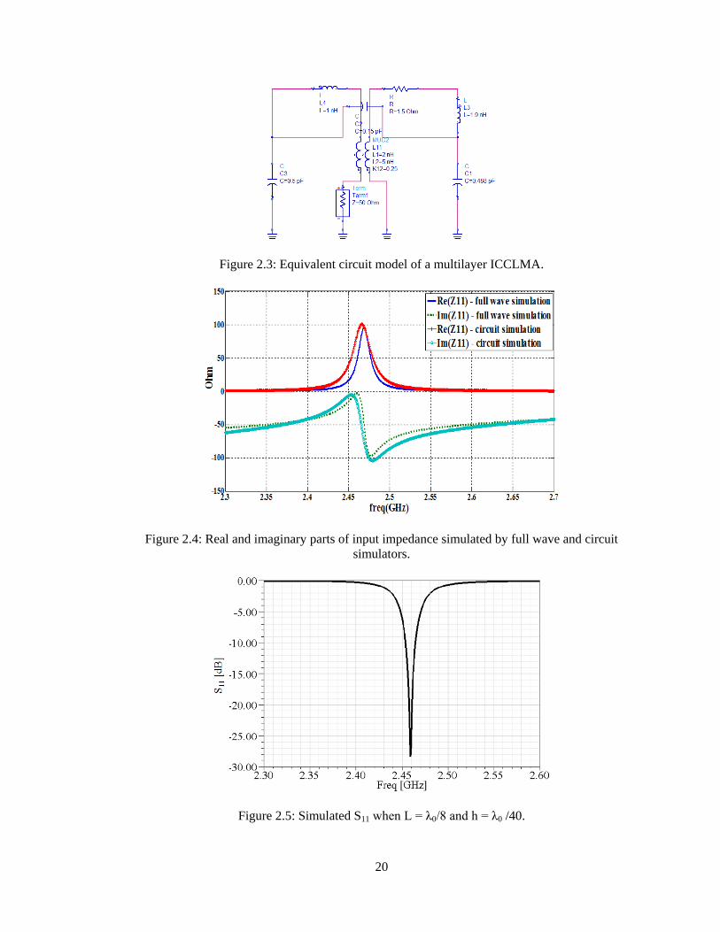
full wave simulation results. Fig. 2.4 shows the real and imaginary parts of input
impedance which are derived from a circuit (Advanced Design System 2009) and full
wave (Ansoft HFSS 12) simulator. It is shown that the two results are in very good
agreement, meaning that the equivalent circuit model can predict the performance
perfectly. Simulated S11 in Fig. 2.5 indicates good impedance matching and fractional 10-
dB return loss bandwidth of 0.45% due to high quality factor.
The vertically (co-) and horizontally (cross-) polarized radiation pattern in the E-
plane and H-plane are presented in Fig. 2.6(a) and (b). The co-polarized radiation pattern
is omnidirectional pattern with the direction of maximum gain occurring at θ = 90°.
While the gain of co-polarized radiation at θ = 90° near ground observation is 0.46 dBi,
the gain of cross-polarized radiation at θ = 90° is less than dBi. As expected, the proposed
antenna provides excellent suppression of horizontally polarized radiation.
Page 41
20
Figure 2.3: Equivalent circuit model of a multilayer ICCLMA.
Figure 2.4: Real and imaginary parts of input impedance simulated by full wave and circuit
simulators.
Figure 2.5: Simulated S11 when L = λ0/8 and h = λ0 /40.
Page 42
21
(a) (b)
Figure 2.6: Simulated (a) E-Plane and (b) H-Plane radiation patterns when L = λ0/8 and h = λ0/40
2.1.2.3 Bench Marking
In this section, the performance of the proposed antenna is compared with those
of other low-profile antennas reported in the literature. This comparison includes the size,
gain, and polarization purity of the proposed antenna against a conventional inverted F
antenna and the multi-element monopole antenna (MMA) introduced in [37]. Two
antennas with the same height (= 3.14 mm = λ0/40) as that of the proposed antenna, are
designed as shown in Fig. 2.7. To address a general drawback of low profile antennas
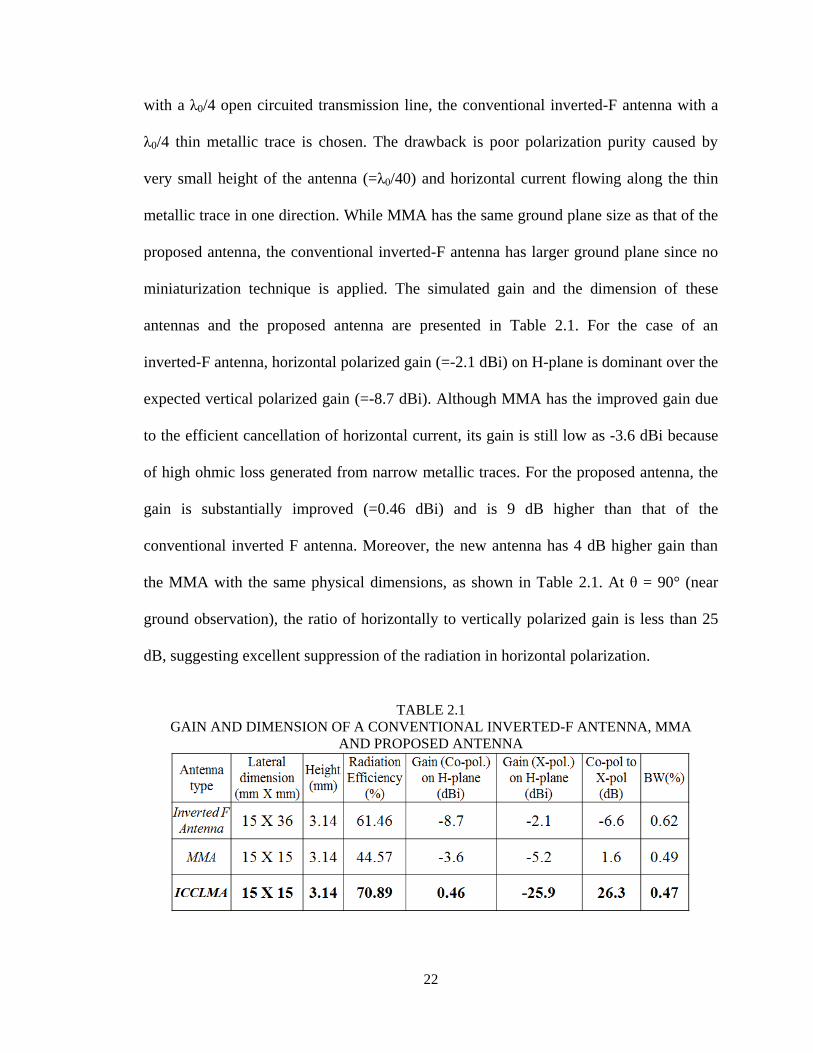
designed using a λ0/4 open circuited transmission line, the conventional inverted-F
antenna with a λ0/4 open circuited transmission line, the conventional inverted-F antenna
Page 43
22
with a λ0/4 open circuited transmission line, the conventional inverted-F antenna with a
λ0/4 thin metallic trace is chosen. The drawback is poor polarization purity caused by
very small height of the antenna (=λ0/40) and horizontal current flowing along the thin
metallic trace in one direction. While MMA has the same ground plane size as that of the
proposed antenna, the conventional inverted-F antenna has larger ground plane since no
miniaturization technique is applied. The simulated gain and the dimension of these
antennas and the proposed antenna are presented in Table 2.1. For the case of an
inverted-F antenna, horizontal polarized gain (=-2.1 dBi) on H-plane is dominant over the
expected vertical polarized gain (=-8.7 dBi). Although MMA has the improved gain due
to the efficient cancellation of horizontal current, its gain is still low as -3.6 dBi because
of high ohmic loss generated from narrow metallic traces. For the proposed antenna, the
gain is substantially improved (=0.46 dBi) and is 9 dB higher than that of the
conventional inverted F antenna. Moreover, the new antenna has 4 dB higher gain than
the MMA with the same physical dimensions, as shown in Table 2.1. At θ = 90° (near
ground observation), the ratio of horizontally to vertically polarized gain is less than 25
dB, suggesting excellent suppression of the radiation in horizontal polarization.
TABLE 2.1
GAIN AND DIMENSION OF A CONVENTIONAL INVERTED-F ANTENNA, MMA
AND PROPOSED ANTENNA
Page 44
23
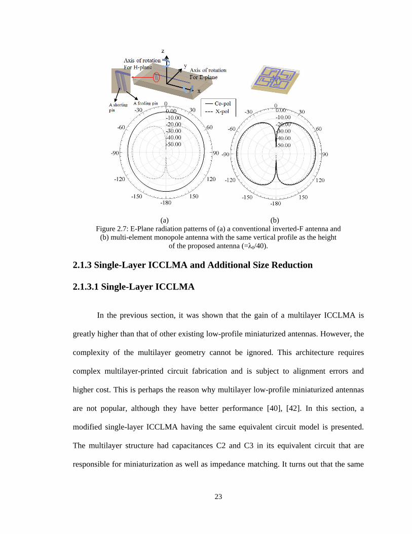
(a) (b)
Figure 2.7: E-Plane radiation patterns of (a) a conventional inverted-F antenna and
(b) multi-element monopole antenna with the same vertical profile as the height
of the proposed antenna (=λ0/40).
2.1.3 Single-Layer ICCLMA and Additional Size Reduction
2.1.3.1 Single-Layer ICCLMA
In the previous section, it was shown that the gain of a multilayer ICCLMA is
greatly higher than that of other existing low-profile miniaturized antennas. However, the
complexity of the multilayer geometry cannot be ignored. This architecture requires
complex multilayer-printed circuit fabrication and is subject to alignment errors and
higher cost. This is perhaps the reason why multilayer low-profile miniaturized antennas
are not popular, although they have better performance [40], [42]. In this section, a
modified single-layer ICCLMA having the same equivalent circuit model is presented.
The multilayer structure had capacitances C2 and C3 in its equivalent circuit that are
responsible for miniaturization as well as impedance matching. It turns out that the same
Page 45
24
capacitances can be realized in single-layer ICCLMA architecture as shown in Fig. 2.8.
The series capacitor C2 between the primary circuit and the secondary circuit is created
by an in-plane interdigital capacitance, and C3 is the shunt capacitance between the strip
attached to the primary circuit (left side of the interdigital capacitor) and the ground plane.
Fig. 2.9 shows the simulated radiation pattern of single-layer ICCLMA having the same
dimension as a multilayer ICCLMA. This antenna has a slightly lower gain of 0 dBi at
the same resonant frequency.
Figure 2.8: Topology of single-layer ICCLMA.
(a) (b)
Figure 2.9: Simulated (a) E-Plane and (b) H-Plane radiation patterns of a single layer ICCLMA
when L = λ0/8 and h = λ0/40.
Figure 2.10: Equivalent circuit model of single-layer ICCLMA.
Page 46
25
Figure 2.11: Design procedure for additional size reduction of single-layer ICCLMA.
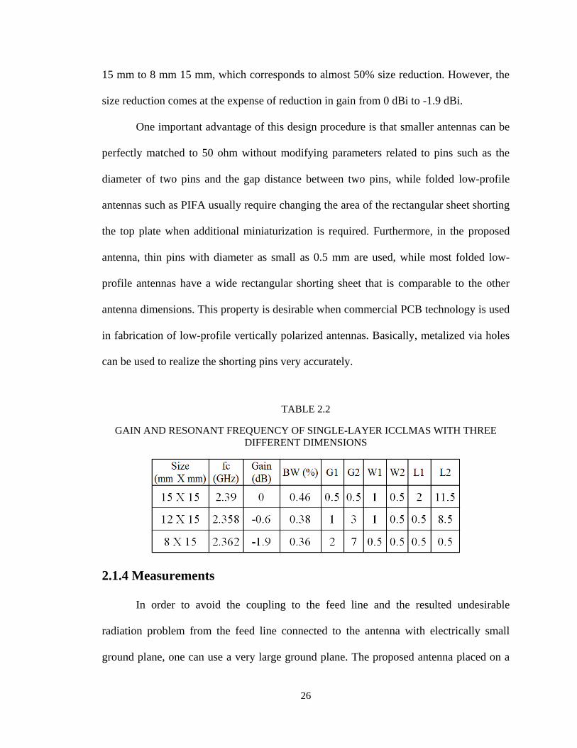
2.1.3.2 Additional Size Reduction of Single-Layer ICCLMA
As discussed in Section 2.1.3.1, the introduction of the series capacitance C2 in
the proposed ICCLMA antenna allows for the ease of impedance matching at lower
frequency. This property also allows for obtaining additional size reduction of single-
layer ICCLMA. Fig. 2.10 shows equivalent circuit model of single-layer ICCLMA.
When C2 is changed by modifying the interdigital structure as shown in Fig. 2.11, C1 and
C3 are also changed at the same time because they are proportional to the area of metal
sheet on the top layer.
It is interesting to note that the proper combination of C1, C2 and C3 values can
achieve excellent impedance matching of smaller antennas. Fig. 2.11 describes how this
principle is applied for additional size reduction. The suitable combination of C1, C2 and
C3 values can be found by changing the gap distance between two metallic sheets on the
top layer (G1 and G2), the width of protruding parts of the interdigital shape (W1 and
W2), as well as L1 and L2. For example, the center prong in Fig. 2.11 determines the
series capacitance C2 and other prongs are modified to get the required capacitance C1.
The impedance matching for three different dimensions is well achieved at the same
resonant frequency as shown in Table 2.2. Finally, the size can be reduced from 15 mm
Page 47
26
15 mm to 8 mm 15 mm, which corresponds to almost 50% size reduction. However, the
size reduction comes at the expense of reduction in gain from 0 dBi to -1.9 dBi.
One important advantage of this design procedure is that smaller antennas can be
perfectly matched to 50 ohm without modifying parameters related to pins such as the
diameter of two pins and the gap distance between two pins, while folded low-profile
antennas such as PIFA usually require changing the area of the rectangular sheet shorting
the top plate when additional miniaturization is required. Furthermore, in the proposed
antenna, thin pins with diameter as small as 0.5 mm are used, while most folded low-
profile antennas have a wide rectangular shorting sheet that is comparable to the other
antenna dimensions. This property is desirable when commercial PCB technology is used
in fabrication of low-profile vertically polarized antennas. Basically, metalized via holes
can be used to realize the shorting pins very accurately.
TABLE 2.2
GAIN AND RESONANT FREQUENCY OF SINGLE-LAYER ICCLMAS WITH THREE
DIFFERENT DIMENSIONS
2.1.4 Measurements
In order to avoid the coupling to the feed line and the resulted undesirable
radiation problem from the feed line connected to the antenna with electrically small
ground plane, one can use a very large ground plane. The proposed antenna placed on a
Page 48
27
large ground plane is measured by a vector network analyzer. It should be pointed out
that the design parameters of the antenna on a large ground plane are slightly different
from those of the same antenna on a small ground plane. A miniaturized single-layer
ICCLMA on 3λ0 X 3λ0 ground plane is designed, fabricated and measured as shown in
the measurement setup of Fig. 2.12. Fig. 2.13 shows the measured reflection coefficient,
compared with the simulation result. A good agreement is observed. Measured radiation
pattern of this antenna is compared to that of a λ0/4 monopole antenna on the same
ground plane. Fig. 2.14 shows the overall gain of the proposed antenna operating at the
resonant frequency is comparable to that of a monopole λ0/4 antenna.
(a) (b)
Figure 2.12: (a) Miniaturized single-layer ICCLMA and (b) measurement set up using a large
ground plane (3λ0 X 3λ0).
Figure 2.13: Measured and simulated S11 of a miniaturized single-layer ICCLMA on a large
ground plane.
Page 49
28
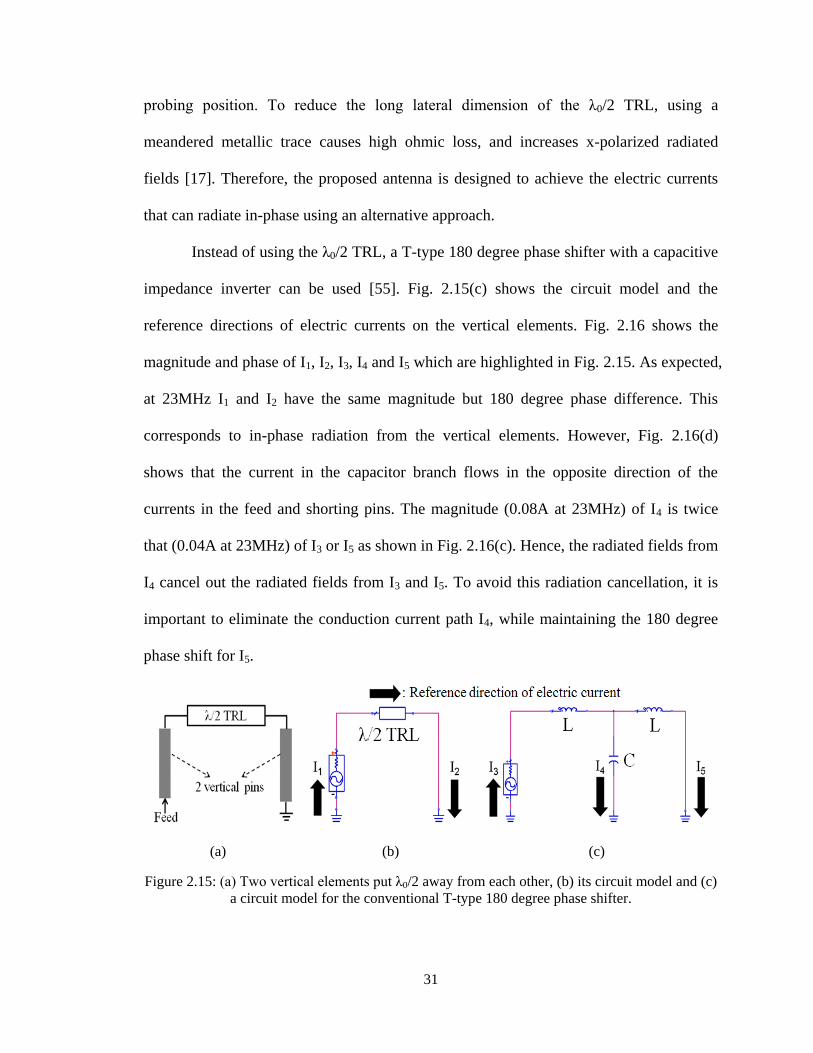
Figure 2.14: Measured E-Plane radiation patterns of a ICCLMA and λ0/4 monopole antenna.
2.2 Extremely Small Two-Element Monopole Antenna
2.2.1 Introduction
Emerging wireless technologies increase the needs for small-size, light-weight
and easily fabricated antennas. A quarter-wave monopole antenna is the most ubiquitous
antenna used for many applications such as unattended ground sensors and ground-based
communication systems at various frequency bands [48], [9]. However, the size of such
antenna is prohibitively large for portable devices operating at low frequencies. This is
particularly a major limiting factor at HF band whose applications for mobile wireless
devices have been limited by the antenna size [49]-[51]. As a type of miniaturized
monopole antenna, low-profile inverted-F antennas (IFA) are most commonly used. One
drawback of these antennas is that as their height decreases, the gain corresponding to
vertically (co-) polarized radiation drops rapidly. This performance degradation is due to
the increased power loss and the increase in radiated power from cross (x-) polarized
Page 50
29
electric currents flowing on metallic traces highly concentrated and meandered in a small
area [40], [17]. However, the horizontal currents are essential in establishing the required
high current level on the short vertical pin which is the main radiating component of the
antennas [17]. In addition, many other types of low-profile electromagnetically coupled
monopole antennas have been reported in the literature. In [18]–[23], capacitively loaded
monopole antennas with different special disk geometries are presented for reducing the
antenna height and improving the bandwidth. The height of these antennas is typically in
the range of λ0/10 with excellent operational bandwidth. However, their lateral
dimensions are comparable to the wavelength. In [17], a new type of low-profile
miniaturized monopole antenna utilizing inductive coupling and capacitive loading was
reported. In this approach, significant size reduction (λ0/45 X λ0/16 X λ0/8) is reported
while polarization purity and high gain are maintained.
Recently, an antenna miniaturization technique using chip inductors has been
investigated [23], [52]-[54]. In [53] and [54], the chip inductors are embedded into the
printed monopole antennas to decrease the size of the antennas at the expense of gain and
bandwidth. To make the size of the antennas small enough for portable wireless devices,
extreme miniaturization must be attempted when the typical size of the antennas is
comparable to or smaller than λ0/100. At these small dimensions, all antenna components
act as lumped elements. Utilization of chip inductors and capacitors with poor quality
factor for the antenna structure lowers radiation efficiency.
In this work, a novel design for extremely small HF monopole antennas is
presented. The proposed antenna utilizes two short vertical elements producing in-phase
radiated fields. In this way, the effective height of the short dipole is increased without
Page 51
30
physically increasing the height. This leads to enhanced gain compared to a short
monopole with the same height [55]. In order to achieve the in-phase radiated fields from
electric currents flowing on the two vertical elements, a novel antenna topology using a
modified T-type 180 degree phase shifter is introduced. It is shown that increasing the
quality factor (Q) of the inductors used in the phase shifter can lead to significant gain
enhancement. For example, it is shown that optimized air-core inductors can improve the
gain by a factor of 14 (=11.3dB) compared to a commercial chip inductor. The basic idea
is presented in Section 2.2.2. Design, implementation and performance assessment of the
proposed HF antenna using chip inductors are presented in Section 2.2.3. In Section 2.2.4,
we discuss gain enhancement using optimized air-core inductors and the approach for
incorporating such inductors within the antenna volume. In Section 2.2.5, the proximity
effect of objects on the resonant frequency of the proposed antenna with narrow
bandwidth is investigated.
2.2.2 Realization of Two In-Phase Radiating Vertical Elements Using a
Modified T-Type 180 Degree Phase Shifter
Let us imagine a short-circuited λ0/2 transmission line (TRL) resonator connected
to two shorting pins at both ends. Large electric currents on the two shorting pins can
radiate vertically polarized fields that are in phase. Fig. 2.15(a) shows two vertical
elements (pins) connected by a λ0/2 TRL. Radiated fields from the electric currents
flowing on the two vertical pins are in phase because of the 180 degree phase shift from
the λ0/2 TRL. The corresponding circuit model is shown in Fig. 2.15 (b), assuming that
small inductances from the two vertical pins with very low profile (<<λ0/100) can be
ignored. The black arrow depicts the reference direction of the electric current at each
Page 52
31
probing position. To reduce the long lateral dimension of the λ0/2 TRL, using a
meandered metallic trace causes high ohmic loss, and increases x-polarized radiated
fields [17]. Therefore, the proposed antenna is designed to achieve the electric currents
that can radiate in-phase using an alternative approach.
Instead of using the λ0/2 TRL, a T-type 180 degree phase shifter with a capacitive
impedance inverter can be used [55]. Fig. 2.15(c) shows the circuit model and the
reference directions of electric currents on the vertical elements. Fig. 2.16 shows the
magnitude and phase of I1, I2, I3, I4 and I5 which are highlighted in Fig. 2.15. As expected,
at 23MHz I1 and I2 have the same magnitude but 180 degree phase difference. This
corresponds to in-phase radiation from the vertical elements. However, Fig. 2.16(d)
shows that the current in the capacitor branch flows in the opposite direction of the
currents in the feed and shorting pins. The magnitude (0.08A at 23MHz) of I4 is twice
that (0.04A at 23MHz) of I3 or I5 as shown in Fig. 2.16(c). Hence, the radiated fields from
I4 cancel out the radiated fields from I3 and I5. To avoid this radiation cancellation, it is
important to eliminate the conduction current path I4, while maintaining the 180 degree
phase shift for I5.
(a) (b) (c)
Figure 2.15: (a) Two vertical elements put λ0/2 away from each other, (b) its circuit model and (c)
a circuit model for the conventional T-type 180 degree phase shifter.
Page 53
32
(a) (b) (c) (d)
Figure 2.16: (a) Magnitudes and (b) phases of I1 and I2, and (c) magnitudes and (d) phases of I3, I4
and I5 shown in Fig. 2.15.
(a) (b)
Figure 2.17: (a) Circuit model for a T-type 180 degree phase shifter and (b) circuit model
employing an open stub instead of a grounded capacitor in (a).
(a) (b)
Figure 2.18: (a) Magnitudes and (b) phases of I6 and I7 shown in Fig. 2.17.
Page 54
33
The conduction current I4 can be eliminated altogether by replacing the lumped
capacitor with an open-stub as shown in Fig. 2.17(b). Characteristic impedance and
length of the open stub in the circuit schematic are appropriately chosen to achieve the
required 180 degree phase shift at 23MHz. Fig. 2.18 shows the magnitudes and phases of
I6 and I7, indicating the same magnitude and 180 degree phase difference for achieving
efficient vertically polarized radiation.
2.2.3 Extremely Small Two-Element Monopole Antenna Configuration
2.2.3.1 Antenna Design
Based on the equivalent circuit model shown in Fig. 2.17(b), an extremely low-
profile miniaturized HF antenna with two in-phase radiating vertical elements is designed.
Fig. 2.19 shows the side view and the top view of the proposed antenna. The lateral
dimension and height of the proposed antenna including the ground plane are 150mm
(0.0115λ0) and 50mm (0.0038λ0), respectively. The top metallic plate acts as the open
stub (capacitor of the phase shifter) connected between the two chip inductors (8µH)
which are connected to the vertical pins. The substrate used in this design is air, allowing
elimination of dielectric loss from the antenna structure. In order to include ohmic loss in
the simulation, the finite conductivity of copper is used in all metallic traces and the two
vertical pins. In order to consider actual characteristics of the chip inductors, equivalent
series resistance (ESR) of 28ohm is extracted at 23MHz from the datasheet provided by
the manufacturer [56]. The ESR is included in the simulation for calculation of antenna
input impedance and radiation efficiency. By optimizing the distance between the
shorting pin and the feeding pin appropriately, impedance matching to a 50ohm feed is
Page 55
34
obtained. The geometry of the open stub on the top plate is chosen to be symmetric in
terms of xz and yz planes and the positions of the two pins are chosen near the center of
antenna structure to obtain omnidirectional radiation pattern.
Fig. 2.20(a) shows the simulated S11 of the proposed antenna with the center
frequency of 23.2MHz. It should be noted that using a coaxial feed cable to measure S11
of the monopole antennas having a very small ground plane (0.0115λ0 X 0.0115λ0)
produces incorrect results. This is due to the strong near-field coupling between the
antenna and outer conductor of the coaxial cable. The excited induced currents over the
cable produce changes in radiation pattern and S11 [17]. To avoid this measurement
problem, a small source module can be connected to the antenna feed. Fig. 2.21 shows
the fabricated antenna integrated with the small source module consisting of a Voltage
Controlled Oscillator (VCO), potentiometer and a 12V battery. By controlling the
potentiometer, the bias voltage of the VCO can be changed, enabling frequency tuning.
By observing the variation of received power versus frequency, the operating (resonant)
frequency of the antenna is found. This is done using the proposed antenna with chip
inductors as a transmitting antenna and using a λ0/10 dipole antenna with a wider
bandwidth as a receiving antenna. Fig. 2.20(b) shows the setup used to measure the
received power and the radiation patterns of the proposed antenna. The transmitting
antenna (the proposed antenna) is mounted on a positioner, and the receiving antenna
(λ0/10 dipole antenna) is mounted in an elevated position. By using this elevated range,
the measurement error caused by the reflected waves from the ground can be decreased
substantially. In order to calculate the measured gain of the proposed antenna, λ0/10
dipole antennas are used, as reference antennas.
Page 56
35
As mentioned earlier, S11 of the proposed antenna cannot be measured directly by
a network analyzer due to the near-field coupling. However, it can be indirectly evaluated
by comparing the slope and the center frequency of the measured received power versus
frequency to those of the simulated response. Fig. 2.22 shows measured and simulated
power received by the λ0/10 dipole antenna in an elevated range versus frequency. The
power is normalized by the peak value of each plot for a better slope comparison between
the measured and simulated plots. It is shown that the slope of the measured plot is
similar to that of the simulated plot, indicating that S11 of the fabricated antenna is well
matched to the simulated S11. Measured resonant frequency is 22.9MHz which is slightly
shifted from the simulated resonant frequency of 23.2MHz due to the 5% tolerance range
of the commercial chip inductors. Based on simulated S11, 10-dB return loss bandwidth
of 0.86% is derived at 23.2MHz. Fig. 2.23 shows measured and simulated radiation
patterns in the E (yz) plane and H (xy) plane. Omnidirectional radiation patterns are
observed. The measured antenna gain is -29.2dBi, which is similar to the simulated gain
of -28.1dBi.
(a) (b)
Figure 2.19: (a) Side view and (b) top view of the proposed antenna with chip inductors.
Page 57
36
(a) (b)
Figure 2.20: (a) Simulated S11 of the proposed antenna with chip inductors and (b) measurement
setup in an elevated antenna range.
Figure 2.21: Fabricated antenna with chip inductors, integrated with the source module.
Figure 2.22: Measured and simulated power received at the reference λ0/10 dipole antenna and
normalized by the peak value of each response versus frequency when the proposed antenna with
chip inductors is used as a transmitting antenna.
Page 58
37
(a) (b)
Figure 2.23: Measured and simulated radiation patterns of the proposed antenna with chip
inductors in the (a) E (=yz) plane and (b) H (=xy) plane.
2.2.3.2 Gain and Mass Comparison
To examine a figure of merit of the proposed antenna, its gain and mass are
compared with those of a conventional inverted-F antenna having the same dimensions
and volume. A small inverted-F antenna can be fabricated using a λ0/4 open-ended
transmission line on a high index substrate material. The free space wavelength (λ0) at
22.9MHz is 13.1m and thus λ0/4 is 3.275m. Fitting a λ0/4 inverted-F antenna on very
small area of 150mm X 150mm (0.0115λ0 X 0.0115λ0) is not practical. Thus, the use of a
substrate with high dielectric constant (εr=10.2 and tan δ=0.002) is necessary. A spiral
geometry is used to accommodate the quarter-wave transmission line as shown in Fig.
2.24. Fig. 2.25 shows the simulated S11 of the spiral-shaped inverted-F antenna,
compared to that of the proposed two-element short monopole antenna. It is found that
10-dB return loss bandwidth of the spiral-shaped IFA is much narrower than that of the
Page 59
38
proposed antenna due to the highly stored electric energy in the high dielectric substrate.
Fig. 2.26 shows the simulated radiation patterns in the E-plane and H-plane of the spiral-
shaped IFA. The gain of the spiral-shaped IFA is calculated as -34.4dBi which is 5.2dB
lower than the measured gain of the proposed antenna. This is due to the ohmic loss in
the spiral trace and dielectric losses, despite a very good dielectric loss tangent (tan
δ=0.002). This result suggests that the parasitic losses from the two chip inductors in the
proposed antenna are much lower than the ohmic and dielectric losses in the spiral-
shaped IFA. It is also found that the proposed two-element short monopole antenna
provides wider bandwidth than the spiral-shaped IFA.
Another advantage of the proposed two-element short monopole antenna over the
IFA is its much lower mass. The substrate materials with high dielectric-constant usually
have high mass density which makes the antenna that uses such substrates heavy. The
proposed antenna provides miniaturization without the need for high index materials and
thus it can be made very light. Table 2.3 shows the masses of all the materials used to
fabricate the spiral-shaped IFA with a substrate having εr=10.2 and the proposed antenna
with air substrate. The total mass of the conventional inverted-F antenna (3502g) is about
220 times heavier than that of the proposed antenna (15.8g). Fig. 2.27 shows the
proposed antenna fabricated using flexible thin substrates.
Figure 2.24: Spiral-shaped inverted-F antenna on the substrate with εr =10.2.
Page 60
39
Figure 2.25: Simulated S11 of spiral-shaped inverted-F antenna on the substrate with εr =10.2,
compared to that of the proposed antenna with chip inductors.
(a) (b)
Figure 2.26: Simulated radiation patterns of spiral-shaped inverted-F antenna on the substrate
with εr =10.2 in the (a) E (=yz) plane and (b) H (=xy) plane.
Figure 2.27: Proposed antenna fabricated using flexible thin substrates.
Page 61
40
TABLE 2.3
MASS OF EACH PART OF THE PROPOSED ANTENNA WITH AIR SUBSTRATE AND
THE SPIRAL-SHAPED INVERTED-F ANTENNA ON THE SUBSTRATE WITH εr=10.2
2.2.4 Gain Enhancement Using Optimized Air-Core Inductors
As discussed in Section 2.2.3.2, the proposed two-element antenna provides
higher gain than the conventional spiral-shaped IFA. This section shows that further gain
enhancement can be achieved by increasing the Q of the inductors used in the phase
shifter. This is possible because Q of the commercial chip inductor is rather low (Q=45).
Fig. 2.28 shows simulated gain of the proposed antenna versus Q of the inductors. It
indicates that increasing Q of the chip inductors from 45 to 450 can lead to gain
enhancement of about 10dB. The relationship between the gain and Q of the inductors is
almost linear up to about Q 104. Beyond the value, radiation resistance in the proposed
antenna dominates over losses on the metallic surfaces. The gain will saturate to the gain
of the ideal short dipole (1.76dBi) if one were to ignore metallic losses.
It is reported that Q of air-core inductors can be as high as several hundred at HF
band due to the absence of the ferrite core loss [57]-[61]. In this section, design and
performance of an extremely small two-element monopole antenna using air-core
inductors are discussed. Since air-core coils have lower inductance values than the
Page 62
41
ferromagnetic core coils, the size of the inductors must be increased. Therefore, the most
important design issue determining antenna gain is to optimize Q of air-core inductors
restricted by the size of the antenna.
Figure 2.28: Simulated gains of the proposed antennas with chip inductors versus Q of the chip
inductors.
2.2.4.1 Optimization of Quality Factor of Air-Core Inductors
The Q of an air-core inductor is determined by two loss mechanisms related to
proximity effect and skin effect. The proximity effect refers to the concentration of electric
currents on a small portion of wires due to the proximity of the adjacent wires in the
inductor coil. This proximity effect can significantly increase AC resistance of adjacent
conductors when compared to its DC resistance. The adverse proximity effect on the AC
resistance increases with frequency. At higher frequencies, the AC resistance of a
conductor can easily exceed ten times its DC resistance [62]. Recently, methods for
accurate prediction of inductance and AC resistance of coils at high frequencies have been
reported [63]-[64]. In [63], the coil is analytically modeled as a slow-wave anisotropic
Page 63
42
waveguide and analytic formulas to determine the inductance and AC resistance are
presented. The formulas are corrected based on experimental data as presented in [64]-
[65]. Fig. 2.29 shows design parameters of the coil, and (2.1) and (2.2) are the analytic
formulas including the correction factor derived from experimental data to calculate the
inductance and AC resistance.
Figure 2.29: Design parameters of the air-core coil.
Based on the literatures, the inductance is given by
L=(µ0πD2 N
2kL/4l)-[µ0DN(ks(e)+km)/2]+Li (2.1)
where D is the effective current-sheet diameter, N is the number of turns, l is the coil
length, Li is the internal inductance, kL is Nagaoka's coefficient, km is Rosa's mutual-
inductance correction term presented in [64], and ks(e) = (3/2)-ln(2p/d) where d is the
diameter of the wire and p is the winding pitch-distance
The AC resistance is given by
RAC=RDC[1+ (Ω-1) ψ(N-1+1/ ψ)/N] (2.2)
Page 64
43
where RDC is DC resistance, ψ is proximity factor (derived by the interpolation of
Medhurst’s table of experimental data [65]) and Ω=d2/[4(dδi-δi
2)] where δi=skin depth.
Based on (2.1) and (2.2), dimension parameters of an air-core solenoid with
inductance of 8µH are optimized considering the constrained antenna volume of 150mm
X 150mm X 50mm. In order not to increase vertical profile of the antenna, the coil is
placed between the ground plane and the top plate, which limits the diameter of the coil to
be strictly smaller than 50mm. In the proposed antenna, 25mm is chosen for the coil
diameter in order not to drastically increase the top plate capacitance. With the fixed coil
diameter (D), the effects of coil length (l) and wire diameter (d) on Q are investigated.
Once the values of D and l (or d) are chosen and fixed, the values of other parameters such
as the number of turns (N) and the winding pitch-distance (p) are accordingly determined
to achieve the required inductance of 8µH. Fig. 2.30(a) shows the calculated Q versus l
where d is 1mm. This figure suggests that increasing l after about l=60mm doesn’t affect
Q of the inductor. This is due to the fact that the proximity effect vanishes once wires are
far from each other (large p). 70mm is chosen as the optimum value of l. With the chosen
l=70mm, the effect of d is iteratively examined. Fig. 2.30(b) shows Q versus d where l is
70mm. The figure suggests that increasing d beyond d=1mm, the Q of the inductors
decreases because p decreases with fixed l, leading to the increase in the proximity effect.
Finally, the values of D, N, l, d and p are chosen as 25mm, 32, 70mm, 1mm and 2.3mm,
respectively, resulting in a quality factor of about 730.
Page 65
44
(a) (b)
Figure 2.30: Calculated Q versus (a) l (=coil length) where d = 1 mm, and (b) d (=wire diameter)
where l = 70mm.
2.2.4.2 Antenna Design
The air-core solenoids designed in the previous section are used to design an
extremely small two-element monopole antenna. Fig. 2.31 shows the geometry of the
proposed antenna with the same dimensions as the previous antenna where chip inductors
were used. As mentioned earlier, the solenoids are integrated underneath the capacitive
loading plate not to increase the overall vertical profile of the antenna. The copper layer
over the area where the solenoids are positioned is removed to reduce the effect of the top
metallic plate on the inductance and the effect of the solenoids on the top plate capacitance.
An additional shorting pin with a chip inductor of 40nH is used to get impedance
matching to a 50Ohm feed. Fig. 2.32 shows the side and bottom view of the fabricated
antenna integrated with the source module.
Fig. 2.33 shows the simulated S11 of the antenna with air-core inductors,
compared to that of the antenna with chip inductors. As expected, the bandwidth of the
antenna with air-core inductors (10-dB return loss bandwidth of 0.13% at 22.1MHz.) is
narrower than that of the antenna with chip inductors due to very high Q (≈730) of the
air-core inductors. As discussed in Section 2.2.3.1, S11 of the proposed antenna cannot be
Page 66
45
measured directly by a network analyzer due to the aforementioned near-field coupling.
As before, the center frequency and the bandwidth are characterized through transmission
measurement. Fig. 2.34 shows the measured and simulated power received at the
reference λ0/10 antenna as a function of frequency. The power is normalized by the peak
value of each response to compare the different plots. It is shown that the slope of the
measured response of the antenna with air-core inductors is much steeper than that of the
antenna with chip inductors, showing good agreement with the simulated plot. Measured
resonant frequency is 22.9MHz which is slightly different from the simulated resonant
frequency of 22.1MHz due to the interaction between the solenoids and other metallic
parts. Fig. 2.35 shows the measured and simulated radiation patterns in the E (=yz) plane
and H (=xy) plane. Omnidirectional radiation patterns are observed and measured
antenna gain is found to be -17.9dBi. This is 11.3dB and 16.5dB higher than that of the
antenna with chip inductors and the spiral-shaped IFA, respectively. The total mass of the
antenna with two air-core solenoids made of copper is 51.95g.
Figure 2.31: Geometry of the proposed antenna with air-core inductors having the dimensions of
150mm X 150mm X 50mm.
Page 67
46
(a) (b)
Figure 2.32: (a) Side view and (b) bottom view of the fabricated antenna incorporating air-core
inductors, integrated with the source module.
Figure 2.33: Simulated S11 of the proposed antenna with air-core inductors, compared to that of
the antenna with chip inductors. Narrower bandwidth indicates higher radiation efficiency
because the antenna volume is fixed.
Figure 2.34: Measured and simulated power received at the reference λ0/10 antenna and
normalized by the peak value of each response versus frequency when the proposed antenna with
air-core inductors is used as a transmitting antenna, compared to those of the antenna with chip
inductors.
Page 68
47
(a) (b)
Figure 2.35: Measured and simulated radiation patterns of the proposed antenna with air-core
inductors in the (a) E (=yz) plane and (b) H (=xy) plane.
Since the sizes of the antennas under discussion are electrically very small, it is
interesting to compare the performance of the antennas to the fundamental limit derived
by [66]. To do that, a figure of merit is used, defined as the product of the 3-dB return
loss bandwidth (BW) and radiation efficiency (η). Fig. 2.36 shows the figures of merit
corresponding to the antennas, electrical small antennas in literature and the fundamental
limit. The 3-dB return loss bandwidth (BW) of the fundamental limit is calculated using
BW=1/Q where Q≈1/(kr)3 where k is the wave number and r is the radius of the smallest
sphere that can enclose the antenna. The results suggest that although the bandwidth of
the antenna with air-core inductors is narrower than those of the antenna with chip
inductors and the spiral-shaped IFA, because the radiation efficiency of the antenna with
air-core inductors is tens of times higher than those of others, the figure of merit of the
antenna with air-core inductors gets much closer to the fundamental limit than the other
Page 69
48
antennas. With this analysis, it is successfully validated that the proposed electrically
small antenna provides significantly enhanced performance, compared to the
conventional IFA.
Figure 2.36: Performance comparison among the electrically small antennas shown in this work.
2.2.5 Proximity Effect of Nearby Objects
For very small antennas with narrow bandwidth, there is always a concern about
the proximity effect of nearby objects as regards the possible shift in resonant frequency.
At HF band where the wavelength is large, typical distances between the small antennas
and nearby objects in an indoor environment are very small compared to the wave length.
In order to examine the feasibility of using the proposed antennas for such environments,
the change in the operating frequency caused by nearby objects is investigated. This is
done experimentally by changing the distance between the antenna and a concrete wall,
and the ground in an indoor environment. Fig. 2.37 shows the measurement set up. At
wall separation distance (s) = 0.5, 1, 1.5 and 2m, and ground height (h) = 0.2m and 1.4m,
the power received at the λ0/10 dipole antenna is measured and normalized by the peak
value of each plot when the proposed antenna with air-core inductors is used as a
Page 70
49
transmitting antenna. Fig. 2.38 shows the measurement results, indicating a stable
operating frequency of the proposed antenna. The small variation observed is due to
frequency jitter of the VCO itself. Also the frequency response of a λ0/10 dipole antenna
as the transmitting antenna when the same λ0/10 dipole antenna is used as the receiving
antenna, is shown to indicate that the observed steep frequency response is due to the
frequency response of the proposed two-element monopole antenna.
Figure 2.37: Measurement set up for examining the proximity effect of nearby objects on the
resonant frequency of the proposed narrow band antenna.
Figure 2.38: Measured received normalized power corresponding to various positions of the
transmitting (=proposed) antenna shown in Fig. 2.37.
Page 71
50
Chapter 3
Realization of Omnidirectional Radiation Pattern/Broad
Bandwidth for Low Profile Antennas on a Small Ground Plane
In this chapter, techniques are presented to realize omnidirectional radiation
pattern for low profile antenna on a small ground plane (<<λ). Based on these techniques,
an antenna embedded into small robotic platforms is designed and its performance is
discussed. In addition, a broadbanding technique compatible with the miniaturization
techniques for realizing omnidirectional radiation pattern is presented.
3.1 Low Profile Balanced-Type Omnidirectional Antennas
3.1.1 Introduction
Recent development in wireless device technologies urges antennas to be
integrated with very small ground plane. However, such antennas on the small ground
plane (<< λ0) suffer from serious distortion in radiation pattern. In this section, we try to
propose a design approach for low profile omnidirectional antennas by addressing a
problem in characterizing the input impedance and radiation pattern of such antennas
with unbalanced feed. For measuring the input impedance using a network analyzer or
Page 72
51
the radiation pattern using a spectrum analyzer, a coaxial cable must be connected to the
antenna. The problem is that the antenna with the small ground plane is coupled to the
coaxial cable over which an electric current can get excited. As a result, both the input
impedance and the radiation pattern of the antenna are changed. Fig. 3.1 depicts the
electric field distribution around the proposed antenna fed by a coaxial cable. Significant
electric current exists on the external layer of the coaxial cable that unexpectedly
contributes to radiation. This causes a shift in the resonant frequency, poor impedance
matching and radiation pattern. Although omni-directional radiation pattern is expected
(see Fig. 3.2(a)), deformed radiation pattern is measured as shown in Fig. 3.2(b). At
θ=90°, which is in the azimuthal plane of ICCLMA, the gain drops from 0 dBi to -8 dBi.
Figure 3.1: Electric field distribution in the proposed antenna fed by coaxial cable.
(a) (b)
Figure 3.2: Simulated E-Plane radiation pattern of single-layer ICCLMA (a) without and (b) with
a coaxial cable.
Page 73
52
3.1.2 Balanced Type of ICCLMA
Miniaturized monopole antennas are considered for wireless nodes with small
platforms where the back of the antenna ground plane can support the active elements. As
described in the previous section, the characterization of small antennas by connecting a
long coaxial cable leads to uncertainties in the antenna radiation parameters. One
approach is to use large ground planes (>λ0 on each side) as was shown in Section 2.1.4,
but at low frequencies the size of the ground plane may become prohibitively large. To
avoid this problem, an alternative method to measure the input impedance and radiation
pattern of electrically small antennas is presented. This can be done using a balanced
architecture or simply the dipole version of the monopole antenna (see Fig. 3.3). A
balanced architecture produces a null surface in the plane bisecting the dipole structure.
In this plane, any metallic structure like the antenna feed can be inserted without
affecting the antenna characteristics. The only difficulty is that a balun structure must be
used. Although measuring a balanced version of the antenna is not representative of the
performance of the antenna on small ground, by redesigning and testing the antenna on
small ground as a balanced topology it can be examined whether the simulation results of
the antenna previously designed on small ground is trustable or not.
Fig. 3.4 shows a balanced low-profile miniaturized antenna connected to a
microstrip balun in the null plane. The standard microstrip tapered balun is connected to
two back-to-back ICCLMAs. The vertical dimensions of the antenna and balun set up
shown in Fig. 3.4 are given by h1 = 3.175mm and h2 = 0.787mm. Fig. 3.5 shows the
measured and simulated reflection coefficients of a balanced architecture. The simulated
fractional 10-dB return loss bandwidth is 0.78%, while that of 8mm X 15mm single
Page 74
53
ICCLMA with small ground plane is 0.36%. The simulated and measured gains in Fig.
3.6 are 0.66 dBi and 0.36 dBi, which are higher than that of 8mm X 15mm single
ICCLMA with small ground plane. This is not a surprise because the volume of the
dipole ICCLMA is twice that of the monopole version. In Fig. 3.6, measured radiation
pattern shows good agreement with the simulated results. We also tested the antenna with
different length of balun and feed line, and found out that the antenna input impedance
and radiation pattern remain unchanged regardless of the length of the feeding lines.
Therefore, placing active components with differential (=balanced) outputs in the null
plane, this balanced architecture can be used for small RF platforms requiring purely
vertically polarized radiation.
Figure 3.3: Measurement method using a balanced architecture.
Figure 3.4: Side, top and bottom views of measurement set up of a balanced miniaturized antenna
compatible with unbalanced measurement system.
Page 75
54
Figure 3.5: Measured and simulated S11 of the proposed balanced architecture.
(a) (b)
Figure 3.6: Measured and simulated (a) E-Plane (=XZ-Plane) and (b) H-Plane (=XY-Plane)
radiation patterns of the proposed balanced architecture.
3.1.3 Application of Low Profile Balanced-Type Antenna
In this section, a low Profile balanced-type vertically polarized omnidirectional
antenna structurally embedded into a compact crawling spy robot is presented. There are
Page 76
55
mainly three challenging objectives in designing this type of antenna. The first objective
is to get high gain for vertical polarization from a low-profile configuration. Fig. 3.7(a)
depicts the layouts corresponding to top, middle and bottom layers of a crawler. As
shown in Fig. 3.7(b), the space of 19mm X 19mm is considered for a vertically polarized
antenna. Fig. 3.8 shows how embedded antenna is integrated with Bluetooth module. It
says that the available height to be able to contribute to vertically polarized radiation is
just 8mm, which is λ/16. The second objective is to design an antenna structure to be able
to compensate distorted and limited ground plane near the radiator generated by bending
a paper, which result in low gain related to vertically polarized radiation.
(a) (b)
Figure 3.7: (a) Layout of Crawling Robot and (b) location and space for antenna.
Figure 3.8: Integration of an embedded antenna with Bluetooth module.
The third objective is to suppress the radiation from the extended feeding line
connected to Bluetooth module as shown in Fig. 3.8.
Location for Embedded Antenna
Bluetooth module
Antenna pattern
8mm
Page 77
56
One can design ordinary meandered monopole antenna similar to an antenna used
in cell phone, as shown Fig. 3.9(a). However, it turns out that this antenna has very poor
gain of -7.8 dB near ground at θ=90° as shown in Fig. 3.9(b). It explains why antenna
design based on given limitations is challenge.
(a) (b) (c)
Figure 3.9: (a) Meandered monopole antenna, (b) 2D and (c) 3D radiation pattern of v-pol.
The idea to suppress the radiation from horizontal current on the extended feeding
line is to make it ideal transmission line by putting extended ground near feeding line.
As shown in Fig. 3.10, it can be achieved by choosing the gap distance between the
feeding line and extended ground. Moreover, a balanced structure is designed to achieve
omnidirectional radiation pattern related to vertical polarization. It should be noted that
ideal omnidirectional pattern enable to maximize the gain of vertical polarization at
θ=90°.
Figure 3.10: Suppression of radiation from horizontal current using extended ground.
Extended ground Change
Page 78
57
Fig. 3.11 shows the geometry of the proposed antenna and its surface current
distribution. A balanced structure contributes to symmetry radiation pattern of vertical
polarization. Furthermore, Instead of a λ/4 resonator, the design of a λ/2 resonator
generates in-phase two radiating elements for vertical polarization, as shown in Fig.
3.11(b). Fig. 3.12 shows 2D and 3D radiation patterns of the proposed antenna, showing
desirable ideal omnidirectional pattern. The gain of v-pol at θ=90° is improved to 0.12 dB
which is about 8dB higher than the gain of ordinary meandered monopole antenna.
(a) (b)
Figure 3.11: (a) The proposed antenna and (b) its surface current distribution.
Figure 3.12: 2D and 3D radiation patterns of the proposed antenna.
It is required to consider the dielectric constant of paper in which the proposed
antenna is embedded. Since dielectric constant is 1.8, the resonant frequency of antenna
Page 79
58
structure in Fig. 3.11 is changed a little bit, thus the resonant length is reduced in order to
maintain desirable resonant frequency, 2.4GHz. Fig. 3.13 shows simulation model and
results of embedded antenna inside paper.
Figure 3.13: Embedded antenna inside paper and its 2D/3D radiation patterns.
- Fabrication of crawler antennas to be embedded in thin paper
The proposed antenna needs to be fabricated on very thin film in order to provide
flexibility, which enables the bending connection between feeding line and an antenna. It
is difficult to fabricate antennas on films only using general substrate-processing
technology such as milling and chemical etching. Suitability and drawbacks of various
fabrication methods are investigated. Fig. 3.14 shows three popular fabrication methods
(Lift-off, Shadow mask and Etch-back). In the Lift-off method, Photoresist (PR) is first
deposited on a polyester sheet and exposed to light with a proper mask. Depending on the
polarity of PR, PR corresponding to the antenna pattern is removed or remained. This
process is finished by depositing metal on the patterned PR and then dissolving the rest of
PR which is covered with metal. The metal over PR is also removed when PR is
dissolved and only the areas where there was no PR will be covered by metal. The
drawback of this process is the difficulty of dissolving thick PR of 2μm totally at the first
step. Shadow Mask is also a popular process for depositing a thick metal layer. However,
this method is not appropriate for the wing antennas since the isolated thin patterns
between metallic traces in the center of MASK cannot be supported. Therefore, we used
Page 80
59
the Etch-back method to fabricate wing antennas. In this method, the metal is first
deposited and PR deposited next. Similar to Lift-off, the exposed PR forms the desirable
pattern. After etching metal, the covered PR on the metal patterns is removed. Based on
this method, 2µm Gold layers is deposited on 25µm polyimide using sputter and etched
chemically.
(a) (b) (c) Figure 3.14: (a) Lift-off, (b) Shadow mask, and (c) Etch-back.
Fig. 3.15 shows equipment for etch-back process. The function of photoresist
laminator is to put photoresist (PR) on the thin film of up to 12 inch width with high
pressure and temperature (105°C). Exposure machine allows large PR of up to 40cm by
40cm to expose to the light. Magnetron sputtering system is chosen for thin film
deposition since it provides stronger adhesion, compared to evaporator machine.
(a) (b) (c)
Figure 3.15: (a) Photoresist laminator, (b) exposure machine, and (c) sputtering system.
Some problems had to be handled to fabricate antennas on very thin film, as
shown in Fig. 3.16. Firstly, sputtering causes tensile stress problem. It is very serious
problem for the deposition of thick metal (>2μm) on thin film (25μm). In order to reduce
the tensile stress generated during sputtering, the position of the source is properly
Film
Film
Metal
PR Shadow mask
Putting Silver Paste here
Film
Etching uncovered Metal
Page 81
60
controlled. Secondly, long deposition times cause the damage of PET such as melting due
to high temperature. Fabrication conditions such as deposition time and target position
were properly optimized to solve these problems.
(a) (b) (c)
Figure 3.16: (a) Commercial PET (Polyester) film, (b) rolled thin film by tensile stress and (c)
damaged metal surface by high temperature.
- Measurement set up and results for crawler antennas
Fig. 3.17 shows fabricated antennas including alignment keys to be matched
exactly with the layout of a crawler robot. It is embedded in between top and bottom
carbon papers after aligned carefully. Laser cut path of carbon papers for embedded
antenna is shown in Fig. 3.17. Fig. 3.18 shows measurement set up and its simulation
model. Coaxial cable is used to achieve the feeding at the proper location, which is
combined with gold layer on thin film by silver paste. This actual measurement set up is
considered in simulation results. As expected, adding the coaxial cable doesn’t affect the
performance of original proposed antenna.
Figure 3.17: Fabricated antenna with alignment marks.
: Cutting path
3 mm
7 m
m
4 m
m
19 mm
10
mm
These are alignment marks, which are
patterned with antenna pattern.
Page 82
61
(a) (b)
Figure 3.18: (a) Measurement set up and (b) its simulation model.
Fig. 3.19 shows the measured return loss which has good agreement with the simulated
return loss.
Figure 3.19: Measured and simulated return loss (S11).
Fig. 3.20 depicts measured E and H-plane related vertical polarization. Based on the gain
of ordinary half wavelength dipole antenna, the gain with vertical polarization on H-plane
is obtained as between 0.3 and -3.7 dB, which is well matched with simulation results.
Coaxial cable
2 2.1 2.2 2.3 2.4 2.5 2.6 2.7 2.8-10
-9
-8
-7
-6
-5
-4
-3
-2
-1
0
freq(GHz)
dB
(S1
1)
Measurement
Simulation
Page 83
62
Figure 3.20. Measured (a) E-planes and (b) H-planes of λ/2 dipole and proposed antennas.
- Embedding fabricated antennas into crawler robot
The fabricated antennas were embedded inside a crawler by Prof. Rons Fearing’s
group, University of California, Berkeley. As shown in Fig. 3.21, a proposed antenna was
successfully embedded in crawler robot made of carbon paper.
Figure 3.21: Embedded antenna inside a crawler robot.
Some parts of top paper layer are removed to put Bluetooth module. The RF output from
Bluetooth module is connected to feeding line of an antenna through wire bonding. Fig.
3.22 describes how Bluetooth model and embedded can be integrated in a crawler robot.
Embedded Antenna
Page 84
63
Figure 3.22: Integration of embedded antenna in thin paper with Bluetooth module.
3.2 Low-profile Omnidirectional Wideband Antenna
3.2.1 Introduction
Broadband antennas with vertically polarized omnidirectional radiation pattern in
the azimuthal plane have attracted significant attention for their applications in wireless
communications such as unattended ground sensor networks and wireless local area
network (WLAN) systems [67]-[71]. Vertical polarization is important for near-ground
applications in so far as the path-loss is concerned and omnidirectional radiation
characteristic is needed for wide coverage in all directions. It is reported that near-ground
propagation path loss between two near-ground antennas for vertically oriented antennas
is by many orders of magnitude lower than any other antenna orientation configurations
[8]-[9]. Quarter-wave (λ/4) monopole antenna is a typically used for near-ground
communication applications. However, the size of the ground plane must be large,
antenna height may be prohibitively large (λ/4) and its bandwidth is relatively low
(<10%). The literature concerning antenna miniaturization is vast but far less for low
profile, electrically small, wideband and vertically polarized antennas. Many different
types of low-profile inverted-F antenna have been the most commonly used [15]-[16].
Bluetooth Module
1 mil-thickness Metallized Film layer including Antenna
Wire for connection between the output from Bluetooth
module and antenna
Page 85
64
However, in most of such antenna topologies, only a short vertical segment of the
resonant structure contributes to the vertically polarized radiation, while the much larger
portion of the antenna structure generates higher radiation with undesired polarizations.
This causes poor polarization purity and a serious deformation in the desired
omnidirectional radiation pattern [17]. Recently, a new type of low-profile antenna with
omnidirectional radiation pattern and vertical polarization was reported [40]. The concept
is based on a superposition of multiple quarter-wave segments that are meandered and
spiraled around to suppress the radiation from horizontal currents above the ground plane.
As a result, the antenna features a pure vertically polarized radiation in the horizontal
plane.
Various types of multiband and wideband inverted-F antennas with parasitic
elements have also been reported [72]-[75]. In these papers inverted-L parasitic elements
are inductively coupled to the inverted-F antennas to enhance the bandwidth. The
inductively coupled parasitic element method for improving the bandwidth is widely used
because of its simplicity in design and ease of integration with inverted-F antennas. In
order to achieve the required level of inductive coupling, the parasitic elements are
positioned close to the feeding segment of the inverted-F antennas which perturbs the
uniformity of radiation pattern. In addition, similar to ordinary inverted-F antennas, these
antennas are in capable of generating pure vertical polarization in the horizontal plane of
the antenna.
Section 3.2 presents a novel antenna topology that makes use of capacitively
coupled parasitic elements to achieve broad bandwidth without perturbing
omnidirectional radiation pattern or the polarization of the antenna. The proposed antenna
Page 86
65
is a combination of meandered λ/2 folded (bent over a ground plane) monopole antenna
coupled capacitively to the parasitic elements. In Section 3.2.2.1, the behavior of the
input impedance of the capacitively coupled parasitic elements is studied based on its
equivalent circuit model. In Section 3.2.2.2, the resonant modes of the antenna with a
parasitic element as a function of the parasitic element parameters are determined based
on which a design procedure is developed. In Section 3.2.3.1, geometrical optimization of
the antenna structure is presented to achieve omnidirectional radiation pattern and
impedance matching to a 50Ω feed. In Section 3.2.3.2, a meandered λ/2 folded monopole
antenna with a single parasitic element is designed. In Section 3.2.3.3, the antenna
bandwidth is enhanced by introducing an additional capacitive coupled parasitic element.
3.2.2 Circuit Analysis of Folded Monopole Antenna with Capacitively
Coupled Parasitic Element
3.2.2.1 Equivalent Circuit Model of Capacitively Coupled Parasitic
Element
A λ/2 folded monopole antenna is used as the starting point for the proposed
wideband, omnidirectional, vertically polarized antenna with small dimensions. Here λ/2
folded monopole antenna refers to a short circuited microstrip transmission line fed from
one end by a vertical pin. The bandwidth of the folded monopole antenna based on λ/2
transmission line (TRL) is wider than that of the conventional λ/4 inverted F antennas, just
as the bandwidth of λ/2 folded dipole antenna is 2~3 times wider than ordinary λ/2 dipole
antenna [75]-[76]. In addition, modifying the antenna topology to be fitted in a small area
allows for omnidirectional radiation pattern, as will be discussed in Section 3.2.3.1. Fig.
Page 87
66
3.23 shows the directions and the magnitude of electric currents on a conventional λ/2
folded monopole antenna. Two radiating vertical elements at both ends of the TRL are
responsible for vertically polarized omnidirectional radiation. This section presents the
operation of the capacitively coupled parasitic element to excite an additional resonant
frequency (flow) lower than the original operating frequency (fhigh where fhigh >flow) of the
folded monopole antenna. Positioning the two resonant frequencies close to each other
results in increasing the bandwidth of the antenna. It is shown that this can be done by
adding a reactive parasitic element.
Figure 3.23: Directions and amplitudes of electric currents on λ/2 folded monopole antenna.
(a) (b)
Figure 3.24: Folded monopole antennas with (a) a series inductor and (b) a shunt capacitor to
excite the lower resonant frequency (flow).
Page 88
67
(a) (b)
Figure 3.25: (a) Side view of λ/2 folded monopole antenna with a capacitively coupled parasitic
element and (b) equivalent circuit model of the parasitic element.
Let us consider the required antenna configuration to excite the resonance at flow.
The original operating frequency (fhigh) can be moved down to flow by adding a series
inductor or a shunt capacitor to the transmission line as shown in Figs. 3.24(a) and 3.24(b)
due to an additional phase shift through the reactive elements. Our goal is to design a
proper reactive parasitic element supporting two resonant frequencies (flow and fhigh)
simultaneously as a way to enhance the bandwidth. It is proposed to simultaneously excite
both resonant modes by positioning an inverted-L parasitic element with proper length
and distance near the middle of the λ/2 folded monopole antenna where the electric filed is
maximum.. Because of the high electric field in the middle of the antenna, the antenna
can establish a strong capacitive coupling with a parasitic element at that location. Counter
intuitively, the short-circuited end is placed near the folded antenna in order to excite the
desired mode. This way the short-circuited end that acts as an inductor appears as a shunt
element to the open-ended stub and are both connected to the series parasitic capacitance.
Fig 3.25(a) shows the λ/2 folded monopole antenna capacitively coupled to the inverted-L
Page 89
68
parasitic element. Fig. 3.25(b) shows the equivalent circuit model of the parasitic element.
Input impedance (Zin) of the equivalent circuit model can be found from
222211
2222111
42121
)(1
1)(
wCLCLjwC
wCLCLCLwCCLLZ in
(3.1)
At 2221/1 CLCLw where fw 2 , inZ is infinite and thus no electric
currents are induced on the parasitic element. As a result, the antenna works as if the
parasitic element doesn’t exist. On the other hand, at frequencies where
2/))/(4( 21212
CCLLYYw , )Im( inZ becomes negative (capacitive), noting that
)/(1)/(1)/(1 221211 CLCLCLY . In this case, the antenna structure works the same way
as the topology shown in Fig. 3.24(b). Therefore, the use of the capacitively coupled
inverted-L parasitic element enables the operations corresponding to two resonant
frequencies (flow and fhigh) simultaneously. In order to further investigate the operation of
the capacitively coupled parasitic element, the imaginary part of Zin of the equivalent
circuit model of the parasitic element is compared with that of the circuit without the
coupled capacitance (C1), as shown in Fig. 3.26. The values of the lumped elements are
chosen as C1=0.5pF, L1=20nH, C2=3pF and L2=20nH, approximately corresponding to
physical dimensions of the parasitic element for frequency of operation at highf
=460MHz. It is found that below 460MHz the imaginary part of Zin, in the presence of C1,
becomes negative (capacitive). This is desirable since it allows excitation of an additional
resonance at a frequency lower than 460MHz, as discussed earlier. The physical length of
the folded monopole antenna is designed to be λ/2 at 460MHz (fhigh) that must match the
pole of (3.1) given by )2/(1 2221 CLCLf pol .
Page 90
69
Figure 3.26: Imaginary part of Zin in the equivalent circuit model of the capacitively coupled
parasitic element shown in Fig. 3.25(b), compared to the same circuit model without C1.
3.2.2.2 Parametric Study to Set up Design Procedure
In order to develop a design procedure for the proposed wideband antenna, it is
essential to investigate the characteristics of the two resonant frequencies as a function of
design parameters of the parasitic element. The design parameters are the gap between
the λ/2 folded monopole antenna and the parasitic element (corresponding to C1 in Fig.
3.25(b)), the width and height of the shorting strip (L1) and the geometry of the top plate
(C2 and L2). Another important parameter to estimate is the characteristic modes of the
antenna structure. To determine the resonant frequencies the transverse resonance
technique can be used. This technique is based on the fact that at any point on the
resonant TRL, the sum of the input admittances (impedances) seen looking into either
sides must be zero at the resonant frequencies. That is,
0)()( xYxYl
in
r
in, for all x , (3.2)
Page 91
70
Where )( xYr
in and )( xY
l
in are the input admittances seen looking to the right and left,
respectively, at the point x on the resonant TRL. Referring to Fig. 3.27, this condition
renders
0
1)(
))(1(
tan
1
tan
1
2222111
42121
222211
0000
wCLCLCLwCCLL
wCLCLjwC
ljZljZ (3.3)
Where Z0 is the characteristic impedance of the TRL (chosen as 200Ω), β0 is the
propagation constant in free space and l is λ/4 at 460MHz (λ is free space wave length)
Figure 3.27: Input admittances toward two shorting sheets and parasitic element in the middle of
a shorted λ/2 TRL.
The solutions of (3) give the two resonant frequencies (flow and fhigh) as a function of C1,
L1, C2 and L2, as shown Fig. 3.28. Except for the lumped element under parametric study,
all other values are fixed as the same values used in Section 3.2.2.1. Fig. 3.28(a) shows
that as C1 increases, flow decreases while fhigh doesn’t change as expected. This means that
the change in the gap distance between the λ/2 folded monopole antenna and the parasitic
element only results in the shift of flow. On the other hand, Fig. 3.28 (b), (c) and (d)
suggest that the increase in L1, C2 or L2 leads to the decrease in fhigh as well as flow. This is
due to the fact that the pole of (3.1) is a function of L1, C2 and L2 and thus once their
value is changed, the pole of (3.1) is not equal to the frequency at which the electrical
Page 92
71
length of the folded monopole antenna is seen as λ/2 any longer. As a result, the fhigh
moves down to satisfy the resonance condition of (3.4).
It is expected that both flow and fhigh can be decreased by increasing the area of
the top plate along y-axis or decreasing the width of the shorting strip of the parasitic
element. Based on this parametric study, a design procedure to optimize the geometry of
the parasitic element can be established. Firstly, for a given lateral dimensions, the area
of the top plate of the parasitic element needs to be maximized to lower both flow and fhigh,
leading to antenna miniaturization. Secondly, L1 is tuned to make the pole of (3.1) to be
positioned around the frequency at which the electrical length of the folded monopole
antenna is seen as λ/2. Next, since the change of C1 only affects flow, the desired
separation between flow and fhigh can be set to maximize the bandwidth for a desired
minimum return loss. The frequency separation can be adjusted by controlling the gap
distance between the antenna and the parasitic element.
(a) (b)
(c) (d)
Figure 3.28: flow and fhigh versus (a) C1, (b) L1, (c) C2 and (d) L2 in the equivalent circuit model of
the parasitic element in Fig. 3.27. Each plot shows the fixed values of other parameters.
Page 93
72
3.2.3 Antenna Design
3.2.3.1 Design of Meandered Folded Monopole Antenna
This section presents the geometry optimization of the λ/2 folded monopole
antenna to achieve omnidirectional radiation pattern and impedance matching to a 50Ω
feed. Fig. 3.29 shows the geometries and electric current distributions over a straight λ/2
folded monopole antennas matched to a 50Ω port. Since the separation between the two
vertical pins of the antenna is λ/2 and the electric currents on the vertical pins are in-phase,
there is an undesired cancellation of vertically polarized radiation along the x-axis. In
order to achieve omnidirectional radiation pattern in the horizontal plane (xy plane), the
lateral dimension of the antenna must be reduced to avoid the radiation cancellation.
Meanwhile, the polarization purity of the straight λ/2 folded monopole antenna must be
maintained. As shown in Fig. 3.29(a), horizontal electric currents on the left side of the top
plate are in the opposite direction of those on the right side. This suppresses the radiated
fields with undesired (horizontal) polarization from the metallic trace on the top plate.
This desired property can be maintained by making the metallic trace meander in the way
shown in Fig. 3.29(b). Fig. 3.30 shows the design parameters of the antenna geometry.
Since a short segment (Lc) can work as an impedance transformer, impedance matching to
a 50Ω feed can be obtained by tuning Lc and Wb. Fig. 3.31 shows the simulated S11 as a
function of Wb where the values of other parameters are fixed as La=200mm, Lb=85mm,
Lc=70mm, Wa=42.5mm and Wc=30mm. For the full-wave electromagnetic (EM)
simulations, Ansoft HFSS 13.0 is used.
Page 94
73
(a) (b)
Figure 3.29: Geometries and electric current distributions of (a) the straight and (b) meandered
λ/2 folded monopole antenna.
Figure 3.30: Design parameters of the meandered λ/2 folded monopole antenna.
Figure 3.31: Simulated S11 of the modified folded monopole geometry as a function of width
parameter Wb shown in Fig. 3.30.
3.2.3.2 Design of Meandered Folded Monopole Antenna with One
Parasitic Element
The capacitively coupled parasitic element combined with the meandered λ/2
folded monopole antenna is optimized, based on the design procedure proposed in Section
3.2.2.2. Fig. 3.32 shows three design parameters determining the geometry of the parasitic
Page 95
74
element. In order to maximize C2 and L2 in Fig. 3.25(b) for a given area, a trapezoid-
shaped top plate is chosen. Once the value of Ld is decided, the value of Wd is
appropriately chosen to make the pole of (3.1) to be positioned around the frequency at
which the electrical length of the folded monopole antenna is λ/2. The proper separation
between flow and fhigh can be designed by tuning the gap distance g because C1 only affects
flow. Changing Wd and g slightly, excellent impedance matching to a 50Ω feed at both flow
and fhigh is obtained. Fig. 3.33 shows simulated S11 as a function of g, Ld and Wd. The
initial values used for this study are g=15mm, Ld=81mm, Wd=65mm and h=60mm. As
expected, while the change in g only affects flow, the change in Ld does both flow and fhigh,
showing the behavior predicted by circuit simulations. On the other hand, decreasing Wd
only lowers flow, contrary to the circuit-model prediction where the increase in L1 results in
lowering both flow and fhigh. This difference is due to the fact that the change in Wd also
causes a change in C1 and the transition geometry between the shorting sheet and the top
plate.
Figure 3.32: Geometry and design parameters of the meandered λ/2 folded monopole antenna
with the capacitively coupled parasitic element.
Page 96
75
(a) (b)
(c)
Figure 3.33: Simulated S11 as a function of (a) g, (b) Ld and (c) Wd.
3.2.3.3 Bandwidth Enhancement Using Two Back-to-Back Parasitic
Elements
Introducing an additional parasitic element to the antenna topology with one
parasitic element, as shown in Fig. 3.32, makes the antenna topology symmetric with
respect to the E plane (xz plane). This has the potential to enhance the antenna
performance. Noting that the electric currents on the horizontal plane of the second
parasitic element are in the opposite direction of those on the first parasitic element
ensures cancellation of horizontally polarized radiated fields from the first and second
parasitic elements. This will enhance the polarization purity of the vertically polarized
Page 97
76
antenna. The addition of the second parasitic element with identical dimensions does not
change the circuit model and the principle of operation, but it allows storage of electric
and magnetic energy over a larger volume, which should result in higher bandwidth. In
addition, tuning the dimensions of the second parasitic element provides the opportunity to
excite another resonance. Considering the second parasitic element with dimensions
identical to those of the first element, as discussed in the previous section, the performance
of the modified antenna is studied. Fig. 3.34 shows the geometry and design parameters of
the modified antenna topology. In order to compensate the slight change in impedance
matching due to the addition of the second parasitic element, Wa is adjusted. The values of
design parameters are given by La=200mm, Lb=85mm, Lc=75mm, Ld=81mm, Wa=85mm,
Wb=8mm, Wc=30mm, Wd=65mm, g=15mm and h=60mm. Fig. 3.35 shows the simulated
S11 corresponding to three cases: i. Antenna without any parasitic element (denoted by ‘no
parasitic’), ii. Antenna with one parasitic element (‘one parasitic’) and iii. Antenna with
two parasitic elements (‘two parasitic’). Comparing the case of ‘one parasitic’ to the case
of ‘two parasitic’, it is shown that the addition of the second parasitic element lowers both
flow and fhigh, and enhance the antenna bandwidth. Fig. 3.36 shows electric current
distribution at 328MHz and 419MHz of the proposed antenna shown in Fig. 3.34 (Case iii
in Fig. 3.35). As intended, all the electric currents in the horizontal plane of the antenna
have a counterpart that is in the opposite direction, leading to the cancellation of the
radiated fields from the top plates.
Page 98
77
Figure 3.34: Geometry and design parameters of the omnidirectional antenna topology with two
back-to-back parasitic elements.
Figure 3.35: Simulated S11 of the proposed antenna corresponding to three cases: i. Antenna
without any parasitic element (‘no parasitic’), ii. Antenna with one parasitic element (‘one
parasitic’) and iii. Antenna with two parasitic elements (denoted by ‘two parasitic’).
(a) (b)
Figure 3.36: Horizontal electric current distributions at (a) 328MHz and (b) 419MHz.
The antennas corresponding to Case i, ii and iii are fabricated and measured. Fig. 3.37
shows the measured S11 of the fabricated antennas. Fig. 3.38 and 3.39 show the measured
radiation patterns of the proposed antenna (Case iii) at 310MHz and 430MHz. At both
Page 99
78
frequencies, the desired omnidirectional radiation patterns with a null in the broadside
direction are observed. In the proposed antenna topology, although the lateral dimensions
are much larger than the vertical profile, the average ratios of co- to cross- polarization are
as high as 7.5dB and 13.5dB at 310MHz and 430MHz, respectively. The size of the
ground plane used in these measurements is 0.6λLF X 0.6λLF where λLF is the wavelength
at the lowest frequency of the operation.
Figure 3.37: Measured S11 of the proposed antenna corresponding to the three cases: i. No
parasitics, ii. One parasitic and iii. Two parasitics.
(a) (b)
Figure 3.38: Measured radiation patterns of the proposed antenna at 310MHz: (a) E-Plane and (b)
H-Plane.
Page 100
79
(a) (b)
Figure 3.39: Measured radiation patterns of the proposed antenna at 430MHz: (a) E-Plane and (b)
H-Plane.
Page 101
80
Chapter 4
A Topology-Based Miniaturization of Circularly Polarized
Patch Antennas
A novel topology-based approach for the miniaturization of circularly polarized
patch antennas is presented. It is shown that this enables a size reduction of as high as
75%, compared to a conventional circularly polarized patch antenna [77], [78].
4.1 Introduction
Many modern satellite and terrestrial point-to-point communications systems use
circularly polarized (CP) waves in order to maximize the polarization efficiency and thus
improve the propagation link budget [11]. CP is also desirable in applications where the
orientation of transmitting or receiving antennas may vary, such as mobile platforms. CP
antennas have the ability to combine two orthogonal linearly polarized components of the
radiated fields of equal amplitude and a 90° phase difference. Although a CP antenna
with a low profile, small size and light weight is highly desirable in many applications
such as compact satellite or mobile platforms [79], most miniaturization techniques are
developed for linearly polarized antennas. This is mainly due to the fact that antennas
with extremely small lateral dimensions are incapable of internally generating the
required conditions for CP operations.
Page 102
81
Many compact CP patch antennas have been proposed and investigated [24]–[25],
[80]. These efforts have relied mainly on intuitive techniques such as inserting several
slots or slits in suitable locations on the patch itself. In such antenna designs, the splitting
of two near-degenerate orthogonal modes with equal amplitudes and a 90° phase
difference is achieved by slightly adjusting the embedded slots, such as a cross-slot in a
patch or slits at the boundary of the patch. Theses inserted slots and slits force redirection
of the excited fundamental mode surface current and also cause the resonant frequency to
be shifted down to some extent. However, this approach has yielded somewhat limited
miniaturization due to lack of ability to simultaneously control the surface current paths
as well as create the required 90° phase difference. It is shown that these methods can
provide size reductions of as low as 50%. Although a size reduction of about 70% is also
reported, the area covered by the feed structure makes the overall size bigger. This is due
to the fact that such antennas with higher size reductions are not compatible with the
direct probe-fed method since no 50Ω feed positions exist inside the microstrip patch due
to the large cross-slot cut inside the patch [77], [78].
Circularly polarized patch antennas are often classified by feed type; single-fed
type or dual-fed type, depending on the number of feed points necessary to generate the
circularly polarized radiation. The single-fed type has the advantage of not requiring an
external power divider and phase shifter, such as a 90° hybrid coupler. Although there are
various single feed methods (direct, aperture-coupled and proximity-coupled feeds [81]),
the direct single feed is the most desirable for its simplicity, light weight and low cost,
and thus this will be the type of antenna feed that will be investigated in this work.
Page 103
82
This work presents a new miniaturized circularly polarized (CP) probe-fed patch
antenna. Section 4.2 presents a miniaturized linearly polarized patch antenna formed by
an anisotropic conductor. Section 4.3 introduces a topology modification for generating
two orthogonal modes, and Section 4.4 shows antenna topology designs for achieving
circular polarization. Section 4.5 describes a topology optimization process for size
reduction. Details in each design step and measurement results are discussed, and a size
reduction of as high as 75% is demonstrated, as compared to the conventional corner-
truncated CP square microstrip antenna.
4.2 Miniaturization of Linearly Polarized Patch Antennas Using
Meandered Metallic Traces
4.2.1 Wire-Mesh Microstrip Patch Antenna
The proposed design approach for miniaturizing circularly polarized patch
antennas starts from the miniaturization of a linearly polarized microstrip antenna using
an anisotropic conductor. The anisotropic conductor is formed by removing parallel thin
metal strips from the conventional microstrip antenna. The concept of the modified
topology begins by considering electric current distribution on an ordinary rectangular
microstrip antenna at its fundamental mode. In this case, the electric current is primarily
parallel to one edge with a sinusoidal intensity variation attaining a null value at the edge.
On the other hand, the electric field under the patch has maxima where the electric
current is zero, forming two parallel fictitious magnetic currents responsible for the
radiation of the patch antenna. Considering an ordinary λg/2 microstrip antenna with
linear polarization along the x-axis (where λg = λ0/√ϵr, λ0=free-space wavelength and
ϵr=2.2), the progression of topology modification is shown in Fig. 4.1. The uniform
metallic patch is replaced with a mesh which can be thinned out without performance loss
Page 104
83
so long as the mesh dimensions are roughly smaller than λg/15. Basically, the radiation
pattern is not changed, but the resonant frequency is reduced slightly. This is due to the
fact that thin wires have some additional inductance per unit length. To demonstrate this,
the metallic patch and the wire mesh version are simulated assuming perfect electric
conductor (PEC) (ignoring ohmic loss) using Ansoft HFSS 12.1.
Fig. 4.2 shows the simulated return loss (S11) and E-plane radiation patterns (xz-
plane) of the wire mesh and the original λg/2 microstrip antenna. The gains of both
antennas are about 7 dBi. The lateral dimension of the λg/2 microstrip antenna is 40mm,
and the thickness and dielectric constant of the substrate are 3.175mm and 2.2,
respectively. The size of the ground plane is 80mm X 80mm. The wire mesh antenna is
designed with the same substrate and physical dimensions. As explained above, the
resonant frequency of the wire mesh antenna is shifted down by about 10%.
Figure 4.1: Conversion of a λg/2 microstrip antenna to an array of thin wires.
(a) (b)
Figure 4.2: Simulated (a) S11 and (b) radiation pattern on xz-plane of a wire mesh patch antenna
and a conventional λg/2 microstrip antenna with the same sizes and substrate.
Page 105
84
4.2.2 Accordion Topology for Size Reduction
Straight wires in Fig. 4.1 are meandered to fit a longer path length in a given
dimension, leading to the miniaturization of the linear dimension along the x-axis, as
shown in Fig. 4.3(a). From this design step, the conductivity of copper is used in all
metallic traces to consider ohmic loss. In order to reduce ohmic loss, the sharp edges of
the meandered wires are made to be smoother, giving it a sinusoidal shape, as shown in
Fig. 4.3(b). In addition, all metallic traces in parallel with the y-axis are eliminated,
creating an anisotropic conductor, except for two wires at both ends and a wire connected
with a feed probe. The end conductor strips are needed to facilitate uniform vertical
electric fields between the conductors and the ground plane, which produces in-phase
equivalent magnetic currents.
The topology shown in Fig. 4.3(b) still works as a linearly x-polarized antenna.
As depicted in Fig. 4.4(b), the gain of this antenna is 5.5 dBi. The linear dimensions in
both the x and y directions of the area covered by antenna pattern are 25.43mm (=0.29λg)
and 40mm (=0.46λg), respectively. This renders a size reduction of 40%, compared to the
conventional microstrip antenna.
(a) (b)
Figure 4.3: (a) Shrunk wires and (b) sinusoidal wires with the elimination of wires in parallel with
y-axis.
Page 106
85
(a) (b)
Figure 4.4: Simulated (a) S11 and (b) radiation pattern on xz-plane of the wired antenna depicted
in Fig. 4.3(b).
4.3 Excitation of Two Near-Degenerate Orthogonal Modes
Starting with the accordion-shape patch antenna with linear polarization,
modifications are sought to generate a simultaneous orthogonal polarization. Examining
the topology shown in Fig. 4.3(b), it is obvious that y-directed electric surface currents
can only be excited on the three y-directed wires. If a new resonance can be created by
the currents, then y-polarized radiation can also be generated. It is found that two wires at
both ends can act like two y-directed λg/2 dipole antennas. Appropriately extending and
then bending two end wires, an additional resonant frequency related to y-polarized
radiation can be created. Fig. 4.5(a) shows the modified topology and Fig. 4.5(b) shows
simulated S11 and θ-polarized 3D radiation patterns at two resonant frequencies. At the
first resonant frequency, where x-polarized radiation is dominant, a radiation null exists
on the y-axis, and at the second resonant frequency, the radiation null exists on the x-axis.
Fig. 4.6 shows electric surface current distributions at two resonant frequencies of
the topology shown in Fig. 4.5(a). As expected, while the surface current on the x-
directed meandered wires is dominant at the first resonant frequency, the surface current
on the y-directed two wires at both ends is dominant at the second resonant frequency.
Page 107
86
(a) (b)
Figure 4.5: (a) Topology of a dual polarized antenna and (b) simulated S11 and θ-polarized 3D
radiation patterns at two resonant frequencies.
(a) (b)
Figure 4.6: Electric surface current distributions at the resonant frequencies where the antenna
radiates (a) x- and (b) y-polarized fields.
4.4 Design of Miniaturized CP Patch Antennas
In order to design a CP antenna using the topology shown in the previous section,
the two resonant frequencies corresponding to two orthogonal modes must be at the same
frequency, and the two orthogonal linearly polarized components of the radiated fields
must have equal amplitudes and a 90° phase difference. This requirement makes the
Page 108
87
miniaturization of CP antennas very difficult because the behaviors of the antenna at the
two resonant frequencies must be controlled independently.
Considering the dominant electric surface current paths shown in Fig. 4.6,
geometrical features must be extracted to independently tune the two resonant
frequencies. Fig. 4.7(a) shows these tuning geometrical features of the structure. While l1
and l2 affect both the resonant frequencies, l3 and l4 only affect the electrical length
related to the x-pol and y-pol, respectively. Varying these parameters simultaneously in
such routines, the two split resonant frequencies can be merged into a single frequency
with an acceptable return loss value as shown in Fig. 4.7(b). To achieve impedance
matching with a 50Ω feed probe, parameters (=fx and fy) related to a feeding position are
appropriately optimized as well. The linear dimensions in both the x and y directions of
the area covered by the antenna topology are 19mm and 32mm, respectively. This
produces a size reduction of 59%, compared to a corner-truncated CP square microstrip
antenna on the same substrate. In other words, the area of the proposed antenna is just 41%
of that of a conventional CP square microstrip antenna. The values of other design
parameters are given by l1=5mm, l2=6.86mm, l3=46.3mm, l4=g=2.83mm, fx=6.13mm,
fy=16.1mm, w1=0.3mm and w2=1mm. For the sinusoidal meandering, a function of the
form y=1.7cos(2x) is used where the argument is in radian and the value of the x
dimension in millimeters is inserted.
It is interesting to note that if the positions of two resonant frequencies are moved
slightly with respect to each other; both right-handed (RH) and left-handed (LH) CP can
be obtained. When the resonant frequency of the x-pol is slightly lower than of that of the
y-pol, the antenna radiates with RHCP. Contrary to this, when the resonant frequency of
Page 109
88
the y-pol is slightly lower than that of the x-pol, the antenna radiates with LHCP. Fig. 4.8
shows a simulated axial ratio of the antenna shown in Fig. 4.7(a). The 3dB axial ratio
bandwidth is about 0.8%. Good RHCP radiation is observed in Fig. 4.9. The antenna gain
(RHCP) in the broadside direction is 5 dBi which is 2 dB lower than the conventional
corner-truncated square microstrip antenna due to size reduction.
(a) (b)
Figure 4.7: (a) Topology, design parameters and (b) simulated S11 of the proposed CP antenna
exhibiting 59% size reduction as compared to the conventional corner-truncated square microstrip
antenna.
Figure 4.8: Simulated axial ratio in the broadside direction for the antenna shown in Fig. 4.7(a).
Page 110
89
(a) (b)
Figure 4.9: Simulated radiation patterns in two orthogonal planes of (a) xz and (b) yz-planes for
the antenna shown in Fig. 4.7(a).
4.5 Additional Size Reduction by Simplifying Antenna Geometry
In this section, it is shown that additional size reduction can be achieved by
modifying l1, l2, l3, l4 and the number of sinusoidal traces used in Fig. 4.7(a). The same
principle described in the previous section is applied. Extending l1 and l2 leads to
lowering both resonant frequencies. While l3 works only for the extension of the x-
directed surface current path, l4 does for the y-directed surface current path. It is found
that the number of sinusoidal traces can be reduced from 5 in Fig. 4.7(a) to 3 in Fig.
4.10(a), without affecting the dominant electric surface current paths. The space
generated by eliminating 2 sinusoidal traces enables further size reduction since l4 in Fig.
4.7(a) can be extended to 2*(l4+l5)+l6 in Fig. 4.10(a). As mentioned earlier, since l4 in Fig.
4.7(a) is related to the y-polarized electrical length, the linear dimension of this antenna
along the y-axis can be reduced from 32mm in Fig. 4.7(a) to 24mm in Fig. 4.10(a) while
maintaining the antenna dimension along the x-axis as 19mm.
Fig. 4.10 shows the topology and simulated S11 of the proposed CP antenna
exhibiting 72% size reduction compared to the conventional corner-truncated CP square
Page 111
90
microstrip antenna. The antenna is designed to radiate with LHCP. The values of the
design parameters are given by l1=9mm, l2=1.15mm, l3=46.37mm, l4=2.8mm, l5=3.75mm,
l6=3.4mm, g=8.15mm, fx=6.57mm, fy=12.9mm, w1=0.3mm and w2=1mm. For sinusoidal
meandering, the function of y=-1.3sin(8/3*x) is used. Fig. 4.11 shows the simulated axial
ratio of the antenna in Fig. 4.10(a). The 3dB axial ratio bandwidth of 0.6% is computed.
The antenna gain (LHCP) is about 3 dBi as shown in Fig. 4.12.
(a) (b)
Figure 4.10: (a) Topology, design parameters and (b) simulated S11 of the proposed CP antenna
exhibiting 72% size reduction as compared to the conventional corner-truncated square microstrip
antenna.
Figure 4.11: Simulated axial ratio in the broadside direction for the antenna shown in Fig. 4.10(a).
(a) (b)
Figure 4.12: Simulated radiation patterns in two orthogonal planes of (a) xz and (b) yz-planes for
the antenna shown in Fig. 4.10(a).
Page 112
91
Lastly, further reducing the number of sinusoidal traces from 3 in Fig. 4.10(a) to 2
achieves more simplified antenna geometry. Fig. 4.13(a) shows that the topology and
design parameters of the simplified antenna geometry exhibit a size reduction of 53%
compared to the conventional corner-truncated square microstrip antenna. The effects of
the design parameters shown in Fig. 4.13(a) are the same as explained in the previous
sections. While l3 and w2 affect the resonant frequency of the x-pol, l4 does so for the y-
pol. It should be noted that while those design parameters independently affect the
resonant frequencies of the two orthogonal modes, they constrain each other in some
ways. For example, in order to increase l4, w2 should decrease when other design
parameters and physical dimension of the antenna are fixed. Considering this limitation
and the characteristics of the design parameters, an antenna with LHCP and a size
reduction of 53% is designed and fabricated. The values of the design parameters are
given by l1=12.25mm, l2=2.9mm, l3=25mm, l4=7.2mm, fx=10.5mm, fy=14.5mm,
w1=0.5mm and w2=6mm. The measured S11 in Fig. 4.13(b) indicates an input impedance
matching of better than 10 dB at the two resonant frequencies corresponding to the two
orthogonal polarizations and the center frequency of 2.576GHz. This design also
demonstrates that by separating the two resonant frequencies, a wider impedance
bandwidth can be achieved. As shown in Fig. 4.14, the 3dB axial ratio bandwidth of 0.7%
is measured. The measured radiation patterns in two orthogonal planes of the xz and yz-
planes are presented in Fig. 4.15. As expected, this figure shows a smooth LHCP pattern
with excellent suppression of RHCP radiation.
Page 113
92
(a) (b)
Figure 4.13: (a) Topology, design parameters and (b) measured S11 of the proposed CP antenna
exhibiting 53% size reduction as compared to the conventional corner-truncated square microstrip
antenna.
Figure 4.14: Measured axial ratio in the broadside direction for the antenna shown in Fig. 4.13(a).
Substituting l4 in Fig. 4.13(a) by 2*l4+4*l5+2*l6+l7 in Fig. 5.16(a) and optimizing
the other design parameters still further size reduction can be achieved. An antenna with
RHCP and a size reduction of 75% is designed and fabricated. The values of the design
parameters are given by l1=8.75mm, l2=2.25mm, l3=18mm, l4=0.85mm, l5=6.85mm,
l6=2.2mm, l7=3.2mm, fx=7.4mm, fy=9.7mm, w1=0.5mm and w2=1.1mm. The measured
S11 is shown in Fig. 4.16(b) with excellent impedance matching at two slightly different
resonant frequencies. The center frequency of the antenna is 2.565GHz and its 10dB
return loss bandwidth is 25MHz. As is the case with the other presented antennas,
Page 114
93
impedance matching with a 50Ω feed probe is obtained by changing fx and fy. Fig. 4.17
and 4.18 show the measured axial ratio and radiation patterns of the antenna, respectively.
The measured size reduction, resonant frequencies, 3dB axial ratio bandwidth, gain and
radiation efficiency of the proposed antennas shown in Fig. 4.13(a) and Fig. 4.16(a) are
listed in Table 4.1 and compared with the conventional corner-truncated square
microstrip antenna as a reference.
(a) (b)
Figure 4.15: Measured radiation patterns in two orthogonal planes of (a) xz and (b) yz-planes for
the antenna shown in Fig. 4.13(a).
(a) (b)
Figure 4.16: (a) Topology, design parameters and (b) measured S11 of the proposed CP antenna
exhibiting 75% size reduction as compared to the conventional corner-truncated square microstrip
antenna.
Page 115
94
Figure 4.17. Measured axial ratio in the broadside direction for the antenna shown in Fig. 4.16(a).
(a) (b)
Figure 4.18: Measured radiation patterns in two orthogonal planes of (a) xz and (b) yz-planes for
the antenna shown in Fig. 4.16(a).
TABLE 4.1
MEASUREMENT RESULTS OF THE PROPOSED ANTENNAS IN FIG.
4.13(A) AND 4.16(A)
Page 116
95
Chapter 5
Design of Compact Co-Located Polarization/Pattern Diversity
Antennas Using a New Class of Microstrip Antennas
Compact co-located planar polarization/pattern diversity antennas using a new
class of microstrip antennas are presented. The sizes of the proposed diversity antennas
and envelop correlations between two radiation patterns of two antenna elements
composing each diversity antenna, are discussed.
5.1 Introduction
In the next generation of mobile communication systems there is a stringent
demand for high speed and high quality data transmission of the mobile terminals. This
makes Multiple-Input Multiple-Output (MIMO) technology attractive for its excellent
performance in channel capacity without occupying extra spectrum and radiating power
[12]. MIMO systems have emerged as a very interesting strategy to increase the capacity
of wireless systems in rich scattering environments [82], [83]. Traditionally, the MIMO
systems employ several transmit and receive antennas at each end of the radio link, and in
order to achieve a high capacity, different signal paths between them should be
uncorrelated. The MIMO gains are mainly due to the fact that a rich scattering
environment provides independent transmission paths (multi-channel) from each transmit
Page 117
96
antenna to each receive antenna. In the MIMO systems, antenna diversity is a well-
known technique to enhance the performance of wireless communication systems by
reducing the multipath fading and co-channel interference [13], [14]. The idea is based on
gathering multiple uncorrelated copies of the multipath signals and their combining.
Using antenna diversity reception increases the radio link signal level and reduces the
effect of the multipath fading [13], [26].
It is well known that there are five different types of diversity techniques that can
be used for the increased signal reception: spatial, temporal, polarization, frequency, and
pattern. Of these, only spatial, polarization and pattern make for a practical
implementation in WLAN antenna systems. Spatial diversity implies multiple antennas
with some wavelength separations. Since the desired long separation among the diversity
antennas makes the size of the diversity systems very bulky, polarization and pattern
diversity are most commonly used. Polarization diversity uses different orthogonally-
polarized field captures and pattern diversity implies different directed radiation patterns
in space. Large volume that antennas in such diversity systems occupy remains a critical
problem in implementing small wireless platforms. In the previous approaches, the
reductions in antenna size have been achieved for individual antennas [26]–[28].
However, compact co-located diversity antennas have not been well studied. The current
approach to achieve antenna diversity is based on placing two or more individual
compact antennas in optimized positions that provide low envelope cross-correlation
coefficients. This approach is good but the overall volume that the antennas occupy
increases directly with their number and becomes too large for compact wireless
applications.
Page 118
97
With low-cost fabrication and low-profile structure, microstrip antennas are
widely used in mobile communication systems [84]. However, suffering from the
disadvantages of their large lateral dimension and limited configurations of polarization
and pattern, the antennas are not easily applied for the diversity systems. A conventional
way to design compact diversity antennas using the microstrip antennas is that without
increasing the number of antenna elements one microstrip antenna is shared by two
orthogonal feeds, leading to polarization diversity [85]-[88]. In [85], the size of such
antennas is reduced by inserting a number of slits at the perimeter of a square patch.
However, since geometric modifications of such antennas affect both orthogonal modes
simultaneously, poor individual tunability is unavoidable. Recently, another way
employing the microstrip antenna to achieve the compact diversity antennas was
proposed [89], [90]. In [89], using a circular patch and hybrid feed network, two
degenerate modes, TM11 and TM01, are obtained at an overlapped frequency range. While
TM11 mode reveals good broadside radiation patterns, TM01 mode shows monopole-like
radiation patterns, leading to pattern diversity. But, the complexity in the feed network
limits the extent of the antenna’s applications.
In this work, we present a new class of microstrip antennas to be able to be
applied for the design of compact co-located polarization and pattern diversity. Taking
advantage of the geometry and field distributions of the proposed microstrip antenna,
compact size and low envelop correlation are achieved for both types of diversity
antennas. In Section 5.2, design and performance characteristics of the proposed
microstrip antenna are presented. In Section 5.3, novel compact polarization and pattern
Page 119
98
diversity antennas employing the proposed microstrip antenna element are proposed and
their envelop correlation and diversity gain are discussed.
5.2 A New Class of Microstrip Antennas for Compact Diversity
Antenna Systems
This section presents a new type of microstrip antenna whose geometry enables
the size reduction of polarization and pattern diversity antennas with low envelop
correlation between radiation patterns of two antenna elements composing the diversity
antennas. The basic idea is to split the conventional microstrip antenna into two bodies by
inserting an open area and shorting plates in its middle, as shown in Fig. 5.1(a). Fig. 5.2
shows voltage and current distributions on the conventional λ/2 microstrip antenna with
x-polarized radiation on an infinite ground plane. In the middle of the antenna, the
voltage is at minimum (=zero) and the current is at maximum. In the proposed antenna,
although the open area exists in its middle, the shorting plates connected to the ground
enable the zero voltage and maximum current. In addition, strong magnetic coupling
between two shorting plates provides continuous transitions between current distributions
of the two split bodies, which is essential to achieve broadside radiation pattern. The
second element on the right side in Fig. 5.1(a) can be considered as a magnetically
coupled parasitic element. It should be noted that while a shorted λ/4 microstrip antenna
without the parasitic element (PIFA) provides the same resonant frequency as the
conventional λ/2 microstrip antenna, it cannot achieve broadside radiation pattern. Fig.
5.1(b) shows the miniaturized bow-tie version of the proposed microstrip antenna, which
will be used to design the proposed diversity antennas in the next section.
Page 120
99
(a) (b)
Figure 5.1: (a) Proposed microstrip antenna with an open area in its middle and (b) bow-tie
version of the proposed microstrip antenna on the infinite ground plane.
(a) (b)
Figure 5.2: Distributions of (a) voltage and (b) current on the λ/2 microstrip antenna with x-
polarized radiation on the infinite ground plane.
Fig. 5.3 shows geometry and design parameters of the proposed bow-tie
microstrip antenna on a finite ground plane. Impedance matching to a 50ohm feed line is
obtained by controlling g2 that is the distance between the feeding plate and shorting plate
on the right side, similar to the conventional λ/2 microstrip antenna. The values of design
parameters are given by L1=500mm, L2=182mm, w1=500mm, w2=204mm, w3=65mm,
w4=70mm, g1=20mm, g2=10mm and h=60mm. Fig. 5.4 shows simulated S11 of the
proposed antenna. Two resonant frequencies are observed and Fig. 5.5 shows current
distributions at the two resonant frequencies. At the first resonant frequency, horizontal
currents on a trapezoidal top plate are in the opposite direction to horizontal currents on
the other top plate, leading to the cancellation of the radiated fields from the top plates.
On the other hand, at the second resonant frequency, the horizontal current on both top
plates has a same direction. As a result, while the antenna has omnidirectional radiation
pattern at the first resonant frequency (denoted by ‘PIFA operation’), it has broadside
Page 121
100
radiation pattern at the second resonant frequency (patch operation), as shown in Fig. 5.6.
In this work, design parameters are optimized for the patch operation at the second
resonant frequency. Fig. 5.7 shows simulated S11 as a function of g1. As g1 increases, the
second resonant frequency decreases due to the increase in the antenna volume under the
fixed other design parameters. However, antenna bandwidth also decreases. This is
because of the significant drop in the magnetic coupling between two shorting plates
related to stored magnetic energy responsible for antenna bandwidth.
Figure 5.3: Geometry and design parameters of the bow-tie version of the proposed microstrip
antenna with an open area in its middle.
Figure 5.4: Simulated S11 of the proposed bow-tie microstrip antenna shown in Fig. 5.3.
Page 122
101
(a) (b)
Figure 5.5: Current distributions of the proposed antenna in Fig. 5.3 at (a) 342MHz and (b)
456MHz.
(a) (b)
Figure 5.6: Simulated radiation patterns of the proposed bow-tie microstrip antenna on E-plane
(xz-plane) at two resonant frequencies, corresponding to (a) PIFA and (b) patch operation shown
Fig. 5.4.
Figure 5.7: Simulated S11 of the proposed bow-tie microstrip antenna versus g1.
Page 123
102
5.3 Compact Co-Located Diversity Antennas
5.3.1 Design of Polarization Diversity Antenna
The aforementioned open area in the proposed bow-tie microstrip antenna provides
a great advantage for the size reduction of diversity antennas because a part of another
antenna can be placed in the open area. This section presents a novel compact polarization
diversity antenna using the proposed microstrip antenna. The proposed polarization
diversity antenna consists of two antenna elements with different linear polarizations. Fig
5.8 shows the two antenna elements, the proposed bow-tie microstrip antenna with x-pol
and conventional bow-tie microstrip antenna with y-pol. As mentioned above, the metallic
trace in the middle of the conventional antenna shown in Fig. 5.8(b) can be placed in the
open area of the proposed microstrip antenna shown in Fig. 5.8(a). Fig. 5.9 shows
geometry and design parameters of the proposed polarization diversity antenna, which is a
combination of two antenna elements shown in Fig. 5.8. In Fig. 5.8(b), while for the
desired patch operation, the position of the feeding plate connected to ‘port2’ must be
around the center of the microstrip antenna, its position is moved up to an open end using
a meandered coplanar waveguide (CPW) line. This minimizes the undesired coupling
between two feeding plates connected to ‘port1’ and ‘port2’, effectively maintaining the
near-center feeding position.
The values of the design parameters are given by apol=180mm, bpol=160mm,
cpol=180mm, dpol=63.3mm, epol=10.6mm, fpol=1.8mm, gpol=53.2mm, hpol=60mm,
ipol=14mm, jpol=40mm, kpol=5mm and lpol=83.8mm. Fig. 5.10 shows simulated S11, S21 and
S22 of the proposed polarization diversity antenna. Resonant frequencies of the two
antenna elements are merged to 454MHz at which the isolation between two ports (S21) is
Page 124
103
-23.3dB. In Fig. 5.11, measured S parameters show good agreement with the simulated
results. 10-dB return loss bandwidth of 2.3% is derived at 454MHz. The area of the
proposed diversity antenna is just 29.7% of the area of the conventional microstrip antenna
with the dimension of λ/2 X λ/2. A great advantage of this antenna configuration is highly
independent controllability of the two resonant frequencies corresponding to the two
antenna elements. As mentioned in Section 5.1, while the two antenna elements in most of
the dual polarized miniaturized microstrip antennas share a single top plate, each antenna
element in the proposed diversity antenna has its individual top plate. As a result, the two
antenna elements are completely physically separated and thus the change in the geometry
of an antenna element has a minimal impact on the resonant frequency of other antenna
element. Fig. 5.12 shows simulated S11, S21 and S22 of the proposed polarization diversity
antenna with 5mm increased and decreased lpol. As expected, while the resonant frequency
corresponding to the antenna element connected to ‘port2’ is slightly shifted, the other
resonant frequency related to ‘port1’ doesn’t change. This excellent characteristic can be
utilized to design compact tunable diversity antennas.
(a) (b)
Figure 5.8: (a) Proposed bow-tie microstrip antenna with x-pol and (b) conventional bow-tie
microstrip antenna with y-pol.
Page 125
104
Figure 5.9: Geometry and design parameters of the proposed polarization diversity antenna.
Figure 5.10: Simulated S11, S21 and S22 of the proposed polarization diversity antenna.
Figure 5.11: Measured S11, S21 and S22 of the proposed polarization diversity antenna.
Page 126
105
(a) (b)
Figure 5.12: Simulated S11, S21 and S22 of the proposed polarization diversity antenna with 5mm
(a) increased and (b) decreased lpol.
The diversity gain is a function of antenna efficiency, envelope-correlation (ρe),
and the relative signal strength levels between the two received signals [88]. In order to
achieve a reduction in signal fading and thus a higher level of diversity gain, the following
two conditions must be satisfied [13]:
ρe < 0.5 and P1≈P2 (4.1)
where Pi is the average signal strength received at each branch of the antenna and ρe is
envelope-correlation. The envelop correlation can be obtained using radiation patterns or
S-parameters which are described in detail in [26] and [91], respectively. In this work, the
envelop correlation is calculated from S-parameters by using
))(1))((1(2
12
2
22
2
21
2
11
2
22*2112
*11
SSSS
SSSS
e
(4.2)
Page 127
106
The formula assumes uniformly distributed radio channel and lossless antennas [92].
Based on [93], as the measured total efficiency of the proposed antennas is high over the
operating impedance bandwidth, the effect of the losses on the diversity performance is
assumed to be small. Effective diversity gain (EDG) can be obtained by using a selection
combining criteria with maximum apparent diversity gain at 1% outage rate [94]. The
EDG is calculated by multiplying the diversity gain with the radiation efficiency of the
most efficient antenna element
2110 radeEDG (4.3)
where the relation between the complex cross-correlation (ρ) and envelop correlation (ρe)
is e 2
.
Fig. 5.13 and 5.14 shows simulated or measured radiation efficiency, envelop
correlation and EDG over the fractional 3-dB return loss bandwidth of the proposed bow-
tie microstrip antenna. It is found that the measured envelop correlation (ρe) between
radiation patterns of the two antenna elements is lower than -30dB over the 10-dB return
loss bandwidth of the proposed microstrip antenna. Fig. 5.15 shows radiation patterns on
E-planes of the two bow-tie microstrip antennas. For both the antennas, desired broadside
radiation patterns and the ratio of co- to cross pol with more than 10dB are observed.
Page 128
107
Figure 5.13: Simulated radiation efficiency of two antenna elements in the proposed polarization
diversity antenna.
Figure 5.14: Envelop correlation (ρe) between radiation patterns of two antenna elements in the
proposed polarization diversity antenna and diversity gain.
(a) (b)
Figure 5.15: Measured radiation patterns on E-planes of two bow-tie microstrip antennas: (a)
Port1: ON and Port2: OFF (50Ω terminated) and (b) Port1: OFF (50Ω terminated) and Port2: ON.
Page 129
108
5.3.2 Design of Pattern Diversity Antenna
This section presents a novel compact pattern diversity antenna using the proposed
bow-tie microstrip antenna. The proposed pattern diversity antenna consists of the
proposed bow-tie microstrip antenna and a folded monopole antenna placed in the
aforementioned open area of the proposed microstrip antenna. The broadside radiation
pattern of the proposed bow-tie microstrip antenna and omnidirectional radiation pattern
of the folded monopole antenna achieve radiation pattern diversity. Fig. 5.16 shows the
folded monopole antenna and proposed bow-tie microstrip antenna. The folded monopole
antenna is based on the shorted λ/2 transmission line resonator. For the selection of the
positions of shorting and feeding plates in the folded monopole antenna, particular
attention must be paid to minimize the undesired radiation from the horizontal currents on
the top plate [17]. Impedance matching to a 50Ω feed line can be obtained by tuning epat
and fpat since a short segment (epat) can work as an impedance transformer [95]. Fig. 5.17
shows the geometry and design parameters of the proposed pattern diversity antenna. The
values of the design parameters are given by apat=200mm, bpat=70mm, cpat=180mm,
dpat=30mm, epat=75mm, fpat=8mm, gpat=7mm, hpat=60mm and ipat=70mm.
At the resonant frequency of the λ/2 folded monopole antenna, voltage is
maximum and current is minimum in the middle of the antenna, and thus input impedance
at the node in the middle toward the proposed bow-tie microstrip antenna is ideally infinite.
This property can provide low envelop correlation to the proposed pattern diversity
antenna. However, it should be noted that parasitic in-plane coupling between top plates of
two antenna elements causes a small increase in the envelop correlation. Fig. 5.18 shows
simulated S11, S21 and S22 of the proposed polarization diversity antenna. Resonant
Page 130
109
frequencies of the two antenna elements are merged close to 455MHz at which the
isolation between two ports (S21) is -18.6dB. In Fig. 5.19, measured S parameters show
good agreement with the simulated results. The area of the proposed diversity antenna is
just 32% of the area of the conventional microstrip antenna with the dimension of λ/2 X
λ/2. While the folded monopole antenna is a type of broadband monopole antennas, the
microstrip antenna is inherently a narrowband antenna [95]. However, it is well known
that the narrow bandwidth of the microstrip antenna can be enhanced by using broadband
feeding structures such as the L-shaped probe feeding technique [96], proximity coupling
by etching an H-shaped slot [97], and the capacitive feed technique [98]. For broadband
diversity applications, the same approaches can be also utilized for the proposed bow-tie
microstrip antenna. But, applying those techniques for the proposed antenna is out of the
scope of this work. Fig. 5.20 and 5.21 show simulated or measured radiation efficiency,
envelop correlation and EDG over the 3-dB return loss bandwidth of the proposed bow-tie
microstrip antenna. It is found that the measured envelop correlation (ρe) between
radiation patterns of the two antenna elements is lower than -30dB over the 10-dB return
loss bandwidth of the proposed microstrip antenna. Fig. 5.22 shows measured radiation
patterns on E-planes of the folded monopole antenna and proposed bow-tie microstrip
antenna. For each antenna elements, desired omnidirectional or broadside radiation
patterns are observed.
(a) (b)
Figure 5.16: (a) Folded monopole antenna with omnidirectional radiation pattern and (b)
proposed bow-tie microstrip antenna with broadside radiation pattern.
Page 131
110
Figure 5.17: Geometry and design parameters of the proposed pattern diversity antenna.
Figure 5.18: Simulated S11, S21 and S22 of the proposed pattern diversity antenna.
Figure 5.19: Measured S11, S21 and S22 of the proposed pattern diversity antenna.
Page 132
111
Figure 5.20: Simulated radiation efficiency of two antenna elements in the proposed pattern
diversity antenna.
Figure 5.21: Envelop correlation (ρe) between radiation patterns of two antenna elements in the
proposed pattern diversity antenna and diversity gain.
(a) (b)
Figure 5.22: Measured radiation patterns on E-planes of the folded monopole antenna and
proposed bow-tie microstrip antenna: (a) Port1: ON and Port2: OFF (50Ω terminated) and (b)
Port1: OFF (50Ω terminated) and Port2: ON.
Page 133
112
Chapter 6
Conclusion and Future Work
In this chapter, the contributions of this dissertation are summarized. Ideas for
future work are suggested as well.
6.1 Conclusion
From the fundamental limit of antennas, applying antenna miniaturization
techniques for the antennas comes at the expense of the antenna performance. This
dissertation addresses the limit of the conventional approaches, and proposes new
approaches to achieve the antennas with smaller form factor and better performance in
terms of radiation efficiency, polarization purity, radiation pattern and bandwidth. The
poor radiation characteristics of the conventional miniaturized antennas are related to the
use of the conventional transmission-line-based resonant element. In order to fit the
geometry of the antenna into the small area, the utilization of meandering and thin
metallic traces causes poor polarization purity and the increase in ohmic and proximity
losses. In addition, a practical assumption of the small antennas is to use a small ground
plane to mount the antennas. Applying the conventional approaches for the antenna on
the small ground plane causes the serious distortion in radiation pattern. Therefore, new
antenna miniaturization techniques and topologies are developed to preserve the behavior
Page 134
113
and radiation characteristics of originally-sized antenna. The contributions of this
dissertation include:
For short monopole antennas with the height of λ/45 and the lateral dimension
of λ/16, a technique to enhance radiation efficiency and polarization purity is
introduced. The technique utilizes an inductively coupled capacitively loaded
structure without requiring the lossy meandered metallic traces. The
performance of the proposed antenna is compared to that of an ordinary
inverted F antenna and a more recent low profile vertically polarized antenna
(LMMMA). It is shown that the gain of ICCLMA is 9 dB and 4 dB higher
than that of the conventional inverted-F antenna and the LMMMA,
respectively.
For extremely short monopole antennas with the height of λ/300 and the
lateral dimension of λ/100, techniques utilizing two in-phase radiating
elements and a low-loss phase shifter are introduced. The proposed antenna
architecture is composed of two in-phase radiating vertical elements
connected to two inductors between which a capacitive top load is connected
to achieve the desired resonant condition. The two vertical elements act
effectively as a monopole having increased height. It is also shown that the
gain of the antenna can be increased monotonically by increasing the quality
factor (Q) of the phase shifter. High Q air-core inductors that can be
accommodated in the extremely small monopole antenna are designed and
incorporated in the phase shifter to achieve gain enhancement of 16.5dB.
Page 135
114
Techniques are proposed to realize omnidirectional radiation pattern of low
profile antennas on the small ground plane. It is found that the conventional
miniaturization technique causes the distortion in the radiation pattern of the
antennas on the small ground plane, leading to the significant drop in signal
reception at desired angle. As an approach, a balanced configuration of low
profile monopole antennas is introduced. This reduces the effects of the size
and shape of the ground plane on the radiation pattern and resonant frequency,
similarly to dipole antennas. In addition, the importance of suppressing the
radiation from the electric currents with undesired polarizations is emphasized.
It is shown that the proposed antenna topology well suppresses the radiation
from horizontal electric currents on the top plate of low profile monopole
antennas, achieving desired omnidirectional radiation pattern and polarization
purity.
A broadbanding technique is introduced for low profile omnidirectional
antennas. Design approach is based on manipulating the topologies of a low
profile folded monopole antenna and capacitively coupled parasitic elements
to achieve omnidirectional radiation pattern and fractional 10-dB return loss
bandwidth of 43% with the dimensions of 0.2λLF X 0.2λLF X 0.06λLF where
λLF is the wavelength at the lowest frequency of the operating band. Unlike
inductively coupled parasitic elements, the capacitively coupled parasitic
elements can be positioned in the middle of the folded monopole antenna
where maximum electric field is excited. This enables the cancellation of
radiated fields from electric currents in the horizontal plane of the proposed
Page 136
115
antenna, which is essential to achieve vertically polarized omnidirectional
radiation.
A novel approach for the miniaturization of circularly polarized patch
antennas is presented. This enables a size reduction of as high as 75%,
compared to a conventional corner-truncated circularly polarized patch
antenna. The proposed design procedure consists of a number of intermediate
steps, each of which produces antenna miniaturization as well as the desired
polarization and impedance matching properties. It is shown that two resonant
frequencies corresponding to two near-degenerate orthogonal modes can be
tuned independently to produce a dual band antenna with two orthogonal
polarizations.
A new class of microstrip antennas is introduced to design compact
polarization/pattern diversity planar antennas. Although the proposed diversity
antennas consists of two antenna elements with different polarizations or
radiation patterns, their areas are just about 30% of the area of the
conventional microstrip antenna with the dimension of λ/2 X λ/2. In addition,
for both types of the proposed diversity antennas, the envelop correlations
between radiation patterns of the two antenna elements composing each
diversity antenna are lower than -30dB over the 10-dB return loss bandwidth
of the proposed microstrip antenna.
Page 137
116
6.2 Suggestions for Future Work
6.2.1 Broadband Impedance Matching of Moderate Gain Extremely
Short Antennas
In Section 2.2, it is shown that the proposed extremely small antenna with the
height of λ/300 and the lateral dimension of λ/100 exhibits 16.5 dB higher gain than the
conventional spiral-shape inverted F antenna. This significant gain enhancement enables
the increase in the fundamental figure of merit defined by the product of antenna
bandwidth and radiation efficiency. If the antenna bandwidth can be enhanced
maintaining this gain enhancement, the range of the applications of the proposed antenna
would be greatly extended. One approach to this goal is the utilization of a broadband
impedance matching network. Fig. 6.1 shows antenna gain with and without considering
impedance mismatch factor to a feed (ηimf). It is found that while the fundamental antenna
gain (Ga) is a slow varying function of frequency, narrow impedance matching limits the
actual antenna gain (ηimf * Ga). For example, at 25.1 MHz (just 0.5MHz far from the
center frequency (25.6MHz)) the gain drop reaches 20dB. Recently, applying Non-Foster
impedance matching networks for small antennas has been attempted [99], [100]. With
conventional passive matching networks, the antennas can be matched over only narrow
frequency bands. However, Non-Foster matching networks composed of negative
capacitors and/or inductors can in principle match the antenna over wide frequency bands
because Non-Foster matching networks can overcome the gain-bandwidth restrictions
derived by Bode-Fano. While the use of the networks at commercial high frequencies is
still problematic due to stability issue, this approach can provide better opportunities to
Page 138
117
bandwidth enhancement of small antennas operating at lower frequencies such as HF
band. Fig. 6.2 shows the extremely short monopole antenna connected in series with a
negative capacitor.
Figure 6.1: Antenna gain with and without considering impedance mismatch factor to a feed (ηimf).
Figure 6.2: Extremely short monopole antenna connected in series with a negative capacitor.
Page 139
118
6.2.2 Further Size Reduction and Bandwidth Enhancement of
Miniaturized CP Antenna Using Reactive Impedance Surface (RIS)
In Chapter 4, for CP patch antennas, a new approach achieving a size reduction of
as high as 75%, compared to a conventional corner-truncated circularly polarized patch
antenna is presented while the level of size reduction of the conventional approaches is
limited to about 50%. It would be interesting to combine the proposed highly
miniaturized CP patch antenna with a reactive impedance surface (RIS). It is reported that
the RIS can be used to improve antenna bandwidth and size reduction [101], [102].
Therefore, the investigation of the effects of the RIS on the proposed CP antenna may
achieve additional size reduction and enhancement in impedance and axial ratio
bandwidth. Fig 6.3 describes the proposed miniaturized CP patch antenna further reduced
by being mounted on the RIS.
Figure 6.3: Proposed miniaturized CP patch antenna further reduced by being mounted on the
RIS.
Page 140
119
6.2.3 Compact Co-Located Three-Element Diversity Antennas
In Chapter 5, the design of compact co-located polarization and pattern diversity
antennas using a new class of microstrip antennas is discussed. While the proposed
diversity antennas are based on two antenna elements, the utilization of the proposed
microstrip antenna topology can be extended to design compact co-located three-element
diversity antennas. The basic idea is to combine the two proposed polarization and
pattern diversity antennas in a new topology with the novel use of an additional feed.
This approach employs the fact that the proposed microstrip antenna topology can
provide two different radiation modes: 1. PIFA and 2. Patch mode. Since the two modes
are degenerate (see Fig. 6.4 and 6.5), adding port2 to the other side of the inverted L
element connected with port1 and tuning the antenna topology can make the two
degenerate modes operate at a single frequency. Since TM11 and TM01 excited by port1
and 2 support broadside and omnidirectional radiation patterns, respectively, pattern
diversity can be achieved only using a single proposed microstrip antenna. Next,
similarly to the topology of the proposed polarization diversity antenna, inserting another
bow-tie microstrip antenna connected with port1 into the open area in the pattern
diversity antenna achieves compact co-located 3-element antenna diversity without
increasing the area of the previous proposed diversity antennas. Fig. 6.5(a) shows
expected topology of the 3-element diversity antenna. Also, Fig. 6.5(b) describes the
expected S11, S22 and S33 corresponding to port1, 2 and 3 in Fig. 6.5(a). Research about
novel feed structures to lower the isolations among the three ports is being conducted.
Instead of utilizing the vertical metallic plates as feeding elements, it is anticipated that
realizing aperture or proximity coupled feed structure can enhance the isolations.
Page 141
120
Figure 6.4: S11 and electric surface current distributions at two modes of the proposed microstrip
antenna.
(a) (b)
Figure 6.5: Expected (a) topology of the 3-element diversity antenna and (b) S11, S22 and S33.
Page 143
122
Appendix A
Pattern Diversity Antenna System
Pattern diversity can be achieved when radiation patterns of two diversity
antennas are compared. When using two different collocated antennas with different
radiation patterns, in a highly multi-path environment the signals arriving at the antenna
terminals are collected from different directions and are expected to be uncorrelated.
Figure A.1: Radiation pattern diversities using two antennas.
In this study, the antenna system consists of two antennas with two different
radiation patterns: one antenna with omnidirectional radiation pattern in horizontal plane
and the other one with a radiation pattern mainly in the broadside direction, as shown Fig.
A.1. Fig. A.2 describes wave propagations of the fields radiated from such antennas in
indoor environments. When this system is used in indoor environments and near ground,
the signal transmitted from the antenna with broadside radiation pattern propagates
bouncing between top ceilings and ground, which corresponds to a flesh-colored ray in
Fig. A.2. On the other hand, the signal from the omnidirectional antenna propagates as a
Page 144
123
surface wave near ground, as depicted as a green ray in Fig. A.2. These two totally
different wave propagation mechanisms result in the decrease in correlation between the
two signal received by the radiation diversity antennas, leading to increased channel
capacity. For example, if the two rays are ideally uncorrelated, when one antenna at the
receiver receives peak-value power, the other may be at a null signal position.
Figure A.2: Indoor scenario utilizing radiation pattern diversity antenna system.
- Design of Collocated Bow- i P h d λ/4 M l A s C -Polarized
Radiation Pattern Diversity
In order to utilize the aforementioned diversity technique, a new co-polarized
radiation pattern diversity antenna is designed, as shown in Fig. A.3. As an antenna with
omni-directional radiation pattern, a λ/4 monopole antenna is used. As other antenna with
broadside radiation pattern, a bowtie patch antenna, a miniaturized version of a λ/2
microstrip antenna, is used. In order to design the two antennas collocated in small space,
the monopole antenna can be placed at the center of the bow-tie patch antenna because
Page 145
124
the electric field is zero at the center. This results in low correlation between two
different radiation patterns from the antennas. In addition, considering the difficulty of
impedance matching to a feed cable due to the finite size of the ground plane in this
design, the concept of the sleeve, which is a well-known technique for improving
bandwidth and obtaining impedance matching, is applied. In this geometry, a short
section (h2 in Fig. A.4) of the coaxial cable protruding over the bowtie patch antenna, acts
as an impedance transformer. In this study, the bow-tie patch antenna is designed on the
air substrate. Since the geometry of the bowtie patch antenna is symmetric in terms of XZ
and YZ planes, omnidirectional radiation pattern is obtained. Through parametric study
using a full-wave simulator, Ansoft HFSS 13.0, two operating frequencies of the two
antennas are merged to be same.
(a) (b) (c)
Figure A.3: (a) Quarter-wave monopole antenna, (b) bow-tie patch antenna, and (c) proposed
radiation pattern diversity antenna.
(a) Top view (b) Side view
Figure A.4: Design parameters of the proposed radiation pattern diversity antenna.
Page 146
125
Design parameters are shown in Fig. A.4. The values are given by L1 = 55 mm, L2
= 272 mm, L3 = 460 mm, W1= 105 mm, W2 = 250 mm, h1 = 155.5 mm, h2 = 31.5 mm,
and h3 =40 mm. In order to consider ohmic loss, conductivity of copper is used in all
metallic traces in the full-wave analysis. Fig. A.5 shows the simulated S-parameters of
the antennas. Phase and amplitude information of the S-parameter are used to calculate
the envelop correlation (=ρe) between the two different radiation patterns. The value of
the calculated correlation is as low as 0.00016 or -37.94 dB at 395MHz. Fig. A.6 shows
3D radiation patterns of the proposed antenna at 395MHz. To derive the radiation
patterns, when one antenna is fed (ON), other antenna is terminated to 50Ω. Based on the
simulated design parameters, the pattern diversity antenna is fabricated and measured, as
shown in Fig. A.7. As can be seen in Fig. A.8, the measured result shows a good
agreement with the simulated result, and from the measured data, the value of the
correlation is found to be as low as 0.0013 or -28.97 dB at 400MHz. The slight difference
between simulated and measured correlation values is due to the addition of a coaxial
cable into the air substrate to feed the bow-tie patch antenna, leading to the slight increase
in the interaction between two feeds.
Figure A.5: Simulated S parameters of the proposed radiation pattern diversity antenna.
Page 147
126
(a) (b)
Figure A.6: 3D radiation patterns (𝑬θ) of the proposed radiation pattern diversity antenna: (a)
when the bowtie patch antenna is ‘ON’ and the λ/4 monopole antenna is ‘OFF’ (broadside
radiation pattern), and (b) when the bowtie patch antenna is ‘OFF’ and the λ/4 monopole antenna
is ‘ON’ (omnidirectional radiation pattern).
(a) (b)
Figure A.7: (a) Top view and (b) side view of the fabricated pattern diversity antenna.
Figure A.8: Simulated and measured S parameters of the proposed pattern diversity antenna
2
1
Page 148
127
- System Configuration
In order to investigate indoor wave propagation of radiated fields from the
proposed diversity antennas, a measurement system is implemented at 400MHz. The
operating frequency of 400MHz is chosen considering the allowable size of the antenna
and characteristics of indoor wave propagation as a function of the operating frequency.
Fig. A.9 shows schematics of a transmitter and receiver utilizing the proposed diversity
antennas. When one transmitting antenna is connected to a signal generator (ON), other
antenna is terminated to 50Ω (OFF). Received signals at both receiving antennas are
recorded. In other words, while only one transmitting channel is ‘ON’, signals at both
intended and unintended receiving channels are recorded. By calculating the correlation
between the two signals received from two different antennas, the ability of the proposed
diversity system to increase channel capacity is verified. In the receiver, the received
400MHz signals are down converted to 20MHz and the signals are sampled by a highly
sensitive 16-bit A/D converter whose maximum available sampling rate is 80Mbps. With
this receiver set up, the received data can be easily compared to each other and processed
to calculate the correlation. Bandpass filters (BPF) are used to get rid of outer noise
signals. Also low noise amplifiers (LNA) and IF amplifiers are used to satisfy the
detectable sensitivity of the A/D Converters. Fig. A.10 and A.11 shows the pictures of the
fabricated antennas and receiving module. In order to realize a channel established by
near-ground wave propagation, the diversity antennas are positioned near the ground,
about 10cm (=0.13λ0 at 400MHz) above the ground, as shown Fig. A.11.
Page 149
128
(a) (b)
Figure A.9: Schematics of (a) the transmitter and (b) receiver utilizing the proposed diversity
antennas.
(a) (b)
Figure A.10: (a) Fabricated diversity antennas and (b) receiving module.
Figure A.11: Receiving system including diversity antennas and a computer.
- Measurement in Multipath-Rich Indoor Scenario
Using the measurement system discussed in the previous section, the propagation
measurements are performed in a complex multi-path-rich indoor environment. Fig. A.12
Page 150
129
shows the chosen measurement set up on 3rd floor in EECS building in the University of
Michigan. The measurement environment consists of a bunch of concrete walls and
wood/metallic objects. While the position of the receiver system is fixed, the transmitter
moves at intervals of 10cm along the path shown in Fig. A.12 and every step the
variations of output signals at two receiving channels are recorded. Considering the two
received signals as random variables (X and Y) in terms of the position of the transmitter,
the envelop correlation (ρenvelop) between the two random variables can be calculated
using equation (A.1).
2222))(()())(()(
))]())(([(
YEYEXEXE
YEYXEXE
envelop
(A.1)
where X and Y are output signals at the two receiving channels, a function of the position
of the transmitter
Figure A.12: Measurement set up on 3rd floor in EECS building in the University of Michigan.
Fig. A.13(a) shows the two output signals from the two receiving antennas when
monopole antenna is ‘ON’ (connected to a signal generator) and patch antenna is ‘OFF’
Page 151
130
(connected to a 50Ω termination), denoted by ‘case1’. On the contrary to this, plots in Fig.
A.13(b) correspond to the case that monopole antenna is ‘OFF’ and patch antennas is
‘ON’, denoted by ‘case2’. It is observed that in the case1 where near-ground wave
propagation is excited by monopole antenna with omni-directional radiation pattern, the
fields radiated by the monopole antenna are well received at both receiving antennas.
This is because the use of a finite ground plane makes the radiation pattern of the patch
antenna broader, eliminating a desired radiation null at θ=90°. On the other hand, in the
case2 where the propagation rays bouncing between top ceilings and ground are
dominantly excited by patch antenna, the monopole antenna have a relatively poor signal
reception at θ=0°, while the patch antenna well receives the transmitted signal. This is
why the envelop correlation in case2 is much lower than the envelop correlation in case1.
The envelop correlations derived by case1 and case2 are 0.3985 and 0.0953. They
both are less than 0.5, which is a maximum limit for diversity systems. Measurements
results validate the feasibility of using the proposed diversity system in multipath-rich
indoor environments.
(a) (b)
Figure A.13: Two output signals from the two receiving antennas (a) when monopole antenna is
‘ON’ and patch antenna is ‘OFF’ and (b) when monopole antenna is ‘OFF’ and patch antenna is
‘ON’.
Page 152
131
BIBLIOGRAPHY
Page 153
132
[1] G.Weinberger, “The new millennium: Wireless technologies for a truly mobile
society,” in Int. Solid-State Circuits Conf. Tech. Dig., Feb. 2000, pp. 20–24.
[2] R. Harrison, “A Software-Defined Platform for Current and Future
Communications Systems,” Instrumentation Newsletter, Q1 2006.
[3] Maxim, “Tracking Advances in VCO Technology,” APPLICATION NOTE 1768,
Dec. 2002.
[4] http://www.antenna-theory.com
[5] W. Hong and K. Sarabandi, “Design of low-profile omnidirectional antenna for
ground sensor networks,” in Proc. IEEE Antennas Propag. Soc. Int. Symp., Jun.
2007, pp. 6007–6010.
[6] A. Alomainy, Y. Hao, and F. Pasveer, “Numerical and experimental evaluation of
a compact sensor antenna for healthcare devices,” Biomedical Circuits and
Systems, IEEE Transactions on, vol. 1, no. 4, pp. 242–249, Dec. 2007.
[7] E. A. Johannessen, L. Wang, C. Wyse, D. R. S. Cumming, and J. M. Cooper,
“Biocompatibility of a lab-on-a-pill sensor in artificial gastrointestinal
environments,” IEEE Trans. Biomed. Eng., vol. 53, no. 11, pp. 2333–2340, Nov.
2006.
[8] D. Liao and K. Sarabandi, “Terminal-to-terminal hybrid full-wave simulation of
low-profile, electrically-small, near-ground antennas,” IEEE Trans. Antennas
Propag., vol. 56, no. 3, pp. 806–814, Mar. 2008.
[9] D. Liao and K. Sarabandi, “Optimization of low-profile antennas for applications
in unattended ground sensor networks,” IEEE Trans. Antennas Propag., vol. 53,
no. 11, pp. 3747–3756, Nov. 2005.
Page 154
133
[10] Sarabandi, K., and M. Casciato, “Efficient Calculation of the Fields of a Dipole
Radiating Above an Impedance Surface,” IEEE Transactions on Antennas and
Propagation, vol. 50, no. 9, pp. 1222-1235, September 2002.
[11] B. Y. Toh, R. Cahill, and V. F. Fusco, “Understanding and measuring circular
polarization,” IEEE Trans. Education, vol. 46, pp. 313, Aug. 2003.
[12] G. J. Foschini and M. J. Gans, “On limits of wireless communications in a fading
environment when using multiple antennas,” Wireless Pers. Commun., vol. 6,
pp.311-33S, 1998.
[13] R. G. Vaughan and J. B. Andersen, “Antenna diversity in mobile
communications,” IEEE Trans. Veh. Technol., vol. VT-36, no. 4, pp. 147–172,
Nov. 1987.
[14] P. Mattheijssen, M. Herben, G. Dolmans, and L. Leyten, “Antenna pattern
diversity versus space diversity for use at handhelds,” IEEE Trans. Veh. Technol.,
vol. 53, no. 4, pp. 1035–1042, Jul. 2004.
[15] T. Taga and K. Tsunoda, “Analysis of a planar inverted-F antenna by spatial
network method,” IEICE, B-2, vol. J74-B-2, no. 10, pp. 538–545, Oct. 1991.
[16] S. Sekine, T. Ito, N. Odachi, Y. Murakami, and H. Shoki, “Design method for a
broadband inverted-F antenna by parallel resonance mode,” IEICE, B, vol. J86-B,
no. 9, pp. 1806–1815, Sep. 2003.
[17] J. Oh and K. Sarabandi, “Low Profile, Miniaturized, Inductively Coupled
Capacitively Loaded Monopole Antenna,” IEEE Transactions on Antennas and
Propagation, vol. 60, no. 3, pp. 1206–1213, Mar. 2012.
[18] J. McLean, H. Foltz, and G. Crook, “Broadband, robust, low profile monopole
incorporating top loading, dielectric loading, and a distributed capacitive feed
mechanism,” in Proc. IEEE Int. Symp. Antennas Propag., Jul. 11–16, 1999, vol. 3,
pp. 1562–1565.
Page 155
134
[19] S. Tokumaru, “Multiplates: Low profile antennas,” in IEEE Int. Symp. Antennas
Propag., Oct. 1976, vol. 14, pp. 379–382.
[20] N. Herscovivi and E. Dziadek, “Omnidirectional antennas for wireless
communication,” in Proc. IEEE Int. Symp. Antennas Propag., Jul. 11–16, 1999,
vol. 1, pp. 556–559.
[21] T. Noro and Y. Kazama, “Low profile and wide bandwidth characteristics of top
loaded monopole antenna with shorting post,” in Proc. IEEE Int. Workshop on
Antenna Technol. Small Antennas and Novel Metamater., Mar. 6–8, 2006, pp.
108–111.
[22] C. Delaveaud, P. Levegue, and B. Jecko, “Small-sized low-profile antenna to
replace monopole antennas,” Electron. Lett., vol. 34, pp. 716–717, Apr. 1998.
[23] G. Goubau, “Multielement monopole antennas,” in Proc. Workshop on
Electrically Small Antennas ECOM, Ft., Monmouth, NJ, May 1976, pp. 63–67.
[24] H. Iwasaki, “A circularly polarized small-size microstrip antenna with a cross slot,”
IEEE Trans. Antennas and Propag., vol. 44, pp. 1399-1401, Oct. 1996.
[25] W.S. Chen, C. K. Wu, and K. L. Wong, “Compact circularly polarized microstrip
antenna with bent slots,” Electron. Lett., vol. 34, pp. 1278-1279, Jun. 25, 1998.
[26] Jensen, M.A. and Rahmat-Samii, Y. “Performance analysis of antennas for hand-
held transceivers using FDTD” IEEE Trans. on Antennas and Propagation, vol.
42, issue 8, pp. 1106 - 1113, Aug. 1994.
[27] C. R. Rowell and R. D. Murch, “A compact PIFA suitable for dual frequency
900/1800 MHz operation,” IEEE Trans. Antennas Propagat., vol. 46, pp. 596–
598, Apr. 1998.
[28] M. G. Douglas, M. Okoniewski, and M. A. Stuchly, “A planar diversity antenna
for hand-held PCS devices,” IEEE Trans. Veh. Technol., vol. 47, pp. 747–754,
Aug. 1998.
Page 156
135
[29] Jungsuek Oh, and Kamal Sarabandi, “A Topology-Based Miniaturization of
Circularly Polarized Patch Antenna,” IEEE Transactions on Antennas and
Propagation, submitted for publication (October 2011).
[30] Jungsuek Oh, Michael Thiel, and Kamal Sarabandi, “Wave Propagation
Management in Indoor Environments Using Micro-Radio Repeater Systems,”
IEEE Antennas and Propagation Magazine, accepted for publication.
[31] Fikadu T Dagefu, Jungsuek Oh, and Kamal Sarabandi, “A Sub-wavelength RF
Source Tracking System for GPS-denied Environments,” IEEE Transactions on
Antennas and Propagation, submitted for publication (March 2012).
[32] Jungsuek Oh, Jihun Choi, Fikadu T Dagefu, and Kamal Sarabandi, “Extremely
Small Two-Element Monopole Antenna for HF Band Applications,” IEEE
Transactions on Antennas and Propagation, accepted for publication.
[33] Jungsuek Oh and Kamal Sarabandi, “Low Profile Vertically Polarized
Omnidirectional Wideband Antenna with Capacitively Coupled Parasitic
Elements,” IEEE Transactions on Antennas and Propagation, submitted for
publication (Aug 2012).
[34] Jungsuek Oh and Kamal Sarabandi, “Compact Co-Located Polarization/Pattern
Diversity Antennas Using a New Class of Microstrip Antennas,” IEEE
Transactions on Antennas and Propagation, in preparation.
[35] Fikadu T Dagefu, Jungsuek Oh, Jihun Choi and Kamal Sarabandi,
“Measurements and Physics-based Analysis of Co-located Antenna Pattern
Diversity System,” IEEE Transactions on Antennas and Propagation, in
preparation.
[36] Jungsuek Oh, Kyusang Lee, Kamal Sarabandi and Stephen R. Forrest,
“Structurally Embedded Antennas in Thin-Film Solar Cells,” Applied Physics
Letters, in preparation.
Page 157
136
[37] W. B. Hong and K. Sarabandi, “Low-profile, multi-element, miniaturized
monopole antenna,” IEEE Trans. Antennas Propag., vol. 57, no. 1, pp. 72-80, Jan.
2009.
[38] N. Behdad and K. Sarabandi, “Bandwidth enhancement and further size reduction
of a class of miniaturized slot antennas,” IEEE Trans. Antennas Propag., vol. 52,
pp. 1928–1935, Jan. 2004.
[39] W. Hong, N. Behdad, and K. Sarabandi, “Size reduction of cavity backed slot
antennas,” IEEE Trans. Antennas Propag., vol. 54, pp. 1461–1466, 2006.
[40] C. R. Rowell and R. D. Murch, “A capacitively loaded PIFA for compact mobile
telephone handsets,” IEEE Trans. Antennas Propag., vol. 45, pp. 837–842, May
1997.
[41] R. L. Li, G. DeJean, M. M. Tentzeris, and J. Laskar, “Development and analysis
of a folded shorted-patch antenna with reduced size,” IEEE Trans. Antennas
Propag., vol. 52, pp. 555–562, Feb. 2004.
[42] C. Y. Chiu, K. M. Shum, and C. H. Chan, “A tunable via-patch loaded PIFA with
size reduction,” IEEE Trans. Antennas Propag., vol. 55, no. 1, pp. 65–71, Jan.
2007.
[43] A. S. Meier and Summers, “Measured impedance of vertical antennas and effects
of finite ground planes,” Proc. IEEE, vol. 37, pp. 609–616, 1969.
[44] K. H. Awadalla and Maclean, “Input impedance of a monopole antenna at the
center of a finite ground plane,” IEEE Trans. Antennas Propag., vol. AP-26, pp.
244–248, 1978.
[45] Weiner, “Monopole element at the center of a circular ground plane whose radius
is small or comparable to a wavelength,” IEEE Trans. Antennas Propag., vol. AP-
35, pp. 488–495, 1987.
Page 158
137
[46] Bhattacharyya, “Effects of ground plane and dielectric truncations on the
efficiency of a printed structure,” IEEE Trans. Antennas Propag., vol. 39, pp.
303–308, 1991.
[47] M. C. Huynh and W. Stutzman, “Ground plane effects on the planar inverted-F
antenna (PIFA) performance,” IEE Proc. Microwave Antennas Propag., vol. 150,
no. 4, pp. 209–213, Aug. 2003.
[48] P. L. Werner, and D. H. Werner, “Design Synthesis of Miniature Multi-band
Monopole Antennas with Application to Ground-based and Vehicular
Communication Systems,” IEEE Antennas and Wireless Propagation Letters, vol.
4, pp. 104-106, 2005.
[49] J. Baker, H. S. Youn, N. Celik, and M. F. Iskander, “Low-profile multifrequency
HF antenna design for coastal radar applications,” IEEE Antennas and Wireless
Propagation Letters, vol. 9, pp. 1119–1122, 2010.
[50] P.L. Chi, R. Waterhouse, and T. Itoh, “Antenna miniaturization using slow wave
enhancement factor from loaded transmission line models,” IEEE Transactions on
Antennas and Propagation, vol. 59, pp. 48-57, Jan. 2011.
[51] F.T. Dagefu, J. Oh, and K. Sarabandi, “A Sub-wavelength RF Source Tracking
System for GPS-denied Environments,” submitted to IEEE Transactions on
Antennas and Propagation.
[52] Qi Luo, J. R. Pereira, and H.M. Salgado, “Compact Printed Monopole Antenna
with Chip Inductor for WLAN,” IEEE Antennas and Wireless Propagation
Letters, vol. 10, pp. 880–883, 2011.
[53] K. Wong and S. Chen, “Printed single-strip monopole using a chip inductor for
penta-band WWAN operation in the mobile phone,” IEEE Transactions on
Antennas and Propagation, vol. 58, no. 3, pp. 1011–1014, Mar. 2010.
Page 159
138
[54] T. Kang and K. Wong, “Chip-inductor-embedded small-size printed strip
monopole for WWAN operation in the mobile phone,” Microwave and Optical
Technology Letter, vol. 51, no. 4, pp. 996–971, Apr. 2009.
[55] J. Oh and K. Sarabandi, “A low-profile omnidirectional planar antenna with
vertical polarization employing two in-phase elements,” in Proc. General
Assembly and Scientific Symposium, 2011 XXXth URSI, Aug. 13–20, 2011, pp.
1–4.
[56] http://www.coilcraft.com/
[57] Y.-J. Kim and M. G. Allen, “Surface micromachined solenoid inductors for high
frequency applications,” IEEE Trans. Comp. Packag. Manufact. Technol., vol. 21,
pp. 26–33, Jan. 1998.
[58] C. R. Sullivan, L. Weidong, S. Prabhakaran, and L. Shanshan, “Design and
fabrication of low-loss toroidal air-core inductors,” in Proc. Power Electron. Spec.
Conf. 2007, pp. 1754–1759.
[59] S. C. Tang, S. Y. R. Hui, and H. Chung, “Coreless planar printed-circuitboard
(PCB) transformers—A fundamental concept for signal and energy transfer,”
IEEE Trans. Power Electron., vol. 15, no. 5, pp. 931–941, Sep. 2000.
[60] S. Y. R. Hui, S. C. Tang, and H. Chung, “Some electromagnetic aspects of
coreless PCB transformers,” IEEE Trans. Power Electron., vol. 15, no. 4, pp.
805–810, Jul. 2000.
[61] S. C. Tang, S. Y. R. Hui, and H. Chung, “Characterization of coreless printed
circuit board (PCB) transformers,” IEEE Trans. Power Electron., vol. 15, no. 6,
pp. 1275–1282, Nov. 2000.
[62] P. Dowell, “Effects of eddy currents in transformer windings,” IEE Proc., vol.
113, pp. 1387-1394, Aug. 1966.
Page 160
139
[63] Corum K. L. and Corum J. F., "RF coils, helical resonators and voltage
magnification by coherent spatial modes," Microwave Review, IEEE, vol. 7, no. 2,
pp. 36-45, Sep. 2001.
[64] Knight David W., G3YNH, "Inductors and transformers," From Transmitter to
Antenna, http://www.g3ynh.info/zdocs/magnetics/ part_1.html
[65] Medhurst R. G., "H.F. resistance and self-capacitance of single-layer solenoids,"
Wireless Engineer, pp. 35-43, Feb. 1947 & pp. 80-92, Mar. 1947.
[66] L. J. Chu, “Physical limitations on omni-directional antennas,” J. Appl. Phys., vol.
19, pp. 1163-1175, Dec. 1948.
[67] F. R. Hsiao and K. L.Wong, “Omnidirectional planar folded dipole antenna,”
IEEE Trans. Antennas Propag., vol. 52, no. 7, pp. 1898–1902, Jul. 2004.
[68] S. Palud, F. Colombel, M. Himdi, and C. Le Meins, “Wideband omnidirectional
and compact antenna for VHF/UHF band,” IEEE Antennas Wireless Propag. Lett.,
vol. 10, pp. 3–6, 2011.
[69] P.C. Bybi, G. Augustin, B. Jitha, C.K. Anandan, K. Vasudevan, and P. Mohanan,
“A quasi-omnidirectional antenna for modern wireless communication gadgets,”
IEEE Antennas Wireless Propag Lett., 7 (2008), 505–508.
[70] K. L. Wong, S. W. Su, and C. L. Tang, “Broadband omnidirectional metal-plate
monopole antenna,” IEEE Trans. Antennas Propag., vol. 53, no. 1, pp. 581–583,
Jan. 2005.
[71] Xing Chen, Kama Huang, and Xiao-Bang Xu “A novel planar slot array antenna
with omni directional pattern,” IEEE Trans on Antennas and Propagation, Vo. 59,
No. 12, December 2011 ,pp4853-4857
[72] H. Nakano, R. Suzuki, and J. Yamauchi, “Low-profile inverted-f antenna with
parasitic elements on an infinite ground plane,” IEE Proc. Microw. Antennas
Propag., vol. 145, no. 4, pp. 321–325, Aug. 1998.
Page 161
140
[73] K. Oh and K. Hirasawa, “A Dual-band inverted-L-folded-antenna with a parasitic
wire,” in Proc. IEEE Antennas Propag. Int. Symp., Monterey, Jun. 2004, pp.
3131–3134.
[74] Z. Jianwu, Z. Yangyang, and G. Feng, “A Novel Folded Inverted-F Antenna with
Parasitic Stub for TD-SCDMA Systems,” in Proc. IEEE International Workshop
on Antenna Technology, 2009, pp. 1-4.
[75] K. B. Kim, H. K. Ryu, and J. M. Woo, “Compact wideband folded monopole
antenna coupled with parasitic inverted-L element for laptop computer
applications,” IET Electron. Lett., vol. 47, no. 5, pp. 301–303, Mar. 2011.
[76] M. Olmos, H. D. Hristov, and R. Feick, “Inverted-F antennas wideband match
performance,” Electron. Lett., vol. 38, no. 16, pp. 845–847, Aug. 2002.
[77] K. L. Wong and Y.F. Lin, “Circularly-polarised microstrip antenna with tuning
stub,” Electron. Lett., vol. 34, No. 9, pp. 831-832, Apr. 30, 1998.
[78] K. L. Wong and M.H. Chen, “Small slot-coupled circularly-polarised microstrip
antenna with modified cross-slot and bent tuning-stub,” Electron. Lett., vol. 34,
No. 16, pp. 1542-1543, Aug. 6, 1998.
[79] D. M. Pozar and S. M. Duffy, “A dual-band circularly polarized aperture coupled
stacked microstrip antenna for global positioning satellite,” IEEE Trans. Antennas
and Propag., vol. 45, pp. 1618-1625, Nov. 1997.
[80] W. S. Chen, C. K. Wu, and K. L. Wong, “Novel Compact Circularly Polarized
Square Microstrip Antenna,” IEEE Trans. Antennas and Propag., vol. 49, pp.
340-342, Mar. 2001.
[81] I. Nystrom and D. Karlsson, “Reduction of back radiation and cross-coupling in
dual polarized aperture patch antennas,” in IEEE Antennas Propagat. Soc. Int.
Symp. Dig., pp. 2222-2225, 1997.
Page 162
141
[82] T. Svantesson, “Correlation and channel capacity of MIMO systems employing
multimode antennas,” IEEE Trans. Veh. Technol., vol. 51, no. 6, pp. 1304–1312,
Nov. 2002.
[83] P. S. Kildal and K. Rosengren, “Correlation and capacity of MIMO systems and
mutual coupling, radiation efficiency, and diversity gain of their antennas:
Simulations and measurements in a reverberation chamber,” IEEE Commun. Mag.,
vol. 42, no. 12, pp. 104–112, Dec. 2004.
[84] I. J. Bahl and P. Bhartia, Microstrip Antennas. Norwood, MA: Artech House,
1980.
[85] D. T. Notis, P. C. Liakou, and D. P. Chrissoulidis, “Dual polarized microstrip
patch antenna, reduced in size by use of peripheral slits,” in Proc. Europ. Conf. on
Wireless Technol., Amsterdam, 2004, pp. 125–128.
[86] Gosalia, K., and Lazz, G. “Reduced size, dual polarized microstrip patch antenna
for wireless communications,” IEEE Trans. Antennas Propag., vol. 51, no. 9, pp.
2182–2186, 2003.
[87] Hu, S., J. Pang, and J. Qiu, “A compact polarization diversity MIMO microstrip
patch antenna array with dual slant polarizations,” IEEE International Symposium
on Antennas and Prop., 2009.
[88] H. T. Chattha, Yi Huang, Stephen J.Boyes, and Xu Zhu “Polarization and Pattern
Diversity-Based Dual-Feed Planar Inverted-F Antenna,” IEEE Trans. Antennas
Propag., vol. 60, no. 3, pp. 1532–1539, Mar. 2012.
[89] K. Wei, Z. Zhang, W. Chen, and Z. Feng, “A novel hybrid-fed patch antenna with
pattern diversity,” IEEE Antennas Wireless Propag. Lett., vol. 9, pp. 562–565,
2010.
[90] Zhang Z J, Li Y, Wei K P, et al. “Three designs of polarization diversity antenna
for WLAN application,” Proceedings of 2011 International Workshop on Antenna
Page 163
142
Technology (iWAT’11), Mar. 2011, Hong Kong, China. Piscataway, NJ, USA:
IEEE, 2011.
[91] S. Blanch, J. Romeu, and I. Cotbella, “Exact representation of antenna system
diversity performance from input parameter description,” Electron. Lett., vol. 39,
no. 9, pp. 705–707, May. 2003.
[92] M. Sonkki, E. Antonino-Daviu, M. Ferrando-Bataller, and E. T. Salonen, “Planar
wideband polarization diversity antenna for mobile terminals,” IEEE Antennas
Wireless Propag. Lett., vol. 10, pp. 939–942, 2011.
[93] P. Hallbjörner, “The significance of radiation efficiencies when using S-
parameters to calculate the received signal correlation from two antennas,” IEEE
AntennasWireless Propag. Lett., vol. 4, pp. 97–99, 2005.
[94] M. Schwartz,W. R. Bennett, and S. Stein, Communication Systems and
Techniques. New York: IEEE Press, 1996.
[95] J. Oh and K. Sarabandi, “Low Profile Vertically Polarized Omnidirectional
Wideband Antenna with Capacitively Coupled Parasitic Elements,” submitted to
IEEE Transactions on Antennas and Propagation, 2012.
[96] H. Wong, K. L. Lau, and K. M. Luk, “Design of dual-polarized L-probe patch
antenna arrays with high isolation,” IEEE Trans. Antennas Propag., vol. 52, no. 1,
pp. 45–52, Jan. 2004.
[97] S. Gao and A. Sambell, “Dual-polarized broad-band patch antennas fed by
proximity coupling,” IEEE Trans. Antennas Propag., vol. 53, no. 1, pp. 526–531,
Jan. 2005.
[98] K. L. Wong and T. W. Chiou, “Broad-band dual-polarized patch antennas fed by
capacitively coupled feed and slot-coupled feed,” IEEE Trans. Antennas Propag.,
vol. 50, no. 3, pp. 346–351, Mar. 2002.
Page 164
143
[99] S. E. Sussman-Fort and R. M.Rudish, “Non-Foster impedance matching of a lossy,
electrically-small antenna over an extended frequency range,” the Antenna
Applicat. Symp., Allerton Park, IL, Sep. 18-20, 2007.
[100] —–, “Non-Foster Impedance Matching of Electrically-Small Antennas,” IEEE
Trans. Antennas Propagat., vol.57, no.8, pp.2230-2241, Aug. 2009.
[101] H. Mosallaei and K. Sarabandi, “Antenna miniaturization and bandwidth
enhancement using a reactive impedance substrate,” IEEE Trans. Antennas
Propag., vol. 52, no. 9, pp. 2403–2414, Sep. 2004.
[102] K. Sarabandi, A. Buerkle, and H. Mosallaei, “Compact wideband UHF patch
antenna on a reactive impedance substrate,” Antennas and Wireless Propagation
Letters, IEEE, vol. 5, no. 1, pp. 503–506, Dec. 2006.