31
Advanced Embedding Technologies – Core Process for Panel Level Packaging Klaus-Dieter Lang Research Center of Microperipheric Technologies
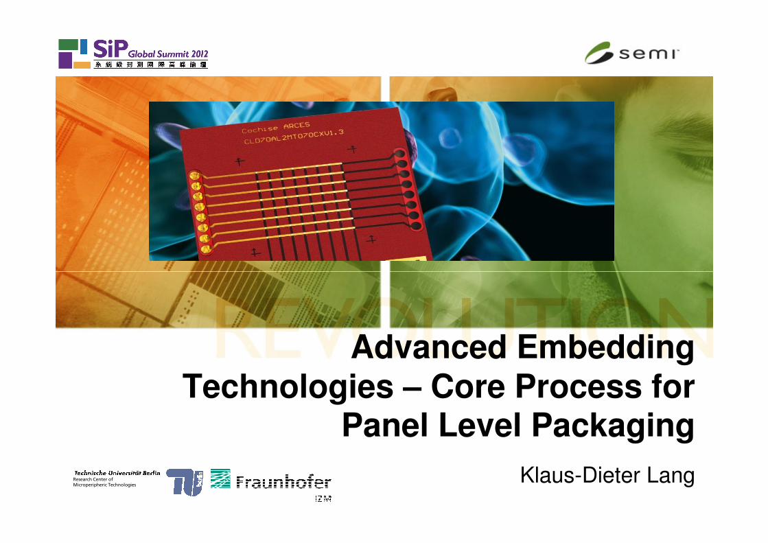
Advanced Embedding Technologies – Core Process for
Panel Level Packaging
Klaus-Dieter LangResearch Center ofMicroperipheric Technologies
Outline
� Introduction
� Future System Integration
� Embedding Technologies of Actives and Passives
Prof. Dr. Klaus-Dieter Lang
Semicon Taiwan;
Taipeh (07.09.2012)
Research Center ofMicroperipheric Technologies
� Embedding Technologies of Actives and Passives
� Modular Electronics based on Embedding Technologies
� Conclusions
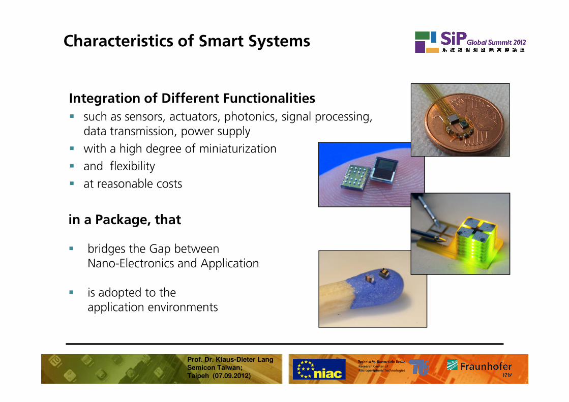
Integration of Different Functionalities
� such as sensors, actuators, photonics, signal processing, data transmission, power supply
� with a high degree of miniaturization
� and flexibility
� at reasonable costs
Characteristics of Smart Systems
Prof. Dr. Klaus-Dieter Lang
Semicon Taiwan;
Taipeh (07.09.2012)
Research Center ofMicroperipheric Technologies
in a Package, that
� bridges the Gap between Nano-Electronics and Application
� is adopted to theapplication environments
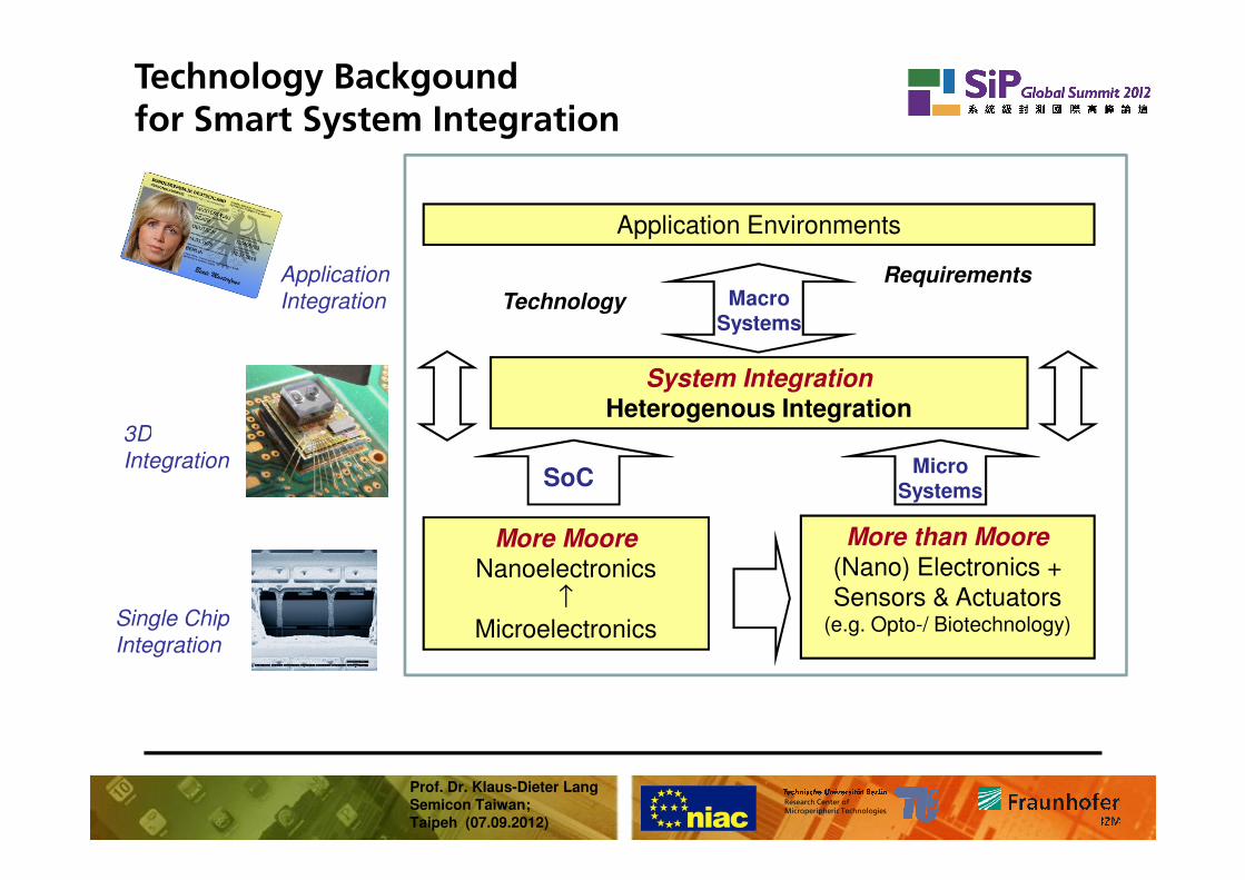
Application Environments
System IntegrationHeterogenous Integration
RequirementsTechnology
3D
Application
Integration MacroSystems
Technology Backgound for Smart System Integration
Prof. Dr. Klaus-Dieter Lang
Semicon Taiwan;
Taipeh (07.09.2012)
Research Center ofMicroperipheric Technologies
More MooreNanoelectronics
↑
Microelectronics
More than Moore(Nano) Electronics +Sensors & Actuators
(e.g. Opto-/ Biotechnology)
3D
Integration
Single Chip
Integration
SoCMicro
Systems
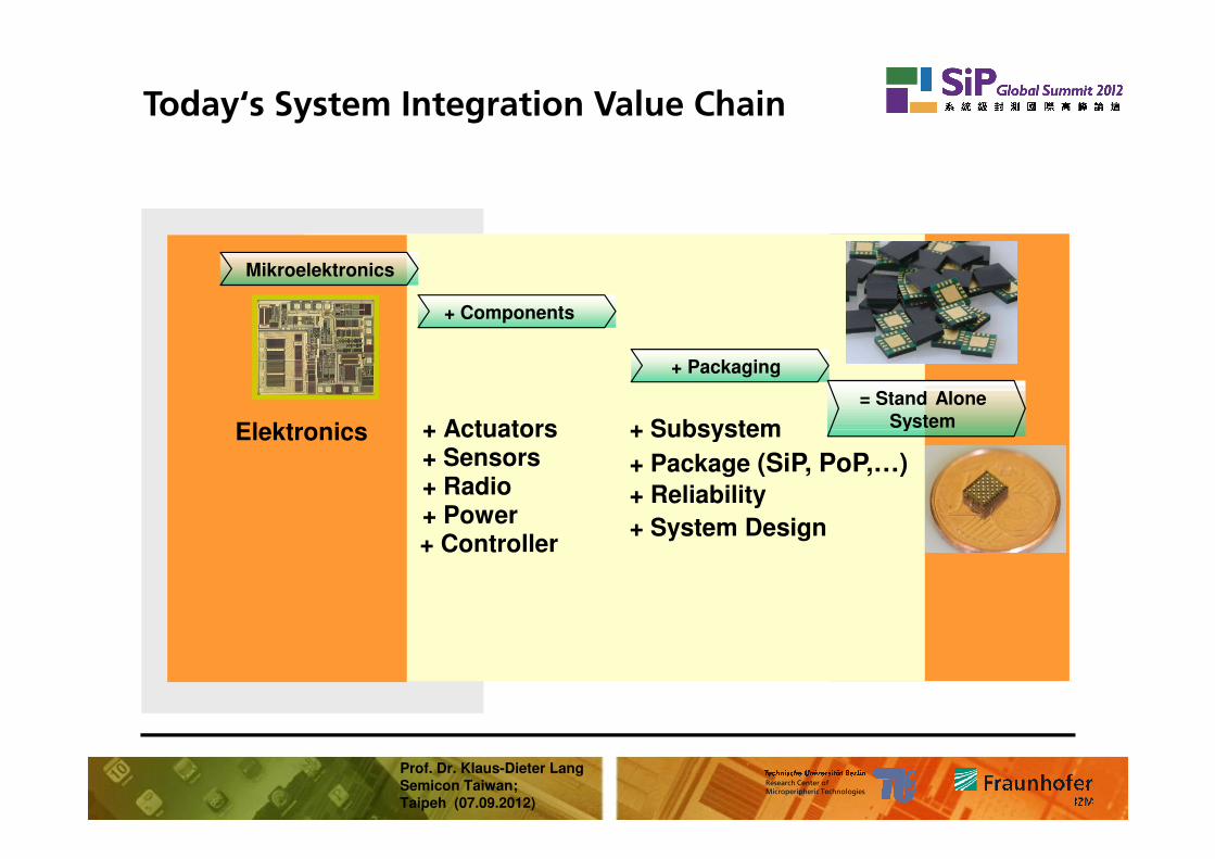
Today‘s System Integration Value Chain
Mikroelektronics
Elektronics
+ Components
+ Actuators + Subsystem
+ Packaging
= Stand Alone
System
Prof. Dr. Klaus-Dieter Lang
Semicon Taiwan;
Taipeh (07.09.2012)
Research Center ofMicroperipheric Technologies
m
Elektronics + Actuators+ Sensors+ Radio+ Power
+ Subsystem
+ Package (SiP, PoP,…) + Reliability
+ System Design
System
+ Controller
QFP ~ 5,5
13 mmBGA ~ 2
Package form factor
Package area
chip area
22 mm
Prof. Dr. Klaus-Dieter Lang
Semicon Taiwan;
Taipeh (07.09.2012)
Research Center ofMicroperipheric Technologies
9,34 mm
FCoB/ WLP fan in = 1
CSP < 1,2
Stacks: could become <1 and
external I/O no may be reduced
3D allows further density increase
PoP/SiP
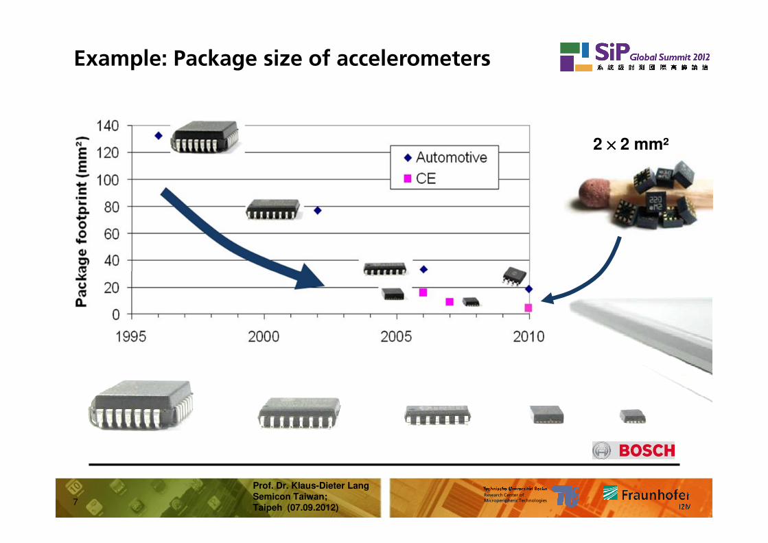
Bosch Sensors
2 ×××× 2 mm²
Example: Package size of accelerometers
Prof. Dr. Klaus-Dieter Lang
Semicon Taiwan;
Taipeh (07.09.2012)
Research Center ofMicroperipheric Technologies7
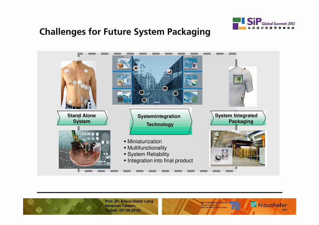
Challenges for Future System Packaging
Das Bild kann nicht angezeigt werden. Dieser Computer verfügt möglicherweise über zu wenig Arbeitsspeicher, um das Bild zu öffnen, oder das Bild ist beschädigt. Starten Sie den Computer neu, und öffnen Sie dann erneut die Datei. Wenn weiterhin das rote x angezeigt wird, müssen Sie das Bild möglicherweise löschen und dann erneut einfügen.
Prof. Dr. Klaus-Dieter Lang
Semicon Taiwan;
Taipeh (07.09.2012)
Research Center ofMicroperipheric Technologies
nm
Stand AloneSystem
Systemintegration
Technology
System Integrated Packaging
� Miniaturization� Multifunctionality� System Reliability� Integration into final product
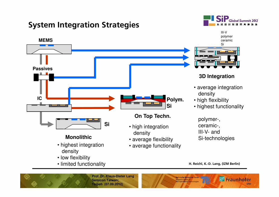
3D Integration
IC
Passives
MEMS
• average integration
density
• high flexibilityPolym.
III-V
polymer
ceramic
Si
System Integration Strategies
Prof. Dr. Klaus-Dieter Lang
Semicon Taiwan;
Taipeh (07.09.2012)
Research Center ofMicroperipheric Technologies
IC
Monolithic
On Top Techn.
• high integration
density
• average flexibility
• average functionality• highest integration
density
• low flexibility
• limited functionality
• high flexibility
• highest functionality
polymer-,
ceramic-,
III-V- and
Si-technologies
Si
Polym.
Si
H. Reichl, K.-D. Lang, (IZM Berlin)
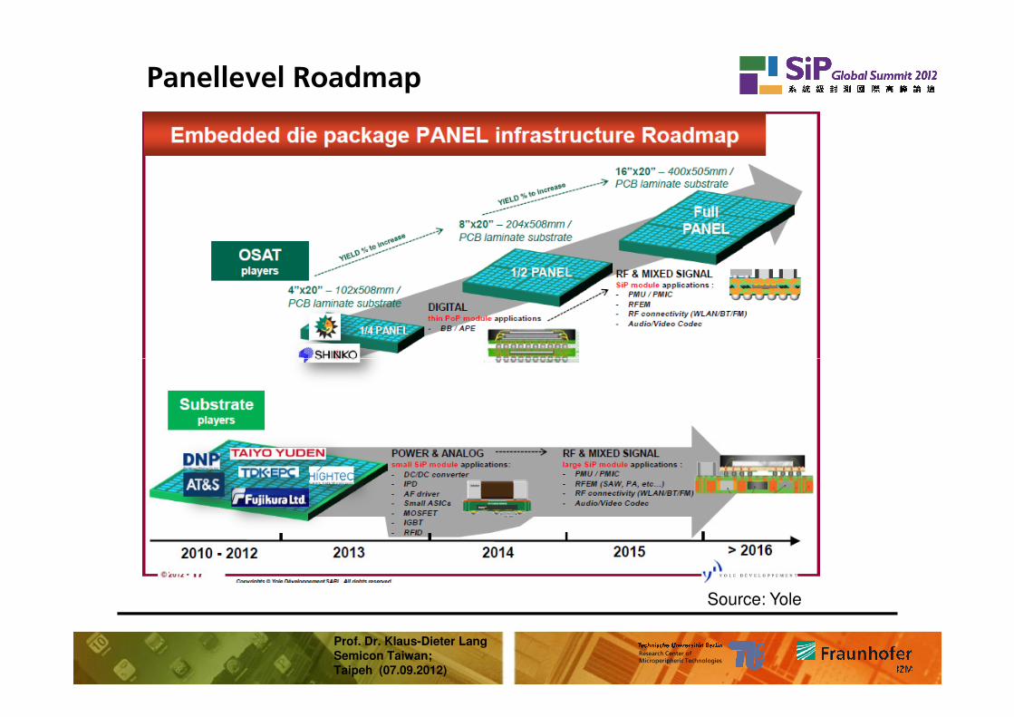
Panellevel Roadmap
Prof. Dr. Klaus-Dieter Lang
Semicon Taiwan;
Taipeh (07.09.2012)
Research Center ofMicroperipheric Technologies
Source: Yole
Outline
� Introduction
� Future System Integration
� Embedding Technologies of Actives and Passives
Prof. Dr. Klaus-Dieter Lang
Semicon Taiwan;
Taipeh (07.09.2012)
Research Center ofMicroperipheric Technologies
� Embedding Technologies of Actives and Passives
� Modular Electronics based on Embedding Technologies
� Conclusions
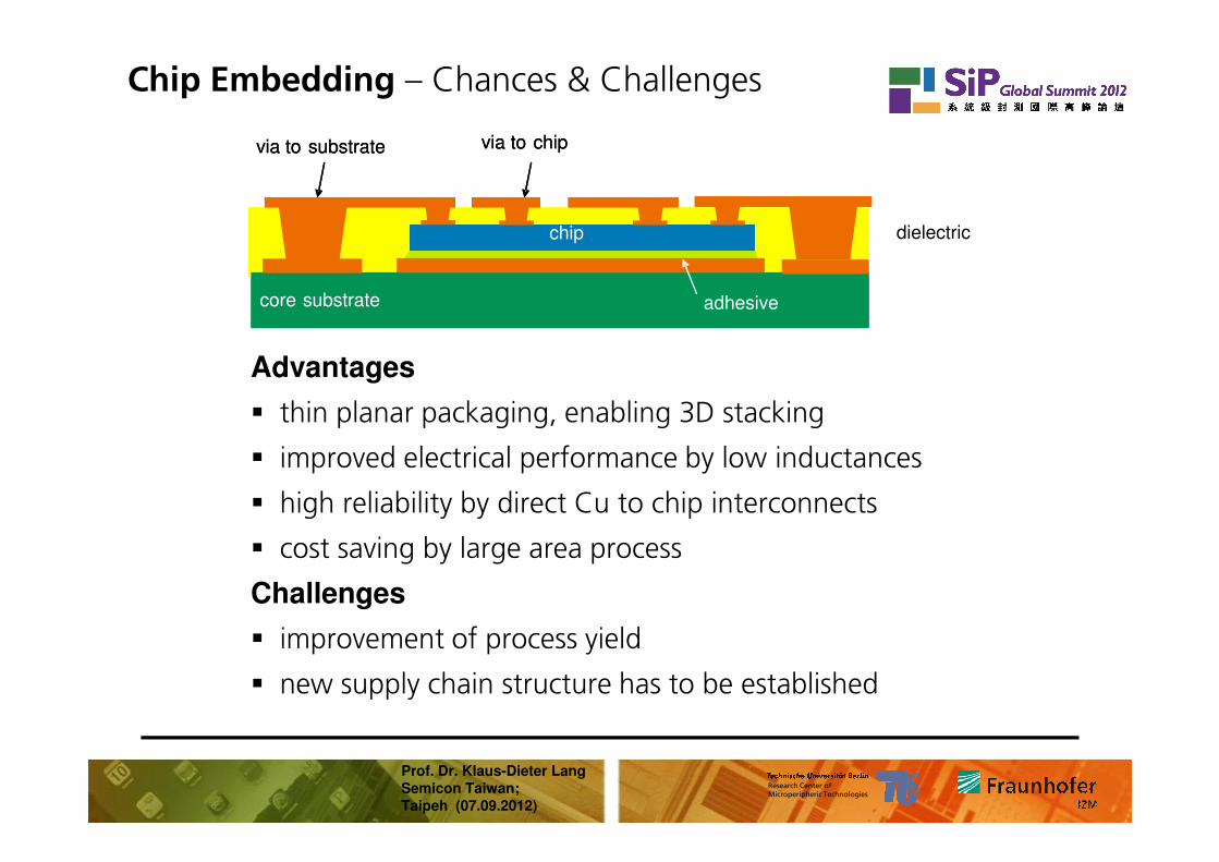
Chip Embedding – Chances & Challenges
via to substrate via to chip
chip
core substrate adhesive
via to substrate via to chip
chip
core substrate adhesive
dielectric
Advantages
� thin planar packaging, enabling 3D stacking
Prof. Dr. Klaus-Dieter Lang
Semicon Taiwan;
Taipeh (07.09.2012)
Research Center ofMicroperipheric Technologies
� improved electrical performance by low inductances
� high reliability by direct Cu to chip interconnects
� cost saving by large area process
Challenges
� improvement of process yield
� new supply chain structure has to be established
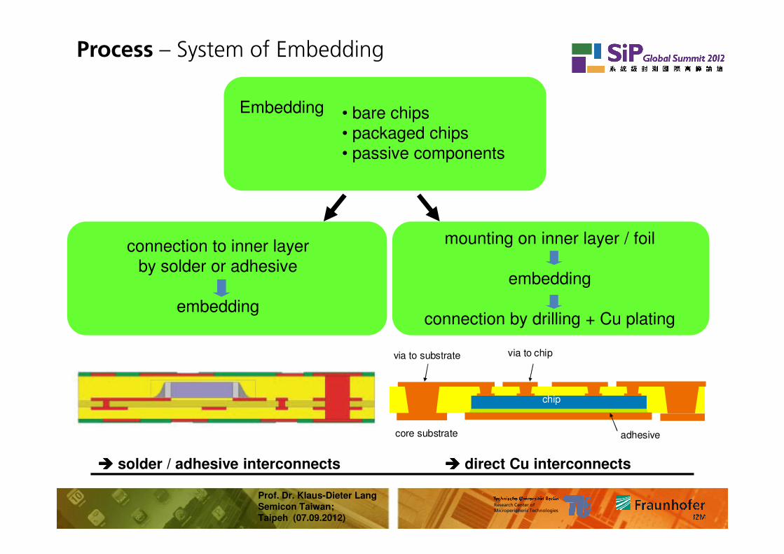
Process – System of Embedding
Embedding • bare chips• packaged chips• passive components
connection to inner layerby solder or adhesive
mounting on inner layer / foil
embedding
Prof. Dr. Klaus-Dieter Lang
Semicon Taiwan;
Taipeh (07.09.2012)
Research Center ofMicroperipheric Technologies
���� solder / adhesive interconnects ���� direct Cu interconnects
via to substrate via to chip
chip
core substrate adhesive
embedding
embedding
connection by drilling + Cu plating
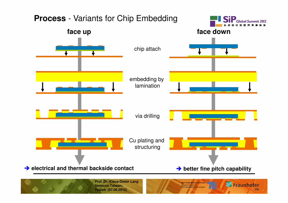
Process - Variants for Chip Embedding
face down
chip attach
embedding by
lamination
face up
Prof. Dr. Klaus-Dieter Lang
Semicon Taiwan;
Taipeh (07.09.2012)
Research Center ofMicroperipheric Technologies
� better fine pitch capability
via drilling
Cu plating and
structuring
� electrical and thermal backside contact
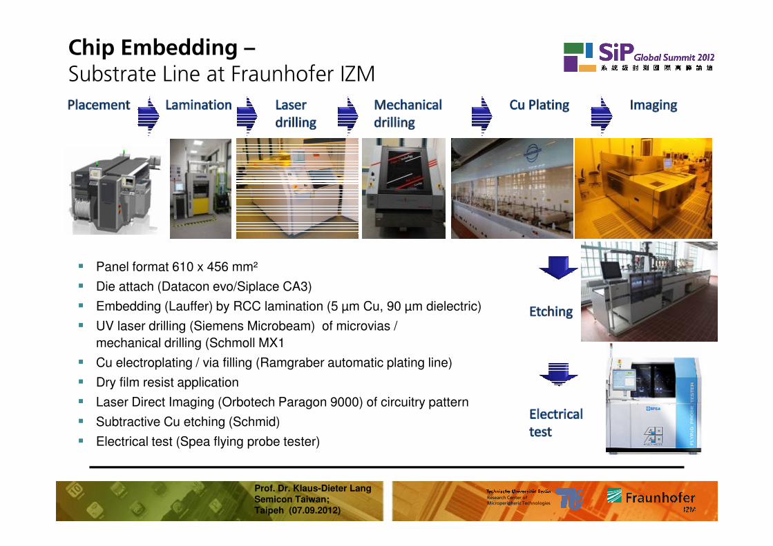
Chip Embedding –Substrate Line at Fraunhofer IZM
� Panel format 610 x 456 mm²
Prof. Dr. Klaus-Dieter Lang
Semicon Taiwan;
Taipeh (07.09.2012)
Research Center ofMicroperipheric Technologies
� Panel format 610 x 456 mm²
� Die attach (Datacon evo/Siplace CA3)
� Embedding (Lauffer) by RCC lamination (5 µm Cu, 90 µm dielectric)
� UV laser drilling (Siemens Microbeam) of microvias /
mechanical drilling (Schmoll MX1
� Cu electroplating / via filling (Ramgraber automatic plating line)
� Dry film resist application
� Laser Direct Imaging (Orbotech Paragon 9000) of circuitry pattern
� Subtractive Cu etching (Schmid)
� Electrical test (Spea flying probe tester)
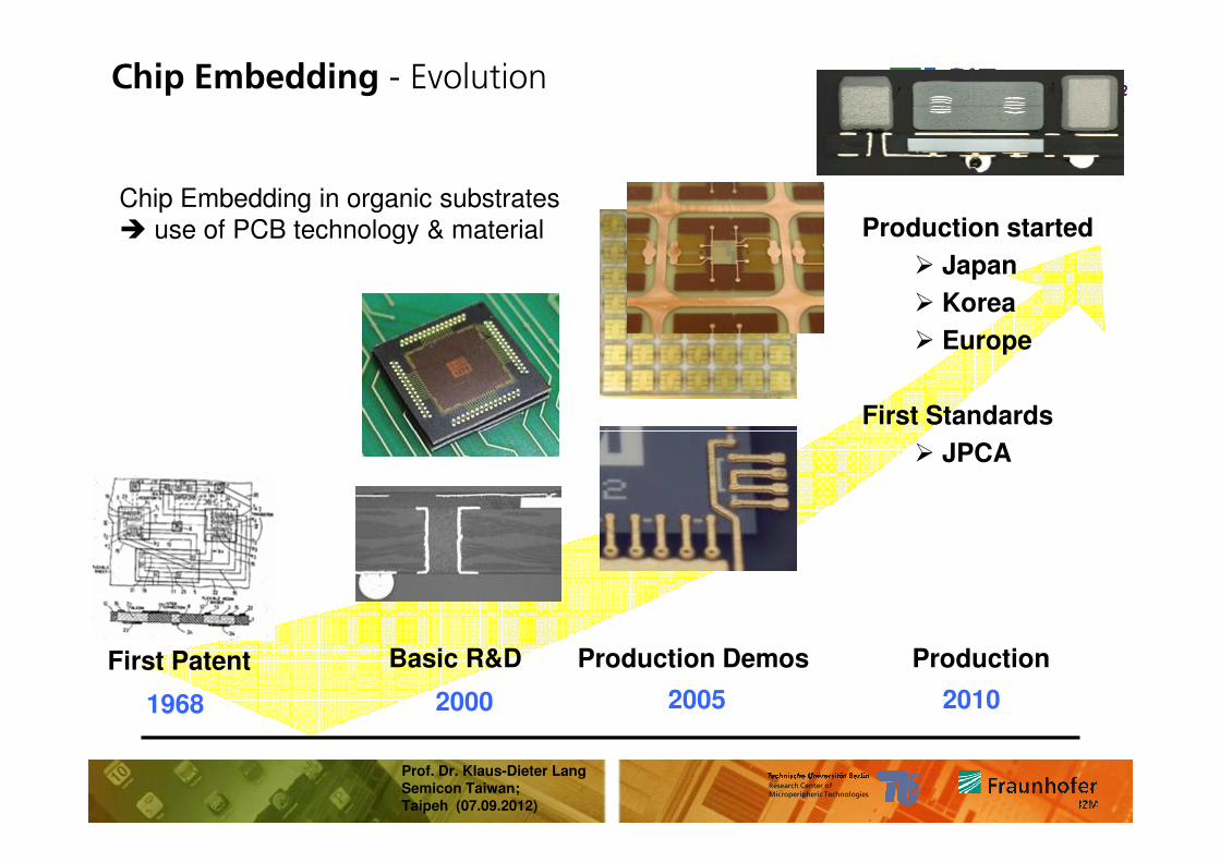
Chip Embedding - Evolution
Production started
� Japan
� Korea
� Europe
First Standards
Chip Embedding in organic substrates� use of PCB technology & material
Prof. Dr. Klaus-Dieter Lang
Semicon Taiwan;
Taipeh (07.09.2012)
Research Center ofMicroperipheric Technologies
First Patent
1968 2000
Basic R&D
2005
Production Demos
2010
Production
� JPCA
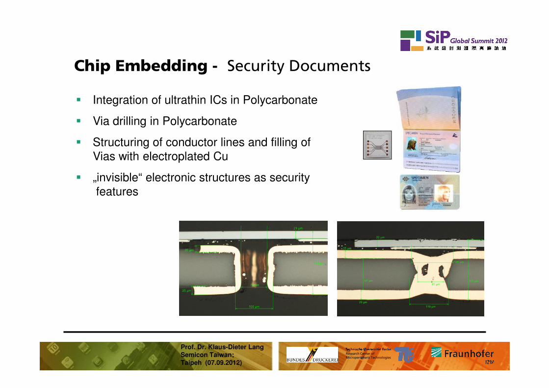
Chip Embedding - Security Documents
� Integration of ultrathin ICs in Polycarbonate
� Via drilling in Polycarbonate
� Structuring of conductor lines and filling ofVias with electroplated Cu
� „invisible“ electronic structures as securityfeatures
Prof. Dr. Klaus-Dieter Lang
Semicon Taiwan;
Taipeh (07.09.2012)
Research Center ofMicroperipheric Technologies
features
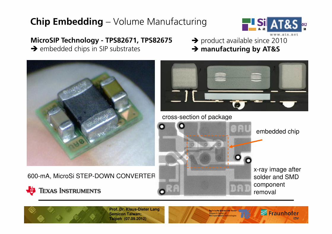
MicroSIP Technology - TPS82671, TPS82675� embedded chips in SIP substrates
cross-section of package
� product available since 2010� manufacturing by AT&S
Chip Embedding – Volume Manufacturing
Prof. Dr. Klaus-Dieter Lang
Semicon Taiwan;
Taipeh (07.09.2012)
Research Center ofMicroperipheric Technologies
600-mA, MicroSi STEP-DOWN CONVERTER)
cross-section of package
embedded chip
x-ray image after
solder and SMD
component
removal
Outline
� Introduction
� Future System Integration
� Embedding Technologies of Actives and Passives
Prof. Dr. Klaus-Dieter Lang
Semicon Taiwan;
Taipeh (07.09.2012)
Research Center ofMicroperipheric Technologies
� Embedding Technologies of Actives and Passives
� Modular Electronics based on Embedding Technologies
� Conclusions
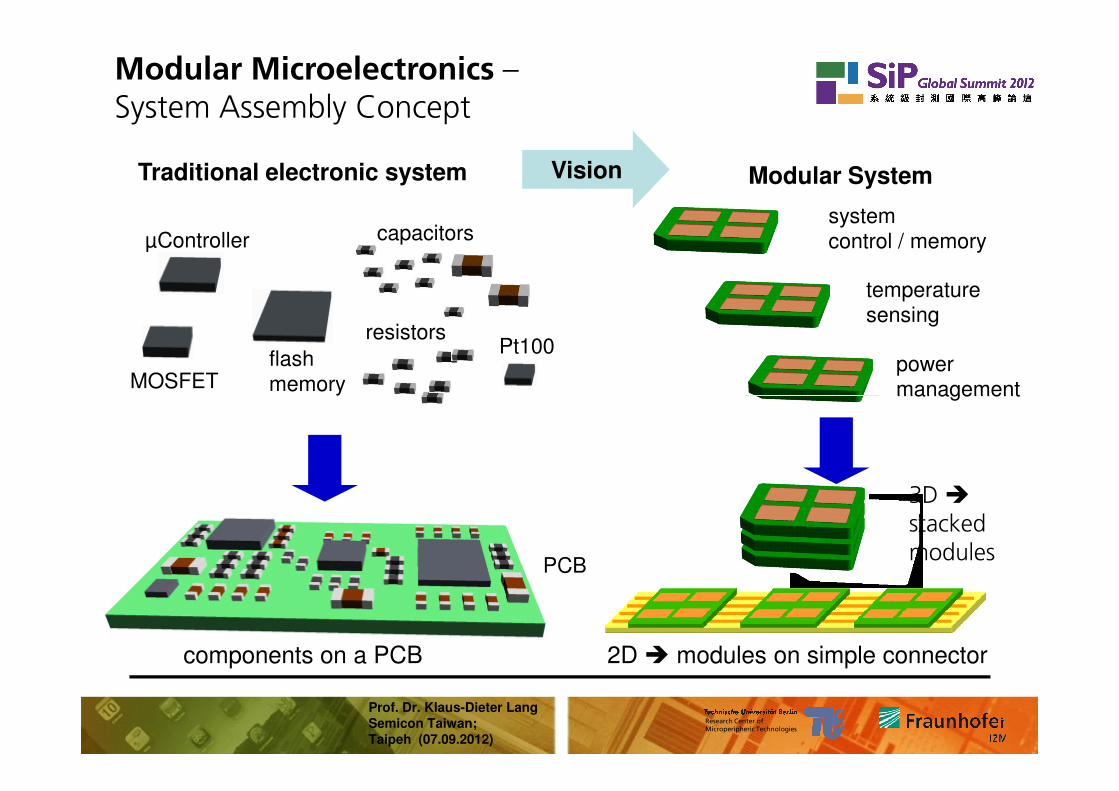
Modular Microelectronics –System Assembly Concept
Modular System
system control / memory
temperature sensing
power management
Traditional electronic system
resistors
µController
MOSFETflash memory
capacitors
Pt100
Vision
Prof. Dr. Klaus-Dieter Lang
Semicon Taiwan;
Taipeh (07.09.2012)
Research Center ofMicroperipheric Technologies
managementmemory
PCB
components on a PCB
3D �stacked modules
2D � modules on simple connector
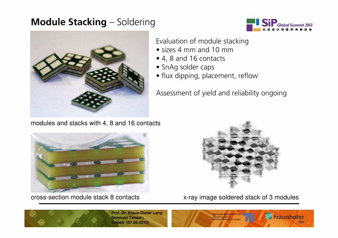
Module Stacking – Soldering
Evaluation of module stacking• sizes 4 mm and 10 mm• 4, 8 and 16 contacts• SnAg solder caps• flux dipping, placement, reflow
Assessment of yield and reliability ongoing
Prof. Dr. Klaus-Dieter Lang
Semicon Taiwan;
Taipeh (07.09.2012)
Research Center ofMicroperipheric Technologies
modules and stacks with 4, 8 and 16 contacts
cross-section module stack 8 contacts x-ray image soldered stack of 3 modules
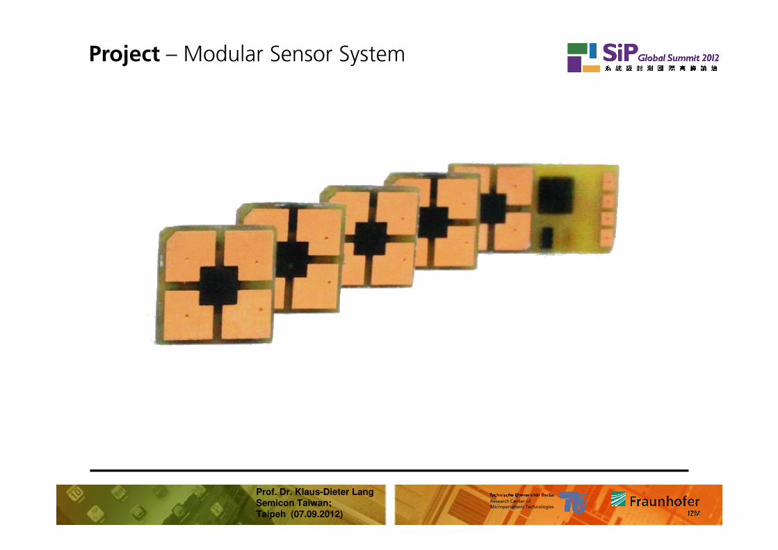
Project – Modular Sensor System
Prof. Dr. Klaus-Dieter Lang
Semicon Taiwan;
Taipeh (07.09.2012)
Research Center ofMicroperipheric Technologies
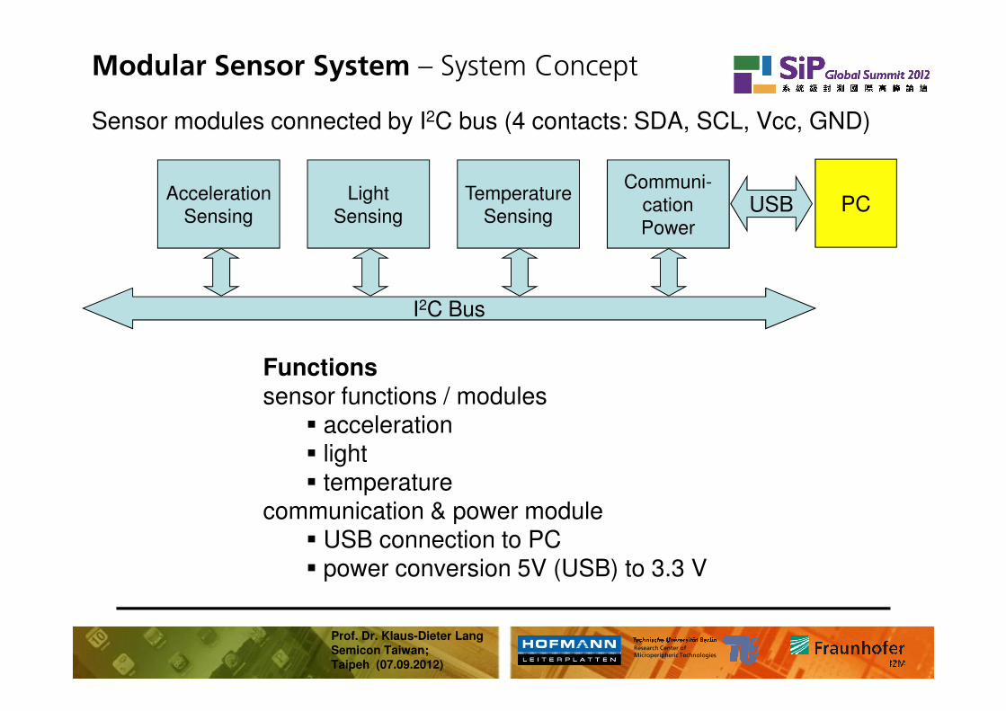
Modular Sensor System – System Concept
I2C Bus
Acceleration
Sensing
Light
Sensing
Temperature
Sensing
Communi-
cation
PowerUSB PC
Functions
Sensor modules connected by I2C bus (4 contacts: SDA, SCL, Vcc, GND)
Prof. Dr. Klaus-Dieter Lang
Semicon Taiwan;
Taipeh (07.09.2012)
Research Center ofMicroperipheric Technologies
Functionssensor functions / modules
� acceleration� light� temperature
communication & power module� USB connection to PC� power conversion 5V (USB) to 3.3 V
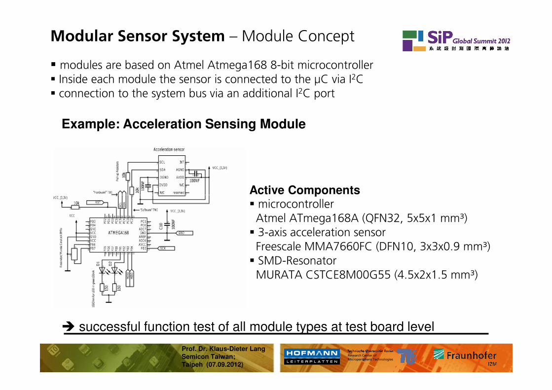
Modular Sensor System – Module Concept
Active Components
� modules are based on Atmel Atmega168 8-bit microcontroller� Inside each module the sensor is connected to the µC via I2C� connection to the system bus via an additional I2C port
Example: Acceleration Sensing Module
Prof. Dr. Klaus-Dieter Lang
Semicon Taiwan;
Taipeh (07.09.2012)
Research Center ofMicroperipheric Technologies
Active Components� microcontrollerAtmel ATmega168A (QFN32, 5x5x1 mm³)
� 3-axis acceleration sensor Freescale MMA7660FC (DFN10, 3x3x0.9 mm³)
� SMD-Resonator MURATA CSTCE8M00G55 (4.5x2x1.5 mm³)
� successful function test of all module types at test board level
circuit diagram
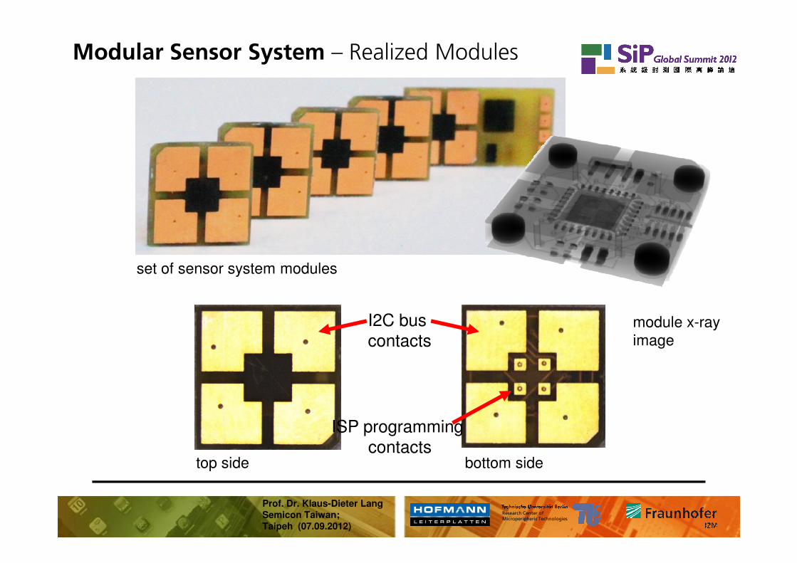
Modular Sensor System – Realized Modules
set of sensor system modules
Prof. Dr. Klaus-Dieter Lang
Semicon Taiwan;
Taipeh (07.09.2012)
Research Center ofMicroperipheric Technologies
top side bottom side
ISP programming contacts
I2C bus contacts
module x-ray
image
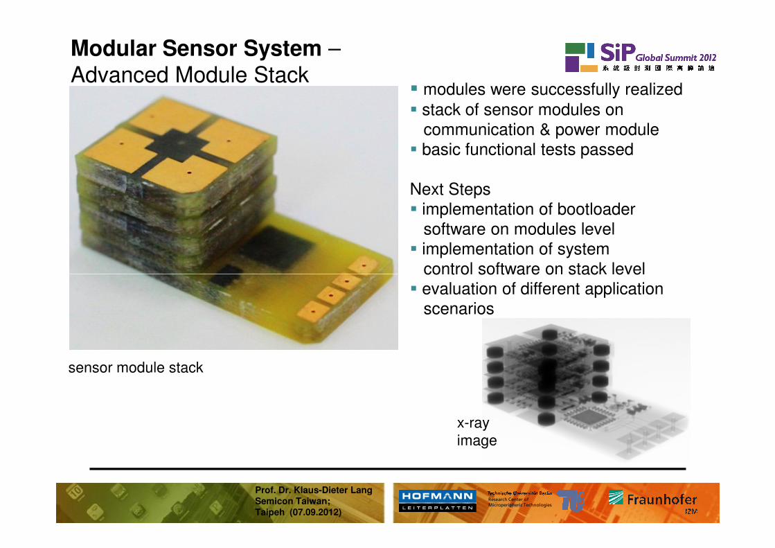
Modular Sensor System –Advanced Module Stack
� modules were successfully realized
� stack of sensor modules on communication & power module
� basic functional tests passed
Next Steps� implementation of bootloader
software on modules level� implementation of system
control software on stack level
Prof. Dr. Klaus-Dieter Lang
Semicon Taiwan;
Taipeh (07.09.2012)
Research Center ofMicroperipheric Technologies
x-ray
image
sensor module stack
control software on stack level� evaluation of different application
scenarios
Outline
� Introduction
� Future System Integration
� Embedding Technologies of Actives and Passives
Prof. Dr. Klaus-Dieter Lang
Semicon Taiwan;
Taipeh (07.09.2012)
Research Center ofMicroperipheric Technologies
� Embedding Technologies of Actives and Passives
� Modular Electronics based on Embedding Technologies
� Conclusions
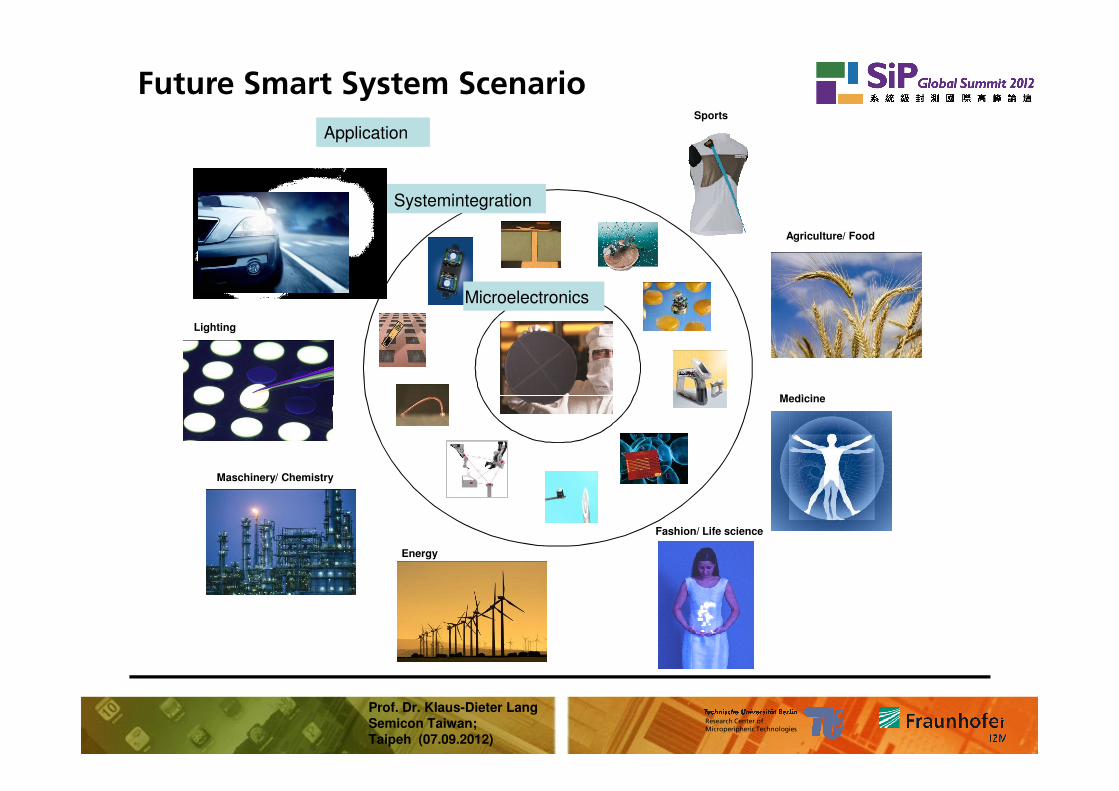
Application
Traffic
Sports
Medicine
Lighting
Agriculture/ Food
Microelectronics
Systemintegration
Future Smart System Scenario
Prof. Dr. Klaus-Dieter Lang
Semicon Taiwan;
Taipeh (07.09.2012)
Research Center ofMicroperipheric Technologies
Maschinery/ Chemistry
Medicine
Energy
Fashion/ Life science
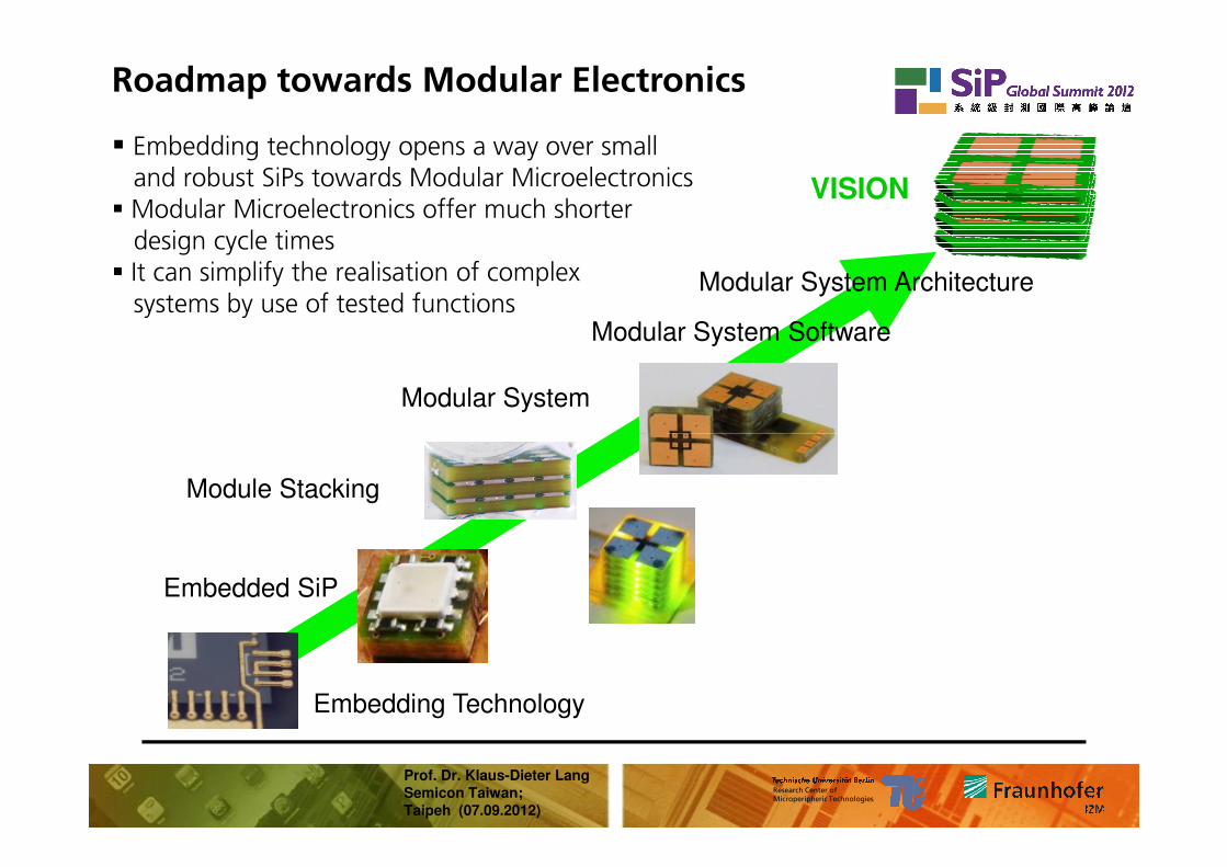
Roadmap towards Modular Electronics
Modular System
VISION
Modular System Software
Modular System Architecture
� Embedding technology opens a way over small and robust SiPs towards Modular Microelectronics
� Modular Microelectronics offer much shorter design cycle times
� It can simplify the realisation of complex systems by use of tested functions
Prof. Dr. Klaus-Dieter Lang
Semicon Taiwan;
Taipeh (07.09.2012)
Research Center ofMicroperipheric Technologies
Embedding Technology
Module Stacking
Embedded SiP
� Improvement of cooperation between established PCB technologies andEmbedding in production areas
� Faster implementation of advanced assembly and packaging(e.g. 3D Integration, Panel Level Packaging)
� Materials development to optimize integration of embedding processesinto different application environments (e.g. innovative polymer substrates)
� Known Good Die handling for ICs , MEMS, Optic components, etc
Tasks and Challenges
Prof. Dr. Klaus-Dieter Lang
Semicon Taiwan;
Taipeh (07.09.2012)
Research Center ofMicroperipheric Technologies
� Known Good Die handling for ICs , MEMS, Optic components, etc
� Interaction of design, technology and reliability at a very early stage of development will be essential for the product success. Especially models andsimulations for that have to be allocated.
� Interconnection processes and interfaces at the border from micro to nanohave to be understood better
� System test methodologies and new manufacturing standards have to be implemented
Fraunhofer-InstitutZuverlässigkeit und Mikrointegration IZMGustav-Meyer-Allee 2513355 Berlin
Kontakt: Prof. Dr. Klaus-Dieter LangTel: +49 30 46403-179E-Mail [email protected]
Web: www.izm.fraunhofer.de
Prof. Dr. Klaus-Dieter Lang
Semicon Taiwan;
Taipeh (07.09.2012)
Research Center ofMicroperipheric Technologies
Thank you for your Attention


