40
Altera Quartus II Tutorial CSE140L – WI06 TA: Jianhua Liu CSE Dept. UCSD

Altera Quartus II Tutorial
CSE140L – WI06TA: Jianhua Liu
CSE Dept. UCSD

Altera Quartus II
The Quartus II development software provides a complete design environmentfor FPGA designs. Design entry using schematics, block diagrams, VHDL, and Verilog HDL . Design analysis and synthesis, fitting, assembling, timing analysis, simulation.

Altera Quartus II
Design flow• Design entry
• Analysis andsynthesis
• Fitting
• Assembling
• Timing analysis
• Simulation
Quartus II• HDL editor
• Block diagram,schematic editor
• Compiler tool
• Compilation report
• Timing closure floorplan
• Simulator tool
• Waveform editor

Tutorial Outline
Open Quartus II and pick a device.Build a full adder. (Block/Schematic)
Add componentsAdd portsAdd connections (single wire connection)
Build a 4-bit adder.Create a block for full adderUse conduit and port mapping
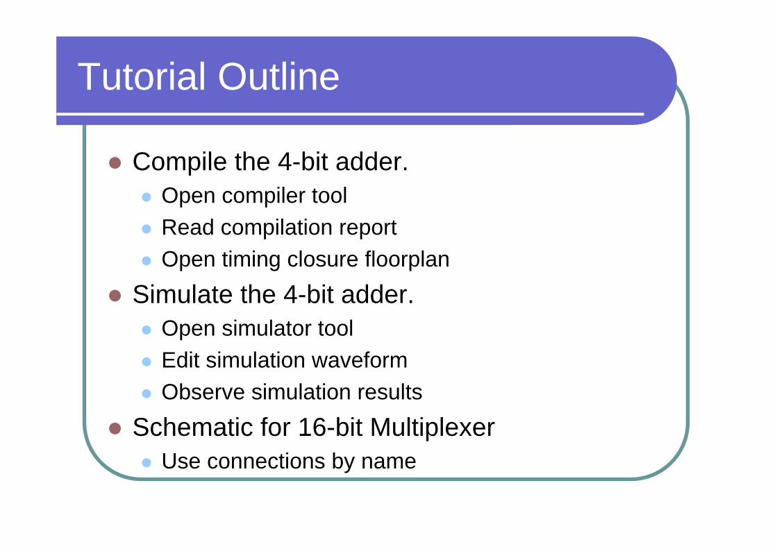
Tutorial Outline
Compile the 4-bit adder.Open compiler toolRead compilation reportOpen timing closure floorplan
Simulate the 4-bit adder.Open simulator toolEdit simulation waveformObserve simulation results
Schematic for 16-bit MultiplexerUse connections by name
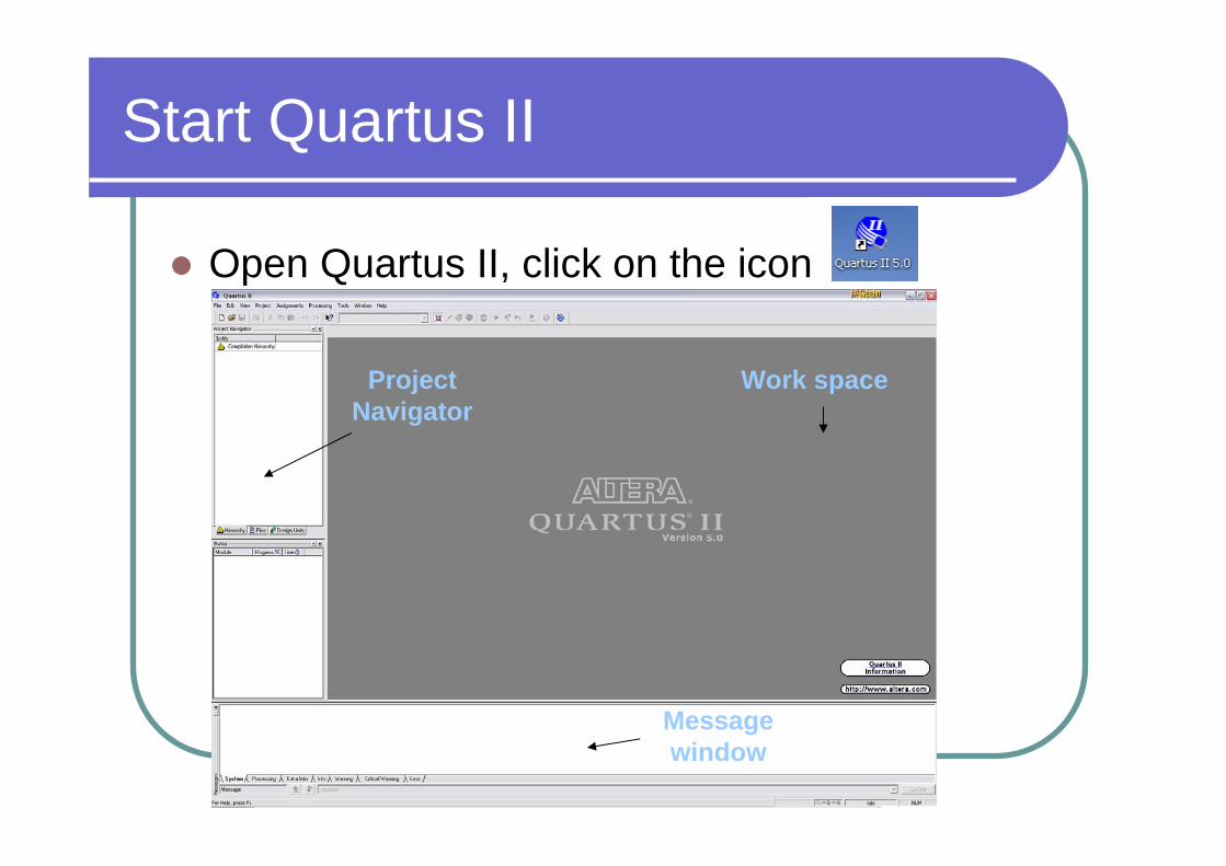
Start Quartus II
Open Quartus II, click on the icon
Work spaceProject Navigator
Message window
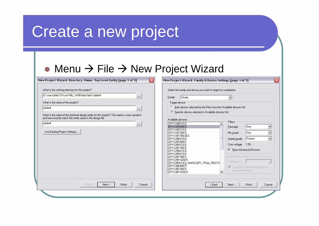
Create a new project
Menu File New Project Wizard

Build a full adder
Menu File NewCreate a Block Diagram/Schematic FileMenu File Save As: fadder.bdf
LibraryNew BlockSingle WireBusConduit
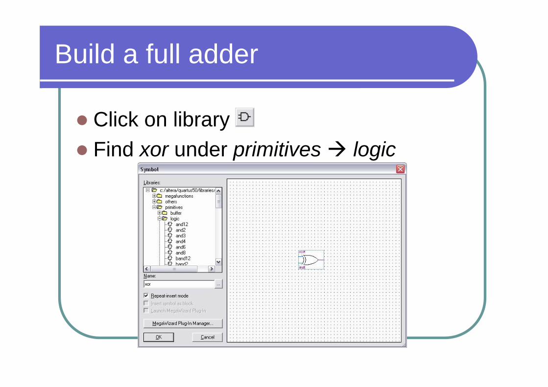
Build a full adder
Click on libraryFind xor under primitives logic

Build a full adder
Place two xor, two and2 and one or2.

Build a full adder
Find input and output under primitives pin, and place three input and two outputDouble click on each pin, to change pin name.
Build a full adder
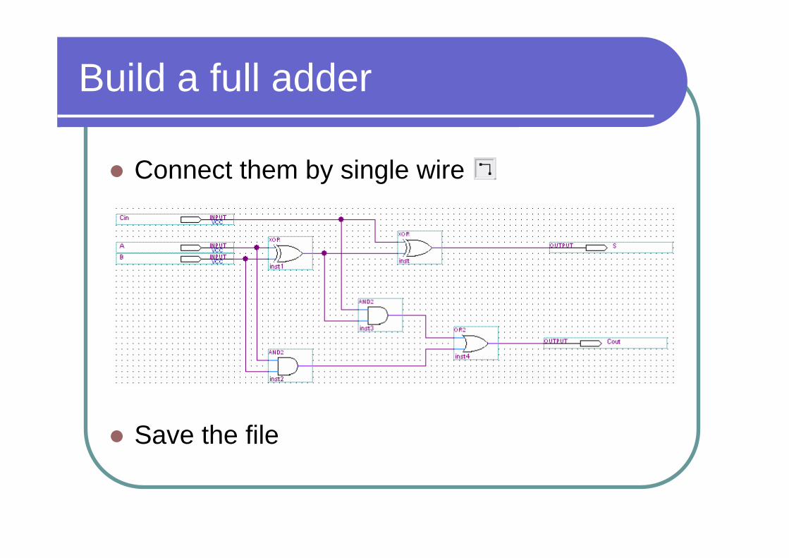
Connect them by single wire
Save the file

Questions

Build a 4-bit adder
Menu File NewCreate a Block Diagram/Schematic FileMenu File Save As: adder4.bdfClick on new block , and draw a block.Double click on the block name, change it to fadder

Build a 4-bit adder
Right click on the block, and select Block Properties in the pop-up menu. In the tag I/Os, add the following ports:
Build a 4-bit adder
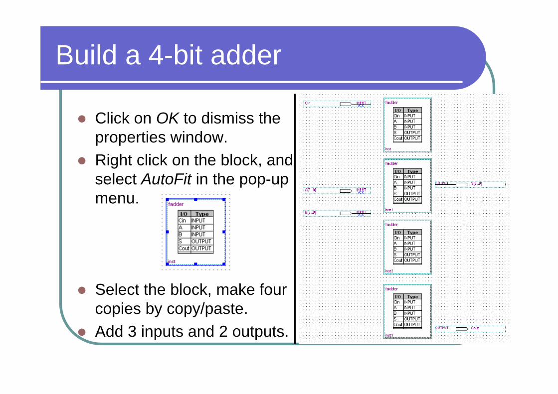
Click on OK to dismiss the properties window.Right click on the block, and select AutoFit in the pop-up menu.
Select the block, make four copies by copy/paste.Add 3 inputs and 2 outputs.

Build a 4-bit adder
Use conduit tool to connect each fadder to inputs and outputs. Conduit can stop at any point on a block border.
Build a 4-bit adder
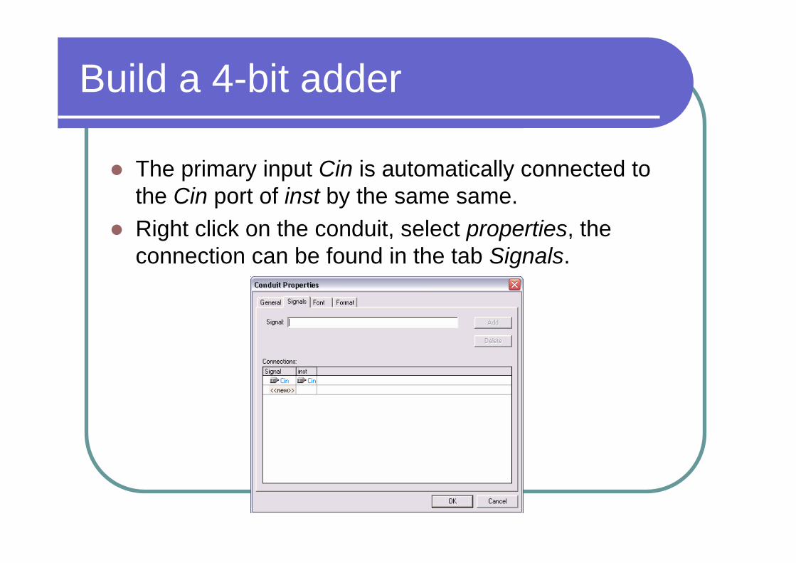
The primary input Cin is automatically connected to the Cin port of inst by the same same. Right click on the conduit, select properties, the connection can be found in the tab Signals.

Build a 4-bit adder
For A[3..0], B[3..0] and S[3..0], port mapping should be manually defined. Edit the signals property for A[3..0] like this:
Build a 4-bit adder
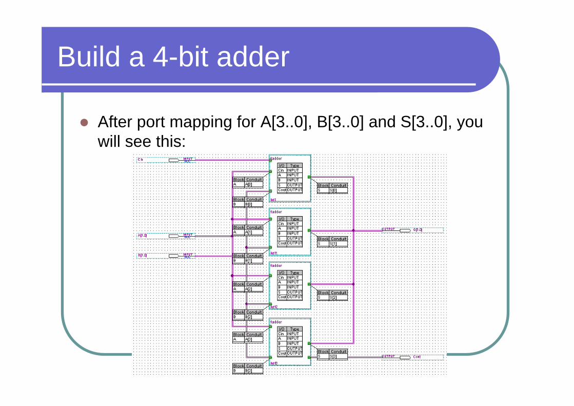
After port mapping for A[3..0], B[3..0] and S[3..0], you will see this:

Build a 4-bit adder
Place single wires for carry signals.
Build a 4-bit adder
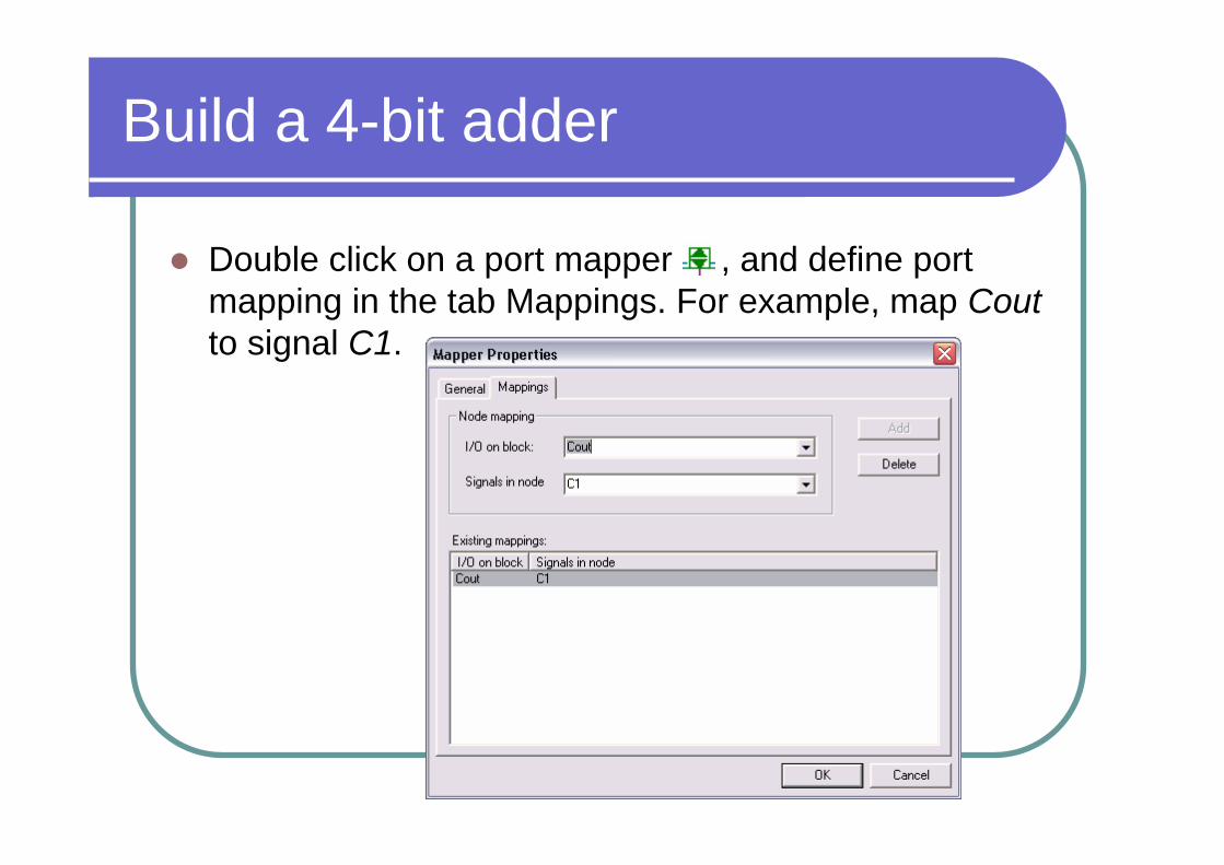
Double click on a port mapper , and define port mapping in the tab Mappings. For example, map Coutto signal C1.
Build a 4-bit adder
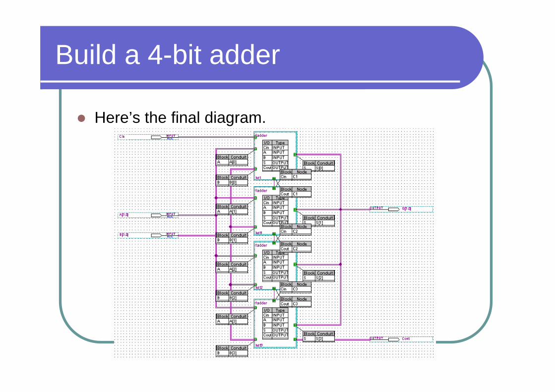
Here’s the final diagram.

Questions
Compile the design
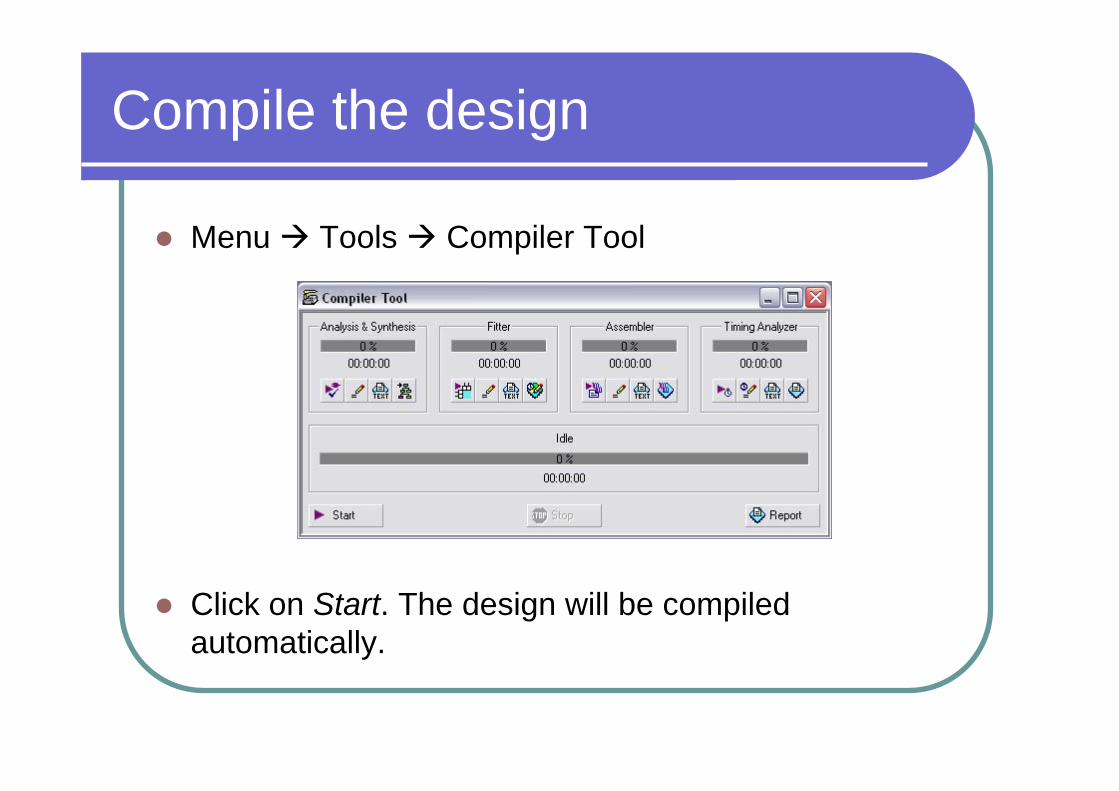
Menu Tools Compiler Tool
Click on Start. The design will be compiled automatically.

Compile the design
Click on Report button after compilation.

Compile the design
Worst delay can be found in Timing Analyzer report

Compile the design
Select the worst delay, right click on it, and select locate in the pop-up menu Locate in Timing Closure Floorplan. You can see the design implementation in the FPGA device.
Simulate the design
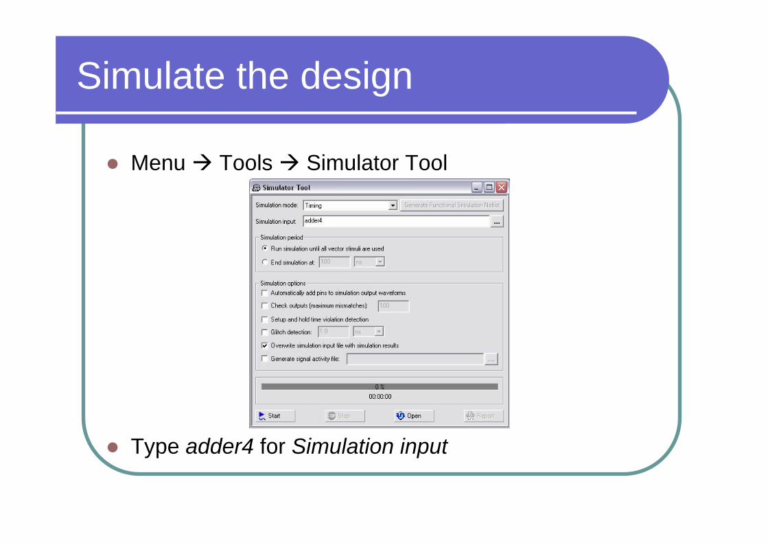
Menu Tools Simulator Tool
Type adder4 for Simulation input

Simulate the design
Click on Open button , and save the file as adder4.vwf
Signals Waveforms

Simulate the design
Double click on signals area, and click the button Node FinderList all the pins and select the primary inputs and outputs, then click OK.

Simulate the design
To change the value of each input, right click on the input and select value in the pop-up menu.
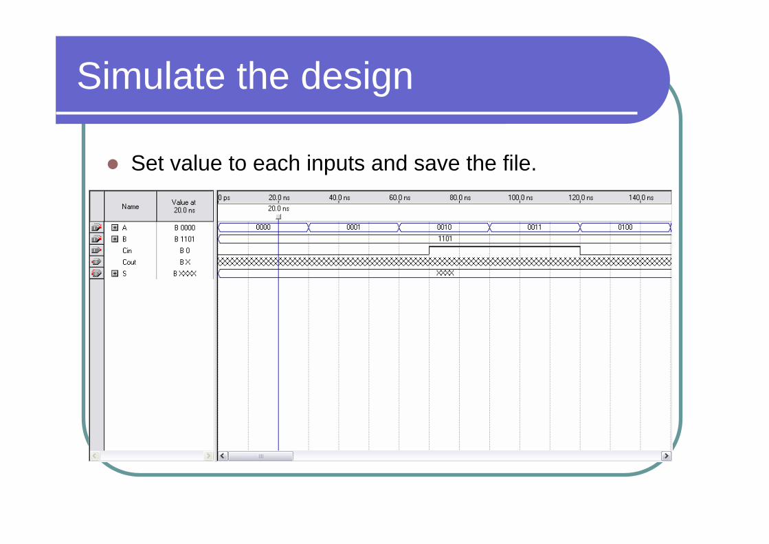
Simulate the design
Set value to each inputs and save the file.

Simulate the design
Go back to the simulator tool, and click on the button Start . adder4.vwf will be updated after the simulation.

Simulate the design
The correctness of the design is verified, and the worst delay can be identified.

Questions

Schematic for 16-bit Multiplexer
The schematic diagram of a 4-bit Multiplexer. Note that the wires connected by name.

Schematic for 16-bit Multiplexer
To name a wire/bus, right click the wire/bus, select properties in the pop-up menu, and then fill in the name.

Schematic for 16-bit Multiplexer
The schematic diagram of a 16-bit Multiplexer.

Questions


