98
AMD SB600 BIOS Developer’s Guide (Public Version) Technical Reference Manual Rev. 3.00 P/N: 46157_sb600_bdg_pub_3.00 ©2008 Advanced Micro Devices, Inc.

AMD SB600 BIOS Developer’s Guide (Public Version)
Technical Reference Manual Rev. 3.00
P/N: 46157_sb600_bdg_pub_3.00
©2008 Advanced Micro Devices, Inc.

Trademarks AMD, the AMD Arrow, ATI, the ATI logo, Radeon, Mobility Radeon, AMD Athlon, Sempron, Turion and combinations thereof are trademarks of Advanced Micro Devices, Inc. HyperTransport is a licensed trademark of the HyperTransport Technology Consortium.
Microsoft and Windows are registered trademarks of Microsoft Corporation.
Other product names used in this publication are for identification purposes only and may be trademarks of their respective companies.
Disclaimer
The contents of this document are provided in connection with Advanced Micro Devices, Inc. ("AMD") products. AMD makes no representations or warranties with respect to the accuracy or completeness of the contents of this publication and reserves the right to make changes to specifications and product descriptions at any time without notice. No license, whether express, implied, arising by estoppel, or otherwise, to any intellectual property rights are granted by this publication. Except as set forth in AMD's Standard Terms and Conditions of Sale, AMD assumes no liability whatsoever, and disclaims any express or implied warranty, relating to its products including, but not limited to, the implied warranty of merchantability, fitness for a particular purpose, or infringement of any intellectual property right.
AMD's products are not designed, intended, authorized or warranted for use as components in systems intended for surgical implant into the body, or in other applications intended to support or sustain life, or in any other application in which the failure of AMD's product could create a situation where personal injury, death, or severe property or environmental damage may occur. AMD reserves the right to discontinue or make changes to its products at any time without notice.
.

© 2008 Advanced Micro Devices Inc. Table of ContentsAMD SB600 BIOS Developer’s Guide (Public Version) Proprietary Page 3
Table of Contents
1 Introduction ................................................................................................................. 7 1.1 About This Manual........................................................................................................................ 7 1.2 Overview ....................................................................................................................................... 7 1.3 PCI Internal Devices ................................................................................................................... 10
2 SB600 Programming Architecture .......................................................................... 12 2.1 PCI Devices and Functions ......................................................................................................... 12 2.2 I/O Map ....................................................................................................................................... 13
2.2.1 Fixed I/O Address Ranges ...................................................................................................................13 2.2.1.1 Fixed I/O Address Ranges – SB600 Proprietary Ports ................................................................13
2.2.2 Variable I/O Decode Ranges ...............................................................................................................13 2.3 Memory Map............................................................................................................................... 14
3 SB600 Early-POST Initialization............................................................................. 15 3.1 512K/1M ROM Enable ............................................................................................................... 15
3.1.1 PCI ROM.............................................................................................................................................15 3.1.2 LPC ROM............................................................................................................................................15 3.1.3 LPC ROM Read/Write Protect ............................................................................................................15 3.1.4 SPI ROM controller.............................................................................................................................16
3.2 Real Time Clock (RTC) .............................................................................................................. 17 3.2.1 RTC Access .........................................................................................................................................17
3.2.1.1 Special Locked Area in CMOS ...................................................................................................17 3.2.1.2 Century Byte ................................................................................................................................17 3.2.1.3 Date Alarm...................................................................................................................................17
3.3 BIOS RAM.................................................................................................................................. 18 3.4 Serial IRQ.................................................................................................................................... 18 3.5 SubSystemID and SubSystem Vendor ID................................................................................... 19 3.6 AMD Athlon™ Processor Registers ........................................................................................... 19 3.7 System Restart after Power Fail .................................................................................................. 20
3.7.1 Power Fail and Alarm Setup................................................................................................................20
4 PCI IRQ Routing....................................................................................................... 21 4.1 PCI IRQ Routing Registers ......................................................................................................... 21 4.2 PCI IRQ BIOS Programming...................................................................................................... 21 4.3 Integrated PCI Devices IRQ Routing.......................................................................................... 22
4.3.1 IRQ Routing for HD Audio .................................................................................................................22 4.4 PCI IRQ Routing for APIC Mode............................................................................................... 23
5 SMBus Programming ............................................................................................... 24 5.1 SMBus I/O Base Address............................................................................................................ 24 5.2 SMBus Timing ............................................................................................................................ 24 5.3 SMBus Host Controller Programming ........................................................................................ 25
6 IDE Controller........................................................................................................... 27

© 2008 Advanced Micro Devices Inc. Table of ContentsAMD SB600 BIOS Developer’s Guide (Public Version) Proprietary Page 4
6.1 IDE Channel Enable/Disable....................................................................................................... 27 6.1.1 IDE Channel Enable ............................................................................................................................27 6.1.2 IDE Channel Disable ...........................................................................................................................27
6.2 PIO Modes................................................................................................................................... 28 6.2.1 PIO Mode ............................................................................................................................................28 6.2.2 PIO Timing ..........................................................................................................................................28
6.3 DMA Modes................................................................................................................................ 28 6.3.1 Legacy (Multi-Words) DMA mode.....................................................................................................28 6.3.2 Ultra-DMA Mode ................................................................................................................................29
7 Serial ATA (SATA) ................................................................................................... 30 7.1 SATA Hot Plug ........................................................................................................................... 30
7.1.1 Sample Code........................................................................................................................................30
8 Power Management................................................................................................... 31 8.1 SMI Handling – EOS (PM IO Reg10h[Bit0])............................................................................. 31 8.2 Programmable I/Os...................................................................................................................... 31 8.3 Power Management Timers......................................................................................................... 32
8.3.1 PM Timer 1 (Inactivity Timer) ............................................................................................................32 8.3.2 PM Timer 2 (Activity Timer) ..............................................................................................................32
8.4 SMI Events.................................................................................................................................. 32 8.4.1 Power Button .......................................................................................................................................34
8.5 C-State Break Events .................................................................................................................. 34 8.5.1 Break Events for C2 State....................................................................................................................34 8.5.2 Break Events for C3 and C4 States......................................................................................................34
8.6 Save/Restore Sequence for S3 State............................................................................................ 34 8.6.1 Register Save Sequence for S3 State ...................................................................................................34
8.7 Wake on Events........................................................................................................................... 35 8.8 Sleep SMI Events ........................................................................................................................ 35
8.8.1 Sleep SMI Control Register.................................................................................................................35 8.8.2 Sleep SMI Programming Sequence .....................................................................................................35
8.8.2.1 Set Sleep SMI Control Register...................................................................................................35 8.8.2.2 Enter Sleep SMI# Routine ...........................................................................................................35
9 APIC Programming .................................................................................................. 37 9.1 Northbridge APIC Enable ........................................................................................................... 37 9.2 Southbridge APIC Enable ........................................................................................................... 37 9.3 IOAPIC Base Address................................................................................................................. 37 9.4 APIC IRQ Assignment................................................................................................................ 37 9.5 APIC IRQ Routing ...................................................................................................................... 38
10 Watchdog Timer........................................................................................................ 39
11 A-Link Bridge ............................................................................................................ 41 11.1 A-Link Registers ......................................................................................................................... 41 11.2 Programming Procedure.............................................................................................................. 42

© 2008 Advanced Micro Devices Inc. Table of ContentsAMD SB600 BIOS Developer’s Guide (Public Version) Proprietary Page 5
12 High Precision Event Timer (HPET) ...................................................................... 44 12.1 Initialization ................................................................................................................................ 44
12.1.1 Sample Initialization Code...................................................................................................................44 12.2 ACPI HPET Description Table ................................................................................................... 45 12.3 HPET Support for Longhorn....................................................................................................... 45
13 Common Interface Module – CIM-SB600.............................................................. 46 13.1 CIM-SB600 Architecture ............................................................................................................ 46 13.2 CIM-SB600 Build Configuration................................................................................................ 48 13.3 CIM-SB600 Setup Input Data Structure ..................................................................................... 48 13.4 CIM-SB600 SBPOR Sub-Module .............................................................................................. 51
13.4.1 SBPOR Interface .................................................................................................................................51 13.5 CIM-SB600 SB POST Initialize Sub-Module ............................................................................ 51
13.5.1 Requirements .......................................................................................................................................51 13.5.2 SB POST Interface ..............................................................................................................................52
13.6 CIM-SB600 SB Runtime Interface Sub-Module ........................................................................ 53 13.6.1 Requirements .......................................................................................................................................53 13.6.2 SB Runtime Interface ..........................................................................................................................53
13.7 CIM-SB600 SB SMI Interface Sub-Module ............................................................................... 54 13.7.1 Requirements .......................................................................................................................................54
13.8 CIM-SB600 SPI Interface Sub-Module ...................................................................................... 54
14 Sample Programs ...................................................................................................... 55 14.1 SB600 Register Initialization on Power-Up................................................................................ 55
14.1.1 Initialization of PCI IRQ Routing Before Resource Allocation ..........................................................55 14.2 Setup Options .............................................................................................................................. 56
14.2.1 64 Bytes DMA.....................................................................................................................................56 14.2.2 USB Overcurrent Detection Disable....................................................................................................56 14.2.3 C3 Support...........................................................................................................................................57 14.2.4 Subtractive Decoding for P2P Bridge..................................................................................................57 14.2.5 Enable/Disable On-Chip SATA ..........................................................................................................58 14.2.6 Change Class ID for SATA .................................................................................................................58 14.2.7 Disable AC97 Audio or MC97 Modem...............................................................................................60 14.2.8 Enable EHCI Controller ......................................................................................................................61 14.2.9 Enable OHCI Controller ......................................................................................................................63
14.3 IDE Settings ................................................................................................................................ 63 14.3.1 PIO Mode Settings...............................................................................................................................63 14.3.2 Multiword DMA Settings ....................................................................................................................65 14.3.3 UDMA Mode Settings.........................................................................................................................65 14.3.4 IDE Channel Disable ...........................................................................................................................66 14.3.5 IDE Channel Enable ............................................................................................................................68
14.4 USB Controller Reset at Hard Reset ........................................................................................... 69 14.5 Clock Throttling .......................................................................................................................... 69 14.6 Lid Switch ................................................................................................................................... 71
14.6.1 Lid Switch Hardware Connection .......................................................................................................71 14.6.2 Associated Registers ............................................................................................................................71 14.6.3 BIOS Initialization...............................................................................................................................71

© 2008 Advanced Micro Devices Inc. Table of ContentsAMD SB600 BIOS Developer’s Guide (Public Version) Proprietary Page 6
14.6.4 ACPI Programming .............................................................................................................................72 14.7 SATA Hot Plug Sample Program ............................................................................................... 74 14.8 Temperature Limit Shutdown through SMI#.............................................................................. 80
14.8.1 Setting Up ITE 8712 Super I/O Registers ...........................................................................................80 14.8.2 Initialize Southbridge Registers for SMI# ...........................................................................................85 14.8.3 SMI Programming to Shut Down the System......................................................................................86
14.9 Sleep Trap through SMI#............................................................................................................ 87 14.9.1 Enable Sleep SMI# in ACPI ASL code ...............................................................................................87 14.9.2 Sleep Trap SMI Routine ......................................................................................................................88
14.10 HD Audio – Detection and Configuration ............................................................................ 89
Appendix: Revision History ........................................................................................... 98

© 2008 Advanced Micro Devices Inc. Introduction AMD SB600 BIOS Developer’s Guide (Public Version) Proprietary Page 7
1 Introduction
1.1 About This Manual
This manual provides guidelines for BIOS developers working with the AMD SB600. It describes the BIOS and software modifications required to fully support the device.
Note: To help the reader to readily identify changes/updates in this document, changes/updates over the previous revision are highlighted in red. Refer to Appendix: Revision History at the end of this document for a detailed revision history.
1.2 Overview
The SB600 is an I/O Communication Processor designed to work with AMD’s ATI Radeon™ and Mobility Radeon™ Integrated Graphics Processors (IGPs). The functions and capabilities of the SB600 are as follows:
CPU Interface
Supports both Single and Dual core AMD CPUs
Desktop: AMD Athlon™ 64, Athlon 64 FX, Athlon 64 X2, Sempron™, Opteron™, dual-core Opteron
Mobile: Athlon XP-M, Mobile Athlon 64, Turion 64, Mobile Sempron
PCI Host Bus Controller
Supports PCI Rev. 2.3 specification
Supports PCI bus at 33MHz
Supports up to 6 bus master devices
Supports 40-bit addressing
Supports interrupt steering for plug-n-play devices
Supports concurrent PCI operations
Supports hiding of PCI devices by BIOS/hardware
Supports spread spectrum on PCI clocks
USB Controllers
5 OHCI and 1 EHCI Host controllers to support 10 USB ports
All 10 ports are USB 1.1 (“Low Speed”, “Full Speed”) and 2.0 (“High Speed”) compatible
Supports ACPI S1~S5
Supports legacy keyboard/mouse
Supports USB debug port
Supports port disable with individual control
SMBus Controller
SMBus Rev. 2.0 compliant
Support SMBALERT # signal / GPIO
Interrupt Controller
Supports IOAPIC/X-IO APIC mode for 24 channels of interrupts
Supports 8259 legacy mode for 15 interrupts
Supports programmable level/edge triggering on each channels
Supports serial interrupt on quiet and continuous modes
DMA Controller
Two cascaded 8237 DMA controllers
Supports PC/PCI DMA

© 2008 Advanced Micro Devices Inc. Introduction AMD SB600 BIOS Developer’s Guide (Public Version) Proprietary Page 8
Supports LPC DMA
Supports type F DMA
LPC host bus controller
Supports LPC based super I/O and flash devices
Supports two master/DMA devices
Supports TPM version 1.1/1.2 devices for enhanced security
Supports SPI devices
SATA II AHCI Controller
Supports four SATA ports, complying with the SATA 2.0 specification
Supports SATA II 3.0GHz PHY, with backward compatibility with 1.5GHz
Supports RAID striping (RAID 0) across all 4 ports
Supports RAID mirroring (RAID 1) across all 4 ports
Supports RAID 10 (4 ports needed)
Supports both AHCI mode and IDE mode
Supports advanced power management with ACHI mode
IDE Controller
Single PATA channel support
Supports PIO, Multi-word DMA, and Ultra DMA 33/66/100/133 modes
32x32byte buffers on each channel for buffering
Swap bay support by tri-state IDE signals
Supports Message Signaled Interrupt (MSI)
Integrated IDE series resistors
AC Link interface
Supports for both audio and modem codecs
Compliant with AC-97 codec Rev. 2.3
6/8 channel support on audio codec
Multiple functions for audio and modem Codec operations
Bus master logic
Supports up to 3 codecs simultaneously
Supports SPDIF output
Separate bus from the HD audio
HD Audio
4 Independent output streams (DMA)
4 Independent input streams (DMA)
Up to 16 channels of audio output per stream
Supports up to 4 codecs
Up to 192kHz sample rate
Up to 32-bit per sample
Message Signaled Interrupt (MSI) capability
64-bit addressing capability for MSI
64-bit addressing capability for DMA bus master
Unified Audio Architecture (UAA) compatible
HD Audio registers can be located anywhere in the 64-bit address space
Timers
8254-compatible timer
Microsoft High Precision Event Timer (HPET)
ACPI power management timer
RTC (Real Time Clock)
256-byte battery-backed CMOS RAM
Hardware supported century rollover
RTC battery monitoring feature

© 2008 Advanced Micro Devices Inc. Introduction AMD SB600 BIOS Developer’s Guide (Public Version) Proprietary Page 9
Power Management
ACPI specification 2.0 compliant power management schemes
Supports C2, C3, C4, ACPI states
Supports C1e and C3 pop-up
Supports S0, S1, S2, S3, S4, and S5
Wakeup events for S1, S2, S3, S4/S5 generated by:
Any GEVENT pin
Any GPM pin
USB
Power button
Internal RTC wakeup
SMI# event
Full support for On-Now™
Supports CPU SMM, generating SMI# signal upon power management events
GPIO supports on external wake up events
Supports CLKRUN# on PCI power management
Provides clock generator and CPU STPCLK# control
Support for ASF
Hardware Monitor
Supports 3 Independent FAN Control outputs
Supports 1 AMDSI function
Note: SB600 does not support thermal diode temperature sensing function.

© 2008 Advanced Micro Devices Inc. Introduction AMD SB600 BIOS Developer’s Guide (Public Version) Proprietary Page 10
1.3 PCI Internal Devices
This section contains two block diagrams for the SB600. Figure 1 shows the SB600 internal PCI devices with their assigned bus, device, and function numbers. Figure 2 shows the SB600 internal PCI devices and the major function blocks.
AC97 Audio
IDE
LPC
PCI Bridge
SMBUS /ACPI
AC97 Modem
HD Audio
Bus 0 DEV 20 Function 0
Bus 0 DEV 20 Function 1
Bus 0 DEV 20 Function 3
Bus 0 DEV 20 Function 4
Bus 0 DEV 20 Function 5
Bus 0 DEV 20 Function 6
Bus 0 DEV 20 Function 2
ALINK-EXPRESS II
ALINK
Device ID 4385h
Device ID 438Ch
Device ID 438Eh
Device ID 4382h
Device ID 4383h
Device ID 438Dh
Device ID 4384h
AB
PORT 1 PORT 0B-LINK A-LINK
USB:OHCI x5
USB:EHCI
B-LINK
4 PORTS
Bus 0 DEV 19 Function 0:4
Bus 0 DEV 19 Function 5
SATA Controller 1Bus 0 DEV 18 Function 0
10 PORTS
Debug port
6 PCI SLOTS
Device ID 4386h
LPC bus
SPI bus
AC97
1 CHANNEL
Device ID 4380h
Device ID 4387h : 4388h : 4389h : 438Ah : 438Bh
Figure 1 SB600 PCI Internal Devices

© 2008 Advanced Micro Devices Inc. Introduction AMD SB600 BIOS Developer’s Guide (Public Version) Proprietary Page 11
SATAController
AC97 Audio
IDE
LPCPCI BridgeSMBUS /ACPI
AB
AC97 Modem
HD Audio
PORT 1 PORT 0
USB:OHCI
USB:EHCI
8250 TIMER
GPIO
BM
RTC
ACPI / HW Monitor SMBUS
ROM
BUS Controler
PIC
APIC
INTERRUPT controller
SMI
SIRQ
PM
SPEAKER
GEVENT[7:0],SLPBUTTONTEMPDEAD, TEMPCAUT,SHUTDOWN,DC_STOP#
SCIOUT, SLP#,CPUSTP#, PCISTP#,
STPCLK#, SOFF#, SMI#, SMIACT#
INTRIGNNE#,FERRB#,INT# F:A
CPURST,INIT#,
RESET#
PWRGOOD
XBU
S
ALINK-EXPRESS II
ALINK
B-LINK
PICD[0]RTC_IRQ#,
PIDE_INTRQ,SIDE_INTRQ,USB_IRQ#,AC97INTAB,AC97INTBB
X1/X2
AC97
1 CHANNEL
10 PORTS
SERIRQ#
6 PCI SLOTS
4 PORTS
LPC bus
SPI bus
Debug port
B-LINK A-LINK
Figure 2 SB600 PCI Internal Devices and Major Function Blocks

© 2008 Advanced Micro Devices Inc. SB600 Programming Architecture AMD SB600 BIOS Developer’s Guide (Public Version) Proprietary Page 12
2 SB600 Programming Architecture
2.1 PCI Devices and Functions
Bus:Device:Function Function Description Dev ID Enable/Disable Bus 0:Device 14h:Function 0 SMBus Controller 4385h Always enabled Bus 0:Device 14h:Function 1 IDE Controller 438Ch Always enabled Bus 0:Device 14h:Function 2 HD Audio Controller 4383h PM IO Reg59h[Bit3]
0: Disables HD Audio 1: Enables HD Audio
Bus 0:Device 14h:Function 3 LPC Controller 438Dh SMBus PCI Reg64h[Bit20] 0: Disables LPC controller 1: Enables LPC controller
Bus 0:Device 14h:Function 4 PCI to PCI Bridge 4384h Always enabled Bus 0:Device 14h:Function 5 AC’97 Audio Controller 4382h PM IO Reg59h[Bit0]
0: Enables AC97 1: Disables AC97
Bus 0:Device 14h:Function 6 AC’97 Modem Controller 438Eh PM IO Reg59h[Bit1] 0: Enables MC97 1: Disables MC97
Bus 0:Device 13h:Function 5 EHCI USB Controller 4386h SMBus PCI Reg68h[Bit0] 0: Enables EHCI controller 1: Disables EHCI controller
Bus 0:Device 13h:Function 0 Bus 0:Device 13h:Function 1 Bus 0:Device 13h:Function 2 Bus 0:Device 13h:Function 3 Bus 0:Device 13h:Function 4
OHCI USB Controller #0 OHCI USB Controller #1 OHCI USB Controller #2 OHCI USB Controller #3 OHCI USB Controller #4
4387h 4388h 4389h 438Ah 438Bh 438Ch
SMBus PCI Reg68h[Bit1] SMBus PCI Reg68h[Bit2] SMBus PCI Reg68h[Bit3] SMBus PCI Reg68h[Bit4] SMBus PCI Reg68h[Bit5] 0: Disables OHCI controller 1: Enables OHCI controller
Bus 0:Device 12h:Function 0 Raid-5 Serial ATA Controller Non-Raid-5 Serial ATA Controller
4381h 4380h
SMBus PCI Reg ADh[bit 0]

© 2008 Advanced Micro Devices Inc. SB600 Programming Architecture AMD SB600 BIOS Developer’s Guide (Public Version) Proprietary Page 13
2.2 I/O Map
The I/O map is divided into Fixed and Variable address ranges. Fixed ranges cannot be moved, but can be disabled in some cases. Variable ranges are configurable.
2.2.1 Fixed I/O Address Ranges
2.2.1.1 Fixed I/O Address Ranges – SB600 Proprietary Ports
I/O Address Description Enable Bit C00h-C01h IRQ Routing Index/Data register SMBus PCI Reg64h[Bit0] C14h PCI Error Control register SMBus PCI Reg78h[Bit4] C50h-C51h Client Management Index /Data
registers SMBus PCI Reg 79h[Bit3]
C52h GPM Port SMBus PCI Reg78h[Bit6] C6Fh Flash Rom Program Enable SMBus PCI Reg78h[Bit8] CD0h-CD1h PM2 Index/Data CD4h-CD5h BIOS RAM Index/Data CD6h-CD7h Power Management I/O register SMBus PCI Reg64h[Bit2] & Reg78h[Bit9]
2.2.2 Variable I/O Decode Ranges
I/O Name Description Configure Register Range Size (Bytes)
PIO0 Programmable I/O Range 0 PM IO Reg14h & Reg15h <=16 PIO1 Programmable I/O Range 1 PM IO Reg16H & Reg17H <=16 PIO2 Programmable I/O Range 2 PM IO Reg18h & Reg19h <=16 PIO3 Programmable I/O Range 3 PM IO Reg1Ah & Reg1Bh <=16 PIO4 Programmable I/O Range 4 PM IO Reg A0h & Reg A1h <=16 PIO5 Programmable I/O Range 5 PM IO Reg A2h & Reg A3h <=16 PIO6 Programmable I/O Range 6 PM IO Reg A4h & Reg A5h <=16 PIO7 Programmable I/O Range 7 PM IO Reg A6h & Reg A7h <=16 PM1_EVT ACPI PM1a_EVT_BLK PM IO Reg20h & Reg21h 4 PM1_CNT ACPI PM1a_CNT_BLK PM IO Reg22h & Reg23h 2 PM_TMR ACPI PM_TMR_BLK PM IO Reg24h & Reg25h 4 P_BLK ACPI P_BLK PM IO Reg26h & Reg27h 6 GPE0_EVT ACPI GPE0_EVT_BLK PM IO Reg28h & Reg29h 8 SMI CMD Block * SMI Command Block PM IO Reg2Ah & Reg2Bh 2 Pma Cnt Block PMa Control Block PM IO Reg2Ch & Reg2Dh 1 Reserved Reserved PM IO Reg2Eh & Reg2Fh 1 SMBus SMBus IO Space SMBus PCI Reg90h &
RegD2h[Bit0] 16
© 2008 Advanced Micro Devices Inc. SB600 Programming Architecture AMD SB600 BIOS Developer’s Guide (Public Version) Proprietary Page 14
* Note:
• The SMI CMD Block must be defined on the 16-bit boundary, i.e., the least significant nibble of the address must be zero (for example, B0h, C0h etc.)
• The SMI CMD Block consists of two ports – the SMI Command Port at base address, and the SMI Status Port at base address+1.
• The writes to SMI Status Port will not generate an SMI. The writes to the SMI Command Port will generate an SMI.
• The SMI Command and SMI Status ports may be written individually as 8 bit ports, or together as a 16-bit port.
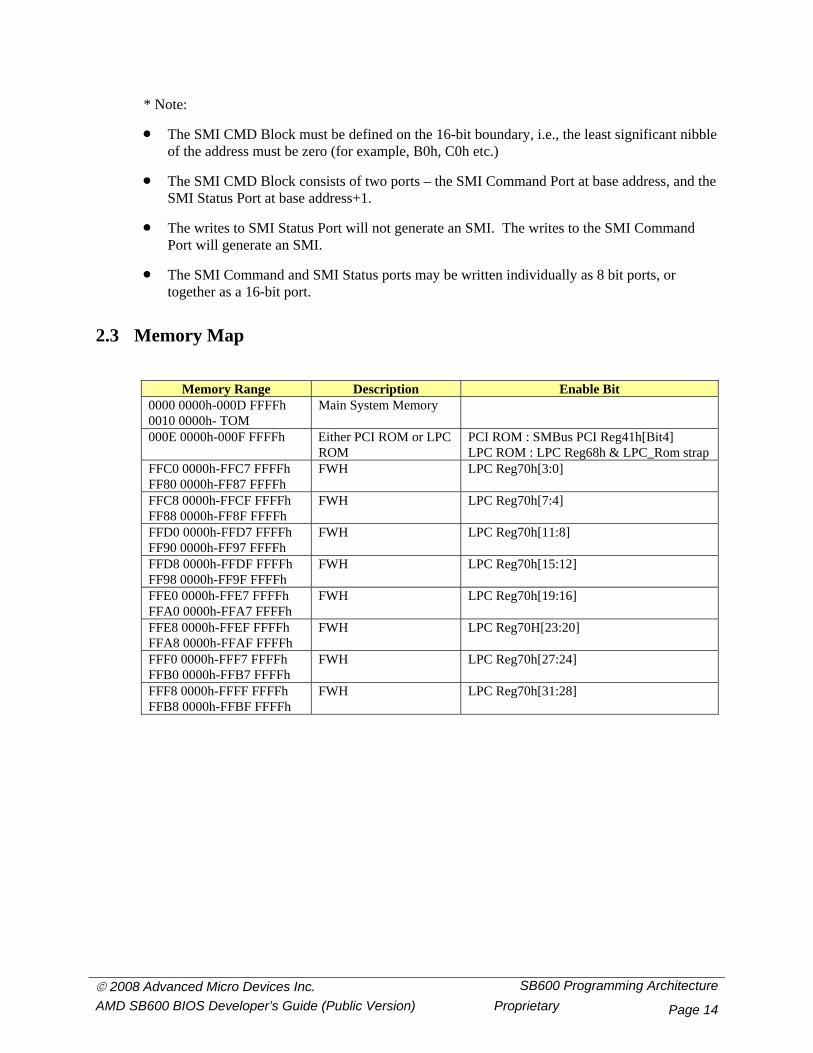
2.3 Memory Map
Memory Range Description Enable Bit
0000 0000h-000D FFFFh 0010 0000h- TOM
Main System Memory
000E 0000h-000F FFFFh Either PCI ROM or LPC ROM
PCI ROM : SMBus PCI Reg41h[Bit4] LPC ROM : LPC Reg68h & LPC_Rom strap
FFC0 0000h-FFC7 FFFFh FF80 0000h-FF87 FFFFh
FWH LPC Reg70h[3:0]
FFC8 0000h-FFCF FFFFh FF88 0000h-FF8F FFFFh
FWH LPC Reg70h[7:4]
FFD0 0000h-FFD7 FFFFh FF90 0000h-FF97 FFFFh
FWH LPC Reg70h[11:8]
FFD8 0000h-FFDF FFFFh FF98 0000h-FF9F FFFFh
FWH LPC Reg70h[15:12]
FFE0 0000h-FFE7 FFFFh FFA0 0000h-FFA7 FFFFh
FWH LPC Reg70h[19:16]
FFE8 0000h-FFEF FFFFh FFA8 0000h-FFAF FFFFh
FWH LPC Reg70H[23:20]
FFF0 0000h-FFF7 FFFFh FFB0 0000h-FFB7 FFFFh
FWH LPC Reg70h[27:24]
FFF8 0000h-FFFF FFFFh FFB8 0000h-FFBF FFFFh
FWH LPC Reg70h[31:28]

© 2008 Advanced Micro Devices Inc. SB600 Early-POST Initialization AMD SB600 BIOS Developer’s Guide (Public Version) Proprietary Page 15
3 SB600 Early-POST Initialization
The system BIOS needs to configure the SB600 at the very beginning of POST. Some of the settings will change depending on the OEM design, or on the newer revision chipset.
3.1 512K/1M ROM Enable
With the SB600 design, there can be two possible ROM sources: PCI ROM and LPC ROM. Two pin straps (UseLpcRom, FWHDisable) decide where the ROM is (see the SB600 databook). Upon system power on, the SB600 enables 256K ROM by default. The BIOS needs to enable 512K ROM or up to 1M for LPC ROM, if required.
3.1.1 PCI ROM
Control Bit Description 256K ROM (Default)
512K ROM Setting
SMBus PCI Reg41h[Bit1] When set to 1, the address between FFF80000h to FFFDFFFFh will be directed to the PCI ROM interface.
0 1
SMBus PCI Reg41h[Bit4] When set to 1, the address between 0E0000h to 0EFFFFh will be directed to the PCI ROM interface.
0 1
3.1.2 LPC ROM
To use the LPC ROM, the pin straps UseLpcRom, FWHDisable must be set accordingly.
Control Bit(s) Description Default 512K ROM Setting
1 M ROM Setting
LPC PCI Reg68h
16-bit starting & end address of the LPC ROM memory address range 1. 000E0000h 000E0000h 000E0000h
LPC PCI Reg6Ch 16-bit starting & end address of the LPC ROM memory address range 2.
FFFE0000h FFF80000h FFF00000h
LPC PCI Reg48Hh[Bits4:3]
Enable bits for LPC ROM memory address range 1 & 2. Note: with pins straps set to LPC ROM, these two bits have no effect on Reg68 & Reg6C.
00b 11b 11b
3.1.3 LPC ROM Read/Write Protect
The SB600 allows all or a portion of the LPC ROM addressed by the firmware hub to be read protected, write protected, or both read and write protected. Four dword registers are provided to select up to 4 LPC ROM ranges for read or write protection. The ROM protection range is defined by the base address and the length. The base address is aligned at a 2K boundary. The address length can be from 1K to 256K in increments of 1K.

© 2008 Advanced Micro Devices Inc. SB600 Early-POST Initialization AMD SB600 BIOS Developer’s Guide (Public Version) Proprietary Page 16
Register 50h, 54h, 58h, 5ch of Device 14h, Function 3
Field Name Bits Description Base Address 31:11 ROM Base address. The most significant 21 bits of the base address are
defined in this field. Bits 10:0 of the base address are assumed to be zero. Base address, therefore, is aligned at a 2K boundary.
Length 10:2 These 9 bits (0-511) define the length from 1K to 512K in increments of 1K.
Read Protect 1 When set, the memory range defined by this register is read protected. Reading any location in the range returns FFh.
Write Protect 0 When set, the memory range defined by this register is write protected. Writing to the range has no effect.
Example:
Protect 32K LPC ROM starting with base address FFF80000.
Base address bits 31:11 1111 1111 1111 1000 0000 0 b
Length 32K bit 10:2 = 31h = 000 0111 11 b
Read protect bit 1 = 1
Write protect bit 0 = 1
Register 50h = 1111 1111 1111 1000 0000 0000 0111 1111 b = FFF8007F h
Note:
1. Registers 50h ~ 5Fh can be written once after the hardware reset. Subsequent writes to them have no effect.
2. Setting sections of the LPC ROM to either read or write protect will not allow the ROM to be updated by a flash programming utility. Most flash utilities write and verify ROM sectors, and will terminate programming if verification fails due to read protect.
3.1.4 SPI ROM controller
The SPI ROM interface is a new feature added to the SB600. Refer to the AMD SB600 Register Reference Guide for more information on this feature. Note: The LPC ROM Read/Write Protect mentioned in the previous paragraph also applies to SPI. Two strap pins, PCICLK0 and PCICLK1, determine the SB600 boot up from LPC ROM or SPI ROM. There is no register status to reflect whether the current ROM interface is LPC or SPI.

© 2008 Advanced Micro Devices Inc. SB600 Early-POST Initialization AMD SB600 BIOS Developer’s Guide (Public Version) Proprietary Page 17
3.2 Real Time Clock (RTC)
3.2.1 RTC Access
The internal RTC is divided into two sections: the clock and alarm function (registers 0 to 0Dh), and CMOS memory (registers 0Eh to FFh). The clock and alarm functions must be accessed through I/O ports 70h/71h. The CMOS memory (registers 0Eh to FFh) should be accessed through I/O ports 72h/73h.
3.2.1.1 Special Locked Area in CMOS
Some CMOS memory locations may be disabled for read/write. Register 6Ah of SMBus (Bus 0, Device 14h, Function 0) has bits to disable these CMOS memory locations. These bits can be written only once after each power up reset or PCI reset.
RTCProtect- RW - 8 bits - [PCI_Reg: 6Ah]
Field Name Bits Default Description RTCProtect 0 0h When set, RTC RAM index 38h:3Fh will be locked from
read/write. This bit can only be written once. RTCProtect 1 0h When set, RTC RAM index F0h:FFh will be locked from
read/write. This bit can only be written once. RTCProtect 2 0h When set, RTC RAM index E0h:EFh will be locked from
read/write. This bit can only be written once. RTCProtect 3 0h When set, RTC RAM index D0h:DFh will be locked from
read/write. This bit can only be written once. RTCProtect 4 0h When set, RTC RAM index C0h:CFh will be locked from
read/write. This bit can only be written once. Reserved 7:5 0h
3.2.1.2 Century Byte
The RTC has a century byte at CMOS location 32h. Century is stored in a single byte and the BCD format is used for the century (for example, 20h for the year 20xx). This byte is accessed using I/O ports 70h and 71h. (The BIOS must set PMIO register 7Ch bit 4 to 1 to use this century byte at CMOS location 32h
3.2.1.3 Date Alarm
The RTC has a date alarm byte. This byte is accessed as follows:
1. Set to 1 the RTC register 0Ah , bit 4, using I/O ports 70h and 71h.
2. Write Date Alarm in BCD to register 0Dh using I/O ports 70h and 71h.
3. Clear to 0 the RTC register 0Ah bit 4 using I/O ports 70h and 71h.
Note: It is important to clear RTC register 0Ah bit 4 to zero; otherwise, the CMOS memory may not be accessed correctly from this point onward.

© 2008 Advanced Micro Devices Inc. SB600 Early-POST Initialization AMD SB600 BIOS Developer’s Guide (Public Version) Proprietary Page 18
3.3 BIOS RAM
The SB600 has 256 bytes of BIOS RAM. Data in this RAM is preserved until RSMRST# or S5 is asserted, or until power is lost.
This RAM is accessed using index and data registers at CD4h/CD5h.
3.4 Serial IRQ
The SB600 supports serial IRQ, which allows one single signal to report multiple interrupt requests. The SB600 supports a message for 21 serial interrupts, which include 15 IRQs, SMI#, IOCHK#, and 4 PCI interrupts.
SMBus PCI Reg69h is used for setting serial IRQ.
Bits in SMBus PCI Reg69 Description Power-on
Default Recommended Value
7 1 – Enables the serial IRQ function 0 – Disables the serial IRQ function
0 1
6 1 – Active (quiet) mode 0 – Continuous mode
0 0
5:2 Total number of serial IRQs = 17 + NumSerIrqBits 0 – 17 serial IRQs (15 IRQs, SMI#, IOCHK#) 1 – 18 serial IRQs (15 IRQs, SMI#, IOCHK#, INTA#) ... 15 - 32 serial IRQ's The SB600 serial IRQ can support 15 IRQs, SMI#, IOCHK#, INTA#, INTB#, INTC#, and INTD#.
0 0100b
1:0 Number of clocks in the start frame 0 00b Note: The BIOS should enter the continuous mode first when enabling the serial IRQ protocol, so that the SB600 can generate the start frame.
© 2008 Advanced Micro Devices Inc. SB600 Early-POST Initialization AMD SB600 BIOS Developer’s Guide (Public Version) Proprietary Page 19
3.5 SubSystemID and SubSystem Vendor ID
SubSytem ID and SubSystem Vendor ID can be programmed in various functions of SB600 register 2Ch. These registers are write-once registers. For example, to program a SubSystem vendor ID of 1002h and SubSystem ID of 4341h in AC97 device 14h, function 5, use the following assembly language sample code:
mov eax,8000A52Ch
mov dx,0CF8h
out dx,eax
mov dx,0CFCh
mov eax,43411002h
out dx,eax
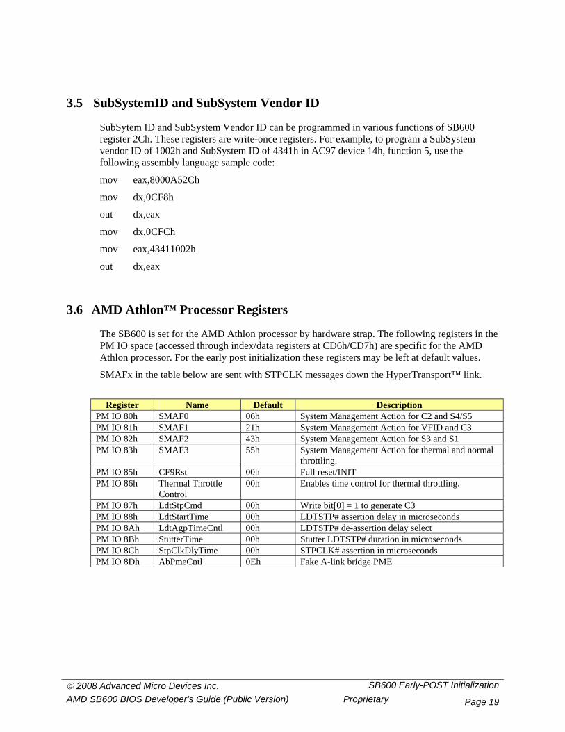
3.6 AMD Athlon™ Processor Registers
The SB600 is set for the AMD Athlon processor by hardware strap. The following registers in the PM IO space (accessed through index/data registers at CD6h/CD7h) are specific for the AMD Athlon processor. For the early post initialization these registers may be left at default values.
SMAFx in the table below are sent with STPCLK messages down the HyperTransport™ link.
Register Name Default Description
PM IO 80h SMAF0 06h System Management Action for C2 and S4/S5 PM IO 81h SMAF1 21h System Management Action for VFID and C3 PM IO 82h SMAF2 43h System Management Action for S3 and S1 PM IO 83h SMAF3 55h System Management Action for thermal and normal
throttling. PM IO 85h CF9Rst 00h Full reset/INIT PM IO 86h Thermal Throttle
Control 00h Enables time control for thermal throttling.
PM IO 87h LdtStpCmd 00h Write bit[0] = 1 to generate C3 PM IO 88h LdtStartTime 00h LDTSTP# assertion delay in microseconds PM IO 8Ah LdtAgpTimeCntl 00h LDTSTP# de-assertion delay select PM IO 8Bh StutterTime 00h Stutter LDTSTP# duration in microseconds PM IO 8Ch StpClkDlyTime 00h STPCLK# assertion in microseconds PM IO 8Dh AbPmeCntl 0Eh Fake A-link bridge PME

© 2008 Advanced Micro Devices Inc. SB600 Early-POST Initialization AMD SB600 BIOS Developer’s Guide (Public Version) Proprietary Page 20
3.7 System Restart after Power Fail
The way the system restarts following the power-fail/ power-restore cycle depends both on the PMIO register 74h [bits 1:0], and the hardware jumper on the SB600 pin ACPWR_Strap.
PMIO Register 74h bits[1:0]
Description
00b The system restart will depend on the ACPWR_Strap pin pull up/down state. Pin = 0 : The system will restart without pressing the power button Pin = 1 : The system will remain off until the power button in pressed.
01b The system will always restart after the power is restored. 10b The system will remain off until the power button is pressed. 11b At power-up the system will either restart or remain off depending on the state of the
system at power failure. If the system was on when the power failed, the system will restart at power-up. If the system was off when the power failed, the system will remain off after the power is restored. Pressing the power button is required to restart the system.
Notes on programming the PMIO register 74h:
1. PMIO register bits[3:0] should be used for programming. Bits[7:4] are read-only bits and reflect the same values as bits[3:0].
2. Bit2 is used by the hardware to save the power on/off status. This bit should not be modified during Software/BIOS programming. The BIOS programmer should always read the PMIO register 74h, modify bit3 and bits[1:0] as required, and write back the PMIO register 74h.
3.7.1 Power Fail and Alarm Setup
The state of the machine after the power-fail/power-restore cycle is controlled by PMIO register 74h bits[1:0] as described above. This programming can be over-ridden for the special case when the alarm is set. When both the alarm and the PMIO register 74h bit3 are set, the system will restart after the power is restored, regardless of how register 74h bits [1:0] are defined.

© 2008 Advanced Micro Devices Inc. PCI IRQ Routing AMD SB600 BIOS Developer’s Guide (Public Version) Proprietary Page 21
4 PCI IRQ Routing
4.1 PCI IRQ Routing Registers
The SB600 uses one pair of I/O ports to do the PCI IRQ routing. The ports are at C00h/C01h.
Address Register Name Description C00h PCI_Intr_Index PCI IRQ Routing Index
0 – INTA# 1 – INTB# 2 – INTC# 3 – INTD# 4 – SCI 5 – SMBus interrupt 9 – INTE# 0Ah – INTF# 0Bh – INTG# 0Ch – INTH#
C01h PCI_Intr_Data 0 ~ 15 : IRQ0 to IRQ15 IRQ0, 2, 8, 13 are reserved
4.2 PCI IRQ BIOS Programming
PCI IRQs are assigned to interrupt lines using I/O ports at C00h and C01h in index/data format. The register C00h is used for index as written with index number 0 through 0Ch as described in section 4.1 above. Register C01h is written with the interrupt number as data.
The following assembly language example assigns INTB# line to interrupt 10 (0Ah).
mov dx,0C00h ; To write to IO port C00h
mov al,02h ; Index for PCI IRQ INTB# as defined in section 4.1
out dx,al ; Index is now set for INTB#
mov dx,0C01h ; To write interrupt number 10 (0Ah)
mov al,0Ah ; Data is interrupt number 10 (0Ah )
out dx,al ; Assign IRQB# to interrupt 10
© 2008 Advanced Micro Devices Inc. PCI IRQ Routing AMD SB600 BIOS Developer’s Guide (Public Version) Proprietary Page 22
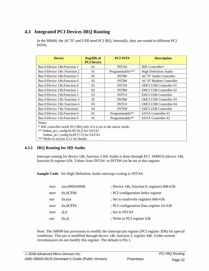
4.3 Integrated PCI Devices IRQ Routing
In the SB600, the AC’97 and USB need PCI IRQ. Internally, they are routed to different PCI INT#s.
Device Reg3Dh of PCI Device
PCI INT# Description
Bus 0:Device 14h:Function 1 01 INTA# IDE Controller* Bus 0:Device 14h: Function 2 01 Programmable*** High Definition Audio Bus 0:Device 14h:Function 5 02 INTB# AC’97 Audio Controller Bus 0:Device 14h:Function 6 02 INTB# AC’97 Modem Controller Bus 0:Device 13h:Function 0 01 INTA# OHCI USB Controller #1 Bus 0:Device 13h:Function 1 02 INTB# OHCI USB Controller #2 Bus 0:Device 13h:Function 2 03 INTC# EHCI USB Controller Bus 0:Device 13h: Function 3 02 INTB# OHCI USB Controller #3 Bus 0:Device 13h: Function 4 03 INTC# OHCI USB Controller #4 Bus 0:Device 13h: Function5 04 INTD# EHCI USB Controller Bus 0:Device 12h:Function 0 01 Programmable** SATA Controller #1 Bus 0:Device 11h:Function 0 01 Programmable** SATA Controller #2 Notes: * IDE controller needs PCI IRQ only if it is set to the native mode. ** Smbus_pci_config 0xAF [4:2] for SATA1 Smbus_pci_config 0xAF [7:5] for SATA2 *** Refer to section 4.3.1 for details.
4.3.1 IRQ Routing for HD Audio
Interrupt routing for device 14h, function 2 HD Audio is done through PCI SMBUS (device 14h, function 0) register 63h. Values from INTA# to INTH# can be set in this register.
Sample Code: Set High Definition Audio interrupt routing to INTA#:
mov eax,8000A060h ; Device 14h, function 0, registers 60h-63h
mov dx,0CF8h ; PCI configuration Index register
out dx,eax ; Set to read/write registers 60h-63h
mov dx,0CFFh ; PCI configuration Data register for 63h
mov al,0 ; Set to INTA#
out dx,al ; Write to PCI register 63h
Note: The SB600 has provisions to modify the interrupt pin register (PCI register 3Dh) for special conditions. This pin is modified through device 14h, function 2, register 44h. Under normal circumstances do not modify this register. The default is Pin 1.

© 2008 Advanced Micro Devices Inc. PCI IRQ Routing AMD SB600 BIOS Developer’s Guide (Public Version) Proprietary Page 23
4.4 PCI IRQ Routing for APIC Mode
PCI IRQ APIC Assignment INTA# 16 INTB# 17 INTC# 18 INTD# 19 INTE# 20 INTF# 21 INTG# 22 INTH# 23

© 2008 Advanced Micro Devices Inc. SMBus Programming AMD SB600 BIOS Developer’s Guide (Public Version) Proprietary Page 24
5 SMBus Programming
The SB600 SMBus (System Management Bus) complies with SMBus Specification Version 2.0.
5.1 SMBus I/O Base Address
The BIOS needs to set a valid SMBus I/O base address before enabling the SMBus Controller. There are two places at which the BIOS is able to set the SMBus I/O base addresses: one is at PCI Reg10h, another is at PCI Reg90h, and both are on the SMBus Controller (Bus 0, Device 14h, Function 0).
Before the BAR register, Reg10h, is assigned automatically during PCI bus enumeration, the BIOS needs to give a temporary SMBus I/O base address for accessing devices on the SMBus.
The SMBus controller enable bit is bit 0, register D2h, of the SMBus device (Bus 0, Device 14h, Function 0).
The following is a sample code to enable the SMBus with a temporary I/O base address:
SMB_IO EQU 8040h
; Set SMBus I/O base address
mov dx, 0CF8h ; PCI Index Register
mov eax, 8000A090h ; Reg90h on SMBus PCI Controller
out dx, eax
mov dx, 0CFCh ; PCI Data Register
mov eax, SMB_IO ; temp SMBus I/O base address
out dx, eax
; Enable the SMBus controller
mov dx, 0CF8h ; PCI Index Register
mov eax, 8000A0D0h ; RegD0 on SMBus PCI Controller
out dx, eax
mov dx, 0CFEh ; PCI Data Register
in al, dx ; read back from RegD2h
or al, 01 ; bit0 for enabling SMBus Controller interface
out dx, al
5.2 SMBus Timing
The SMBus frequency can be adjusted using different values in an 8-bit I/O register at the SMBus base + 0Eh location.
The SMBus frequency is set as follows:
SMBus Frequency = (Primary A-Link Clock )/(Count in index 0Eh * 4)

© 2008 Advanced Micro Devices Inc. SMBus Programming AMD SB600 BIOS Developer’s Guide (Public Version) Proprietary Page 25
The power-up default value in register 0Eh is A0h, therefore the default frequency is (66MHz)/(160 * 4), or approximately 103 KHz.
The minimum SMBus frequency can be set with the value FFh in the register at index 0Eh, which yields:
(66MHz)/(255*4) = 64.7 KHz.
5.3 SMBus Host Controller Programming
Step Descriptions Register in
SMBus I/O Space
Comments
1 Wait until SMBus is idle. Reg00h[Bit0] 0 – Idle 1 – Busy
2 Clear SMBus status. Reg00h[Bit4:1] Write all 1’s to clear 3 Set SMBus command. Reg03h The command will go to SMBus device. 4 Set SMBus device address with
read/write protocol Reg04h Bit7:1 – address
Bit0 – 1 for read, 0 for write 5 Select SMBus protocol Reg02h[Bit4:2] 6 Do a read from Reg02 to reset the
counter if it’s going to be a block read/write operation
Reg02h
7 Set low byte when write command Reg05h Byte command – It is the written data Word command – It is the low byte data Block command – It is block count Others – Don’t care
8 Set high byte when write command Reg06h Word command – It is the high byte data Others – Don’t care
9 Write the data when block write Reg07h Block write – write data one by one to it Others – Don’t care
10 Start SMBus command execution Reg02h[Bit6] Write 1 to start the command 11 Wait for host not busy Reg00h[Bit0] 12 Check status to see if there is any
error Reg00h[Bit4:2] With 1 in the bit, there is error
13 Read data Reg05h Byte command – It is the read data Word command – It is the low byte data Block command – It is block count Others – Don’t care
14 Read data Reg06h Word command – It is the high byte data Others – Don’t care
15 Read the data when block write Reg07h Block read – read data one by one. Others – Don’t care
The following flow chart illustrates the steps in programming the SMBus host controller.

© 2008 Advanced Micro Devices Inc. SMBus Programming AMD SB600 BIOS Developer’s Guide (Public Version) Proprietary Page 26
© 2008 Advanced Micro Devices Inc. IDE Controller AMD SB600 BIOS Developer’s Guide (Public Version) Proprietary Page 27
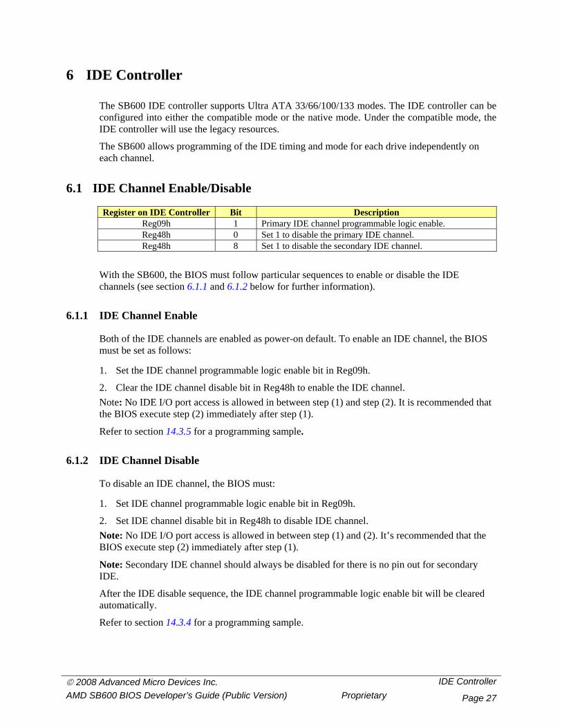
6 IDE Controller
The SB600 IDE controller supports Ultra ATA 33/66/100/133 modes. The IDE controller can be configured into either the compatible mode or the native mode. Under the compatible mode, the IDE controller will use the legacy resources.
The SB600 allows programming of the IDE timing and mode for each drive independently on each channel.
6.1 IDE Channel Enable/Disable
Register on IDE Controller Bit Description Reg09h 1 Primary IDE channel programmable logic enable. Reg48h 0 Set 1 to disable the primary IDE channel. Reg48h 8 Set 1 to disable the secondary IDE channel.
With the SB600, the BIOS must follow particular sequences to enable or disable the IDE channels (see section 6.1.1 and 6.1.2 below for further information).
6.1.1 IDE Channel Enable
Both of the IDE channels are enabled as power-on default. To enable an IDE channel, the BIOS must be set as follows:
1. Set the IDE channel programmable logic enable bit in Reg09h.
2. Clear the IDE channel disable bit in Reg48h to enable the IDE channel. Note: No IDE I/O port access is allowed in between step (1) and step (2). It is recommended that the BIOS execute step (2) immediately after step (1).
Refer to section 14.3.5 for a programming sample.
6.1.2 IDE Channel Disable
To disable an IDE channel, the BIOS must:
1. Set IDE channel programmable logic enable bit in Reg09h.
2. Set IDE channel disable bit in Reg48h to disable IDE channel. Note: No IDE I/O port access is allowed in between step (1) and (2). It’s recommended that the BIOS execute step (2) immediately after step (1).
Note: Secondary IDE channel should always be disabled for there is no pin out for secondary IDE.
After the IDE disable sequence, the IDE channel programmable logic enable bit will be cleared automatically.
Refer to section 14.3.4 for a programming sample.

© 2008 Advanced Micro Devices Inc. IDE Controller AMD SB600 BIOS Developer’s Guide (Public Version) Proprietary Page 28
6.2 PIO Modes
The SB600 supports IDE PIO mode 0, 1, 2, 3, and 4. For PIO mode selection, the BIOS needs to program not only the PIO mode register, but also the PIO timing register.
6.2.1 PIO Mode
The BIOS can simply give the PIO mode number through Reg4Ah on the IDE controller.
6.2.2 PIO Timing
Two parameters determine the PIO bus-cycle timing: the command width and the recovery width.
CT (bus-cycle timing) = 30ns * ((command width + 1) + (recovery width + 1))
For each PIO mode, the command width and the recovery width must be set by the BIOS accordingly:
PIO Mode Command Width (In Reg40h)
Recovery Width (In Reg40h) CT
0 9 9 600ns = 30 * ((9+1) + (9+1)) 1 4 7 390ns = 30 * ((4+1) + (7+1)) 2 3 4 270ns = 30 * ((3+1) + (4+1)) 3 2 2 180ns = 30 * ((2+1) + (2+1)) 4 2 0 120ns = 30 * ((2+1) + (0+1))
6.3 DMA Modes
The SB600 IDE controller can run at either the legacy (Multi-Words) DMA mode, or the Ultra-DMA mode.
6.3.1 Legacy (Multi-Words) DMA mode
The SB600 IDE controller will run at the legacy DMA mode only when the Ultra-DMA mode is disabled.
Two parameters determine the DMA bus-cycle timing: the command width and the recovery width.
CT (bus-cycle timing) = 30ns * ((command width + 1) + (recovery width + 1))
For each legacy DMA mode, the command width and recovery width must be set by the BIOS accordingly:
Legacy DMA Mode
Command Width (In Reg44h)
Recovery Width (In Reg44h) CT
0 7 7 480ns = 30 * ((7+1) + (7+1)) 1 2 1 150ns = 30 * ((2+1) + (1+1)) 2 2 0 120ns = 30 * ((2+1) + (0+1))

© 2008 Advanced Micro Devices Inc. IDE Controller AMD SB600 BIOS Developer’s Guide (Public Version) Proprietary Page 29
6.3.2 Ultra-DMA Mode
The SB600 IDE controller supports UDMA mode 0, 1, 2, 3, 4, 5, and 6.
It only takes two simple steps to program the SB600 IDE controller into the UDMA mode:
1. Set the mode number in UDMA mode register (Reg56h).
2. Enable the UDMA mode through the UDMA control register (Reg54h). The UDMA bus-cycle timing is fixed after the UDMA mode is selected.
UDMA Mode Bus-Cycle Timing (ns) 0 120 1 90 2 60 3 45 4 30 5 20 6 15

© 2008 Advanced Micro Devices Inc. Serial ATA (SATA) AMD SB600 BIOS Developer’s Guide (Public Version) Proprietary Page 30
7 Serial ATA (SATA)
The SB600 has two SATA devices. For ASIC revision A21, they are at Bus 0, Device 12h, Function 0 and Bus 0, Device 11h, Function 0. For revisions A11 and A12, they are at Bus 0, Device 13h, Function 3 and Function 4. The SATA devices are enabled/disabled through a register at ADh in the SMBus controller (Device 14h, function 0).
MiscSata - RW - 8 bits - [PCI_Reg: ADh]
Field Name Bits Default Description
SATA Enable 0 1 SATA enable SataSmbusEn 1 0 SATA SMBus enable SataSmbusMode 2 0 SATA SMBus mode, set to 1 to put SATA I2C on GPIO pins SataPsvEn Enable
5 1 SATA power saving enable
MiscSata register
The SATA option ROM initial load size is 64KB, and the run time size is 2KB.
A SATA controller enable/disable sample code is found in section 14.2.5.
A SATA class ID change sample code is found in section 14.2.6.
7.1 SATA Hot Plug
The SATA hot plug feature is implemented through the following registers:
1. ACPI GPE0 Block status register bit 31 for SCI status.
2. ACPI GPE0 Block enable register bit 31 for SCI enable.
3. PMIO register 37h bit 2 to trigger SATA hot plug SCI.
1 = Rising edge.
0 = Falling edge trigger.
4. The SATA internal status is set whenever a SATA hard drive is plugged in, unplugged, powered up, or powered down. The status registers are:
Register BAR 5 + 10Ah, bit 0, for primary channel.
Register BAR 5 + 18Ah, bit 0, for secondary channel.
7.1.1 Sample Code
See section 14.7 for the SATA Hot Plug sample code.

© 2008 Advanced Micro Devices Inc. Power Management AMD SB600 BIOS Developer’s Guide (Public Version) Proprietary Page 31
8 Power Management
On the SB600, PM registers can be accessed through I/O ports CD6h/CD7h. Before initiating any power management functions in the SB600, the BIOS needs to set the I/O base addresses for the ACPI I/O register, the SMI Command Port, etc.
I/O Name Description Configure Register Range Size (Bytes)
PM1_EVT ACPI PM1a_EVT_BLK PM IO Reg20h & Reg21h 4 PM1_CNT ACPI PM1a_CNT_BLK PM IO Reg22h & Reg23h 2 PM_TMR ACPI PM_TMR_BLK PM IO Reg24h & Reg25h 4 P_BLK ACPI P_BLK PM IO Reg26h & Reg27h 6 GPE0_EVT ACPI GPE0_EVT_BLK PM IO Reg28h & Reg29h 8 SMI CMD Block * SMI Command Block PM IO Reg2Ah & Reg2Bh 2
* Notes:
• The SMI CMD Block must be dword aligned, i.e., the least significant two bits of the address must be zero (address[1:0] must be 00). For example, B0h, B4h, B8h, BCh, etc.
• The SMI CMD Block consists of two ports – the SMI Command Port at base address, and the SMI Status Port at base address+1.
• The writes to the SMI Status Port will not generate an SMI. The writes to the SMI Command Port will generate an SMI.
• The SMI Command and SMI Status ports may be written individually as 8 bit ports, or together as a 16 bit port.
8.1 SMI Handling – EOS (PM IO Reg10h[Bit0])
Upon each SMI generation, the SB600 will clear the EOS bit automatically. At the end of the SMI service, the BIOS needs to clear the status bit of the SMI event and re-enable the EOS; otherwise, the SB600 will not be able to generate SMI, even if SMI events arrive.
8.2 Programmable I/Os
There are eight sets of programmable I/Os available on the SB600. The BIOS can use them for I/O trapping, which means that an SMI will be generated if any access falls into the PIO range.
The PIO address range can be set to 2, 4, 8, and 16.
I/O Name Description Configure Register Enable Status PIO0 Programmable I/O Range 0 PM IO Reg14h & Reg15h PM IO Reg1Ch[Bit7] PM IO Reg1Dh[Bit7]PIO1 Programmable I/O Range 1 PM IO Reg16h & Reg17h PM IO Reg1Ch[Bit6] PM IO Reg1Dh[Bit6]PIO2 Programmable I/O Range 2 PM IO Reg18h & Reg19h PM IO Reg1Ch[Bit5] PM IO Reg1Dh[Bit5]PIO3 Programmable I/O Range 3 PM IO Reg1Ah & Reg1Bh PM IO Reg1Ch[Bit4] PM IO Reg1Dh[Bit4]

© 2008 Advanced Micro Devices Inc. Power Management AMD SB600 BIOS Developer’s Guide (Public Version) Proprietary Page 32
I/O Name Description Configure Register Enable Status PIO4 Programmable I/O Range 4 PM IO RegA0 & RegA1h PM IO Reg A8h[Bit0] PM IO RegA9h[Bit0]PIO5 Programmable I/O Range 5 PM IO RegA2 & RegA3h PM IO Reg A8h[Bit1] PM IO RegA9h[Bit1]PIO6 Programmable I/O Range 6 PM IO RegA4 & RegA5h PM IO Reg A8h[Bit2] PM IO RegA9h[Bit2]PIO7 Programmable I/O Range 7 PM IO RegA6 & RegA7h PM IO Reg A8h[Bit3] PM IO RegA9h[Bit3]
Note: PM IO Reg04h[Bit7] is the overall control bit for enabling all the PIOs. The BIOS must set it before using any PIO.
8.3 Power Management Timers
There are two PM timers available on the SB600 – PM Timer 1 and PM Timer 2. The PM Timer 1 (Inactivity Timer) can be programmed to reload on some activities, but not the PM Timer 2 (Activity Timer).
8.3.1 PM Timer 1 (Inactivity Timer)
The PM Timer 1 is a 6-bit timer with a granularity of 1 minute. The BIOS can set the initial value of the PM Timer 1 through PM IO Reg0Bh. PM IO Reg0Ch will return the current value of the decrementing counter.
The PM Timer 1 is typically used as a stand-by timer under the APM mode.
PM Timer1 Reloading On Description Enable IRQ[15:8] IRQ[15:8] activity. PM IO Reg08h[Bit7:0] IRQ[7:3], NMI, and IRQ[1:0] IRQ[7:3], NMI, and IRQ[1:0] activity PM IO Reg09h[Bit7:0] Programmable IO Any access to PIO ports. PM IO Reg0Ah[Bit7] Parallel Port Parallel ports activity PM IO Reg0Ah[Bit6] Serial Port Serial Ports activity PM IO Reg0Ah[Bit5] IDE Port IDE port activity PM IO Reg0Ah[Bit4] Floppy Port Floppy port activity PM IO Reg0Ah[Bit3] Game Port Game port (201H) activity PM IO Reg0Ah[Bit2] ExtEvent1 Assert ExtEvent1 pin PM IO Reg0Ah[Bit1] ExtEvent0 Assert ExtEvent0 pin PM IO Reg0Ah[Bit0]
8.3.2 PM Timer 2 (Activity Timer)
The PM Timer 2 is an 8-bit timer with a granularity of 500 µs. The BIOS can set the initial value of the PM Timer 2 through PM IO Reg12h. PM IO Reg13h will return the current value of the decrementing counter.
Note: The PM Timer 2 cannot be configured to reload on any system activities.
8.4 SMI Events
The following is a list of all the SMI events available on the SB600. The events can only generate SMI, not SCI or wakeup events.
The global SMI disable bit is PM IO register 53h, bit [3].

© 2008 Advanced Micro Devices Inc. Power Management AMD SB600 BIOS Developer’s Guide (Public Version) Proprietary Page 33
PM IO register 53h bit [3] = 0 SMI# enabled (default)
PM IO register 53h bit [3] = 1 SMI# disabled (all events disabled)
SMI Source Description Enable Status Software SMI (obsolete way)
Set SmiReq (PM IO Reg00h[Bit4]) to generate SMI.
Always PM IO Reg01h[Bit4]
Software SMI Any writing to SMI Command port.
PM IO Reg0Eh[Bit2] PM IO Reg0Fh[Bit2]
PM Timer 1 Timeout on PM Timer 1. Activity on PM IO register 08h, 09h, 0Ah will retrigger timer
PM IO Reg00h[Bit1] PM IO Reg01h[Bit1]
PM Timer 2 Timeout on PM Timer 2. (See section 9.3.2)
PM IO Reg00h[Bit2] PM IO Reg01h[Bit2]
IRQ[15:8] IRQ[15:8] activity. PM IO Reg02h[Bit7:0] PM IO Reg05h[Bit7:0] IRQ[7:3], NMI, and IRQ[1:0]
IRQ[7:3], NMI, and IRQ[1:0] activity
PM IO Reg03h[Bit7:0] PM IO Reg06h[Bit7:0]
Programmable I/O Any access to PIO ports PM IO Reg04h[Bit7] AND
PM IO Reg1Ch[Bit7:4]
PM IO Reg1Dh[Bit7:4]
Parallel Port Parallel ports activity PM IO Reg04h[Bit6] PM IO Reg07h[Bit6] Serial Port Serial Ports activity PM IO Reg04h[Bit5] PM IO Reg07h[Bit5] IDE Port IDE port activity PM IO Reg04h[Bit4] PM IO Reg07h[Bit4] Floppy Port Floppy port activity PM IO Reg04h[Bit3] PM IO Reg07h[Bit3] Game Port Game port (201h) activity PM IO Reg04h[Bit2] PM IO Reg07h[Bit2] ExtEvent1 Assert ExtEvent1 pin PM IO Reg04h[Bit1] PM IO Reg07h[Bit1] ExtEvent0 Assert ExtEvent0 pin PM IO Reg04h[Bit0] PM IO Reg07h[Bit0] Mouse/Keyboard Mouse/Keyboard port activity PM IO Reg1Ch[Bit3] PM IO Reg1Dh[Bit3] Audio/MSS Audio/MSS port activity PM IO Reg1Ch[Bit2] PM IO Reg1Dh[Bit2] MIDI MINI port activity PM IO Reg1Ch[Bit1] PM IO Reg1Dh[Bit1] AD_LIB AD_LIB port activity PM IO Reg1Ch[Bit0] PM IO Reg1Dh[Bit0] SERR# port System error to report parity
errors or special cycle command or other catastrophic system errors.
PCI SMBus Reg 66h, bit[0]
PCI SMBus reg 04h, bit [30]. PM IO reg 0Fh[Bit 1]
Global Release Write
OS write to PM1 Control register
PM IO 0Eh[Bit 0] PM IO 0Fh[Bit0]
Temperature Warning
C50/C51, index 03, [bit1]
C50/C51, index 02, [bit1]

© 2008 Advanced Micro Devices Inc. Power Management AMD SB600 BIOS Developer’s Guide (Public Version) Proprietary Page 34
8.4.1 Power Button
Power button is always a wake-up event and can be programmed as an SCI wake-up event. The power button status register is AcpiPmEvtBlk, bit[8]. The BIOS must make sure this bit is cleared prior to the entry into any C or S states.
In addition, when the power button is pressed for 4 seconds, the SB600 will shut down the entire system (by going to S5). No programming is required for this function.
8.5 C-State Break Events
8.5.1 Break Events for C2 State
Under C2 the break events are as follows:
• PBE#
• Special_message from CPU (AMD Athlon™ mode)
• I/O write to special register (AMD Athlon mode)
• SMI#
• NMI
• INIT
• Interrupts (in PIC mode only)
8.5.2 Break Events for C3 and C4 States
All of the events listed (above) as break events in C2 state are also break events in C3 and C4 states. In addition, the Bus Master Status is also a break event in C3 and C4 states.
8.6 Save/Restore Sequence for S3 State
8.6.1 Register Save Sequence for S3 State
Prior to initiating S3 states, the BIOS must save the registers on the machine. The BIOS reserves a section of the memory and a section of the CMOS to save the registers. Depending on the BIOS architecture, these registers may be saved either one time just prior to handing of the control over to the OS, or every time just before going into the S3 states.
The following registers must be saved:
• Some Northbridge registers in CMOS
• Some Northbridge and Memory Controller registers
• Southbridge PCI registers on the SB600
• Southbridge non-PCI registers

© 2008 Advanced Micro Devices Inc. Power Management AMD SB600 BIOS Developer’s Guide (Public Version) Proprietary Page 35
• PCI registers not on the SB600
• Super I/O and other I/O registers.
The BIOS typically sets aside an area in the memory to save the registers prior to the S3 state. The Southbridge registers may be saved in any order as long as those registers are visible to the BIOS.
Some of the registers, such as SubSystem ID and SubSystem Vendor ID, may be saved, but written only once as dword. They are handled separately during restore.
8.7 Wake on Events
TBD
8.8 Sleep SMI Events
These events provide an SMI# before the system transits to an SX state (e.g. ACPI S1, S2, S3, S4, and S5). This feature helps the System BIOS to develop software workarounds or debugging routines before the system goes to sleep state.
8.8.1 Sleep SMI Control Register
There is a Sleep SMI control register in the SB600. Its base I/O address is defined at PMIO Reg 0x04.
SLP_SMI_EN is a R/W register bit for controlling a Sleep SMI when the system transits to an ACPI SX state. The register definition is as follows:
• SLP_SMI_EN [Bit7] = 0, Disables Sleep SMI event.
• SLP_SMI_EN [Bit7] = 1, Enables Sleep SMI event. There is a Sleep SMI Status register in the SB600. Its base I/O address is defined at PMIO Reg 0x07.
SLP_SMI_Status [Bit7] is asserted when the system goes to an ACPI SX state, and when SLP_SMI_EN is set to enable.
8.8.2 Sleep SMI Programming Sequence
8.8.2.1 Set Sleep SMI Control Register
The Sleep SMI Control Register does not necessary have to be enabled before the system goes to the ACPI SX state. One may enable the control the bit in the ACPI ASL code. Please refer to section 14.9 “Sleep Trap Through SMI#” for the sample code.
8.8.2.2 Enter Sleep SMI# Routine
The system does not go into the sleep state (set by ACPI PM1_CNT) when SMI# is asserted. The

© 2008 Advanced Micro Devices Inc. Power Management AMD SB600 BIOS Developer’s Guide (Public Version) Proprietary Page 36
System BIOS has to follow the sequence below:
1. Disable Sleep SMI Control register (SLP_SMI_EN). 2. Software workaround or system BIOS debugging routing implementation. 3. Write SLP_SMI_Status 1 to clear this event. 4. Rewrite sleep command to ACPI register (ACPI PM1_CNT). 5. RSM if necessary.

© 2008 Advanced Micro Devices Inc. APIC Programming AMD SB600 BIOS Developer’s Guide (Public Version) Proprietary Page 37
9 APIC Programming
With the AMD integrated chipset solution, the BIOS needs to program both the Northbridge and the Southbridge in order to support APIC.
9.1 Northbridge APIC Enable
There are three bits in the Northbridge that the BIOS should set before enabling APIC support.
• Enable Local APIC in AMD Athlon processors. (Set bit11 in APIC_BASE MSR(001B) register.)
• Reg4C[bit1] - This bit should be set to enable. It forces the CPU request with address 0xFECx_xxxx to the Southbridge.
• Reg4C[bit18] - This bit should be set to enable. It sets the Northbridge to accept MSI with address 0xFEEx_xxxx from the Southbridge.
9.2 Southbridge APIC Enable
There are two bits in the Southbridge that the BIOS should set before enabling APIC support.
• Reg64[bit3] = 1 to enable the APIC function. • Reg64[bit7] = 1 to enable the xAPIC function. It is only valid if Bit3 is being set.
9.3 IOAPIC Base Address
The IOAPIC base address can be defined at SMBus PCI Reg. 74h. The power-on default value is FEC00000h.
Note: This register is 32-bit access only. The BIOS should not use the byte restore mechanism to restore its value during S3 resume.
9.4 APIC IRQ Assignment
SB600 has IRQ assignments under APIC mode as follows:
• IRQ0~15 – legacy IRQ • IRQ 16 – PCI INTA • IRQ 17 – PCI INTB • IRQ 18 – PCI INTC • IRQ 19 – PCI INTD • IRQ 20 – PCI INTE • IRQ 21 – PCI INTF • IRQ 22 – PCI INTG • INT 23 – PCI INTH • IRQ 09 – ACPI SCI
SCI is still as low-level trigger with APIC enabled.

© 2008 Advanced Micro Devices Inc. APIC Programming AMD SB600 BIOS Developer’s Guide (Public Version) Proprietary Page 38
9.5 APIC IRQ Routing
During the BIOS POST, the BIOS will do normal PCI IRQ routing through port C00h/C01h. Once APIC is fully enabled by the OS, the routing in C00h/C01 must be all cleared to zero.
The following is a sample ASL code that may be incorporated into the BIOS:
Name(PICF,0x00) Method(_PIC, 0x01, NotSerialized) { Store (Arg0, PICF) If(Arg0) { \_SB.PCI0.LPC0.DSPI() // clear interrupt at 0xC00/0xC01 } } OperationRegion(PIRQ, SystemIO, 0xC00, 0x2) Field(PIRQ, ByteAcc, NoLock, Preserve) {
PIID, 8, PIDA, 8 } IndexField(PIID, PIDA, ByteAcc, NoLock, Preserve) {
PIRA, 8, PIRB, 8, PIRC, 8, PIRD, 8, PIRS, 8 Offset(0x09), PIRE, 8, PIRF, 8, PIRG, 8, PIRH, 8
} Method(DSPI) {
Store(0x00, PIRA) Store(0x00, PIRB) Store(0x00, PIRC) Store(0x00, PIRD) Store(0x00, PIRS) Store(0x00, PIRE) Store(0x00, PIRF) Store(0x00, PIRG) Store(0x00, PIRH)
}

© 2008 Advanced Micro Devices Inc. Watchdog Timer AMD SB600 BIOS Developer’s Guide (Public Version) Proprietary Page 39
10 Watchdog Timer
To enable the watchdog timer in the SB600, the following registers must be initialized:
• Enable the watchdog timer by resetting bit 0 in PMIO register 069h. • Set bit 3 in SMBus PCI Config (Bus 0 Device 20 Function 0) Reg 41h to enable the
watchdog decode. • Ensure that the watchdog timer base address is set to a non zero value, typically
0FEC000F0h. The watchdog base address is set at PMIO address 6Ch-6Fh as shown in the sample program below. (PMIO is addressed as byte index/data):
Sample Program:
mov dx,0CD6h ; PMIO index register
mov al,6Fh ; Most significant base address location
out dx,al ; Set the index to 6Fh
mov dx,0CD7h ; PMIO data register
mov al,0FEh ; Most significant base address
out dx,al
mov dx,0CD6h ; PMIO index register
mov al,6Eh ; Second significant base address location
out dx,al ; Set the index to 6Eh
mov dx,0CD7h ; PMIO data register
mov al,0C0h ; Second significant base address
out dx,al
mov dx,0CD6h ; PMIO index register
mov al,6Dh ; Third significant base address location
out dx,al ; Set the index to 6Dh
mov dx,0CD7h ; PMIO data register
mov al,00h ; Third significant base address
out dx,al

© 2008 Advanced Micro Devices Inc. Watchdog Timer AMD SB600 BIOS Developer’s Guide (Public Version) Proprietary Page 40
mov dx,0CD6h ; PMIO index register
mov al,6Ch ; Least significant base address location
out dx,al ; Set the index to 6Ch
mov dx,0CD7h ; PMIO data register
mov al,0F0h ; Least significant base address
out dx,al
To verify that the watchdog timer works correctly, perform the following steps:
• Write 100 (count) to the watchdog count register at address 0FEC000F4h. • Enable and start the watchdog timer by writing 00000081h to the watchdog control register at
0FEC000F0h. • The counter will start decrementing and will reset the system once it reaches 0. This means
that the watchdog timer is working as designed.

© 2008 Advanced Micro Devices Inc. A-Link Bridge AMD SB600 BIOS Developer’s Guide (Public Version) Proprietary Page 41
11 A-Link Bridge
11.1 A-Link Registers
The registers are accessed using an address-register/data-register mechanism. The address register is AB_INDX[31:0], and the data register is AB_DATA[31:0].
31:30 29:17 16:2 1:0
RegSpace[1:0] Reserved Register address[16:2] Reserved
AB_INDX [31:0]
31:0 Data[31:0]
AB_DATA[31:0]
RegSpace[1:0] 00b AXINDC Index/Data Registers. (AX_INDXC) 01b AXINPD Index/Data Registers (AX_INDXP) 10b A-Link Express Configuration (AXCFG) 11b A-Link Bridge Configuration (ABCFG)
Definition of RegSpace[1:0]
In order to read or write a particular register, the software will write the register address and the register space identifier to AB_INDX and then do a read or write to AB_DATA. This is analogous to how PCI configuration reads and writes work through I/O addresses CF8h/CFCh.
The location of AB_INDX in the I/O space is defined by the abRegBaseAddr register located at Device 14h, function 0, register 0F0h. The AB_DATA register address is offset 4h from the AB_INDX address. The address of the AB_INDX must be 8 byte aligned.
31:3 2:0 BaseAddr[31:3] Rsv
abRegBAR[31:0] at Bus 0, Device 14h, Function 0, Register 0F0h
AXCFG and ABCFG registers are accessed indirectly through AB_INDX/AB_DATA. To read or write a particular register through AB_INDX/AB_DATA, the register address and the register space identifier is first written to AB_INDX. The specified register is then accessed by doing a read or write to AB_DATA (see the example below).
Access to AXINDC and AXINDP registers requires a second level of indirection. Registers in these spaces are addressed through the following indirection registers: AX_INDEXC/AX_DATAC and AX_INDEXP/AX_DATAP.

© 2008 Advanced Micro Devices Inc. A-Link Bridge AMD SB600 BIOS Developer’s Guide (Public Version) Proprietary Page 42
Register Indirect Address
AX_INDXC 30h
AX_DATAC 34h
AX_INDXP 38h
AX_DATAP 3Ch
Example: To write to register 21h in the INDXC space with a data of 00, the following steps are required:
1. Out 30h to AB_INDX. This will prepare to write register from INDXC
2. Out 21h to AB_DATA. This will set register 21h of INDXC
3. Out 34h to AB_INDX. This will prepare to write data to register defined in steps 1 and 2 above
4. Out 00 to AB_DATA. This will write the data to the register defined n steps 1 and 2 above.
11.2 Programming Procedure
Indirect access is required to access both A-Link Express Configuration and A-Link Bridge Configuration register space. The programming procedure is as follows:
Write:
1. Set the A-Link bridge register access address. This address is set at device 14h, function 0, register 0F0h. This is an I/O address and needs to be set only once after power-up. The I/O address must be on a 8-byte boundary (i.e., 3 LS bits must be zeroes).
Example: To set C80h as an A-Link bridge register access address:
mov dx,0CF8h ; To access device 14h, function 0
mov eax,8000A0F0h ;
out dx,eax
mov dx,0CFCh
mov eax,00000C80h ; A-Link bridge register access address
out dx,eax
Note: Although the 32-bit I/O address is set for the A-Link bridge (e.g., 00000C80h), the bridge may be accessed by a 16-bit address (i.e., 0C80h). The MS word is set to 00 by default (see the example below).
2. Write the register address in the AB_INDX.
Example: To write to the A-Link Bridge configuration register space at 90h:
mov dx,0c80h ; I/O address index assigned to A-Link

© 2008 Advanced Micro Devices Inc. A-Link Bridge AMD SB600 BIOS Developer’s Guide (Public Version) Proprietary Page 43
mov eax, 0C0000090h ; Bits[31:30] = 11 for A-Link Bridge register ; space
out dx,eax ; Register index is set
mov dx,0c84h ; I/O address for data
mov eax,00000001h ; Power down 2 lanes to save power
out dx,eax
Read:
Use a similar indirect procedure to read out the register value inside AB and BIF.

© 2008 Advanced Micro Devices Inc. High Precision Event Timer (HPET) AMD SB600 BIOS Developer’s Guide (Public Version) Proprietary Page 44
12 High Precision Event Timer (HPET)
The SB600 includes an industry standard High Precision Event Timers (HPET). The details and the operation of the timer are described in the IA-PC HPET specification. This section describes the timer initialization in the SB600 chipset.
12.1 Initialization
For SB600 is HPET usage is required, then during the early POST, the timer base address must be programmed in Device 14h, Function 0, register 14h. This base address is also reported to the operating system through the ACPI table as specified in the specification. In addition, the HPET interrupts may also be enabled through Device 14h, Function 0, register 64h, bit 10.
12.1.1 Sample Initialization Code
HpetBaseAddress EQU 0FED00000H ; OEM specific address ; Set Base address in Device 14h, Function 0, Register 14h mov dx,0CF8h ; PCI index register mov eax,8000A014h ; Bus 0, Device 14h, Function 0, Register 14h out dx,eax ; Set PCI index to register 14h mov dx,0CFCh ; PCI data register mov eax,0FED00000h ; Base address, OEM specific out dx,eax ; Enable the HPET interrupts, if needed. Set Device 14h, Function 0, Register 64h, bit 10 mov dx,0CF8h ; PCI index register mov eax,8000A064h ; Bus 0, Device 14h, Function 0, Register 64h out dx,eax ; Set PCI index to register 64h mov dx,0CFCh ; PCI data register in eax,dx ; Read current value of register 64h or eax,00000400h ; Set bit 10 out dx,eax

© 2008 Advanced Micro Devices Inc. High Precision Event Timer (HPET) AMD SB600 BIOS Developer’s Guide (Public Version) Proprietary Page 45
12.2 ACPI HPET Description Table
As described in the specification, an ACPI HPET table is required to report the base address to the operating system. The table includes a ACPI table header, and HPET table-specific fields. The sample values for the HPET specific fields are as follows: Event Timer Block ID DD 00000000h ; Base Address (Lower 4 bytes) DD 00000800h ; Base Address (Middle 4 bytes) DD 0FED00000h ; Address on 32 bit system Base Address (Upper 4 bytes) DD 00000000h ; Used on 64 bit system HPET Number DB 00h ; Minimum Clock Tick DW 37EEh ; 14318 (decimal)
12.3 HPET Support for Longhorn
For the SB600, PM_IO register 72h bits [2:0] should be set to 111b for Longhorn support.

© 2008 Advanced Micro Devices Inc. Common Interface Module – CIM-SB600 AMD SB600 BIOS Developer’s Guide (Public Version) Proprietary Page 46
13 Common Interface Module – CIM-SB600
13.1 CIM-SB600 Architecture
CIM-SB600 employs a modular component design with an open interface definition such that the amount of functional components included, the sequence these components are called, and the way these components are called could all be different, depend on different requirements of different OEM projects/platforms.
CIM-SB600 requires bios code base provides addresses (for ex. SMBUS Base Address).
SB600-CIM can be divided into four functional sub modules:
• Power On Reset initialization (SBPOR)
• POST initialization.
• RUNTIME initialization.
• SMM Module
The following diagram is a conceptual overview of the AMD SB600-CIM infrastructure and its functional modules in relative with a typical system BIOS power on boot up timeframe. Each modular component (functional module) will be introduced in more detail in later chapters.

© 2008 Advanced Micro Devices Inc. Common Interface Module – CIM-SB600 AMD SB600 BIOS Developer’s Guide (Public Version) Proprietary Page 47
SBCIM - SBPOR Initialization Module
System PowerOn
Is S3 resume?Restore memory controller configuration
etcYes
SBCIM Runtime submodule -
AtiSbBfPciRestore
SBCIM Runtime sub module –1. Route SATA controllers to different AB-ports
depending on input parameters2. Program prefetch for IDE, USB and PCIB.3. Program SATA class code4. Restore Subsystem IDs for all the SB devices
Memory detection.System BIOS shadowingNO
SBCIM Post Initialization submodule – AtiSbBeforePciInit1. Reads the PCIE base address from NorthBridge and saves it for further use to do PCI config using MMIO access.2. Enable or Disable South Bridge devices depending on input data structure values.3. Reset usb controllers.4. Enable or disable thermal trip function.5. Call SBCIM Runtime submodules
PCI enumeration and resource allocation
Restore PCI devices and do other S3 resume
tasks
SBCIM Runtime submodule -
AtiSbAfPciRestore
SBCIM Runtime sub module –1.Initialize SATA PHY SBCIM Post Initialization
submodule –AtiSbAfterPciInit
1. Configure High definition Audio (Azalia)2.Detect and configure AC-97 modem3.Detect and configure MC-97 modem4.Initialize USB PHY settings and most of the other settings which are recommended in RPR.Do other S3 resume
tasks.Jump to Wakeup vector.
Configures all IO Devices.Enumerate USB Detect and Initialize boot devices Option ROM initliazationBIOS Setup etc
SBCIM Post Initialization submodule –
AtiSbLatePost 1.Initialize some of the PCI bridge registers which are recommended in RPR.2.Initialize the SBCIM SMI data structure 3.Program some of RPR settings for SATA controller
Load bootloader and give control to
OS
System BIOS SMI handler
Operating System
SBCIM SMI sub moduleAtiSbSmiService
1. Check & service if SMI due to keyboard reset
CPU Initialization, NorthBridge Initialization

© 2008 Advanced Micro Devices Inc. Common Interface Module – CIM-SB600 AMD SB600 BIOS Developer’s Guide (Public Version) Proprietary Page 48
13.2 CIM-SB600 Build Configuration
SBCIM module provides the BIOS developer the flexibility to assign their own values (for programmable options such as SMBUS port address). SB module configuration requirement from BIOS code base: Override Symbol Description ATI_BIOS_SIZE BIOS FlashROM size.
Set to 100000h if you are using 1MB flash part.
ATI_SMBUS_BASE_ADDRESS
SMBus base address(I2C port address); by default , ASF Base Address is set ATI_SMBUS _BASE_ADDRESS +10h
ATI_SIO_PME_BASE_ADDRESS This is a base for SIO PME
sb_acpi_base_tbl: acpi_base STRUC pm1evt dw ? ;pmio 2ah pm1ctr dw ? pmtmr dw ? cpuctr dw ? gpe0 dw ? smicmd dw ? pmactl dw ? ssctl dw ? ;pmio 2eh acpi_base ends
8 IO addresses should be provided by bios code base.
ATI_ACPI_WDRT_BASE WatchDog timer base address is set to 0xFEC000F0 by default
ATI_HPET_BASE HPET base address
13.3 CIM-SB600 Setup Input Data Structure
Before calling any SBCIM module interfaces (except SBPOR), the following input data structure has to be filled depending on the options selected in BIOS setup. It is up to the BIOS porting engineer to decide whether to give a user option or use a fixed value. Since this Input Data Structure is needed all the time (both during POST and runtime), it is necessary this data structure is placed in the runtime segment

© 2008 Advanced Micro Devices Inc. Common Interface Module – CIM-SB600 AMD SB600 BIOS Developer’s Guide (Public Version) Proprietary Page 49
ATI_SB_CFG_STRUCT STRUC ACAF DD 0 ; ATI CFG ASL Flags ; BIT0:TPMF ; BIT1:STHP: SATA HOT Plug ; BIT2:SHPG: Second IDE Hot Plug ; BITx:xxxx SATA_CHANNEL DB 1 ; 0:None 1:SATA SATA_CLASS DB 1 ; 0:IDE 1:RAID 2:AHCI USB11 DB 3 ; 0:disable 1:enable USB20 DB 1 ; 0:disable 1:enable AC97_AUDIO DB 0 ; 0:AUTO 1:disable 2:enable MC97_MODEM DB 0 ; 0:AUTO 1:disable 2:enable AZALIA DB 0 ; 0:AUTO 1:disable 2:enable AZA_PIN_CFG DB 1 ; 0:disable 1:enable FRONT_PANEL DB 0 ; 0:AUTO 1:disable 2:enable FP_DETECTED DB 0 ; 0:Not Detected 1:Detected SATA_SMBUS DB 0 ; 0:disable 1:enable SPD_SPEC DB 0 ; 0:disable 1:enable AL_CLK_DELAY DB 4 ; 1 byte AL_CLK_GATE DB 0 ; 0:disable 1:enable BL_CLK_DELAY DB 4 ; 1 byte BL_CLK_GATE DB 0 ; 0:disable 1:enable DS_PT DB 0 ; 0:disable 1:enable USB_XLINK DB 0 ; 0:BLINK 1:ALINK sb600_sata_sts db 0 ; BIT0/1/2/3 connected of PM/PS/SM/SS fan_ctrl db 15h fan0 HWM_FAN <> fan1 HWM_FAN <> fan2 HWM_FAN <> ATI_SB_CFG_STRUCT ends HWM_FAN STRUC CTRL DB 1 ; 0:Disabled 1:En w/o Temp
; 2:En w/ Temp0 3:En w/ AMDSI Auto DB 0 ; 0:Disabled 1:Enabled Linear DB 0 ; 0:Disabled 1:Enabled DutyValue DB 0 ; 0:Output Low 1:Output High Misc DB 0 FreqDiv DB 0 ; LowDuty DB 0 ; MedDuty DB 0 ; Multiplier DB 0 ; LowTemplo DB 0 ; LowTempHi DB 0 ; MedTemplo DB 0 ; MedTempHi DB 0 ; HighTemplo DB 0 ; HighTempHi DB 0 ; LinearRange DB 0 ; LinearAdjust DB 0 ; LinearHoldCount DB 0 ; HWM_FAN ends

© 2008 Advanced Micro Devices Inc. Common Interface Module – CIM-SB600 AMD SB600 BIOS Developer’s Guide (Public Version) Proprietary Page 50
Description of Data Structure Option Description Values Default Value SATA_CHANNEL Enable/Disable SATA
controllers 0 – Disable SATA controllers 1 - Enable SATA controller
1 - Enable SATA controllers
SATA_CLASS SATA controller operating mode
0 - IDE Mode 1 - RAID Mode 2 - AHCI
0 - IDE Mode
SATA_SMBUS Enable/Disable SATA SMBUS. There is only one SATA SMBUS (I2C) interface for the two SATA controllers
0 – Disable 1 - Enable
1 – Enable
USB11 Enable/Disable USB1.1 OHCI controllers.
0 – Disable all OHCI controllers and EHCI 1 - Enable all OHCI controllers
1 - Enable all OHCI controllers
USB20 Enable/Disable USB2.0 EHCI controller
0 – Disable EHCI controller 1 - Enable EHCI controller
1 - Enable EHCI controller
AC97_AUDIO Enable/Disable AC97 controller.
0 - Detect AC ‘97 controller automatically 1 - Always disable AC ’97 controller 2 - Always enable AC ’97 controller
0 - Detect AC ‘97 controller automatically
MC97_MODEM Enable/Disable MC97 controller.
0 - Detect MC ‘97 controller automatically 1 - Always disable MC ’97 controller 2 - Always enable MC ’97 controller
0 - Detect MC ‘97 controller automatically
AZALIA Enable/Disable Azalia High Definition (HD) audio controller.
0 - Detect Azalia HD audio controller automatically 1 - Always disable Azalia HD audio controller 2 - Always enable Azalia HD audio controller
0 - Detect Azalia HD audio controller automatically
AZA_PIN_CFG Azalia Pin Configuration. 0 – Disable 1 – Enable
1 – Enable
FRONT_PANEL Front Panel Audio. 0 - Detect front panel audio automatically 1 - Always disable front panel audio automatically
0- Auto

© 2008 Advanced Micro Devices Inc. Common Interface Module – CIM-SB600 AMD SB600 BIOS Developer’s Guide (Public Version) Proprietary Page 51
13.4 CIM-SB600 SBPOR Sub-Module
Southbridge Power-On Reset initialization (SBPOR) is designed to support initialization of Southbridge registers common across all platforms. Design take in to consideration that code will be executed in stackless environment. There is no inputs requirement for this module except that the return address should be setup in SP. Module files: SB_POR.INC Support files: SB_CMN.INC, ATISBCFG.INC
13.4.1 SBPOR Interface
ATISBPowerOnResetInitJSP – This routine initializes all the Southbridge device registers (including ACPI Base Address registers, PMIO registers) and applies LPC-DMA deadlock workaround. This routine should be called before the BIOS decides whether it is normal POST or S3 resume.
13.5 CIM-SB600 SB POST Initialize Sub-Module
SB POST Initialization module consists of three parts: 1. Early POST (Before PCI enumeration in system BIOS). 2. Mid POST (After PCI enumeration in system BIOS). 3. Late POST(Before BIOS gives control to bootloader)
All the PCI configuration access is done using the memory mapped PCI configuration space. Module files: ATISBPT.INC, AM97POST.INC, AZALIAP.INC, SATAPOST.INC, USBPOST.INC Support files: SB_CFG.INC, ATISBCFG.INC, SB_CMN.INC, SB_CMNPT.INC The entire POST initialization module is needed only during POST and it can be discarded at end of POST.
13.5.1 Requirements
The following requirements should be met before calling any interface in the SB POST initialization module.
1. Module required stack to be present to operate. 2. Input Data Structure (ATI_SB_CFG_SETUP_SETTING) should be initialized before doing any
interface to this module. 3. System should be in 4GB flat mode (also called as Big Real Mode). 4. PCIE BAR should be initialized before calling any interface in this module.

© 2008 Advanced Micro Devices Inc. Common Interface Module – CIM-SB600 AMD SB600 BIOS Developer’s Guide (Public Version) Proprietary Page 52
13.5.2 SB POST Interface
AtiSbBeforePciInit – This interface should be called during early POST after memory detection and BIOS shadowing but before PCI bus enumeration. The segment where the SBCIM Runtime sub module is included should be made writable before calling this routine, since this interfaces updates some of the variables which are present in the SBCIM runtime module. This routine:
1. Reads the PCIE base address from the Northbridge and saves it for further use to do PCI configuration using MMIO access.
2. Enables or Disables Southbridge devices depending on input data structure values. 3. Calls runtime sub module interface to route SATA controllers to different AB-ports
depending on input parameters 4. Calls runtime sub module interface to program prefetch for IDE, USB and PCIB. 5. Calls runtime sub module interface to program SATA class code. 6. Resets USB controllers. 7. Enables or disables thermal trip function.
AtiSbAfterPciInit – This interface should be called after PCI enumeration is done in the BIOS so that the resources for all the devices are assigned. This interface:
1. Calls runtime sub module interface to initialize SATA PHY and reset SATA channels. 2. Configures High definition Audio (Azalia). 3. Detects and configures AC-97 modem. 4. Detects and configures MC-97 modem. 5. Initializes USB PHY settings and most of the other settings which are recommended in
Register Programming requirements ( RPR). 6. Calls runtime sub module interface to program Subsystem IDs for all the SB devices. 7. Enables IDE dynamic power saving.
AtiSbLatePost - This interface should be called very late in the POST after hard disk detection and BIOS setup is done. This module:
1. Initializes some of the PCI bridge registers which are recommended in RPR. 2. Initializes the SBCIM SMI data structure. 3. Programs some of the RPR settings for SATA controller.

© 2008 Advanced Micro Devices Inc. Common Interface Module – CIM-SB600 AMD SB600 BIOS Developer’s Guide (Public Version) Proprietary Page 53
13.6 CIM-SB600 SB Runtime Interface Sub-Module
SB Runtime Initialization module is consistent of two parts.
1) Normal boot. 2) S3 resume
All the PCI configuration accesses are done using the memory mapped PCI configuration space. Module files: ATISBRT.INC, AM97RT.INC, AZALIAR.INC, SATART.INC, USBRT.INC Support files: ATISBCFG.INC, SB_CMN.INC, SB_CMNPT.INC The entire runtime initialization module is needed during POST and S3 resume and so it should not be discarded at end of BIOS POST. The input data structure ATI_SB_CFG_STRUCT is defined in this module.
13.6.1 Requirements
The following requirements should be met before calling any interface in the SB POST initialization module:
1. Module stack should be available.. 2. Input Data Structure (ATI_SB_CFG_SETUP_SETTING) should be initialized before doing any
interface to this module. 3. System should be in 4GB flat mode (also called as Big Real Mode). 4. PCIE BAR should be initialized before calling any interface module.
13.6.2 SB Runtime Interface
During normal boot, most of the SBCIM runtime interfaces are called by SBCIM POST interface. There is no interface between the BIOS code base and SBCIM runtime sub module during the normal POST. There are following interfaces between the BIOS code base and SBCIM runtime sub module during the S3 resume. AtiSbBfPciRestore - This interface should be called during S3 resume after memory is restored and before PCI devices are restored. This interface:
1. Routes SATA controllers to different AB-ports depending on input parameters 2. Programs prefetch for IDE, USB and PCIB. 3. Programs SATA class code 4. Restores Subsystem IDs for all the SB devices AtiSBAfRestore – This interface should be called during S3 resume after PCI devices are restored. This interface: 1. Initializes SATA PHY and reset SATA channels.

© 2008 Advanced Micro Devices Inc. Common Interface Module – CIM-SB600 AMD SB600 BIOS Developer’s Guide (Public Version) Proprietary Page 54
2. Enables Keyboard reset SMI for P4 platforms. 3. Enables IDE dynamic power savings.
13.7 CIM-SB600 SB SMI Interface Sub-Module
SBCIM SMI interface implements workarounds for some of the known hardware issues
Module files: SBSMI.INC, KBRST_WA.INC, RTC_WA.INC, SATATRAP.INC, Support files: ATISBCFG.INC, SB_CMN.INC, SB_CMNPT.INC
13.7.1 Requirements
The following requirements should be met before calling any interface in the SB SMI module:
1. Stack should be present. 2. Input Data Structure (ATI_SB_CFG_SETUP_SETTING) should be initialized before doing
any interface to this module. 3. PCIE BAR should be initialized before calling this interface module. 4. ES should be set to access 0-4GB address.
13.8 CIM-SB600 SPI Interface Sub-Module
Atispi.inc is the only interface to access SPI ROM. This file provides a number of routines to enable the BIOS to read the SPI part ID, to read/write the SPI status register, to erase the sector/block/chip, and to flash a byte to SPI part. The BIOS vendor or customer should implement their own interface routine between flash utility/POST and atisp.inc.

© 2008 Advanced Micro Devices Inc. Sample Programs AMD SB600 BIOS Developer’s Guide (Public Version) Proprietary Page 55
14 Sample Programs
14.1 SB600 Register Initialization on Power-Up
14.1.1 Initialization of PCI IRQ Routing Before Resource Allocation
The PCI IRQs are programmed using index/data format through registers C00h/C01h. Index 0 through 3, and 9 through 0Ch, are for PCI IRQ lines. Index 4 is for SCI interrupt generated for ACPI, and Index 5 is for SMBus interrupt. Sample Program The following routine initializes all PCI interrupts to zeroes. PciIrqInit proc near push ax ; Save the registers used in the routine
push dx
mov ax,00h ; Start with index = 0, data = 0
ClearPciIrq0To5:
mov dx,0C00h ; PCI interrupt index port
out dx,al ; Set index
mov dx,0C01h ; PCI interrupt data port
xchg ah,al ; Get data in AL = 0
out dx,al
xchg ah,al ; AL = Index
inc al ; Point to next index
cmp al, 05h ; Max index in 0 to 5 series
jbe ClearPciIrq0To5
; Initialize for index 9 through 0Ch
mov ax,0009h ; To clear from index 09 to 0Ch
ClearPciIrq9ToC:
mov dx,0C00h ; PCI interrupt index port
out dx,al ; Set index
mov dx,0C01h ; PCI interrupt data port
xchg ah,al ; Get data in AL = 0
out dx,al
xchg ah,al ; AL = Index
inc al ; Point to next index
© 2008 Advanced Micro Devices Inc. Sample Programs AMD SB600 BIOS Developer’s Guide (Public Version) Proprietary Page 56
cmp al, 0Ch ; Max index in 9 to 0Ch series
jbe ClearPciIrq9ToC
pop dx ; Restore the registers
pop ax
ret
PciIrqInit endp
14.2 Setup Options
14.2.1 64 Bytes DMA
If 64 bytes DMA is selected for P2P bridge, set PCI to PCI bridge device 14h, function 4, register 4Bh, bit 4 to 1.
14.2.2 USB Overcurrent Detection Disable
To disable over-current detection for both OHCI and EHCI USB devices, set USB device 13h, function 0 register 51h, bit 0,
Sample Program
UsbOverCurrentDetectionDisable proc near
push eax ; Save registers used by this device
push dx
mov dx,0CF8h ; PCI configuration space index register
mov eax,8000A850h ; Device 13h, function 0, register 50h-53h
out dx,eax
mov dx,0CFDh ; PCI configuration space. Access reg. 51h
in dx,al ; Read current value
or al,01h ; Set to disable USB OHCI and EHCI overcurrent
out dx,al
pop dx ; Restore registers used by this routine
pop eax ;
ret
UsbOverCurrentDetectionDisable endp

© 2008 Advanced Micro Devices Inc. Sample Programs AMD SB600 BIOS Developer’s Guide (Public Version) Proprietary Page 57
14.2.3 C3 Support
The C3 support depends on the processor PBE support and HyperThreading. The ACPI FACP table also needs to be modified for C3 support. The description below applies only to the SB600 registers affected by C3 support.
PM I/O register 51h is set to C3 latency as follows:
C3 Latency = (bits[5:0] of PM I/O register 51h) * 8us
Hence for recommended C3 Latency = 40us, set (bits[5:0] of PM I/O register 51h) = 5
For deep C3 support, in addition to setting register 51h above, PM I/O register 50h bit0 must also be set to 1.
14.2.4 Subtractive Decoding for P2P Bridge
To enable the subtractive decoding, set device 14h, function 4, P2P bridge register 40h bit 5 to 1.
Sample Program:
EnableSubtractiveDecoding proc near
push eax ; Save registers used in this routine
push dx
mov dx,0CF8h
mov eax,8000A440h ; Bus 0, device 14h, function 4, register 40h, P2P
out dx,eax
mov dx,0CFCh ; To access register 40h
in al,dx
or al,20h ; Set bit 5 for subtractive decoding
out dx,al
; Set bit 7 of register 4Bh to show subtractive decoding in class code reg. 09h bit 0
mov dx,0CF8h
mov eax,8000A448h ; Bus 0, device 14h, function 4, register 48h-4Bh
out dx,eax
mov dx,0CFFh ; To access register 4Bh
in al,dx
or al,80h ; Control bit for PI register
out dx,al

© 2008 Advanced Micro Devices Inc. Sample Programs AMD SB600 BIOS Developer’s Guide (Public Version) Proprietary Page 58
pop dx ; Restore registers
pop eax
ret
EnableSubtractiveDecoding endp
14.2.5 Enable/Disable On-Chip SATA
SATA may be disabled/enabled by Miscellaneous SATA register located at bus 0, device 14h, function 0, register ADh. Bit 0 of this register, when set to 1, enables SATA.
Sample Program:
This sample program will enable SATA
EnableDisableSataSampleProgram proc near
push eax ; Save registers used by this routine
push dx
mov dx,0CF8h ; To access PCI configuration space
mov eax,8000A0ACh ; Register ACh to AFh of device 14h, function 0
out dx,eax
mov dx,0CFDh ; To access register 0ADh
in al,dx ; Read current value
or al,01h ; Set bit 0 to enable SATA
out dx,al ; Write the byte back
pop dx
pop eax
ret
EnableDisableSataSampleProgram endp
14.2.6 Change Class ID for SATA
The SATA device may have multiple PCI class codes. Some of the class codes are as follows::
Class Base Class Code Register 0Bh
SubClass Code Register 0Ah
Programming Interface Register 09h
IDE Class 01h 01h 8Fh AHCI Class 01h 06h 01h Raid Class 01h 04h 00h
To change the class ID for the SATA*:
1. Enable header write: Set the SATA PCI Bus 0, Device 12h, Function 0 (for SATA), register 40h, bit 0 to 1.

© 2008 Advanced Micro Devices Inc. Sample Programs AMD SB600 BIOS Developer’s Guide (Public Version) Proprietary Page 59
2. Write to the same SATA device registers (9h, 0Ah, 0Bh) with the class ID.
3. Disable header write: Clear the SATA device register 40h, bit 0 to 0.
Sample Program:
This sample program will set SATA-1, Bus 0, Device 12h, Function 0 to class code for IDE class 01018Fh.
SataClassIdSampleProgram proc near
push eax ; Save registers used by this routine
push dx
; Enable header write. Set register 40h, bit 0 to 1
mov dx,0CF8h ; To access PCI configuration space
mov eax, 80009040h ; SATA-1, Bus 0, Device 12h, Function 0, reg 40h
out dx,eax
mov dx,CFCh ; To access register 40h
in al,dx ; Current register 40h value
or al,01h
out dx,al
; Write class code. Register 08 is read only and will not be modified
mov dx,0CF8h ; To access PCI configuration space
mov eax,80009008h ; Bus 0, Device 12h, Function 0 , register 08h
out dx,eax
mov dx,0CFCh ; To access dword at starting at register 08h
mov eax,01018F00h ; Reg 08 is read only. Reg 9-0b will be written
out dx,eax
; Disable header write. Clear register 40h, bit 0 to 0
mov dx,0CF8h ; To access PCI configuration space
mov eax, 80009040h ; SATA-1, Bus 0, Device 12h, Function 0, reg 40h
out dx,eax
mov dx,0CFCh ; To access register 40h
in al,dx ; Current register 40h value
and al,0FEh
out dx,al
pop dx ; Restore registers used by this routine

© 2008 Advanced Micro Devices Inc. Sample Programs AMD SB600 BIOS Developer’s Guide (Public Version) Proprietary Page 60
pop eax
ret
SataClassIdSampleProgram endp
Note: For SB600 revision A11 and revision A12, the SATA controller was at Bus 0, Device 13h, function 3 and 4.
14.2.7 Disable AC97 Audio or MC97 Modem
For, the AC97 PCI device 14h, functions 5 or 6 may be disabled by setting bits in PM I/O register 59h. The setting of bit 0 will mask out AC97 device 14h, function 5. the setting of bit 1 will mask out MC97 device 14h, function 6.
Any memory resources assigned to audio and modem PCI devices should also be cleared prior to disabling these devices.
Sample Program:
The following sample program shows how to disable AC97 audio device 14h, function 5. To disable MC97 modem device 14h, function 6, set PM I/O register bit 1.
DisableAc97Sample proc near
push eax ; Save registers used by this routine
push dx
; If AC97 audio was previously enabled, clear the memory resources assigned.
mov dx,0CD6h ; PM I/O index register
mov al, 59h ; AC97 Mask register
out dx,al
mov dx,0CD7h ; PM I/O data register
in al,dx ; Read current value
test al,01h ; Is the AC97 audio previously disabled
jnz DisableDone ; Already disabled , so exit the routine
; Clear the address at reg. 10h of AC97 device 14h, function 5 to release the resources
mov dx,0CF8h ; To access PCI configuration register
mov eax,8000A510h ; Device 14h, function 5, register 10h
out dx,eax
mov dx,0CFCh ; To access dword starting at 10h
mov eax,0 ;
out dx,eax
; Disable the AC-97 device by setting PM I/O register 59h bit 0 to 1
© 2008 Advanced Micro Devices Inc. Sample Programs AMD SB600 BIOS Developer’s Guide (Public Version) Proprietary Page 61
mov dx,0CD6h ; PM I/O index register
mov al, 59h ; AC97 Mask register
out dx,al
mov dx,0CD7h ; PM I/O data register
in al,dx ; Read current value
or al,01h ; Set AC97 audio to disable
out dx,al
DisableDone:
pop dx
pop eax
ret
DisableAc97Sample endp
14.2.8 Enable EHCI Controller
The memory must be in big real mode to access the USB operational registers through the 32-bit base address register.
push eax
push dx
push ebp
push es
; Set up a temporary Base Address Register (BAR)
; The value of BAR will be board specific and vary with the BIOS vendor
; This step may be skipped if the BAR is already assigned.
mov dx,0CF8h
mov eax,80009810h ; BAR for device 13h, function 0
out dx,eax
mov dx,0CFCh
mov eax,0E0000000h ; This value will differ with the BIOS vendor
out dx,eax
mov ebp,eax
; Enable memory, I/O, and bus master access
mov dx,0CF8h
mov eax,80009A04h
out dx,eax

© 2008 Advanced Micro Devices Inc. Sample Programs AMD SB600 BIOS Developer’s Guide (Public Version) Proprietary Page 62
mov dx,0CFCh
mov al, 07h
out dx,al
; Issue host controller reset through operational register 0
xor ax,ax
mov es,ax ; To access operational registers through BAR
mov eax, es:[ebp]
or eax,02h
mov es:[ebp],eax
; Enables the USB PHY auto calibration resistor
mov eax, 00020000h
mov es[ebp+0C0h], eax
; Program EHCI FIFO threshold.
; Out threshold = 20h, In threshold = 10h for 2lane NB-SB link
; Out threshold = 20h, In threshold = 40h for 4lane NB-SB link
mov eax,00200010h
mov es:[ebp+0A4h],eax
pop es
pop ebp
pop dx
pop eax
ret

© 2008 Advanced Micro Devices Inc. Sample Programs AMD SB600 BIOS Developer’s Guide (Public Version) Proprietary Page 63
14.2.9 Enable OHCI Controller
OHCI Device 13h, function 1 and 5, may be enabled/disabled by bits 1 and 5 in SMBus device 14h, function 0, register 068h.
If disable is done after BAR resources are allocated, set BAR to zero.
USB SMI enabled, when appropriate, at SMBus device 14h, function 0, register 65h, bit 7.
Sample Program:
Enable 5 OHCIs .
EnableOhciSample proc near
push eax ; Save registers used in this program
push dx
mov dx,0CF8h ; To access PCI configuration space
mov eax,8000A068h ; SMBus device 14h, function 0, register 68h
out dx,eax
mov dx,0CFCh ; To read register 068h
in al,dx ;
or al,03Eh ; Set bit [5:1] to enable OHCI
out dx,al
pop dx
pop eax
ret
EnableOhciSample endp
14.3 IDE Settings
The primary IDE channel is enabled on power-up by default. Refer to section 14.3.4 to disable the IDE channels.
14.3.1 PIO Mode Settings
IDE PIO mode and timing is set through the registers 40h-43h, 4Ah-4Bh, the PIO timing is programmed in registers 40h-43h, and PIO mode is programmed in registers 4Ah–4Bh.
The PCI IDE device is 14h, function 1.
Reg 40h Primary slave timing
Reg 41h Primary master timing
Reg 42h Secondary slave timing
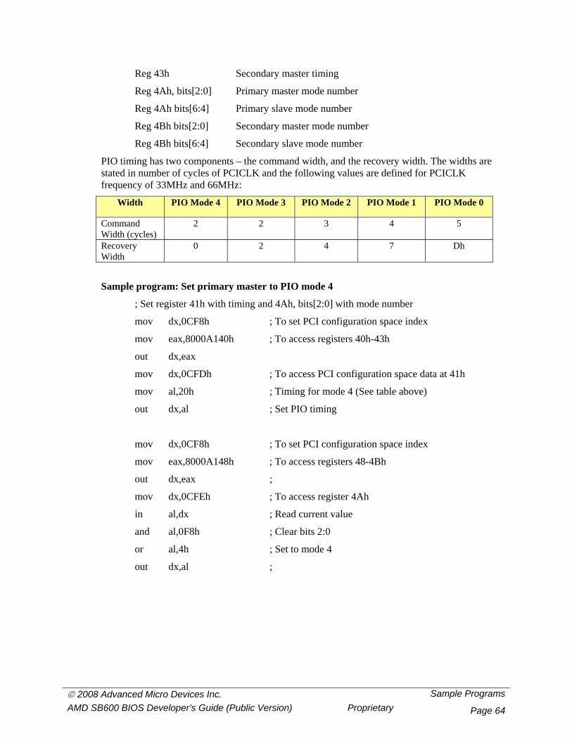
© 2008 Advanced Micro Devices Inc. Sample Programs AMD SB600 BIOS Developer’s Guide (Public Version) Proprietary Page 64
Reg 43h Secondary master timing
Reg 4Ah, bits[2:0] Primary master mode number
Reg 4Ah bits[6:4] Primary slave mode number
Reg 4Bh bits[2:0] Secondary master mode number
Reg 4Bh bits[6:4] Secondary slave mode number
PIO timing has two components – the command width, and the recovery width. The widths are stated in number of cycles of PCICLK and the following values are defined for PCICLK frequency of 33MHz and 66MHz:
Width PIO Mode 4 PIO Mode 3 PIO Mode 2 PIO Mode 1 PIO Mode 0
Command Width (cycles)
2 2 3 4 5
Recovery Width
0 2 4 7 Dh
Sample program: Set primary master to PIO mode 4
; Set register 41h with timing and 4Ah, bits[2:0] with mode number
mov dx,0CF8h ; To set PCI configuration space index
mov eax,8000A140h ; To access registers 40h-43h
out dx,eax
mov dx,0CFDh ; To access PCI configuration space data at 41h
mov al,20h ; Timing for mode 4 (See table above)
out dx,al ; Set PIO timing
mov dx,0CF8h ; To set PCI configuration space index
mov eax,8000A148h ; To access registers 48-4Bh
out dx,eax ;
mov dx,0CFEh ; To access register 4Ah
in al,dx ; Read current value
and al,0F8h ; Clear bits 2:0
or al,4h ; Set to mode 4
out dx,al ;

© 2008 Advanced Micro Devices Inc. Sample Programs AMD SB600 BIOS Developer’s Guide (Public Version) Proprietary Page 65
14.3.2 Multiword DMA Settings
IDE multiword DMA setting is done through registers 44h to 47h. The timing for the multiword DMA modes has two components – the command width, and the recovery width.
Width MW DMA Mode 2 MW DMA Mode 1 MW DMA Mode 0 Command Width (Cycles) 2h 2h 7h Recovery Width (Cycles) 0h 1h 7h
The register assignment is as follows:
Register 44h Primary slave MW DMA timing
Register 45h Primary master MW DMA timing
Register 46h Secondary slave MW DMA timing
Register 47h Secondary master MW DMA timing
Sample Program:
The following Assembly language code sample programs the secondary master to multiword DMA Mode 2 (i.e., it programs register 47h to 20h).
mov dx,0CF8h ; To access PCI configuration space, index register
mov eax,8000A144h ; Device 14h, function 1, registers 44h-47h
out dx,eax ;
mov dx,0CFFh ; To access PCI register 47h
mov al,20h ; Timing for MW DMA Mode 2
out dx,al
14.3.3 UDMA Mode Settings
IDE UDMA enable/disable is set through register 54h, and the UDMA mode is set through the registers 56h-57h. The register assignments are as follows:
Register 54h, bit[0] Primary master. 1 = Enable, 0 = Disable
Register 54h, bit[1] Primary slave. 1 = Enable, 0 = Disable
Register 54h, bit[2] Secondary master. 1 = Enable, 0 = Disable
Register 54h, bit[3] Secondary slave. 1 = Enable, 0 = Disable
Register 56h, bits[2:0] Primary master UDMA mode, 000b-110b
Register 56h, bits[6:4] Primary slave UDMA mode, 000b-110b
Register 57h, bits[2:0] Secondary master UDMA mode, 000b-110b
Register 57h, bits[6:4] Secondary slave UDMA mode, 000b-110b

© 2008 Advanced Micro Devices Inc. Sample Programs AMD SB600 BIOS Developer’s Guide (Public Version) Proprietary Page 66
Sample Program
The sample program below sets the primary slave to UDMA mode 5:
push eax
push dx
; For primary slave, set register 56h, bits [6:4] to 5 for UDMA mode 5
mov dx,0CF8h ; To access PCI configuration space of IDE controller
mov eax,8000A154h ; Device 14h, function 1, register space 54h – 57h
out dx,eax ;
mov dx,0CFEh ; To access register 56h
in al,dx ; Current value of register 56h
and al,8Fh ; Clear bits 6:4.
or al,50h ; Set UDMA 5 mode for primary slave.
out dx,al
; Enable primary slave UDMA mode in register 54h, bit 1,
mov dx,CFCh ; To access register 54h
in al,dx ; Current value of register 54h
or al,02h ; Set bit 1
out dx,al
pop dx
pop eax
ret
14.3.4 IDE Channel Disable
To disable an IDE channel, the BIOS must:
1. Set IDE channel programmable logic enable bit in Reg09h.
2. Set IDE channel disable bit in Reg48h to disable IDE channel.
Note: No IDE I/O port access is allowed between step (1) and step (2). It is recommended that the BIOS execute step (2) immediately after step (1). There should be no ‘in’ instruction between two ‘out’ instructions to register 09h and 48h.
After the IDE disable sequence, the IDE channel programmable logic enable bit will be cleared automatically.
Sample program: Disable secondary channel
; Read current register 48h-49h on IDE controller
push eax push bx

© 2008 Advanced Micro Devices Inc. Sample Programs AMD SB600 BIOS Developer’s Guide (Public Version) Proprietary Page 67
push dx mov eax,8000A148h ; To modify register 48h on the IDE controller mov dx,0CF8h ; PCI index register out dx,eax ; Set index for register 48h-4Bh mov dx,0CFCh ; Set PCI data register for 48h in ax,dx ; Read register 49h
mov bx,ax ; Save current 48h-49h registers ; Unlock the IDE controller to be enabled/disabled bit mov eax,8000A108h ; To write to PCI register 08h on IDE controller mov dx,0CF8h ; PCI index register out dx,eax ; Set index for registers 08h – 0Bh mov dx,0CFDh ; To read register 09h in al,dx ; Read register 09h or al,08h ; Set bit 3 to enable secondary channel program out dx,al ; Write back to register ; Disable the secondary IDE channel. The register 48h-49h is saved in BX mov eax,8000A148h ; To modify register 48h on the IDE controller mov dx,0CF8h ; PCI index register out dx,eax ; Set index for register 48h-4Bh mov dx,0CFCh ; Set PCI data register for 49h or bx,0100h ; Set bit 8 of 48h mov ax,bx out dx,ax
; Lock in the secondary channel to enable/disable bit mov eax,8000A108h ; To write to PCI register 08h on IDE controller mov dx,0CF8h ; PCI index register out dx,eax ; Set index for registers 08h – 0Bh mov dx,0CFDh ; To read register 09h in al,dx ; Read register 09h and al,0F7h ; Clear bit 3 to enable secondary channel program out dx,al ; Write back to register pop dx pop bx pop eax
; End of secondary channel disable

© 2008 Advanced Micro Devices Inc. Sample Programs AMD SB600 BIOS Developer’s Guide (Public Version) Proprietary Page 68
14.3.5 IDE Channel Enable
The primary IDE channel is enabled as power-on default. To enable an IDE channel after they have been disabled, the BIOS must:
1. Set the IDE channel programmable logic enable bit in Reg09h.
2. Clear the IDE channel disable bit in Reg48h to enable the IDE channel.
Note: No IDE I/O port access is allowed between step (1) and step (2). It is recommended that the BIOS execute step (2) immediately after step (1). There should be no ‘in’ instruction between two ‘out’ instructions to register 09h and 48h.
Sample program: Enable Primary IDE channel
; Read current register 48h-49h on IDE controller
push eax push bx push dx mov eax,8000A148h ; To modify register 48h on the IDE controller mov dx,0CF8h ; PCI index register out dx,eax ; Set index for register 48h-4Bh mov dx,0CFCh ; Set PCI data register for 48h in ax,dx ; Read register 49h
mov bx,ax ; Save current 48h-49h registers ; Unlock the IDE controller to enable/disable bit mov eax,8000A108h ; To write to PCI register 08h on IDE controller mov dx,0CF8h ; PCI index register out dx,eax ; Set index for registers 08h – 0Bh mov dx,0CFDh ; To read register 09h in al,dx ; Read register 09h or al,02h ; Set bit 1 to enable primary channel program out dx,al ; Write back to register ; Enable the primary IDE channel. The register 48h-49h is saved in BX mov eax,8000A148h ; To modify register 48h on the IDE controller mov dx,0CF8h ; PCI index register out dx,eax ; Set index for register 48h-4Bh mov dx,0CFCh ; Set PCI data register for 49h and bx,0FFFEh ; Clear bit 0 of 48h mov ax,bx out dx,ax
; Lock in the primary channel to enable/disable bit

© 2008 Advanced Micro Devices Inc. Sample Programs AMD SB600 BIOS Developer’s Guide (Public Version) Proprietary Page 69
mov eax,8000A108h ; To write to PCI register 08h on IDE controller mov dx,0CF8h ; PCI index register out dx,eax ; Set index for registers 08h – 0Bh mov dx,0CFDh ; To read register 09h in al,dx ; Read register 09h and al,0FBh ; Clear bit 1 to enable primary channel program out dx,al ; Write back to register pop dx pop bx pop eax ; End of primary channel enable
14.4 USB Controller Reset at Hard Reset
This USB controller reset sequence is not required for SB600
14.5 Clock Throttling
The SB600 has a register for setting clock duty cycle (throttling). The CLKVALUE register is located in the ACPI region. Bit 4 of this register, when set to 1, enables clock throttling, while bits [3:1] select the duty cycle from 12.5% to 87.5%, in seven steps of 12.5% each.
The address of ACPI CLKVALUE register is at PM IO location (Index/Data through 0CD6h/0CD7h) index 26h and 27h.
CLKVALUE register
Bit 4 Bits[3:1] Duty Cycle
0 x x x 100%
1 0 0 0 Invalid
1 0 0 1 12.5%
1 0 1 0 25%
1 0 1 1 37.5%
1 1 0 0 50%
1 1 0 1 62.5%
1 1 1 0 75%
1 1 1 1 87.5%
Sample program: Clock throttling
ClockThrottleExample proc near
push ax ; Save registers used by this routine
push dx

© 2008 Advanced Micro Devices Inc. Sample Programs AMD SB600 BIOS Developer’s Guide (Public Version) Proprietary Page 70
; Get ACPI CLKVALUE register address from PM IO index 26h and 27h
mov dx,0CD6h ; Set the PM IO register index
mov al, 27h ; Index = High byte, ACPI clock address
out dx,al
mov dx,0CD7h ; Get PM IO register data
in al,dx ; High byte of ACPI clock address
mov ah,al ; Save High byte of address
mov dx,0CD6h ; Set the PM IO register index
mov al, 26h ; Index = Low byte, ACPI clock address
out dx,al
mov dx,0CD7h ; Get PM IO register data
in al,dx ; Low byte of ACPI clock address
mov dx,ax ; dx = CLKVALUE address
; Enable throttling (set bit 4=1) and set duty cycle to 50%,(Set bits [3:1]=100b
in al,dx ; Read current CLKVALue
and al,0E1h ; Keep the unused bits
or al,18h ; Set bit 4 to enable and bits [3:1]=100b for 50%
out dx,al ; Write new throttling value
pop dx ; Restore registers used by this routine
pop ax
ret
ClockThrottleExample endp

© 2008 Advanced Micro Devices Inc. Sample Programs AMD SB600 BIOS Developer’s Guide (Public Version) Proprietary Page 71
14.6 Lid Switch
The Lid Switch programming is implementation specific. In a typical implementation the output of the debounced lid switch is connected to one of the Gevent or GPM pins. The Gevent and GPM pins can trigger the ACPI event, and the trigger polarity is programmable through the Southbridge register. The Gevent and GPM pins are in S5 plane and hence can trigger the event in S5 state.
14.6.1 Lid Switch Hardware Connection
This sample program assumes that the SB600 ExtEvent0 pin is connected to the lid switch.
14.6.2 Associated Registers
The registers associated with ExtEvent0 are:
ExtEvent0 Trigger polarity at PMIO index 37h, bit 0. Set to 1 for rising edge trigger and clear to 0 for falling edge trigger. (Default = 0)
ExtEvent0 signal to S5 region at PMIO index 78h bit 2. Set to 1 for S5 plane. (Default =1).
ExtEvent0 set as ACPI function at Device 14h, function 0, register 66h, bit 6. Set to 1 to enable ExtEvent0 as ACPI function. ExtEvent0 is a multi function pin and it must be set for the ACPI function.
ExtEvent0 ACPI event enable. This register is part of ACPI GPE0 block. The address is BIOS implementation specific (refer to PMIO register at index 28h and 29h). For this sample program, the ACPI GPE0 block starts at 820h. ExtEvent0 is bit 16 of the block.
14.6.3 BIOS Initialization.
The registers must be initialized during the boot up process. The order of initialization is not critical. The initialization may be done in the BIOS at any stage of the boot up process after GPE0 block is set in PMIO registers 28h,29h).
; Select EvtEvent0 as ACPI pin by setting device 14h, function 0, register 66h, bit 6 = 1
mov eax,8000A064h ; To access registers 64h-67h
mov dx,0CF8h ; PCI index register
out dx,eax
mov dx,0CFEh ; PCI data register for 66h
in al,dx ; Read current value
or al,40h ; Set bit 6
out dx,al
; Program ExtEvent0 trigger polarity to 0 (falling edge trigger ) to indicate lid open .
; Clear PMIO register 37h, bit 0 = 0

© 2008 Advanced Micro Devices Inc. Sample Programs AMD SB600 BIOS Developer’s Guide (Public Version) Proprietary Page 72
mov dx,0CD6h ; PMIO index
mov al,37h ;
out dx,al ; Set PMIO index
mov dx,0CD7h ; PMIO data
in al,dx ; Read current value
and al,0Feh ; Falling edge trigger (on closing the lid)
out dx,al
; Enable ExtEvent bit in ACPI GPE0 enable block.
mov dx,824h ; GPE0 enable is offset 4 of GPE0 block
in eax,dx ; Read GPE0 block
or eax,0100h ; Set bit 16, ExeEvent0 enable
out dx,eax
; Enable ExtEvent0 to S5 plane. This step is optional as the bit is set by default.
mov dx,0CD6h ; PMIO index
mov al,78h ; S5 plane enable register
out dx,al
mov dx,0CD7h ; PMIO data register
in al,dx ; Read current register
or al,04h ; ExtEvent0 to S5 plane
out dx,al
14.6.4 ACPI Programming
The ASL code defines the following:
The operation region where the lid polarity resides in address space. In our example that is at PMIO register 37h, bit 0.
A device called \_SB.LID with HID of PNP0C0D.
Method _LID to return current lid status.
A _PRW package that defines wake from S4 states (which includes wake from S1, S3 also).
Event handler _GPE.

© 2008 Advanced Micro Devices Inc. Sample Programs AMD SB600 BIOS Developer’s Guide (Public Version) Proprietary Page 73
///////////////////////////////////////////////////////////////////////////////////////////////////////////
//Code for Lid Switch control. //
// This code is based on Lid switch connected to ExtEvent0. //
// ExtEvent0 causes ACPI event 16 or 0x10 //
// ExtEvent0 trigger polarity is controlled by GPIO register 37h, bit 0 //
// PMIO reg 37h bit 0 = 0 Trigger ACPI event on falling edge //
// PMIO reg 37h bit 0 = 1 Trigger ACPI event on rising edge //
// //
// In addition, ExtEvent0 needs to be enabled for ACPI event. Device 14h, //
// function 0, register 66h, bit 6 should be set to 1 in the BIOS //
// initialization code for ExtEvent0 to be ACPI event causing SMI. //
///////////////////////////////////////////////////////////////////////////////////////// //
OperationRegion (PMIO, SystemIO, 0xCD6, 0x2)
Field (PMIO, ByteAcc, NoLock, Preserve)
{
INPM,8,
DAPM,8
}
IndexField (INPM, DAPM, ByteAcc, NoLock, Preserve) //R07
{
Offset(0x37), // To change trigger polarity for ExtEvent0
LPOL,1, // 1 = rising edge, 0 = falling edge
//
} //end of indexed field
// Define the Lid Device. Lid switch is connected to ExtEvent0 which
// causes ACPI event 16 (0x10)
Device(\_SB.LID)
{
Name(_HID, EISAID("PNP0C0D"))
Method(_LID)
{

© 2008 Advanced Micro Devices Inc. Sample Programs AMD SB600 BIOS Developer’s Guide (Public Version) Proprietary Page 74
if(LPOL){Return(0x00)} // Lid is closed
else {Return(0x1)} // Lid is open
}
Name(_PRW, Package(2)
{ 0x10, 0x03} // ACPI event 0x10 can wake-up from S3
)
}
//ACPI event
Scope(\_GPE)
{ Method(_L10)
{
Not(LPOL, LPOL) // Reverse the polarity from sleep to wake and vice versa
Notify(\_SB.LID, 0x80) // Notify the OS that status has changed.
}
}
14.7 SATA Hot Plug Sample Program
Scope(\_GPE)
{
Method(_L1F,0x0,Notserialized) // GPE0 Block bit 31 is used for SATA //hot plug
{
sleep(2000)
// For SATA at Bus 0, Device 12h, Function 0, channel 0 device
// Check if change in the status of the Serial ATA PHY
if(\_SB_.PCI0.SATA.STA0) { // BAR5, offset 10ah, bit0
Notify(\_SB.PCI0.SATA.PRID.P_D0, 0x00)
sleep(2000)
Notify(\_SB.PCI0.SATA.PRID, 0x01)
sleep(2000)
store(\_SB_.PCI0.SATA.STA0,\_SB_.PCI0.SATA.STA0) //Clear Status of // master SATA
}

© 2008 Advanced Micro Devices Inc. Sample Programs AMD SB600 BIOS Developer’s Guide (Public Version) Proprietary Page 75
// For SATA at Bus 0, Device 12h, Function 0, channel 1 device
// Check if change in the status of the Serial ATA PHY
if(\_SB_.PCI0.SATA.STA1) { // BAR5, offset 18Ah, bit 0
Notify(\_SB.PCI0.SATA.SECD.S_D0, 0x00)
sleep(2000)
Notify(\_SB.PCI0.SATA.SECD, 0x01)
sleep(2000)
store(\_SB_.PCI0.SATA.STA1,\_SB_.PCI0.SATA.STA1) //clear Status // of slave SAT
}
// For SATA at Bus 0, Device 11h, Function 0 , channel 0 device
// Check if change in the status of the Serial ATA PHY
if(\_SB_.PCI0.SAT2.STA0){ //BAR5, offset 10ah, bit0
Notify(\_SB.PCI0.SAT2.PRID.P_D0, 0x00)
sleep(2000)
Notify(\_SB.PCI0.SAT2.PRID, 0x01)
sleep(2000)
store(\_SB_.PCI0.SAT2.STA0,\_SB_.PCI0.SAT2.STA0) //clear Status // of master SATA
}
// For SATA at Bus 0, Device 11h, Function 0, channel 1 device
// Check if change in the status of the Serial ATA PHY
if(\_SB_.PCI0.SAT2.STA1) { //BAR4, offset 18Ah, bit 0
Notify(\_SB.PCI0.SAT2.SECD.S_D0, 0x00)
sleep(2000)
Notify(\_SB.PCI0.SAT2.SECD, 0x01)
sleep(2000)
store(\_SB_.PCI0.SAT2.STA1,\_SB_.PCI0.SAT2.STA1) //clear // Status of slave SAT
}
} // End of Method(_L1F)
} // End of Scope(\_GPE)

© 2008 Advanced Micro Devices Inc. Sample Programs AMD SB600 BIOS Developer’s Guide (Public Version) Proprietary Page 76
Scope(\_SB_.PCI0.SATA) // Bus 0, Device 12h, Function 0
{
OperationRegion(BAR5, SystemMemory, 0xFFF80000, 0x1000) // The // address should be replaced by the BIOS
Field(BAR5, AnyAcc, NoLock, Preserve)
{
Offset(0x104), // Channel 0
CSTX, 1, // Device detected but no communication with Phy
CST0, 1, // Communication with Phy established. (Physgood)
Offset(0x10A), // Channel 0
STA0, 1, // Change in Phy status
Offset(0x184), // Channel 1
CSTY, 1, // Device detected but no communications with Phy
CST1, 1, // Communication with Phy established (Physgood)
Offset(0x18A), // Channel 1
STA1, 1, // Changes in Phy status
} // End of Field(BAR5 ……)
Method(_INI) { // For Bus 0, Device 12h, Function 0
if(\_SB_.PCI0.SATA.STA0){
store(\_SB_.PCI0.SATA.STA0,\_SB_.PCI0.SATA.STA0) //clear channel // 0 SATA status
}
if(\_SB_.PCI0.SATA.STA1){
store(\_SB_.PCI0.SATA.STA1,\_SB_.PCI0.SATA.STA1) //clear channel // 1 SATA status
}
} // End of Method (_INI)
Device(PRID) {
Name(_ADR, 0) // IDE Primary Channel

© 2008 Advanced Micro Devices Inc. Sample Programs AMD SB600 BIOS Developer’s Guide (Public Version) Proprietary Page 77
Device(P_D0) {
Name(_ADR, 0) // Drive 0 - Master
Method(_STA,0){
if (\_SB_.PCI0.SATA.CST0) { //If SATA detected
return(0x0f)
}
else {
return (0x00)
}
} End of Method (_STA )
} // End of P_D0
} // End of PRID
Device(SECD) {
Name(_ADR, 1) // IDE Secondary Channel
Device(S_D0) {
Name(_ADR, 0) // Drive 0 - Master
Method(_STA,0){
if (\_SB_.PCI0.SATA.CST1) { // If SATA detected
return(0x0f)
}
else {
return (0x00)
} /
} // End of Method (_STA)
} // End of S_D0
} // End of SECD
} // End of Scope(_SB.PCI0.SATA)

© 2008 Advanced Micro Devices Inc. Sample Programs AMD SB600 BIOS Developer’s Guide (Public Version) Proprietary Page 78
// Bus 0, Device 11h, Function 0
Scope(\_SB_.PCI0.SAT2)
{
OperationRegion(BAR5, SystemMemory, 0xFFF80000, 0x1000) // Replace //address in BIOS
Field(BAR5, AnyAcc, NoLock, Preserve)
{
Offset(0x104), //Channel 0
CSTX, 1, // Device detected but no communication with Phy
CST0, 1, // Communication with PHY established
Offset(0x10A), // Channel 0
STA0, 1, // Change in PHY status
Offset(0x184), // Channel 1
CSTY, 1, // Device detected but no communication // with PHY
CST1, 1, // Communication with PHY established
Offset(0x18A), //Channel 1
STA1, 1, // Change in PHY status
} // End of Field
Method(_INI) { // For Bus 0, Device 11h, Function 0
if(\_SB_.PCI0.SAT2.STA0){
store(\_SB_.PCI0.SAT2.STA0,\_SB_.PCI0.SAT2.STA0) // clear SATA // channel0 status
}
if(\_SB_.PCI0.SAT2.STA1){
store(\_SB_.PCI0.SAT2.STA1,\_SB_.PCI0.SAT2.STA1) // clear SATA // channel 1 status
}
} // End of Method(_INI)
Device(PRID) {

© 2008 Advanced Micro Devices Inc. Sample Programs AMD SB600 BIOS Developer’s Guide (Public Version) Proprietary Page 79
Name(_ADR, 0) // IDE Primary Channel
Device(P_D0) {
Name(_ADR, 0) // Drive 0 - Master
Method(_STA,0){
if (\_SB_.PCI0.SAT2.CST0) { // If SATA detected
return(0x0f)
}
else {
return (0x00)
}
} // End of Method(_STA)
} // End of P_D0
} // End of PRID
Device(SECD) {
Name(_ADR, 1) // IDE Secondary Channel
Device(S_D0) {
Name(_ADR, 0) // Drive 0 - Master
Method(_STA,0){
if (\_SB_.PCI0.SAT2.CST1) { // If SATA detected
return(0x0f)
}
else {
return (0x00)
}
} //End of Method(_STA)
} // End of S_D0
} // End of SECD
} // End of Scope(\_SB_.PCI0.SAT2)

© 2008 Advanced Micro Devices Inc. Sample Programs AMD SB600 BIOS Developer’s Guide (Public Version) Proprietary Page 80
14.8 Temperature Limit Shutdown through SMI#
The program to shut down the system when the temperature exceeds a pre-set limit requires the following:
1. A temperature sensing diode or thermistor positioned under the CPU socket. 2. A Super I/O device capable of monitoring the temperature and toggle an SMI# line
when the temperature exceeds the pre-set limit. 3. SMI programming in the SB600 to shut down the system.
The discussion below assumes that an ITE-8712 Super I/O is present in the system and is connected to the thermal diode to measure temperature-1 and temperature-2, and a thermistor to measure temperature-3. This code example shows thermal programming in the Super I/O, and SMI programming related to thermal shutdown.
Please refer to ITE-8712 Super I/O device manual for register details.
This code example assumes that the GP47 from Super I/O is connected to the ExtEvent1 pin on the SB600.
14.8.1 Setting Up ITE 8712 Super I/O Registers
ITE 8712 Super I/O registers are set during the boot up process through the BIOS program.
1. Set the Environmental Controller base address.
Select a base address in the I/O range which is not used by any device and is also accessible to the LPC. The address range is 8 bytes. In this example the I/O address 228h – 22Fh will be used. This address is set in Super I/O logical device 04h, registers 60h, and 61h. After the base address is set, the environment registers are accessed by index/data method at base address+5 as index, and base address+6 as data. For this example the index/data address would be 22Dh/22Eh. ; Define equates for index/data, shutdown temperature, and Super I/O access port.
Sensor_Port EQU 22Dh TemperatureLimit EQU 75
SuperIo_Config_Port EQU 2EH
call SuperIoEnterConfig ; Write 87h, 01h, 55h, 55h to SuperIo ; Enable the access to device 04 registers, i.e. set Super I/O address register to 04
; Device 04 is the Environment controller mov dx,2Eh ; Super I/O index mov al, 07h ; Register 07 is device select out dx,al mov dx,2Fh ; Super I/O data mov al, 04h ; Set register to 04 out dx,al

© 2008 Advanced Micro Devices Inc. Sample Programs AMD SB600 BIOS Developer’s Guide (Public Version) Proprietary Page 81
; Logical Device Number (LDN) is now set to 04. ; Set Base address to 0228h in registers 60h and 61h of this LDN = 04 ; Set MS byte of base address to 02h mov dx,2Eh mov dx,60h out dx,al mov dx,2Fh ; Super I/O index mov al,02h ; MS byte of 0228h out dx,al ; Set LS byte of the base address to 28h mov dx,2Eh mov dx,61h out dx,al mov dx,2Fh ; Super I/O index mov al,28h ; MS byte of 0228h out dx,al
; The environment (temperature, voltage etc.) registers can now be accessed ; through Base address + 5 (index), and base address + 6, i.e. 22Dh and 22Eh
mov ah, TemperatureLimit ; Selected through setup or OEM ; Set limit for 1st Thermistor ; Register 40h is for upper limit, register 41h is for lower limit ; If lower limit is set to 7Fh, then the temperature controller is in the comparator mode mov dx,Sensor_Port ; The register is written through index at 22Dh mov al,40h ; To set the upper limit out dx,al mov dx,Sensor_Port+1 ; The temperature value is written through 22Eh mov al,ah ; Get the Temperature upper limit out dx,al mov dx,Sensor_Port ; The register is written through index at 22Dh mov al,41h ; To set the lower limit out dx,al mov dx,Sensor_Port+1 mov al,7fh ; Lower limit of 7Fh to enable the comparator mode out dx,al ; Set limit for 2nd Thermistor

© 2008 Advanced Micro Devices Inc. Sample Programs AMD SB600 BIOS Developer’s Guide (Public Version) Proprietary Page 82
; Register 42h is for upper limit, register 43h is for lower limit ; If lower limit is 7Fh then it is comparator mode mov dx,Sensor_Port ; The register is written through index at 22Dh mov al,42h ; To set the upper limit out dx,al mov dx,Sensor_Port+1 ; The temperature value is written through 22Eh mov al,ah ; Get the Temperature upper limit out dx,al mov dx,Sensor_Port ; The register is written through index at 22Dh mov al,43h ; To set the lower limit out dx,al mov dx,Sensor_Port+1 ; The temperature value is written through 22Eh mov al,7fh ; For comparator mode out dx,al ; Set limit for 3rd Thermistor ; Register 44h is for upper limit, register 45h is for lower limit ; If lower limit is 7Fh then it is comparator mode mov dx,Sensor_Port ; The register is written through index at 22Dh mov al,44h ; To set the upper limit out dx,al mov dx,Sensor_Port+1 ; The temperature value is written through 22Eh mov al,ah ; Get the temperature upper limit out dx,al mov dx,Sensor_Port ; The register is written through index at 22Dh mov al,45h ; To set the lower limit out dx,al mov dx,Sensor_Port+1 ; The temperature value is written through 22Eh mov al,7Fh ; For comparator mode out dx,al ; Set Thermal out limit registers at 52h, 53h, 54h mov dx,Sensor_Port ; The register is written through index at 22Dh mov al,52h ; Thermal limit for diode 1 out dx,al mov dx,Sensor_Port+1 ; The temperature value is written through 22Eh mov al,ah ; Get temperature upper limit out dx,al mov dx,Sensor_Port ; The register is written through index at 22Dh mov al,53h ; Thermal limit for diode 2

© 2008 Advanced Micro Devices Inc. Sample Programs AMD SB600 BIOS Developer’s Guide (Public Version) Proprietary Page 83
out dx,al mov dx,Sensor_Port+1 ; The temperature value is written through 22Eh mov al,ah ; Get temperature upper limit out dx,al mov dx,Sensor_Port ; The register is written through index at 22Dh mov al,54h ; Thermal limit for thermistor 3 out dx,al mov dx,Sensor_Port+1 ; The temperature value is written through 22Eh mov al,ah ; Get temperature upper limit out dx,al ; Read status from register 03 to clear the status mov dx,Sensor_Port ; The register is read through index at 22Dh mov al,03h out dx,al mov dx,Sensor_Port+1 ; The register is read through data at 22Eh in al,dx ; Enable Interrupt/SMI# register at 00. mov dx,Sensor_Port ; The register is written through index at 22Dh mov al,00h out dx,al mov dx,Sensor_Port+1 ; The register is written through data at 22Eh in al,dx or al,07h ; Enable IRQ, SMI# and enable monitoring out dx,al ; In logical device 7, set SMI registers, thermal out register, ; and enable the SMI. ; 1. Set logical device to 7 mov al,07h mov dx,SuperIo_Config_Port out dx,al mov al,07h inc dx out dx,al ; 2. Set SMI pin to GP47 ( 00 100 111 = 27h) in reg 0f4h

© 2008 Advanced Micro Devices Inc. Sample Programs AMD SB600 BIOS Developer’s Guide (Public Version) Proprietary Page 84
; Register F4 is SMI mapping register mov al,0f4h mov dx,SuperIo_Config_Port out dx,al inc dx mov al,27h out dx,al ; 3. Set Thermal output to GP47(00 100 111 = 27h) in reg 0F5h ; Register 0F is thermal mapping register mov al,0f5h mov dx,SuperIo_Config_Port out dx,al inc dx mov al,27h out dx,al ; Enable generation of SMI# due to environment condition mov al,0f0h mov dx,SuperIo_Config_Port out dx,al inc dx in al,dx or al,10h out dx,al ; Set GP47 as general purpose pins ; Registers 25h and 28 are global access registers ; Select IRTX/GP47 as GP47 mov al,028h ; For GP-47 mov dx,SuperIo_Config_Port out dx,al inc dx in al,dx or al,80h out dx,al call SuperioExitConfig ; Write 02, 02 to Super IO

© 2008 Advanced Micro Devices Inc. Sample Programs AMD SB600 BIOS Developer’s Guide (Public Version) Proprietary Page 85
14.8.2 Initialize Southbridge Registers for SMI#
; Enable the base address range (228h-22Fh) in the LPC register. ; Address range 228h-22Fh is enabled in LPC Device 14h, function 3, Register 45h, bit 1
mov dx,0CF8h ; PCI device access index register mov eax,8000A344h ; Device 14h, function 3, registers 44h-47h out dx,eax mov dx,0CFDh ; To access register 45h in al,dx ; Read register 45h or al,02h ; Set bit 1 out dx,al ; Configure ExtEvent1 for SMI#. ExtEvent1 is configured through PMIO ; register 32h bit 3:2 = 00 mov dx,0cd6h mov al,32h out dx,al mov dx,0cd7h in al,dx and al,0f3h ; Clear bits 3:2 or al,04h ; Set [3:2] = 01 for SMI out dx,al ; Set ExtEvent1 for SMI, negative edge through PMIO register 37h, bit 1 = 0 mov dx,0cd6h mov al,37h out dx,al mov dx,0cd7h in al,dx and al,0fdh ; Clear bit 1 for Negative edge out dx,al ; Also set PMIO register 04 to enable ExtEvent1 for SMI mov dx,0cd6h mov al,04h out dx,al mov dx,0cd7h in al,dx or al,02h out dx,al ; End of temperature setting program.

© 2008 Advanced Micro Devices Inc. Sample Programs AMD SB600 BIOS Developer’s Guide (Public Version) Proprietary Page 86
14.8.3 SMI Programming to Shut Down the System
The SMI programming should shut down the system when the line connected to Super I/O for temperature over run is set.
; Check ExtEvent1 status. The ExtEvent1 status is on the PMIO register 07h, bit 1
mov dx,0cd6h mov al,07h out dx,al mov dx,0cd7h in al,dx test al,02h ; Bit 1 for ExtEvent1 jnz ShutDownFromTalert ; ExtEvent1 is set, shut down
; Check alternate ExtEvent 1 status
mov dx,0cd6h mov dl,3ah out dx,al mov dx,0cd7h in al,dx test al,02h jz NoShutDown
ShutDownFromTalert: mov dx,PM1a_CNT_BLK+1 mov al,34h ; Set S5 status out dx,al jmp $ NoShutDown: ; Continue with rest of the SMI routine.

© 2008 Advanced Micro Devices Inc. Sample Programs AMD SB600 BIOS Developer’s Guide (Public Version) Proprietary Page 87
14.9 Sleep Trap through SMI#
This sample code provides an SMI# routine to develop some software workarounds or debugging functions before the system goes into ACPI sleep state.
14.9.1 Enable Sleep SMI# in ACPI ASL code
The following example implements Sleep SMI Control Register enable by the ASL code _PTS method.
Method(_PTS, 1) { Store(One, \_SB.PCI0.SMBS.SLPS) PTS(Arg0) Store(0, Index(WAKP,0)) // Clear Wake up package. Store(0, Index(WAKP,1)) // Clear Wake up package. }
OperationRegion (PMIO, SystemIO, 0xCD6, 0x2) Field (PMIO, ByteAcc, NoLock, Preserve) {
INPM,8, DAPM,8
} IndexField (INPM, DAPM, ByteAcc, NoLock, Preserve) //R07 {
Offset(0x00), ,1, TM1E,1, // Set to 1 to enable SMI# when PM_TIMER1 expires TM2E,1, // Set to 1 to enable SMI# when PM_TIMER2 expires Offset(0x01), ,1, TM1S,1, // SB sets this bit to indicate that PM_TIMER1 has expired TM2S,1, // SB sets this bit to indicate that PM_TIMER2 has expired Offset(0x04), ,7, SLPS,1, // Set this bit to enable SLP2SMI Offset(0x1C), ,3, MKME,1, // PI3E,1, // I2E,1, // PI1E,1, // PI0E,1, // Offset(0x1D), ,3, MKMS,1, // PI3S,1, // PI2S,1, //

© 2008 Advanced Micro Devices Inc. Sample Programs AMD SB600 BIOS Developer’s Guide (Public Version) Proprietary Page 88
PI1S,1, // PI0S,1, // Offset(0x55), SPRE,1, // Offset(0x68), ,3, TPDE,1, // ,1
} //end of indexed field
14.9.2 Sleep Trap SMI Routine
The following example implements the Sleep Trap SMI# routine.
SLPSMI_HANDLER_FAR PROC FAR PUBLIC ; Read PM1_CNT to get sleep type
mov dx, PM_BASE_ADDRESS + SB_PM_IO_PM1_CTRL; (PM1_CNT 04h) in ax, dx and ax, PM1_CNT_SLP_TYPE shr ah, 2 dec ah ; For Table from 0 movzx bx, ah shl bx, 1 add bx, offset cs:ACPISleepTrapTable mov bx, cs:[bx]
SleepTrapPatch: cmp word ptr cs:[bx], 0ffffh je short SleepTrapPatchDone push bx call word ptr cs:[bx] pop bx inc bx inc bx jmp short SleepTrapPatch
SleepTrapPatchDone: ; Disable SLP2SMI
mov ah, SB_PMU_REG_04 ; PMIO_REG.04h[7] = SLP2SMI Enable call read_io_pmu and al, NOT BIT7 ; Disable SLP2SMI
call write_io_pmu ; Clear SLP2SMI Status bit
mov ah, SB_PMU_REG_07 ; PMIO_REG.07h[7] = SLP2SMI Status call read_io_pmu call write_io_pmu ; Write 1 to clear SLP2SMI status
; Write SLP_EN to put SB into sleep mov dx, PM_BASE_ADDRESS + SB_PM_IO_PM1_CTRL ; PM1_CNT 04h in ax, dx or ax, Bit13 ; PM1_CNT_SLP_EN out dx, ax ; This puts SB to sleep state
ret

© 2008 Advanced Micro Devices Inc. Sample Programs AMD SB600 BIOS Developer’s Guide (Public Version) Proprietary Page 89
SLPSMI_HANDLER_FAR ENDP ACPISleepTrapTable label byte
dw offset cs:ACPISleepTrapS1 dw offset cs:ACPISleepTrapS2 dw offset cs:ACPISleepTrapS3 dw offset cs:ACPISleepTrapS4 dw offset cs:ACPISleepTrapS5
ACPISleepTrapS1 label byte dw offset cs:OemACPISleepTrapS1 dw 0FFFFh
ACPISleepTrapS3 label byte dw offset cs:Port80_Enabled dw offset cs:OemACPISleepTrapS3 dw 0FFFFh
ACPISleepTrapS4 label byte dw offset cs:OemACPISleepTrapS4
dw 0FFFFh ACPISleepTrapS5 label byte
dw offset cs:OemACPISleepTrapS5 dw 0FFFFh
14.10 HD Audio – Detection and Configuration
:******************************************************************************************** ; Equates for HD Audio detection ATI_PCIE_BAR3 EQU 0E0000000h ; NB BAR3 base at Bus-0,Dev-0, func-0,Reg 1ch ATI_AZALIA_BUS_DEV_FUN EQU (14h) shl 3 + 2 ATI_SMBUS_BUS_DEV_FUN EQU (14H) shl 3 + 0 ATI_AZALIA_ID EQU 0437b1002h ATI_AZALIA_ExtBlk_Addr EQU 0F8h ATI_AZALIA_ExtBlk_DATA EQU 0FCh ;************************************************************************ ; ATI_SB_Cfg_Azalia * ; * ; Configure HD Audios * ; * ; Input: EBP = 0 * ; ES = 0 * ; * ;************************************************************************ ATI_SB_Cfg_Azalia PROC NEAR

© 2008 Advanced Micro Devices Inc. Sample Programs AMD SB600 BIOS Developer’s Guide (Public Version) Proprietary Page 90
pushad ; OEM specific CMOS setup option to Auto/Disable/enable HD Audio mov ax,CMOS_Azalia_Option ; OEM specific call ReadCMOSOption ; OEM specific cmp ax,1 ; Is it disable? je DisableAzaliaController ; Jump for Disable HD Audio ; OEMs may have a CMOS setup option for HD Audio clock source. ; The options may be USB 48 MHz or HD Audio 48 MHz ; Device 14h, function 2, register 43h, bit 0 = 1 for HD Audio clock.
mov ax,CMOS_AZA_CLOCK ; OEM specific call ReadCMOSOption ; OEM specific cmp ax,1 ; Is it HD Audio clock at 48 MHz jne @f ; Jump for USB 48 MHz clock or Byte PTR es:[ebp+ATI_PCIE_BAR3+ATI_AZALIA_BUS_DEV_FUN shl 12 + 043h], BIT0 ; Enable xAz48Mhz pin as clock source of 48Mhz call ATI_fixed_delay_1ms_far ; Wait 1ms @@: ; OEM may have CMOS setup for HD Audio snoop (0= Disable, 1=Enable) ; Device 14h, function 2, register 42, bits 1 and 0 control snoop option mov ax,CMOS_AZA_SNOOP ; OEM specific call ReadCMOSOption ; OEM specific cmp ax,1 ; Snoop enabled? jne @f ; Jump for disabled or Byte PTR es:[ebp+ATI_PCIE_BAR3+ATI_AZALIA_BUS_DEV_FUN shl 12 + 042h], BIT1 ; Enable Snoop @@: ; Set subsystem ID at device 14h, function 2, register 2ch mov Dword PTR es:[ebp+ATI_PCIE_BAR3+ATI_AZALIA_BUS_DEV_FUN shl 12 +2Ch], \
ATI_AZALIA_ID ; Write subsystem ID ; Get HD Audio controller’s memory mapped configuration registers in EBX mov ebx, Dword PTR es:[ebp+ATI_PCIE_BAR3+ATI_AZALIA_BUS_DEV_FUN shl 12 +10h] ; HD Audio port configuration through Extended registers. ; Extended registers are addressed as index/data through SMBUS(Dev 14h, func0) register 0F8h,
; and 0FCh ; Index 0 is Audio port configuration. 2 bit per port for total of 4 ports
mov Dword PTR es:[ebp+ATI_PCIE_BAR3+ATI_SMBUS_BUS_DEV_FUN shl 12 \
+ATI_AZALIA_ExtBlk_Addr], 0 ; Set index to 0
; First declare all the lines as GPIO lines by setting index 00 to all 1's. ; Then read the input status of these line at index 02 ; If the line is 1, it is guaranteed not to be HD Audio ; This step is necessary because after S4 resume from ring, the AC-97 gives same status as HD Audio

© 2008 Advanced Micro Devices Inc. Sample Programs AMD SB600 BIOS Developer’s Guide (Public Version) Proprietary Page 91
mov Byte PTR es:[ebp+ATI_PCIE_BAR3+ATI_SMBUS_BUS_DEV_FUN shl 12 \ +SB600_SMBUS_REGFC], 11111111b ; Set to GPIO
call ATI_fixed_delay_1ms_far ; Wait 1ms mov ecx, dword PTR es:[ebp+ATI_PCIE_BAR3+ATI_SMBUS_BUS_DEV_FUN shl 12 \
+SB600_SMBUS_REGFC] shr ecx,10h mov di,cx ; Save GPIO lines status at di[7:0]
mov Byte PTR es:[ebp+ATI_PCIE_BAR3+ATI_SMBUS_BUS_DEV_FUN shl 12 \
+ATI_AZALIA_ExtBlk_DATA], 10101010b ; Set pin to HD Audio
; Interrupt routing table for HD Audio is at SMBUS ( Dev 14h, func 0) register 63h
mov Byte PTR es:[ebp+ATI_PCIE_BAR3+ATI_SMBUS_BUS_DEV_FUN shl 12 + 063h], 0 ; Set PCI routing to #INTA ; Attempt to exit the reset state. This is done by command to exit the reset state and waiting ; for status of ready to begin operation. mov ecx, 10 ; Make up to 10 attempt to exit reset state re_do_reset: and bx, BIT15+BIT14 ; Clear bit0-13 or Byte PTR ES:[ebx+08h], BIT0 ; Exit the reset state call ATI_fixed_delay_1ms_far ; Wait 1ms test Byte PTR ES:[ebx+08h], BIT0 ; Read of 1 = Ready to begin operation jnz @f ; Go if reset bit is set loop re_do_reset ; Wait until ready to begin operation jmp ATI_SB_Cfg_Azalia_exit ; Exit because reset bit can not be set ; Ready to begin operation. ; Check codecs present by examining memory mapped register (pointed by EBX) at 0Eh @@: call ATI_fixed_delay_1ms_far ; Wait 1ms mov al, Byte PTR ES:[ebx+0eh] ; State change status register and al, 0fh ; Bits 3:0 are for state change status jnz At_least_one_azalia ; Codec present
; Disable Azalia controller and leave
DisableAzaliaController:
; Clear memory access at PCI register 04 and Word PTR es:[ebp+ATI_PCIE_BAR3+ATI_AZALIA_BUS_DEV_FUN shl 12 +04h], 0 ; Disable HD Audio module through PMIO register 59h bit 3 mov dx,0cd6h ; PMIO index register mov al,59h ; Set PMIO index to 59h out dx,al ; mov dx,0cd7h ; PMIO data register in al,dx ; Read current data

© 2008 Advanced Micro Devices Inc. Sample Programs AMD SB600 BIOS Developer’s Guide (Public Version) Proprietary Page 92
not al, BIT3 ; Clear bit 3 to disable HD Audio out dx,al ; Output new data ; HD Audio port configuration through Extended registers. ; Extended registers are addressed as index/data through SMBUS(Dev 14h, func0) register 0F8h,
; and 0FCh ; Index 0 is Audio port configuration. 2 bit per port for total of 4 ports
mov Byte PTR es:[ebp+ATI_PCIE_BAR3+ATI_SMBUS_BUS_DEV_FUN shl 12 \
+ATI_AZALIA_ExtBlk_DATA], 01010101b ; Set pin routine to AC97 jmp ATI_SB_Cfg_Azalia_exit ; Audio codec present ; Register AL has codec present bit map in bits 3:0 ; Register EBX points to memory mapped configuration registers At_least_one_azalia: mov dl, al ; After resume from S4 through ring, the AC97 lines give same status as HD Audio
; It is necessary to remove HD Audio status from those bits. The AC-97 ring resume status is in register ; DI[3:0]
mov ax,di ; Get GPIO status and AC97 S4 ring wakeup mov ah,0fh ; To keep only bits 3:0 and al,ah ; Keep only bits 3:0 xor al,ah ; Invert the AC97 ring bits and dl,al ; Remove GPIO and AC-97 bits from HD Audio bits mov cl, 0 test_SDI: test dl, BIT0 ; Test for specific codec present jnz configure_Azalia_channel ; Jump, codec is present
; This specific codec is not present. Set pin config to AC97 ; This pin is set through index 0 of extended registers. ; The extended registes are accessed as index/data at SMBus (dev 14h, func 0) registers 0F8h/0FCh ; There are two bits per codec. Register CL has the codec number.
mov ah, 01b ; 01 = Set codec as AC97 shl ah, cl ; Move in the position for this codec shl ah, cl ; Two bits per codec mov al, 11b ; Mask for this codec shl al, cl ; Move it in the position for this codec shl al, cl ; Two bits per codec xor al, -1 ; Zero these two bits and Byte PTR es:[ebp+ATI_PCIE_BAR3+ATI_SMBUS_BUS_DEV_FUN shl 12 \
+ATI_AZALIA_ExtBlk_DATA], al ; Clear channel pin config or Byte PTR es:[ebp+ATI_PCIE_BAR3+ATI_SMBUS_BUS_DEV_FUN shl 12 \
+ATI_AZALIA_ExtBlk_DATA], ah ; Set channel pin config to AC97 jmp test_next_SDI

© 2008 Advanced Micro Devices Inc. Sample Programs AMD SB600 BIOS Developer’s Guide (Public Version) Proprietary Page 93
configure_Azalia_channel: call ATI_SB_Cfg_Azalia_Pin_CMD ; Configure this pin test_next_SDI: shr dl, 1 ; Get next codec present inc cl ; Update the codec Channel number cmp cl, 4 ; Completed all channels je re_do_clear_reset ; Yes, jump. Reset the controller and exit jmp test_SDI ; Do the next codec ; Reset the controller and wait till it enters reset state. re_do_clear_reset: and Byte PTR ES:[ebx+08h], NOT (BIT0) ; Controller transition to reset state test Byte PTR ES:[ebx+08h], (BIT0) ; Test the reset status. 0 = Controller in reset state jnz re_do_clear_reset ; If 1, wait to enter reset state ATI_SB_Cfg_Azalia_exit: popad ret ATI_SB_Cfg_Azalia ENDP ;******************************************************************************* ; ATI_SB_Cfg_Azalia_Pin_CMD * ; * ; Configure each codec pin * ; * ; Input: cl, = channel number * ; ebx = Memory mapped configuration register address * ; * ;******************************************************************************** ATI_SB_Cfg_Azalia_Pin_CMD PROC NEAR pushad
; OEM may have CMOS setup option for Pin Configuration (0= Disable, 1=Enable) mov ax CMOS_Pin_Config ; OEM specific call ReadCMOSOption ; OEM specific cmp ax,1
jne ATI_SB_Cfg_Azalia_Pin_CMD_exit ; Jump if Pin Configuration is disabled ; Set codec channel number in bits 31:28 ; Write command for ID read shl ecx, 28 mov eax, 0F0000h ; Read IDs command or eax, ecx mov Dword PTR ES:[ebx+60h], eax ; Immediate command output register

© 2008 Advanced Micro Devices Inc. Sample Programs AMD SB600 BIOS Developer’s Guide (Public Version) Proprietary Page 94
call ATI_SB_Cfg_Azalia_Delay ; About 30 uSec delay mov eax, Dword PTR ES:[ebx+64h] ; Immediate command input cmp eax, 010ec0880h ; Is it Realtec codec? jne ATI_SB_Cfg_Azalia_Pin_CMD_exit ; This routine works only with Realtec codec mov si, offset Azalia_Codec_Table_Start mov di, offset Azalia_Codec_Table_end ; Table end does not include front panel ; OEM may have a CMOS setup selection for Front panel audio (0=Auto, 1=Disable)
mov ax CMOS_Front_Panel ; OEM specific call ReadCMOSOption ; OEM specific
cmp ax,1 ; Front panel disable je loop_Immediat_Command_Output_Interface ; Jump for front panel disable
; Front panel option is Auto. GPIO9 detects the front panel audio in the SB600, and GPIO8 detects the front panel audio in SB460.
;Check whether SB460?Call DetectSB460 Jz SB460_Chip ;jmp if SB460 ;Control comes here if SB600
; Set GPIO9 as input through SMBus (Dev 14h, func 0) register A9h, bit 5 ; Read GPIO9 through SMBus (Dev 14h, func 9) register AAh, bit 5 or Byte PTR es:[ebp+ATI_PCIE_BAR3+ATI_SMBUS_BUS_DEV_FUN shl 12 + 0A9h], BIT5 ; Set GPIO9 Input test Byte PTR es:[ebp+ATI_PCIE_BAR3+ATI_SMBUS_BUS_DEV_FUN shl 12 + 0AAh], BIT5 ; GPIO9 0:connected 1:not jmp DetectFrontPanelAudio SB460_Chip:
;Control comes here if SB460 ; Set GPIO8 as input through SMBus (Dev 14h, func 0) register A9h, bit 4 ; Read GPIO8 through SMBus (Dev 14h, func 9) register AAh, bit 4 or Byte PTR es:[ebp+ATI_PCIE_BAR3+ATI_SMBUS_BUS_DEV_FUN shl 12 + 0A9h], BIT4 ; Set GPIO8 Input test Byte PTR es:[ebp+ATI_PCIE_BAR3+ATI_SMBUS_BUS_DEV_FUN shl 12 + 0AAh], BIT4 ; GPIO8 0:connected 1:not DetectFrontPanelAudio: jnz loop_Immediat_Command_Output_Interface ; Jump, Front Panel audio is not present ; Front panel audio is present. Extend the end pointer to include front panel commands mov di, offset Azalia_Codec_Table_FP_Enable_end ; Write the codec commands loop_Immediat_Command_Output_Interface: cmp si, di ; End of table? je ATI_SB_Cfg_Azalia_Pin_CMD_exit ; Jump at the end of the command test_again: test Byte PTR ES:[ebx+68h], BIT0 ; Immediate command status register

© 2008 Advanced Micro Devices Inc. Sample Programs AMD SB600 BIOS Developer’s Guide (Public Version) Proprietary Page 95
jnz test_again ; If bit 0 == 1, codec is not ready for command mov eax, cs:[si] ; Get the command from the table or eax, ecx ; Add codec number 0 to 3 mov Dword PTR ES:[ebx+60h], eax ; Write immediate command call ATI_SB_Cfg_Azalia_Delay ; About 30 uSec delay add si, 4 ; Update the pointer jmp loop_Immediat_Command_Output_Interface ; Next command ATI_SB_Cfg_Azalia_Pin_CMD_exit: popad ret ATI_SB_Cfg_Azalia_Pin_CMD ENDP ;************************************************************************ : ATI_SB_Cfg_Azalia_Delay * ; * ; Wait about 30 uSec * ; * : Input : None * ;************************************************************************ ATI_SB_Cfg_Azalia_Delay PROC NEAR push cx mov cx, 4 call ATI_fixed_delay_far ; Wait approx cx * 7 uSec pop cx ret ATI_SB_Cfg_Azalia_Delay ENDP ;*********************************************************************** ; ATI_Fixed_delay_1ms_FAR * ; * ; Delay for approx 1 mSec * ; * ; Input: None * ;************************************************************************ PUBLIC ATI_fixed_delay_1ms_FAR ATI_fixed_delay_1ms_FAR PROC FAR push cx mov cx, 1000/15 call ATI_fixed_delay pop cx ret ATI_fixed_delay_1ms_FAR ENDP ;************************************************************************ ; ATI_fixed_delay_far *

© 2008 Advanced Micro Devices Inc. Sample Programs AMD SB600 BIOS Developer’s Guide (Public Version) Proprietary Page 96
; * ; Delay for about 30 uSec * ; Input: None * ; * ;************************************************************************ ATI_fixed_delay_far PROC FAR push ax fixed_delay_1: in al, 61h ; refresh_port test al, 00010000b jz fixed_delay_1 dec cx jz fixed_delay_2 fixed_delay_3: in al, 61h ; refresh_port test al, 00010000b jnz fixed_delay_3 dec cx jnz fixed_delay_1 fixed_delay_2: pop ax ret ATI_fixed_delay ENDP Azalia_Codec_Table_Start: dd 01471C10h dd 01471D40h dd 01471E01h dd 01471F01h dd 01571C11h dd 01571D10h dd 01571E01h dd 01571F01h dd 01671C12h dd 01671D60h dd 01671E01h dd 01671F01h dd 01771C13h dd 01771D20h dd 01771E01h dd 01771F01h dd 01871C30h dd 01871D91h dd 01871Ea1h dd 01871F01h dd 01971C00h dd 01971D00h dd 01971E00h dd 01971F40h dd 01a71C31h dd 01a71D31h

© 2008 Advanced Micro Devices Inc. Sample Programs AMD SB600 BIOS Developer’s Guide (Public Version) Proprietary Page 97
dd 01a71E81h dd 01a71F01h dd 01b71C00h dd 01b71D00h dd 01b71E00h dd 01b71F40h dd 01c71C70h dd 01c71D10h dd 01c71E33h dd 01c71F99h dd 01d71C00h dd 01d71D10h dd 01d71E7fh dd 01d71F90h dd 01e71C50h dd 01e71D00h dd 01e71E44h dd 01e71F01h dd 01f71C60h dd 01f71D00h dd 01f71Ec4h dd 01f71F01h Azalia_Codec_Table_end: dd 01971C20h dd 01971D91h dd 01971E21h dd 01971F02h dd 01B71C40h dd 01B71D41h dd 01B71EA1h dd 01B71F02h Azalia_Codec_Table_FP_Enable_end:

© 2008 Advanced Micro Devices Inc. Appendix: Revision History AMD SB600 BIOS Developer’s Guide (Public Version) Proprietary Page 98
Appendix: Revision History
Date Rev PDF Description
Nov. 2008 3.00 46157_sb600_bdg_pub_3.00 Initial public release.


