Altera Corporation 1 April 2002, ver. 1.0 Application Note 220 AN-220-1.0 Introduction Ethernet has evolved to meet ever-increasing bandwidth demands and is the most prevalent local-area network (LAN) communications protocol. 10-Gigabit Ethernet extends that protocol to higher bandwidth for future high-speed applications. The accelerated growth of network traffic and the resulting increase in bandwidth requirements is driving service providers and enterprise network architects towards high-speed network solutions. Potential applications for 10-Gigabit Ethernet include private campus or LAN backbones, high-speed access links between service providers and enterprises, and aggregation and transport in metropolitan area networks (MANs). The I/O features of Stratix TM devices enable support for 10-Gigabit Ethernet, supporting 10-Gigabit 16-bit interface (XSBI) and 10-Gigabit medium independent interface (XGMII). Next-generation Stratix devices will support the 10-Gigabit attachment unit interface (XAUI). This application note discusses the following topics: ■ Fundamentals of 10-Gigabit Ethernet ■ Description and implementation of XSBI ■ Description and implementation of XGMII ■ Description of XAUI ■ I/O characteristics of XSBI, XGMII, and XAUI Related Links ■ 10-Gigabit Ethernet Alliance at http://www.10gea.org ■ Stratix Programmable Logic Device Family Data Sheet ■ AN 202: Using High-Speed Differential I/O Interfaces in Stratix Devices 10-Gigabit Ethernet Ethernet speed has increased to keep pace with demand, initially to 10 megabits per second (Mbps), later to 100 Mbps, and recently to 1 gigabit per second (Gbps). Ethernet is the dominant network technology in LANs, and with the advent of 10-Gigabit Ethernet, it is entering the MAN and wide area network (WAN) markets. Implementing 10-Gigabit Ethernet Using Stratix Devices
Transcript
April 2002, ver. 1.0 Application Note 220
Implementing 10-GigabitEthernet Using Stratix
Devices
Introduction Ethernet has evolved to meet ever-increasing bandwidth demands and is the most prevalent local-area network (LAN) communications protocol. 10-Gigabit Ethernet extends that protocol to higher bandwidth for future high-speed applications. The accelerated growth of network traffic and the resulting increase in bandwidth requirements is driving service providers and enterprise network architects towards high-speed network solutions. Potential applications for 10-Gigabit Ethernet include private campus or LAN backbones, high-speed access links between service providers and enterprises, and aggregation and transport in metropolitan area networks (MANs).
The I/O features of StratixTM devices enable support for 10-Gigabit Ethernet, supporting 10-Gigabit 16-bit interface (XSBI) and 10-Gigabit medium independent interface (XGMII). Next-generation Stratix devices will support the 10-Gigabit attachment unit interface (XAUI).
This application note discusses the following topics:
Fundamentals of 10-Gigabit Ethernet Description and implementation of XSBI Description and implementation of XGMII Description of XAUI I/O characteristics of XSBI, XGMII, and XAUI
Related Links
10-Gigabit Ethernet Alliance at http://www.10gea.org Stratix Programmable Logic Device Family Data Sheet AN 202: Using High-Speed Differential I/O Interfaces in Stratix Devices
10-Gigabit Ethernet
Ethernet speed has increased to keep pace with demand, initially to 10 megabits per second (Mbps), later to 100 Mbps, and recently to 1 gigabit per second (Gbps). Ethernet is the dominant network technology in LANs, and with the advent of 10-Gigabit Ethernet, it is entering the MAN and wide area network (WAN) markets.
Altera Corporation 1
AN-220-1.0
AN 220: Implementing 10-Gigabit Ethernet Using Stratix Devices
The purpose of the 10-Gigabit Ethernet proposed standard is to extend the operating speed to 10 Gbps defined by protocol IEEE 802.3 and include WAN applications. These additions provide a significant increase in bandwidth while maintaining maximum compatibility with current IEEE 802.3 interfaces.
Since its inception in March 1999, the 10-Gigabit Ethernet Task Force has been working on the IEEE 802.3ae Standard. Some of the information in the following sections is derived from Clauses 46, 47, 49, and 51 of the IEEE Draft P802.3ae/D3.1 document. A fully ratified standard is expected in the first half of 2002. Figure 1 shows the relationship of 10-Gigabit Ethernet to the Open Systems Interconnection (OSI) protocol stack.
Figure 1. 10-Gigabit Ethernet Protocol in Relation to OSI Protocol Stack
Notes to Figure 1:(1) LLC: logical link controller(2) MAC: media access controller(3) PCS: physical coding sublayer(4) PHY: physical layer(5) PMA: physical medium attachment(6) PMD: physical medium dependent(7) MDI: medium dependent interface
Application
Presentation
Session
Transport
Network
Data Link
Physical
Higher Layers
LLC (1)
MAC (2)
Reconciliation
PCS (3)
PMA (5)
PMD (6)
Medium
XGMII
XSBI
MDI (7)
PHY (4)
OSI ReferenceModel Layers
2 Altera Corporation
AN 220: Implementing 10-Gigabit Ethernet Using Stratix Devices
The Ethernet PHY (layer 1 of the OSI model) connects the media (optical or copper) to the MAC (layer 2). The Ethernet architecture further divides the PHY (layer 1) into a PMD sublayer, a PMA sublayer, and a PCS. For example, optical transceivers are PMD sublayers. The PMA converts the data between the PMD sublayer and the PCS sublayer. The PCS is made up of coding (e.g., 8b/10b, 64b/66b) and serializer or multiplexing functions. Figure 2 shows the components of 10-Gigabit Ethernet and how Altera implements certain blocks and interfaces.
10-Gigabit Ethernet has three different implementations for the PHY: 10GBASE-X, 10GBASE-R, and 10GBASE-W. The 10GBASE-X implementation is a PHY that supports the XAUI interface. The XAUI interface used in conjunction with the XGMII extender sublayer (XGXS) allows more separation in distance between the MAC and PHY. 10GBASE-X PCS uses four lanes of 8b/10b coded data at a rate of 3.125 Gbps. 10GBASE-X is a wide wave division multiplexing (WWDM) LAN PHY. 10GBASE-R and 10GBASE-W are serial LAN PHYs and serial WAN PHYs, respectively. Unlike 10GBASE-X, 10GBASE-R and 10GBASE-W implementations have a XSBI interface and are described in more detail in the following section.
Altera Corporation 3
AN 220: Implementing 10-Gigabit Ethernet Using Stratix Devices
Figure 2. 10-Gigabit Ethernet Block Diagram
Notes to Figure 2(1) The reconciliation sublayer (RS) interfaces the serial MAC data stream and the parallel data of XGMII.(2) The XGMII extender sublayer (XGXS) extends the distance of XGMII when used with XUAI and provides the data
conversion between XGMII and XAUI.(3) The WAN interface sublayer (WIS) implements the OC-192 framing and scrambling functions.
PCS
PMA
PCS
PMA
WIS (3)
10GBASE-R 10GBASE-W
XGMII (32 Bits at 156.25 Mbps DDR HSTL)
MAC
RS (1)
XGXS (2) 8b/10b
XAUI (4 Bits at 3.125 Gbps PCML)
XGMII (32 Bits at 156.25 Mbps DDR HSTL)
8b/10b
PHY
MDI
10GBASE-X
64b/66b8B/10B
XSBI (16 Bits at622.08 Mbps LVDS)
64b/66b
OC-192 Framing
Interface directly covered in thisapplication note
Interface indirectly covered in thisapplication note
Can be implemented in Altera PLDs
XGXS
PCS
MDI
XSBI (16 Bits at644.5 Mbps LVDS)
PMDPMD
PMA
PMD
4 Altera Corporation
AN 220: Implementing 10-Gigabit Ethernet Using Stratix Devices
Interfaces The following sections discuss XSBI, PCS, XGMII, and XAUI.
XSBI
One of the blocks of 10-Gigabit Ethernet is the XSBI interface. XSBI is the interface between the PCS and the PMA sublayers of the PHY layer of the OSI model. XSBI supports two types of PHY layers, LAN PHY and WAN PHY. The LAN PHY is part of 10GBASE-R, and supports existing Gigabit Ethernet applications at ten times the bandwidth. The WAN PHY is part of 10GBASE-W, and supports connections to existing and future installations of SONET/SDH circuit-switched access equipment. 10GBASE-R is a physical layer implementation that is comprised of the PCS sublayer, the PMA, and the PMD. 10GBASE-R is based upon 64b/66b data coding. 10GBASE-W is a PHY layer implementation that is comprised of the PCS sublayer, the WAN interface sublayer (WIS), the PMA, and the PMD. 10GBASE-W is based on STS-192c/SDH VC-4-64c encapsulation of 64b/66b encoded data. Figure 3 shows the construction of these two PHY layers.
Figure 3. XSBI Interface for the Two PHY Layers
PCS
PMA
PMD
Medium
PCS
PMA
PMD
Medium
WIS
XSBI
MDI
10GBASE-R 10GBASE-W
PHY
Altera Corporation 5
AN 220: Implementing 10-Gigabit Ethernet Using Stratix Devices
Functional Description
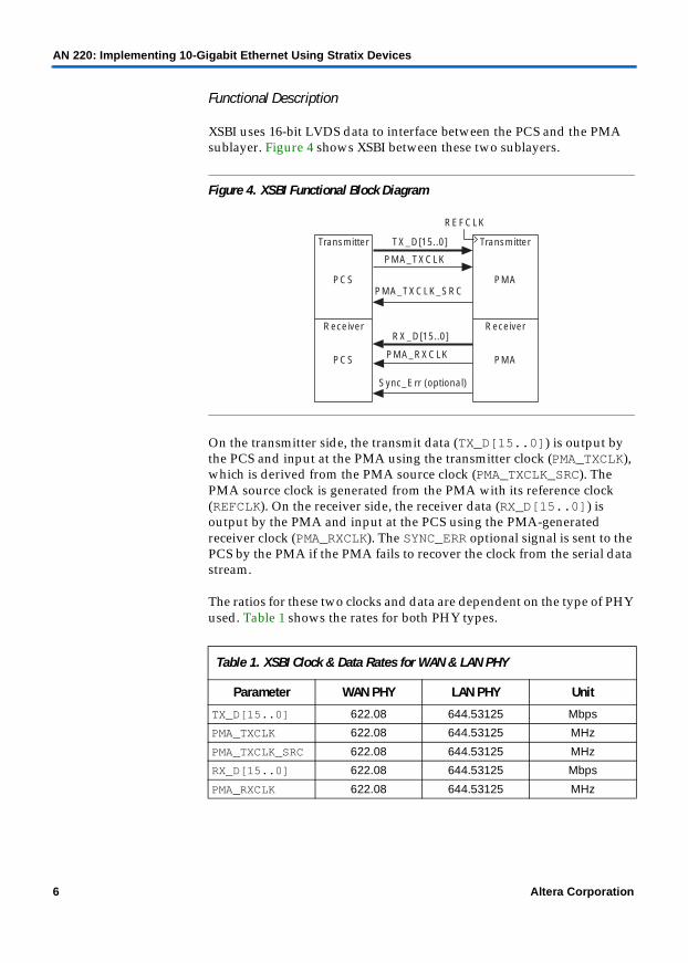
XSBI uses 16-bit LVDS data to interface between the PCS and the PMA sublayer. Figure 4 shows XSBI between these two sublayers.
Figure 4. XSBI Functional Block Diagram
On the transmitter side, the transmit data (TX_D[15..0]) is output by the PCS and input at the PMA using the transmitter clock (PMA_TXCLK), which is derived from the PMA source clock (PMA_TXCLK_SRC). The PMA source clock is generated from the PMA with its reference clock (REFCLK). On the receiver side, the receiver data (RX_D[15..0]) is output by the PMA and input at the PCS using the PMA-generated receiver clock (PMA_RXCLK). The SYNC_ERR optional signal is sent to the PCS by the PMA if the PMA fails to recover the clock from the serial data stream.
The ratios for these two clocks and data are dependent on the type of PHY used. Table 1 shows the rates for both PHY types.
TX_D[15..0]Transmitter
PMA_TXCLK_SRC
RX_D[15..0]
PMA_RXCLK
Sync_Err (optional)
PMA_TXCLK
REFCLK
PCS
PCS
PMA
PMA
Receiver
Transmitter
Receiver
Table 1. XSBI Clock & Data Rates for WAN & LAN PHY
Parameter WAN PHY LAN PHY Unit
TX_D[15..0] 622.08 644.53125 Mbps
PMA_TXCLK 622.08 644.53125 MHz
PMA_TXCLK_SRC 622.08 644.53125 MHz
RX_D[15..0] 622.08 644.53125 Mbps
PMA_RXCLK 622.08 644.53125 MHz
6 Altera Corporation
AN 220: Implementing 10-Gigabit Ethernet Using Stratix Devices
Implementation
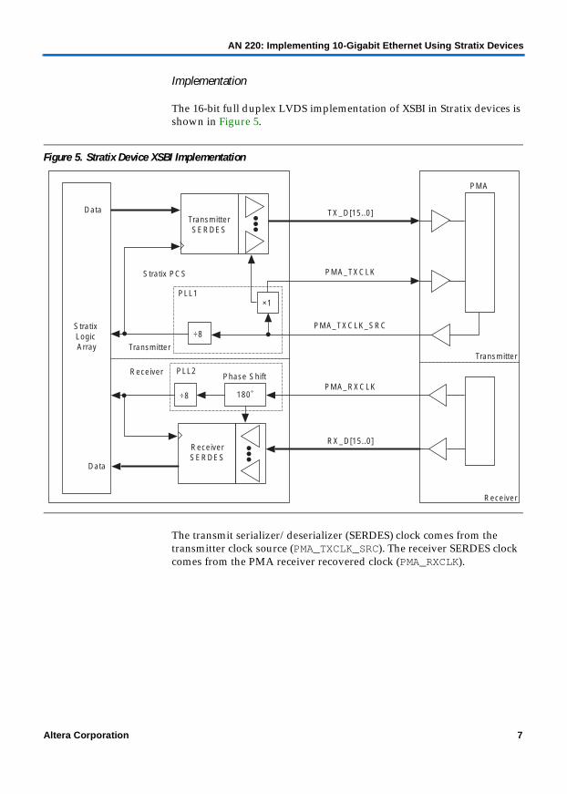
The 16-bit full duplex LVDS implementation of XSBI in Stratix devices is shown in Figure 5.
Figure 5. Stratix Device XSBI Implementation
The transmit serializer/deserializer (SERDES) clock comes from the transmitter clock source (PMA_TXCLK_SRC). The receiver SERDES clock comes from the PMA receiver recovered clock (PMA_RXCLK).
TransmitterSERDES
ReceiverSERDES
×1
÷8
÷8 180˚
Stratix PCS
Data
Data
Transmitter
Receiver
PMA
TX_D[15..0]
PMA_TXCLK
PMA_TXCLK_SRC
PMA_RXCLK
RX_D[15..0]
Phase Shift
Receiver
Transmitter
PLL1
Stratix Logic Array
PLL2
Altera Corporation 7
AN 220: Implementing 10-Gigabit Ethernet Using Stratix Devices
Figure 6 shows the transmitter output of the XSBI core. Data transmitted from the PCS to the PMA starts at the core of the Stratix device and travels to the Stratix transmitter SERDES block. The transmitter SERDES block converts the parallel data to serial data for 16 individual channels (TX_D[15..0]). The PMA source clock (PMA_TXCLK_SRC) is used to clock out the signal data. PMA_TXCLK is generated from the same phase-locked loop (PLL) as the data, and it travels to the PMA at the same rate as the data. By using one of the data channels in the middle of the bus as the clock (in this case, the eighth channel CH8), the clock-to-data skew improves.
Figure 7 shows the receiver input of the XSBI core. From the receiver side, data (RX_D[15..0]) comes from the PMA to the Stratix receiver SERDES block along with the PMA receiver clock (PMA_RXCLK). The PMA receiver clock is used to convert the serial data to parallel data. The phase shift or inversion on the PMA receiver clock is needed to capture the receiver data.
TX_D[0]
Stratix LogicArray
Fast PLL
W = 1J = 4 or 8
4 or 8
Stratix SERDES
× W
CH0
CH16
PMATransmitter
TX_D[15]
PMA_TXCLK_SRC
Stratix PCS Transmitter
÷J
622 MHz
622 MHz
622 Mbps
CH9
CH7
ParallelRegister
Parallel-to-SerialRegister
4 or 8
CH8
TX_D[7]
PMA_TXCLK
TX_D[8]
8 Altera Corporation
AN 220: Implementing 10-Gigabit Ethernet Using Stratix Devices
Stratix devices contain up to eight fast PLLs. These PLLs provide high-speed outputs for high-speed differential I/O support as well as general- purpose clocking with multiplication and phase shifting. The fast PLL incorporates this 180° phase shift. The Stratix device’s data realignment feature enables you to save more logic elements (LEs). This feature provides a byte-alignment capability, which is embedded inside the SERDES. The data realignment circuitry can correct for bit misalignments by slipping data bits.
f For more information about fast PLLs, refer to the Stratix Programmable Logic Device Family Data Sheet.
Figure 7. Stratix XSBI Receiver Implementation
RX_D[0]
Stratix LogicArray
Fast PLL
W = 1J = 4 or 8
4 or 8
Stratix SERDES
× W
CH0
CH15
PMAReceiver
RX_D[15]
PMA_RXCLK_SRC
Stratix PCS Receiver
÷J
622 MHz
622 MHz
622 Mbps
ParallelRegister
Parallel-to-SerialRegister
4 or 8
Altera Corporation 9
AN 220: Implementing 10-Gigabit Ethernet Using Stratix Devices
10 Altera Corporation
With this XSBI transmitter and receiver block implementation, each XSBI core requires two fast PLLs. The potential number of XSBI cores per device corresponds to the number of fast PLLs each Stratix device contains. Table 2 shows the number of LVDS channels, the number of fast PLLs, and the number of XSBI cores that can be supported for each Stratix device.
Notes to Table 2:(1) Preliminary data.(2) The LVDS channels can go up to 840 Mbps.
AC Timing Specifications
Stratix devices support a PCS interface. Figures 8 and 9 and Tables 3 and 4 illustrate timing characteristics of the PCS transmitter and receiver interfaces.
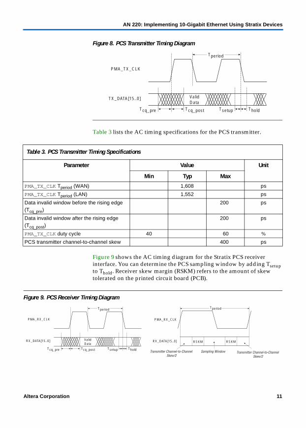
Figure 8 shows the AC timing diagram for the Stratix PCS transmitter. You can determine PCS channel-to-channel skew by adding the data invalid window before the rising edge (Tcq_pre) to the data invalid window after the rising edge (Tcq_post).
Table 2. Stratix Device XSBI Core Support
Stratix Device Number of LVDS Channels
(Receive/Transmit)(1), (2)
Number of Fast PLLs
Number of XSBI Interfaces
(Maximum)
EP1S10 44/44 4 2
EP1S20 66/66 4 2
EP1S25 78/78 4 2
EP1S30 82/82 8 4
EP1S40 90/90 8 4
EP1S60 116/116 8 4
EP1S80 80/40 8 4
EP1S120 80/40 8 4
AN 220: Implementing 10-Gigabit Ethernet Using Stratix Devices
Figure 8. PCS Transmitter Timing Diagram
Table 3 lists the AC timing specifications for the PCS transmitter.
Figure 9 shows the AC timing diagram for the Stratix PCS receiver interface. You can determine the PCS sampling window by adding Tsetup to Thold. Receiver skew margin (RSKM) refers to the amount of skew tolerated on the printed circuit board (PCB).
Figure 9. PCS Receiver Timing Diagram
Tperiod
Tcq_pre Tcq_post Tsetup Thold
ValidData
TX_DATA[15..0]
PMA_TX_CLK
Table 3. PCS Transmitter Timing Specifications
Parameter Value Unit
Min Typ Max
PMA_TX_CLK Tperiod (WAN) 1,608 ps
PMA_TX_CLK Tperiod (LAN) 1,552 ps
Data invalid window before the rising edge (Tcq_pre)
200 ps
Data invalid window after the rising edge (Tcq_post)
200 ps
PMA_TX_CLK duty cycle 40 60 %
PCS transmitter channel-to-channel skew 400 ps
Tperiod
Tcq_pre Tcq_post Tsetup Thold
ValidData
RX_DATA[15..0] RSKM
Sampling Window
RSKM
Transmitter Channel-to-Channel Skew/2
Transmitter Channel-to-Channel Skew/2
Tperiod
RX_DATA[15..0]
PMA_RX_CLK PMA_RX_CLK
Altera Corporation 11
AN 220: Implementing 10-Gigabit Ethernet Using Stratix Devices
Table 4 lists the AC timing specifications for the PCS receiver interface.
XGMII
The purpose of XGMII is to provide a simple, inexpensive, and easy to implement interconnection between the MAC sublayer and the PHY. Though XGMII is an optional interface, it is used extensively in the 10-Gigabit Ethernet standard as the basis for the specification. The conversion between the parallel data paths of XGMII and the serial MAC data stream is carried out by the reconciliation sublayer. The reconciliation sublayer maps the signal set provided at the XGMII to the physical layer signaling (PLS) service primitives provided at the MAC. XGMII supports a 10-Gbps MAC data rate.
Functional Description
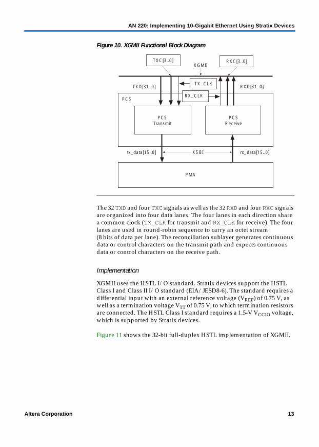
The XGMII is composed of independent transmit and receive paths. Each direction uses 32 data signals, TXD[31..0] and RXD[31..0], 4 control signals, TXC[3..0] and RXC[3..0], and a clock TX_CLK and RX_CLK. Figure 10 shows the XGMII functional block diagram.
Table 4. PCS Receiver Timing Specifications
Parameter Value Unit
Min Typ Max
PMA_RX_CLK Tperiod (WAN) 1,608 ps
PMA_RX_CLK Tperiod (LAN) 1,552 ps
Data invalid window before the rising edge (Tcq_pre)
200 ps
Data invalid window after the rising edge (Tcq_post)
200 ps
PMA_RX_CLK duty cycle 45 55 %
Data set-up time (Tsetup) 300 ps
Data hold time (Thold) 300 ps
PCS sampling window 600 ps
RSKM (WAN) 304 ps
RSKM (LAN) 276 ps
12 Altera Corporation
AN 220: Implementing 10-Gigabit Ethernet Using Stratix Devices
Figure 10. XGMII Functional Block Diagram
The 32 TXD and four TXC signals as well as the 32 RXD and four RXC signals are organized into four data lanes. The four lanes in each direction share a common clock (TX_CLK for transmit and RX_CLK for receive). The four lanes are used in round-robin sequence to carry an octet stream (8 bits of data per lane). The reconciliation sublayer generates continuous data or control characters on the transmit path and expects continuous data or control characters on the receive path.
Implementation
XGMII uses the HSTL I/O standard. Stratix devices support the HSTL Class I and Class II I/O standard (EIA/JESD8-6). The standard requires a differential input with an external reference voltage (VREF) of 0.75 V, as well as a termination voltage VTT of 0.75 V, to which termination resistors are connected. The HSTL Class I standard requires a 1.5-V VCCIO voltage, which is supported by Stratix devices.
Figure 11 shows the 32-bit full-duplex HSTL implementation of XGMII.
PCSTransmit
PCS
PCS Receive
PMA
XGMII
tx_data[15..0] rx_data[15..0]
TXD[31..0] RXD[31..0]
XSBI
TX_CLK
RX_CLK
RXC[3..0]TXC[3..0]
Altera Corporation 13
AN 220: Implementing 10-Gigabit Ethernet Using Stratix Devices
Figure 11. Stratix XGMII Implementation
For this implementation, the shift register clocks can either be generated from a divided down MAC reconciliation sublayer transmitter clock (MAC_TXCLK), or the asynchronous core clock, or both if using a FIFO buffer.
Figure 12 shows one channel of the output half of XGMII. Data that is transmitted from the PCS to the MAC reconciliation sublayer starts at the core of the Stratix device and travels to the shift register. The shift register takes in the parallel data (even bits sent to the top register and odd bits sent to the bottom register) and serializes the data. After the data is serialized, it travels to the double data rate (DDR) output circuitry, which is clocked with the ×4 clock from the PLL. Out of the DDR output circuitry, the data drives off-chip along with the ×4 clock. This transaction creates the DDR relationship between the clock and the data output. This implementation only shows one channel, but can be duplicated to include all 32 bits of the RX_D signal and all 4 bits of the RX_C signal.
ShiftRegister
ShiftRegister
×4
÷4
Clk
Data
Clk
Data
TransmitterReceiver
MAC (RS)
RX_D[31..0]
MAC_RXCLK
MAC_TXCLK
TX_D[31..0]
Receiver
Transmitter
Stratix Logic Array
Stratix PCS
RX_C[3..0]
TX_C[3..0]
DDR Input Circuitry
DDR Output Circuitry
PLL1
PLL2
14 Altera Corporation
AN 220: Implementing 10-Gigabit Ethernet Using Stratix Devices
Figure 13 shows one channel of the input half of the XGMII interface. From the receiver side, the DDR data is captured from the MAC to the Stratix PCS DDR input circuitry. The serial data is separated into two individual data streams with the even bits routed to the top register and odd bits routed to the bottom register. The DDR input circuitry produces two output data streams that go into the shift registers. From the shift registers, the data is deserialized using the clock from the MAC, combining into an 8-bit word. This parallel data goes to a register that is clocked by the divide-by-4 clock from the PLL. This data and clock go to the Stratix core. This implementation shows only one channel, but can be duplicated to include all 32 bits of the TX_D signal and all 4 bits of the TX_C signal.
RX_D[0]
Stratix Logic Array
8
4
MACReceiver
MAC_RXCLK
Stratix PCS Output
156.25 MHz
312.5 Mbps
4
ShiftRegister
D0,D2,D4,D6
D1,D3,D5,D7
DFF
DFF
PLL×4
DATA
CLK
DATA
CLK
39.0625 MHz
156.25 MHz
DDR Output Circuitry
ShiftRegister
Altera Corporation 15
AN 220: Implementing 10-Gigabit Ethernet Using Stratix Devices
Stratix devices contain up to four enhanced PLLs. These PLLs provide features such as clock switchover, spread-spectrum clocking, programmable bandwidth, phase and delay control, and PLL reconfiguration. Since the maximum clock rate is 156.25 MHz, you can use a fast or enhanced PLL for both the XGMII output and input blocks.
f For more information about fast PLLs, refer to the Stratix Programmable Logic Device Family Data Sheet.
TX_D[0]
8 8
MAC_TXCLK
Stratix PCS Input
156.25 MHz
312.5 Mbps
4
ShiftRegister
DDR Input Circuitry
D0,D2,D4,D6
D1,D3,D5,D7
39.0625 MHz
156.25 MHz
MAC Transmitter
DATA
CLK
Stratix LogicArray
DATA
CLK
DFF
DFF Latch
DFF
PLL
4
ShiftRegister
÷4
16 Altera Corporation
AN 220: Implementing 10-Gigabit Ethernet Using Stratix Devices
Altera Corporation 17
With this implementation for the XGMII output and input blocks, the number of XGMII cores per device corresponds to the number of PLLs each Stratix device contains. Table 5 shows the number of HSTL I/O pins, PLLs, and XGMII cores that are supported in each Stratix device. Each core requires 72 HSTL I/O pins for data and control and 2 clock pins for the transmitter and receiver clocks. Each XGMII core also needs two PLLs (one for each direction).
Reduced System Noise
The output buffer of each Stratix device I/O pin has a programmable drive strength control for certain I/O standards. The HSTL Class I standard supports the minimum setting, which is the lowest drive strength that guarantees IOH and IOL of the standard. Using minimum settings provides signal slew rate control to reduce system noise and signal overshoot.
f For more information on IOH and IOL values, refer to the Operating Conditions section of the Stratix Programmable Logic Device Family Data Sheet
Table 5. Stratix XGMII Core Support
Stratix Device Number of HSTL Class I I/O Pins
Number of Fast & Enhanced
PLLs
Number of XGMII Interfaces
EP1S10 410 6 3
EP1S20 570 6 3
EP1S25 690 6 3
EP1S30 718 10 5
EP1S40 814 12 6
EP1S60 1,014 12 6
EP1S80 1,195 12 6
EP1S120 1,195 12 6
AN 220: Implementing 10-Gigabit Ethernet Using Stratix Devices
On-Chip Termination Support
Stratix devices provide a TerminatorTM technology capability for on-chip parallel termination support for HSTL (Class I and II). Terminator technology can be used at the drivers and receivers to avoid implementing an external pull-up termination resistor. Table 6 describes the values of on-chip termination used by the HSTL I/O standard. Terminator technology supports only one type of on-chip termination I/O standard per given I/O bank.
Figure 14 describes the circuit topology for HSTL.
Figure 14. HSTL Circuit Topology
Timing
XGMII signals must meet the timing requirements shown in Figure 15. Make all XGMII timing measurements at the driver output with the optional termination (shown in Figure 14) and a capacitive load from all sources of 20 pF that are specified relative to the VIL_AC(max) and VIH_AC(min) thresholds.
Table 6. HSTL Class I Termination
I/O Standard On-Chip Termination
RTo RTi VCCN
HSTL Class I HSTL_I_OCT - 50 Ω 1.5 V
Z0
Driving Device with on-chip Parallel Termination
Receiver Device with On-Chip Parallel Termination
VREF
R Ti
VTTVCCN
R To
VCCN
VSSN
18 Altera Corporation
AN 220: Implementing 10-Gigabit Ethernet Using Stratix Devices
Figure 15. XGMII Timing Diagram
Table 7 shows the XGMII timing specifications.
Note to Table 7(1) The actual set-up and hold times will be made available after device
characterization is complete.
Stratix devices support DDR data with clock rates of up to 200 MHz, well above the XGMII clock rate of 156.25 MHz. For the HSTL Class I I/O standard, Stratix device I/O drivers provide a 1.0-V/ns slew rate at the input buffer of the receiving device.
XAUI
XAUI (pronounced Zowie) is located between the XGMII at the reconciliation sublayer and the XGMII at the PHY layer. Figure 16 shows the location of XAUI. XAUI is designed to either extend or replace XGMII in chip-to-chip applications of most Ethernet MAC to PHY interconnects.
tsetupthold
tsetupthold
TX_CLK
RX_CLK
TXC, TXD,RXC, RXD
VIH_AC(min)
VIL_AC(max)
VIH_AC(min)
VIL_AC(max)
Table 7. XGMII Timing Specifications Note (1)
Symbol Driver Receiver Unit
Tsetup 960 480 ps
Thold 960 480 ps
Altera Corporation 19
AN 220: Implementing 10-Gigabit Ethernet Using Stratix Devices
Figure 16. XAUI Location
Functional Description
XAUI can replace the 32 bits of parallel data required by XGMII for transmission with just 4 lanes of serial data. XAUI uses clock data recovery (CDR) to eliminate the need for separate clock signals. 8b/10b encoding is employed on the data stream to embed the clock in the data. The 8b/10b protocol to encode an 8-bit word stream to 10-bit codes that results in a DC-balanced serial stream and eases the receiver synchronization. To support 10-Gigabit Ethernet, each lane must run at a speed of at least 2.5 Gbps. Using 8b/10b encoding increases the rate for each lane to 3.125 Gbps, which will be supported in next-generation Stratix devices. Figure 17 shows how XAUI will be implemented.
XGXS
PHY
XAUI
XGMII
XGMII
Reconciliation
MAC
XGMII ExtenderSublayer (XGXS)
20 Altera Corporation
AN 220: Implementing 10-Gigabit Ethernet Using Stratix Devices
The three interfaces of 10-Gigabit Ethernet (XSBI, XGMII, and XAUI) each have different rates and I/O standards. Table 8 shows the characteristics for each interface.
AN 220: Implementing 10-Gigabit Ethernet Using Stratix Devices
Software Implementation
You can use the Assignment Organizer in the Altera® Quartus® II software to implement the I/O standards for a particular interface. For example, set the I/O standard to LVDS for XSBI and to HSTL Class I for XGMII. You can use the MegaWizard® Plug-In Manager to create the PLLs and transmitter and receiver SERDES blocks for the XSBI implementation and PLLs and DDR input and output circuitry for the XGMII implementation. For more information on the Assignment Organizer or MegaWizard Plug-In Manager, refer to Quartus II Help.
AC/DC Specifications
Table 9 lists the XSBI DC electrical characteristics, similar to Stratix devices, that are based on the ANSI/TIA-644 LVDS specification.
Note to Table 9:(1) Larger VOD is possible for better signal intensity.
I/O characteristics for the HSTL standard for Stratix devices are shown in Figure 18 and comply with XGMII electrical specifications available in 10-Gigabit Ethernet draft IEEE P802.3ae.
Table 9. XSBI DC Specifications
Parameter Value Unit
Min Typ Max
Output differential voltage (VOD) 250 400 (1) mV
Output offset voltage (VOS) 1,125 1,375 mV
Output Impedance, single ended 40 140 ΩChange in VOD between ‘0’ and ‘1’ 50 mV
Change in VOS between ‘0’ and ‘1’ 50 mV
Input voltage range (VI) 900 1,600 mV
Differential impedance 100 ΩInput differential voltage (VID) 100 600 mV
AN 220: Implementing 10-Gigabit Ethernet Using Stratix Devices
Figure 18. Electrical Characteristics for Stratix Devices (1.5-V HSTL Class I)
Table 10 lists the DC specifications for Stratix devices (1.5-V HSTL Class I).
Note to Table 10:(1) Drive strength is programmable according to values shown in the Stratix Programmable Logic Device Family Data
Sheet.
VREFCL = 20pF
VINVOUT
RT = 50 Ω
VTT
Output BufferInput Buffer
tz(min) = 1 V/ns
tPD
HSTL AC Load Circuit for Class I
HSTL AC Waveform & I/O Interface
tf(min) = 1 V/ns
VSWING = 1.0 V
Input
Output
Tri-StatedOutput
tPL2
tPH2
80% VSWING
VREF
20% VSWING
VOH = VCCN − 0.4 V = 1.1 V
VTT = VCCN/2 = 0.75 V
VOL = 0.4 V
VIH(AC) = 0.95 V
VTT = 0.75 V
VIL(AC) = 0.55 V
Table 10. DC Specifications for Stratix Devices (1.5-V HSTL Class I) Note (1)
Symbol Parameter Conditions Minimum Typical Maximum Units
VCCIO I/O supply voltage 1.4 1.5 1.6 V
VREF Input reference voltage 0.68 0.75 0.9 V
VTT Termination voltage 0.7 0.75 0.8 V
VIH (DC) DC high-level input voltage VREF + 0.1 V
VIL (DC) DC low-level input voltage –0.3 VREF – 0.1 V
VIH (AC) AC high-level input voltage VREF + 0.2 V
VIL (AC) AC low-level input voltage VREF – 0.2 V
II Input pin leakage current 0 < VIN < VCCIO –10 10 µA
VOH High-level output voltage IOH = –8 mA VCCIO – 0.4 V
VOL Low-level output voltage IOL = 8 mA 0.4 V
IO Output leakage current (when output is high Z)
GND ≤ VOUT ≤ VCCIO
–10 10 µA
Altera Corporation 23
AN 220: Implementing 10-Gigabit Ethernet Using Stratix Devices
10-Gigabit Ethernet MAC Core
As an Altera Megafunction Partners Program (AMPPSM) member, MorethanIP provides a 10-Gigabit Ethernet MAC core for Altera customers. MorethanIP’s 10-Gigabit Ethernet MAC core implements the RS, the MAC layer, and user-programmable FIFO buffers for clock and data decoupling.
Core Features
MorethanIP’s 10-Gigabit Ethernet MAC core provides the following features:
Includes automatic pause frame generation (per IEEE 802.3 ×31) with user-programmable pause quanta and pause-frame termination
Includes a programmable 48-bit MAC address with a promiscuous mode option, and a programmable Ethernet frame length that supports IEEE 802.1Q VLAN-tagged frames or jumbo Ethernet frames
Supports broadcast traffic and multi-cast address resolution with a 64-entry hash table
Compliant with the IEEE802.3ae Draft 4.0 Implements XGMII, allowing it to interface to XAUI through a
10-Gigabit commercial SERDES
Conclusion
10-Gigabit Ethernet takes advantage of the existing Gigabit Ethernet standard. With its rich I/O features, Stratix devices supports the components of 10-Gigabit Ethernet as well as XSBI and XGMII. With the next-generation of Stratix devices, XAUI will also be supported. These interfaces are easily implemented using Stratix’s core architecture, differential I/O capabilities, and superior PLLs.