Altera Corporation 1 AN-448-1.3 Application Note 448 Stratix III Power Management Design Guide Introduction This document provides recommendations and guidelines for power management system design in systems featuring Altera Stratix ® III FPGAs. To help you design a proper power solution for your system, this document focuses on the areas and design flow shown in Figure 1. Figure 1. Power Management Design Flow There are many application-specific aspects to consider when powering digital ICs, such as DC tolerance, system sequencing, and transient requirements. In addition, other concerns such as system cost, PCB real estate, and efficiency play a crucial role in defining the final power solution. This design example sequences through the design flow, as shown in Figure 1. For this design example, an analog to digital converter (ADC) and Memory IC will be integrated with a Stratix III device, as shown in Figure 2. Note that this is not a reference design and the final solution only exhibits one of the many possible power solutions for the application. Cost, Size, and Efficiency Tradeoffs Determining Power Management Specifications for Selected ICs Choosing a Power Distribution Architecture Creating a Power Budget Spreadsheet Complying with Thermal and Signal Integrity Requirements Defining PCB Layout and Voltage Regulator Selection May 2007, Version 1.3
Transcript
Altera Corporation AN-448-1.3
May 2007, Version 1.3
Stratix III Power ManagementDesign Guide
Application Note 448
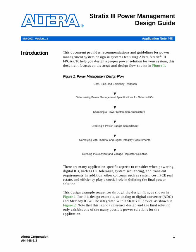
Introduction This document provides recommendations and guidelines for power management system design in systems featuring Altera Stratix® III FPGAs. To help you design a proper power solution for your system, this document focuses on the areas and design flow shown in Figure 1.
Figure 1. Power Management Design Flow
There are many application-specific aspects to consider when powering digital ICs, such as DC tolerance, system sequencing, and transient requirements. In addition, other concerns such as system cost, PCB real estate, and efficiency play a crucial role in defining the final power solution.
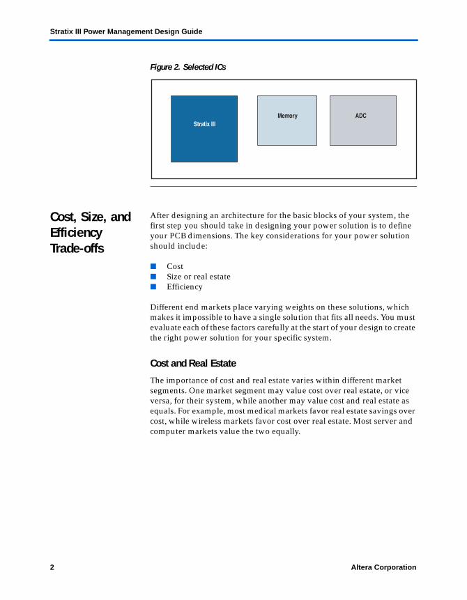
This design example sequences through the design flow, as shown in Figure 1. For this design example, an analog to digital converter (ADC) and Memory IC will be integrated with a Stratix III device, as shown in Figure 2. Note that this is not a reference design and the final solution only exhibits one of the many possible power solutions for the application.
Cost, Size, and Efficiency Tradeoffs
Determining Power Management Specifications for Selected ICs
Choosing a Power Distribution Architecture
Creating a Power Budget Spreadsheet
Complying with Thermal and Signal Integrity Requirements
Defining PCB Layout and Voltage Regulator Selection
1
Stratix III Power Management Design Guide
Figure 2. Selected ICs
Cost, Size, and Efficiency Trade-offs
After designing an architecture for the basic blocks of your system, the first step you should take in designing your power solution is to define your PCB dimensions. The key considerations for your power solution should include:
■ Cost■ Size or real estate ■ Efficiency
Different end markets place varying weights on these solutions, which makes it impossible to have a single solution that fits all needs. You must evaluate each of these factors carefully at the start of your design to create the right power solution for your specific system.
Cost and Real Estate
The importance of cost and real estate varies within different market segments. One market segment may value cost over real estate, or vice versa, for their system, while another may value cost and real estate as equals. For example, most medical markets favor real estate savings over cost, while wireless markets favor cost over real estate. Most server and computer markets value the two equally.
Stratix III Memory ADC
2 Altera Corporation
Cost, Size, and Efficiency Trade-offs
Efficiency
Efficiency of your power solution is primarily dependent on the voltage regulator, and is defined as the output power divided by the input power. Systems such as cellular base stations, servers, and any system that requires batteries are typically very concerned about efficiency. If efficiency is critical to your system, you should take into account the following considerations:
■ Type of cooling system on the application. The better the cooling system, the more efficient it is.
■ Amount of wattage available as power budget for the board. The lower the efficiency, the more power is dissipated by the voltage regulator circuitry.
The type of efficiency requirement needed dictates the type of voltage regulator circuitry to use. There are two different voltage regulators available on the market:
■ Switching regulators
This type of regulator has a higher efficiency, generally above 90%. However, efficiency drops sharply with higher temperatures, the rate of which depends on the manufacturer.
■ Linear regulators
The efficiency of linear regulators is Vout/Vin. For example, if Vout is 1.5 V and Vin is 3.3 V, efficiency is very low, and equals 45.5%.
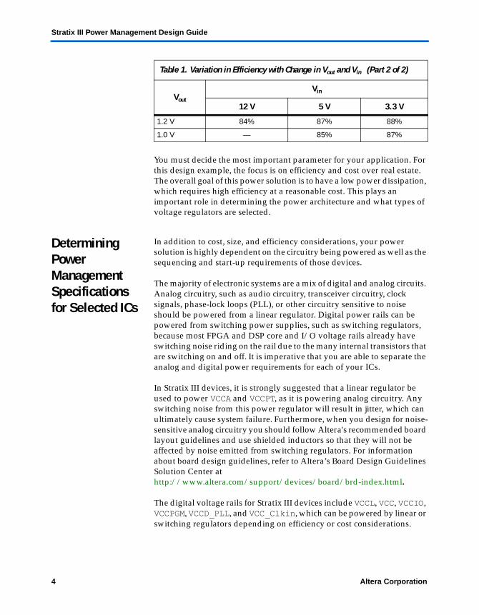
Refer to Table 1 for variation in efficiency with change in Vout and V.
Table 1. Variation in Efficiency with Change in Vout and Vin (Part 1 of 2)
Vout
Vin
12 V 5 V 3.3 V
5 V 93% — —
3.3 V 91% 95% —
2.5 V 89% 93% 94%
2.3 V 88% 91% 92%
1.8 V 87% 90% 91%
1.5 V 86% 89% 90%
Altera Corporation 3
Stratix III Power Management Design Guide
You must decide the most important parameter for your application. For this design example, the focus is on efficiency and cost over real estate. The overall goal of this power solution is to have a low power dissipation, which requires high efficiency at a reasonable cost. This plays an important role in determining the power architecture and what types of voltage regulators are selected.
Determining Power Management Specifications for Selected ICs
In addition to cost, size, and efficiency considerations, your power solution is highly dependent on the circuitry being powered as well as the sequencing and start-up requirements of those devices.
The majority of electronic systems are a mix of digital and analog circuits. Analog circuitry, such as audio circuitry, transceiver circuitry, clock signals, phase-lock loops (PLL), or other circuitry sensitive to noise should be powered from a linear regulator. Digital power rails can be powered from switching power supplies, such as switching regulators, because most FPGA and DSP core and I/O voltage rails already have switching noise riding on the rail due to the many internal transistors that are switching on and off. It is imperative that you are able to separate the analog and digital power requirements for each of your ICs.
In Stratix III devices, it is strongly suggested that a linear regulator be used to power VCCA and VCCPT, as it is powering analog circuitry. Any switching noise from this power regulator will result in jitter, which can ultimately cause system failure. Furthermore, when you design for noise-sensitive analog circuitry you should follow Altera's recommended board layout guidelines and use shielded inductors so that they will not be affected by noise emitted from switching regulators. For information about board design guidelines, refer to Altera’s Board Design Guidelines Solution Center at http://www.altera.com/support/devices/board/brd-index.html.
The digital voltage rails for Stratix III devices include VCCL, VCC, VCCIO, VCCPGM, VCCD_PLL, and VCC_Clkin, which can be powered by linear or switching regulators depending on efficiency or cost considerations.
1.2 V 84% 87% 88%
1.0 V — 85% 87%
Table 1. Variation in Efficiency with Change in Vout and Vin (Part 2 of 2)
Determining Power Management Specifications for Selected ICs
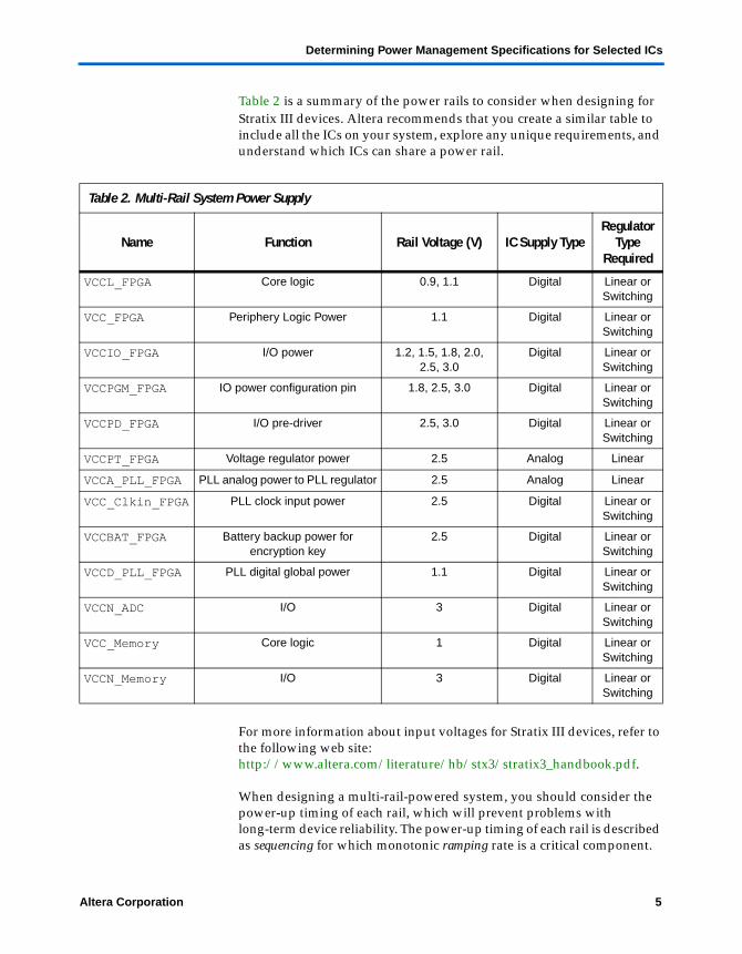
Table 2 is a summary of the power rails to consider when designing for Stratix III devices. Altera recommends that you create a similar table to include all the ICs on your system, explore any unique requirements, and understand which ICs can share a power rail.
For more information about input voltages for Stratix III devices, refer to the following web site: http://www.altera.com/literature/hb/stx3/stratix3_handbook.pdf.
When designing a multi-rail-powered system, you should consider the power-up timing of each rail, which will prevent problems with long-term device reliability. The power-up timing of each rail is described as sequencing for which monotonic ramping rate is a critical component.
Table 2. Multi-Rail System Power Supply
Name Function Rail Voltage (V) IC Supply TypeRegulator
Type Required
VCCL_FPGA Core logic 0.9, 1.1 Digital Linear or Switching
VCC_FPGA Periphery Logic Power 1.1 Digital Linear or Switching
VCCIO_FPGA I/O power 1.2, 1.5, 1.8, 2.0, 2.5, 3.0
Digital Linear or Switching
VCCPGM_FPGA IO power configuration pin 1.8, 2.5, 3.0 Digital Linear or Switching
VCCPD_FPGA I/O pre-driver 2.5, 3.0 Digital Linear or Switching
VCCPT_FPGA Voltage regulator power 2.5 Analog Linear
VCCA_PLL_FPGA PLL analog power to PLL regulator 2.5 Analog Linear
VCC_Clkin_FPGA PLL clock input power 2.5 Digital Linear or Switching
VCCBAT_FPGA Battery backup power for encryption key
2.5 Digital Linear or Switching
VCCD_PLL_FPGA PLL digital global power 1.1 Digital Linear or Switching
VCCN_ADC I/O 3 Digital Linear or Switching
VCC_Memory Core logic 1 Digital Linear or Switching
There are three methods for controlling power-up sequencing:
■ Simultaneous■ Ratio-metric■ Sequential
Figure 3 shows an example where all rails ramp simultaneously and stop at their intended regulation point. The rails also rise at the same rate, which prevents latch-up, bus contention, and undesirable transistor states. As such, simultaneous sequencing is considered to be the ideal sequencing method. The drawback, however, is that simultaneous sequencing may require more system start-up currents because all power rails across the system ramp up simultaneously. Special circuits, such as voltage regulators (VR) with simultaneous sequencing options, are required for implementation.
Figure 3. Simultaneous Sequencing
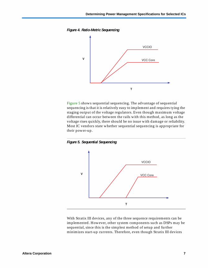
Figure 4 shows an example of ratio-metric sequencing. With this sequencing, the rails rise at different ramp rates, but the higher voltage rail has a faster slew rate, making each arrive at their regulation point at the same time. The advantage to this sequencing is that it keeps the voltage differential between power rails to a minimum. The disadvantage of this sequencing is that it may also require more system start-up currents since all power rails start up at the same time. This type of sequencing requires a voltage regulator with a controllable soft-start option.
VCCIO
VCC CoreV
T
6 Altera Corporation
Determining Power Management Specifications for Selected ICs
Figure 4. Ratio-Metric Sequencing
Figure 5 shows sequential sequencing. The advantage of sequential sequencing is that it is relatively easy to implement and requires tying the staging output of the voltage regulators. Even though maximum voltage differential can occur between the rails with this method, as long as the voltage rises quickly, there should be no issue with damage or reliability. Most IC vendors state whether sequential sequencing is appropriate for their power-up.
Figure 5. Sequential Sequencing
With Stratix III devices, any of the three sequence requirements can be implemented. However, other system components such as DSPs may be sequential, since this is the simplest method of setup and further minimizes start-up currents. Therefore, even though Stratix III devices
VCCIO
VCC CoreV
T
VCCIO
VCC CoreV
T
Altera Corporation 7
Stratix III Power Management Design Guide
are very tolerant to your input power sequencing, it is critical that you check other components in your system to understand their sequencing requirements.
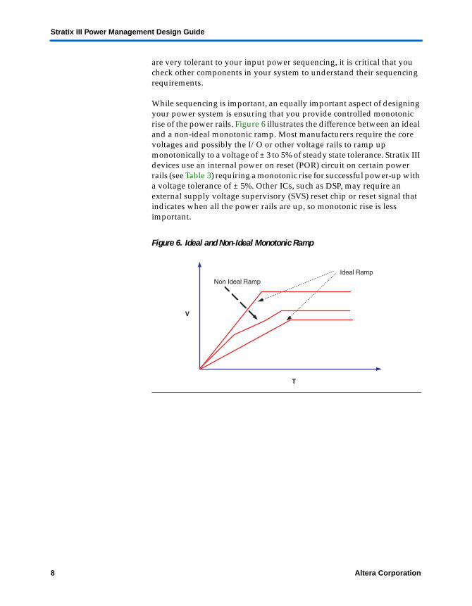
While sequencing is important, an equally important aspect of designing your power system is ensuring that you provide controlled monotonic rise of the power rails. Figure 6 illustrates the difference between an ideal and a non-ideal monotonic ramp. Most manufacturers require the core voltages and possibly the I/O or other voltage rails to ramp up monotonically to a voltage of ± 3 to 5% of steady state tolerance. Stratix III devices use an internal power on reset (POR) circuit on certain power rails (see Table 3) requiring a monotonic rise for successful power-up with a voltage tolerance of ± 5%. Other ICs, such as DSP, may require an external supply voltage supervisory (SVS) reset chip or reset signal that indicates when all the power rails are up, so monotonic rise is less important.
Figure 6. Ideal and Non-Ideal Monotonic Ramp
Ideal RampNon Ideal Ramp
V
T
8 Altera Corporation
Determining Power Management Specifications for Selected ICs
The Stratix III power supplies shown in Table 3 are monitored by POR circuitry and need to reach the stated voltage levels to ensure that all the circuits in the FPGA are at known states during power-up.
Stratix III ramp rate requirements for the power supplies listed in Table 3 are:
■ MAX ramp rate = 100 mS■ MIN ramp rate = 50 µS■ All supplies must be strictly monotonic—without plateaus
For more information about Stratix III ramp rate requirements and POR monitored power supplies, refer to the following web site:http://www.altera.com/literature/hb/stx3/stratix3_handbook.pdf.
Even when minimum ramp time requirements are met, the voltage regulators need to be soft started. A soft-start function minimizes input current by gradually increasing the current limit at startup, slowing the rate of rise of the output voltage, and reducing the peak current required when starting up. This prevents the sudden rush of current needed for charging bulk capacitance from exceeding the current limit of the voltage regulator, which could cause it to start up improperly to prevent damage from overcurrent.
For this design example, a sequential sequencing with soft-start is used, since it is the easiest one to implement and is a reliable power-up strategy. This method is especially useful when the power supply capabilities of the system are either unknown or are being burdened by other components in a system. By tying the staging output of the voltage regulators, you can enable subsequent voltage regulators and create a sequential power-up scheme. The SVS on the input rail prevents the voltage regulator from turning on until the input capacitors are charged and the rail is up, which reduces the chances of tripping the undervoltage lockout (UVLO) of the voltage regulator. This power management system, shown in Figure 7, addresses the power-up requirements and start-up issues.
Figure 7. Power Management System for Sequential Sequencing
Choosing a Power Distribution Architecture
The architecture of your overall power solution is defined by many of the factors previously discussed, including input voltage of the system, tolerance, dynamic response, system efficiency, and PCB real estate. Determining the relative priority of these system characteristics determines the optimum power distribution architecture for your particular application. In general, there are two basic approaches to power distribution. One is a single-source conversion system, and the other is intermediate bus architecture (IBA) conversion, which uses point of load (POL) voltage regulators. Both are summarized below:
Single-Source
■ Distributed power architecture (DPA)
Intermediate Bus Architecture
■ Regulated intermediate bus architecture ■ Unregulated intermediate bus architecture
Stratix III
ADC
Memory
EN
EN
EN
Vin
Vin
Vin
UVLO /SVS
Vout
Vout
Vout
DC/DC Voltage Regulator
DC/DC Voltage Regulator
DC/DC Voltage Regulator
10 Altera Corporation
Choosing a Power Distribution Architecture
In many multi-rail applications, using intermediate bus architecture brings considerable financial savings as well as performance benefits. Current requirements can vary widely across different applications. For example, typical server systems require up to 90 amps, while portable medical systems typically require 1 amp. Your particular power architecture solution will be unique, since your application has different requirements.
Distributed Power Architecture
DPA implies a collection of two or more isolated DC/DC converters, or isolated bricks, each supplying one to three output voltages and operating from a common intermediate bus voltage. DPA is common in telecom networking systems, which are usually 48 V. In the DPA, the power converters are located in close physical proximity to the load circuitry, minimizing DC distribution losses and reducing distribution inductance for enhanced dynamic response performance. However, in many applications when no isolation is required, or very low voltages are needed, this type of system has limitations and can be costly. Figure 8 illustrates a basic block of DPA.
Figure 8. DPA Basic Block
Vin (volts) IsolatedBrick
IsolatedBrick
IsolatedBrick
Vout (Volts) @ Iout (amps)
Altera Corporation 11
Stratix III Power Management Design Guide
Advantages:
■ Single level of power conversion provides improved overall efficiency.
■ Higher power systems benefit from lower current in distribution bus.
■ Works well in systems requiring few voltage rails.
Disadvantages:
■ Reduced transient response handling compared to POL voltage regulators.
■ Additional bypass capacitors may be required.■ Higher system cost due to multiple isolation barriers; as voltage rails
increase, cost and PC board space increases.■ No sequencing without external circuitry.
Intermediate Bus Architecture (IBA)
The intermediate bus architecture is classified into two categories: unregulated bus converters and regulated bus converters. The two categories are discussed in the following sections, and a comparison is shown in Table 4. The advantages and disadvantages of the IBA architecture are listed below, which will vary depending on the type of IBA architecture used.
Advantages:
■ Improved transient response provided by POL voltage regulators.■ Lower cost is achieved due to single isolation barrier.■ Minimized PCB board space.
Disadvantages:
■ A two-step conversion process results in increased power loss and higher input requirement.
■ High currents in distribution bus may be unmanageable in higher power systems.
Unregulated Intermediate Bus Architecture
The unregulated bus system employs an isolated but unregulated intermediate bus converter (IBC) function to drop the input voltage to a nominal level for usage by the POL voltage regulators. This voltage reduction is desirable because POL voltage regulators operate most efficiently between the input and output voltages, so the duty cycle of the
12 Altera Corporation
Choosing a Power Distribution Architecture
buck voltage regulator is optimized. Systems with high total output power tend to favor the unregulated IBA, especially if high currents or power levels are present on two or more output voltages.
The following are characteristics of unregulated IBA:
■ Limited input range of 36 to 75 V.■ Board space consumption minimized.■ Provides for optimum conversion efficiency for POL
voltage regulators.■ Provides highest system efficiency for high power systems.■ Allows for sequencing of all voltage rails.
The basic block of unregulated IBA is illustrated in Figure 9.
Figure 9. Unregulated IBA
Regulated Voltage Intermediate Bus Architecture
The regulated bus approach works best when the output voltage with the highest current is at a voltage level commonly used as an input for POL voltage regulators, such as 5 V or 3.3 V. If the maximum output power is required at a voltage of 2.5 V or lower, the regulated bus architecture is not a good choice. The regulated bus approach is often the best choice for lower power systems with most of the output power concentrated on one output voltage.
POL
POL
POL
3.3V@6A
2.5V@4A
Voltage@Current
Quasi-IsolatedBrick
36 to 75 V
Altera Corporation 13
Stratix III Power Management Design Guide
The following are characteristics of regulated IBA:
■ Uses one isolated brick and many non-isolated POLs.■ Uses a regulated 3.3-V, 5-V, or 12-V bus for the POL voltage regulator
input.■ Results in lower cost, less board space, but less efficiency in high
power systems.■ Requires higher bus voltage for POLs, reducing conversion
efficiency (12-V input).■ System cost lower for low power system.
The basic block of regulated IBA is illustrated in Figure 10.
Figure 10. Regulated IBA
A comparison of regulated IBA and unregulated IBA is shown in Table 4.
POL
POL
POL
3.3V@6A
2.5V@4A
Voltage@Current
IsolatedBrick48V
Table 4. Comparison of Regulated IBA and Unregulated IBA (Part 1 of 2)
Parameters Regulated IBA Unregulated IBA
Low Power System Lower cost Higher cost
High Power System Higher cost Lower cost
Low Power System Equal efficiency Equal efficiency
High Power System Lower efficiency Higher efficiency
14 Altera Corporation
Creating a Power Budget Spreadsheet
Creating a Power Budget Spreadsheet
After you have reviewed the type of circuitry being powered, including critical power system requirements such as sequencing recommendations and power architecture solutions, a power budget spreadsheet can be formed. The power budget spreadsheet has become a very important part of the design process due to the size and power requirements of components in your system. In typical applications, listed from most to least, the PCB components that take up most of the power are: CPU, DSP, FPGAs, ASSPs, and ADCs. Most IC manufacturers provide online power-consumption estimators that provide at least a working estimate of the maximum dynamic current. Altera offers the Early Power Estimator and Quartus® II PowerPlay analyzer to help you determine your maximum current draw for any Stratix III design. Once the current consumption for each rail is known, a system power budget spreadsheet can be used to determine the best approach to formulating power architecture. Table 5 summarizes the system voltage rail current requirements and enables the grouping of rails with the same voltage and sequencing for the design.
1 Note that the current values used in Table 5 are estimates based on a test design and not device specifications.
Input Voltage Range Full Telecom, Datacom Restricted Telecom, Datacom
Table 4. Comparison of Regulated IBA and Unregulated IBA (Part 2 of 2)
Parameters Regulated IBA Unregulated IBA
Table 5. Example Design Voltage Rail Summary (Part 1 of 2)
Name Function Rail Voltage (V) Total Worst Case Current Converter
VCCL_FPGA Core logic 1.16 A 8 AVCC_FPGA Periphery logic power 1.1
VCC_ADC Core logic 1.1
VCCIO_FPGA I/O power 2.5 2 3
Altera Corporation 15
Stratix III Power Management Design Guide
ed
Table 6 shows the voltage and current requirements for this design example to attain the targeted system efficiency and power dissipation numbers at point of load. This can be done by selecting converters with different efficiencies, trying different bus voltages, or using converter staging to improve efficiency, as shown in Figure 11. Note that system cost, PCB real estate, and efficiency are additional factors to consider when compiling the power budget, ultimately influencing converter selection. The resulting power calculation plays an important part in thermal compliance and in ensuring that the system’s thermal budget can be handled by your cooling solution.
VCCPGM_FPGA I/O power configuration pin 3.01.5 2VCCPD_FPGA I/O pre-driver 3.0
VCCPT_FPGA Voltage regulator power 2.5
VCCA_PLL_FPGA PLL analog power to PLL regulator 2.50.5 1VCC_Clkin_FPGA PLL clock input power 2.5
VCCBAT_FPGA Battery backup power for encryption key
2.5
VCCD_PLL_FPGA PLL digital global power 1.1 0.3 0.5
VCCN_ADC I/O 3 1.6 2
VCC_Memory Core logic 1 0.8 1
VCCN_Memory I/O 3 0.4 0.5
Total — 14 — 8
Table 5. Example Design Voltage Rail Summary (Part 2 of 2)
Name Function Rail Voltage (V) Total Worst Case Current Converter
Table 6. Budget Calculations (Part 1 of 2)
Converter POL Vout (V)
Approx I out (A)
P out (W)
POL Converter Input (V)
Est Efficiency
P in = Pout/Efficiency
In Required = Pin/Vin (A)
PowerDissipat
VR #1 Switching 1.1 8 8.8 5 0.9 9.77 1.95 0.97
VR #6 Switching 1.8 2 3.6 5 0.89 4.04 0.80 0.44
VR #2 Switching 2.5 3 7.5 5 0.92 8.15 1.63 0.65
VR #3 Linear 3 2 6 5 0.6 10 2 4
VR #4 Linear 2.5 1 2.5 5 0.6 4.16 0.83 2.08
VR #5 Linear 1 0.5 0.5 5 0.4 1.25 0.25 1
VR #7 Linear 1 1 1 5 0.4 2.5 0.5 2
16 Altera Corporation
Creating a Power Budget Spreadsheet
ed
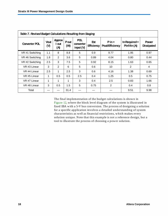
This design uses switching voltage regulators for POL voltage regulators (VR) 1, 2, and 6 to supply the large current demands of our digital circuitry for the Stratix III and ADC devices. The switching regulators also provide higher efficiency and reduced power dissipation. The remaining converters are linear to demonstrate the effect of staging converters to improve system power dissipation. By choosing different bus voltages (3.3, 5, 12 V) for the IBA architecture, optimized converter efficiency can be at the cost of current. As bus voltage is lowered, the bus current increases and creates a trade-off between efficiency and current density. Staging can be applied to the linear regulators to minimize power dissipation and improve efficiency without changing POL bus voltage by narrowing the input to output voltage differential for these linear voltage regulators. Table 7 shows the resulting power dissipation when staging is used to improve the efficiency of VR 4, 5, and 7. Design techniques, such as staging shown in Figure 11, can be very valuable when trying to optimize power dissipation within power architecture.
Figure 11. Using Staging to Improve Efficiency
VR #8 Linear 3 0.5 1.5 5 0.75 2 0.4 0.8
Total — — 31.4 — — — 8.37 11.95
Table 6. Budget Calculations (Part 2 of 2)
Converter POL Vout (V)
Approx I out (A)
P out (W)
POL Converter Input (V)
Est Efficiency
P in = Pout/Efficiency
In Required = Pin/Vin (A)
PowerDissipat
POL
POL
Vout to first device
Vout to trigger second POL
Vout to second device
Altera Corporation 17
Stratix III Power Management Design Guide
d
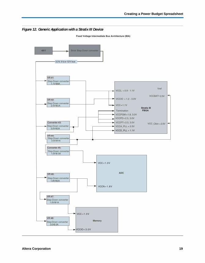
The final implementation of the budget calculations is shown in Figure 12, where the block level diagram of the system is illustrated in fixed IBA with a 5-V bus conversion. The process of designing a solution for a specific application involves a detailed understanding of system characteristics as well as financial restrictions, which makes every solution unique. Note that this example is not a reference design, but a tool to illustrate the process of choosing a power solution.
Table 7. Revised Budget Calculations Resulting from Staging
Converter POL Vout (V)
Approx I out (A)
P out (W)
POL converter input (V)
Est Efficiency
P in = Pout/Efficiency
In Required = Pin/Vin (A)
PowerDissipate
VR #1 Switching 1.1 8 8.8 5 0.9 9.77 1.95 0.97
VR #6 Switching 1.8 2 3.6 5 0.89 4.04 0.80 0.44
VR #2 Switching 2.5 3 7.5 5 0.92 8.15 1.63 0.65
VR #3 Linear 3 2 6 5 0.6 10 2 4
VR #4 Linear 2.5 1 2.5 3 0.6 4.16 1.38 0.69
VR #5 Linear 1 0.5 0.5 2.5 0.4 1.25 0.5 0.75
VR #7 Linear 1 1 1 3 0.4 2.5 0.83 1.66
VR #8 Linear 3 0.5 1.5 5 0.75 2 0.4 0.8
Total — — 31.4 — — — 9.51 9.98
18 Altera Corporation
Creating a Power Budget Spreadsheet
Figure 12. Generic Application with a Stratix III Device
Complying With Thermal and Signal Integrity Requirements
Thermal Compliance
Thermal management is an important design consideration for Stratix III devices in any system. Altera device packages are designed to minimize thermal resistance and maximize power dissipation. Designers can determine whether a device requires a heat sink for thermal management by calculating thermal resistance using thermal circuit models and equations.
A heat sink helps keep a device at a junction temperature below its specified recommended operating temperature. With a heat sink, heat from a device flows from the die junction to the case, then from the case to the heat sink, and lastly from the heat sink to ambient air. Refer to the following web site for further assistance in determining a thermal solution for your particular design: http://www.altera.com/support/devices/power/thermal/pow-thermal.html.
Signal Integrity Compliance
Proper bypassing and decoupling techniques improve overall power supply signal integrity, which is important for reliable design operation. These techniques become more significant with increased power supply current requirements as well as increased distance from the power supply to the point-of-load. The type of bypassing and decoupling techniques designers should consider depends on the system design and board requirements. Refer to the following web site for further assistance in signal integrity compliance for your particular design:http://www.altera.com/support/devices/power/integrity/pow-integrity.html
Defining PCB Layout and Voltage Regulator Selection
Proper layout of your board is essential to ensure that high power signals do not interfere with low power signals. Generation of unwanted voltage or current spikes resulting from poor layout will cause noise on DC voltages and EMI radiation to adjacent components. The following layout recommendations should be considered when designing power supplies:
■ High di/dt loops should be identified and made as compact as possible to minimize inductance which could lead to unwanted voltage spikes.
■ Source currents and return path should flow one on top of the other or next to each other to minimize the area of the loop and to minimize generation of magnetic interference.
■ Circuit nodes should be sized according to the magnitude of the current.
■ The traces and copper pours carrying currents from power components should be made adequately wide and verified by simulation.
■ Analog small signal ground and power ground or switching currents must be kept separate.
■ Power inductors/transformers, MOSFETs, and rectifiers must be placed away from traces and circuitry with low-level analog signals.
■ It is desirable to have all the high current paths on the top layer, and if not possible, multiple vias should be used to connect high current paths on different layers.
Refer to the power supply vendors for more detailed instructions on layout practices for your power components.
Conclusion Power management system design involves a number of steps to finalize a proper power solution. Numerous factors, such as cost, efficiency, PCB real estate, and system power specifications all play an important role in shaping the power solution. This design example with Stratix III devices was taken through the power management design process to illustrate the ease of implementing Stratix III devices in a system.
Altera Corporation 21
Stratix III Power Management Design Guide
Document Revision History
Table 8 shows the revision history for this application note.
Table 8. Document Revision History
Date and Document Version Changes Made Summary of Changes
May 2007 v1.3 Replaced all instances of VCCR with VCCPT. Minor changes
March 2007 v1.2 Fixed the dates to match Minor changes
March 2007 v1.1 Removed ampersands, fixed footers. Minor updates and formatting changes
February 2007 v1.0 Initial release —
22 Altera Corporation
101 Innovation DriveSan Jose, CA 95134www.altera.comTechnical Support:www.altera.com/mysupport/Literature Services:[email protected]