76
AN-738 2017.06.30

AN 738: Intel® Arria® 10 DeviceDesign GuidelinesAN-7382017.06.30
SubscribeSend Feedback

Contents
1 AN 738: Intel® Arria® 10 Device Design Guidelines .........................................................41.1 System Specification...............................................................................................6
1.1.1 Design Specifications.................................................................................. 61.1.2 IP Selection............................................................................................... 61.1.3 Qsys......................................................................................................... 7
1.2 Device Selection.....................................................................................................71.2.1 Device Family Variant and High-Speed Transceivers.........................................81.2.2 Logic, Memory, and Multiplier Density............................................................81.2.3 I/O Pin Count, LVDS Channels, and Package Offering.......................................91.2.4 PLLs and Clock Routing................................................................................91.2.5 Speed Grade..............................................................................................91.2.6 Vertical Device Migration............................................................................10
1.3 Early System and Board Planning............................................................................101.3.1 Early Power Estimation.............................................................................. 111.3.2 Temperature Sensing for Thermal Management.............................................121.3.3 Voltage Sensor......................................................................................... 121.3.4 Planning for Device Configuration................................................................131.3.5 Planning for On-Chip Debugging................................................................. 18
1.4 Pin Connection Considerations for Board Design........................................................191.4.1 Device Power-Up.......................................................................................201.4.2 Power Pin Connections and Power Supplies...................................................211.4.3 Configuration Pin Connections.....................................................................231.4.4 Board-Related Quartus Prime Settings......................................................... 261.4.5 Signal Integrity Considerations................................................................... 271.4.6 Board-Level Simulation and Advanced I/O Timing Analysis............................. 28
1.5 I/O and Clock Planning.......................................................................................... 291.5.1 Making FPGA Pin Assignments.................................................................... 291.5.2 Early Pin Planning and I/O Assignment Analysis............................................ 301.5.3 I/O Features and Pin Connections................................................................311.5.4 Clock and PLL Selection............................................................................. 381.5.5 PLL Feature Guidelines...............................................................................391.5.6 Clock Control Block................................................................................... 401.5.7 I/O Simultaneous Switching Noise...............................................................41
1.6 Design Entry........................................................................................................ 411.6.1 Design Recommendations.......................................................................... 411.6.2 Using IP Cores..........................................................................................421.6.3 Reconfiguration........................................................................................ 421.6.4 Recommended HDL Coding Styles............................................................... 431.6.5 Register Power-Up Levels and Control Signals............................................... 431.6.6 Planning for Hierarchical and Team-Based Design.......................................... 45
1.7 Design Implementation, Analysis, Optimization, and Verification................................. 471.7.1 Selecting a Synthesis Tool.......................................................................... 471.7.2 Device Resource Utilization Reports............................................................. 481.7.3 Quartus Prime Messages............................................................................491.7.4 Timing Constraints and Analysis..................................................................491.7.5 Area and Timing Optimization.....................................................................511.7.6 Preserving Performance and Reducing Compilation Time................................ 52
Contents
AN 738: Intel® Arria® 10 Device Design Guidelines2
1.7.7 Simulation............................................................................................... 521.7.8 Formal Verification.................................................................................... 531.7.9 Power Analysis......................................................................................... 541.7.10 Power Optimization................................................................................. 54
1.8 Conclusion........................................................................................................... 571.9 Document Revision History.....................................................................................571.10 Design Checklist................................................................................................. 581.11 Appendix: Arria 10 Transceiver Design Guidelines....................................................64
1.11.1 Transceiver PHY Architecture Overview.......................................................641.11.2 Transceiver Bank Architecture................................................................... 651.11.3 PHY Layer Transceiver Components........................................................... 701.11.4 Transceiver Phase-Locked Loops................................................................721.11.5 Clock Generation Block (CGB)................................................................... 741.11.6 Calibration............................................................................................. 741.11.7 Transceiver Design Flow........................................................................... 75
Contents
AN 738: Intel® Arria® 10 Device Design Guidelines3

1 AN 738: Intel® Arria® 10 Device Design GuidelinesThis document provides a set of design guidelines, recommendations, and a list offactors to consider for designs that use Intel® Arria® 10 devices. It is important tofollow Intel recommendations throughout the design process for high-density, high-performance Arria 10 designs. This document also assists you with planning the FPGAand system early in the design process, which is crucial to successfully meet designrequirements. For more information to help verify that you have followed each of theguidelines, use the “Design Checklist” topic in this app note.
Note: This application note does not include all Arria 10 device details and features. Formore information about Arria 10 devices and features, refer to the "Intel Arria 10Device Design Handbook".
The material references the Arria 10 device architecture as well as aspects of theQuartus® Prime software and third-party tools that you might use in your design. Theguidelines presented in this document can improve productivity and avoid commondesign pitfalls.
Table 1. Summary of the Design Flow Stage and Guideline Topics
Stages of the Design Flow Guidelines
System Specification Planning design specifications, IP selection
Device Selection Device information, determining device variant and density, package offerings,migration, HardCopy ASICs, speed grade
Early System and Board Planning Early power estimation, thermal management option, planning for configurationscheme, planning for on-chip debugging
Pin Connection Considerations forBoard Design
Power-up, power pins, PLL connections, decoupling capacitors, configuration pins,signal integrity, board-level verification
I/O and Clock Planning Pin assignments, early pin planning, I/O features and connections, memoryinterfaces, clock and PLL selection, simultaneous switching noise (SSN)
Design Entry Coding styles and design recommendations, SOPC Builder, planning forhierarchical or team-based design
Design Implementation, Analysis,Optimization, and Verification
Synthesis tool, device utilization, messages, timing constraints and analysis, areaand timing optimization, compilation time, verification, power analysis andoptimization
1 AN 738: Intel® Arria® 10 Device Design Guidelines
Intel Corporation. All rights reserved. Intel, the Intel logo, Altera, Arria, Cyclone, Enpirion, MAX, Nios, Quartusand Stratix words and logos are trademarks of Intel Corporation or its subsidiaries in the U.S. and/or othercountries. Intel warrants performance of its FPGA and semiconductor products to current specifications inaccordance with Intel's standard warranty, but reserves the right to make changes to any products and servicesat any time without notice. Intel assumes no responsibility or liability arising out of the application or use of anyinformation, product, or service described herein except as expressly agreed to in writing by Intel. Intelcustomers are advised to obtain the latest version of device specifications before relying on any publishedinformation and before placing orders for products or services.*Other names and brands may be claimed as the property of others.
ISO9001:2008Registered

Figure 1. Arria 10 Device Design Flow
System Specification
Design Specification
Device Selection
Considerations for HDL andBoard Development
Configuration
Debugging Capability
Signal Integrity
I/O Features andPin Connections
Memory Interfaces
Early System and Board Planning
Power
Thermal
Decoupling
Layout
Early HDL Development
Clock and PLLSelection
Nios II
Dynamic Reconfiguration
Timing Constraintsand Analysis
Design Implementation
Simulation
Design Verification
Start SOPC Builder/HDLDesign with Avalon Bus
Start
End
IP Selection
Related Links
Arria 10 Core Fabric and General Purpose I/Os HandbookFor more information about Arria 10 devices and features
1 AN 738: Intel® Arria® 10 Device Design Guidelines
AN 738: Intel® Arria® 10 Device Design Guidelines5
1.1 System Specification
In systems that contain a Arria 10 device, the FPGA typically plays a large role in theoverall system and affects the rest of the system design. It is important to start thedesign process by creating detailed design specifications for the system and the FPGA,and determining the FPGA input and output interfaces to the rest of the system.
1.1.1 Design Specifications
Table 2. Design Specifications Checklist
Number Done? Checklist Item
1 Create detailed design specifications and a test plan if appropriate.
2 Plan clock domains, clock resources, and I/O interfaces early with a block diagram.
Create detailed design specifications that define the system before you create yourlogic design or complete your system design, by performing the following:
• Specify the I/O interfaces for the FPGA
• Identify the different clock domains
• Include a block diagram of basic design functions
• Include intellectual property (IP) blocks
Note: Taking the time to create these specifications improves design efficiency, butthis stage is often skipped by FPGA designers.
• Create a functional verification/test plan
• Consider a common design directory structure
Create a functional verification plan to ensure the team knows how to verify thesystem. Creating a test plan at this stage can also help you design for testability anddesign for manufacturability. For example, do you want to perform built-in-self test(BIST) functions to drive interfaces? If so, you could use a UART interface with aNios® processor inside the FPGA device. You might require the ability to validate allthe design interfaces.
If your design includes multiple designers, it is useful to consider a common designdirectory structure. This eases the design integration stages.
1.1.2 IP Selection
Table 3. IP Selection Checklist
Number Done? Checklist Item
1 Select IP that affects system design, especially I/O interfaces.
2 If you plan to use the OpenCore Plus tethered mode for IP, ensure that your board designsupports this mode of operation.
Intel and its third-party IP partners offer a large selection of off-the-shelf IP coresoptimized for Intel devices. You can easily implement these parameterized blocks of IPin your design, reducing your system implementation and verification time, andallowing you to concentrate on adding proprietary value.
1 AN 738: Intel® Arria® 10 Device Design Guidelines
AN 738: Intel® Arria® 10 Device Design Guidelines6

IP selection often affects system design, especially if the FPGA interfaces with otherdevices in the system. Consider which I/O interfaces or other blocks in your systemdesign can be implemented using IP cores, and plan to incorporate these cores in yourFPGA design.
The OpenCore Plus feature available for many IP cores allows you to program theFPGA to verify your design in hardware before you purchase the IP license. Theevaluation supports an untethered mode, in which the design runs for a limited time,or a tethered mode. The tethered mode requires an Intel serial JTAG cable connectedbetween the JTAG port on your board and a host computer running the Quartus PrimeProgrammer for the duration of the hardware evaluation period.
Related Links
https://www.altera.com/support/literature/lit-ip.htmlFor more information on available IP Cores
1.1.3 Qsys
Table 4. Qsys Checklist
Number Done? Checklist Item
1 Take advantage of Qsys for system and processor designs.
Qsys is a system integration tool included as part of the Quartus Prime software. Qsyscaptures system-level hardware designs at a high level of abstraction and automatesthe task of defining and integrating customized Hardware Description Language (HDL)components. These components include IP cores, verification IP, and other designmodules. Qsys facilitates design reuse by packaging and integrating your customcomponents with Intel and third-party IP components. Qsys automatically createsinterconnect logic from the high-level connectivity you specify, thereby eliminating theerror-prone and time-consuming task of writing HDL to specify system-levelconnections.
Qsys is more powerful if you design your custom components using standardinterfaces. By using standard interfaces, your components inter-operate with thecomponents in the Qsys Library. In addition, you can take advantage of bus functionalmodels (BFMs), monitors, and other verification IP to verify your design.
Related Links
Quartus Prime HandbookFor more information about Qsys
1.2 Device Selection
This section describes the first step in the Arria 10 design process—choosing thedevice family variant, device density, features, package, and speed grade that bestsuit your design requirements.
Table 5. Device Variant Checklist
Number Done? Checklist Item
1 Select a device based on transceivers, I/O pin count, LVDS channels, package offering, logic/memory/multiplier density, PLLs, clock routing, and speed grade.
1 AN 738: Intel® Arria® 10 Device Design Guidelines
AN 738: Intel® Arria® 10 Device Design Guidelines7

Related Links
Arria 10 Device OverviewFor more information about the features available in each device density, includinglogic, memory blocks, multipliers, and phase-locked loops (PLLs)
1.2.1 Device Family Variant and High-Speed Transceivers
The Arria 10 device family currently contains three variants optimized to meetdifferent application requirements.
Table 6. Device Variants and Applications
Device Variant Transceiver Speed Applications
GX 12.5 Gbps For short reach applications and driving 16.0 Gbps backplanes.
GT
17.4 Gbps For driving 17.4 Gbps backplanes.
25.8 Gbps For chip-to-chip and chip-to-module applications, such asinterfacing with CFP2 and CFP4 optical modules.
SX SoC 12.5 Gbps Integrates an ARM*-based HPS and FPGA for short reachapplications and driving 16.0 Gbps backplanes.
Related Links
Arria 10 Device OverviewFor more information about the device family variants
1.2.2 Logic, Memory, and Multiplier Density
Table 7. Logic, Memory, and Multiplier Density Checklist
Number Done? Checklist Item
1 Reserve device resources for future development and debugging.
Arria 10 devices offer a range of densities that provide different amounts of devicelogic resources, including memory, multipliers, and adaptive logic module (ALM) logiccells. Determining the required logic density can be a challenging part of the designplanning process. Devices with more logic resources can implement larger andpotentially more complex designs, but generally have a higher cost. Smaller deviceshave lower static power utilization. Arria 10 devices support vertical migration, whichprovides flexibility.
Many next-generation designs use a current design as a starting point. If you haveother designs that target an Intel device, you can use their resource utilization as anestimate for your new design. Review the resource utilization to find out which devicedensity fits the design. Consider that the coding style, device architecture, andoptimization options used in the Quartus Prime software can significantly affect adesign’s resource utilization and timing performance.
Select a device that meets your design requirements with some safety margin in caseyou want to add more logic later in the design cycle, upgrade, or expand your design.You might also want additional space in the device to ease design floorplan creationfor an incremental or team-based design. Consider reserving resources for debugging.
1 AN 738: Intel® Arria® 10 Device Design Guidelines
AN 738: Intel® Arria® 10 Device Design Guidelines8
1.2.3 I/O Pin Count, LVDS Channels, and Package Offering
Arria 10 devices are available in space-saving FineLine BGA packages with various I/Opin counts between 288 and 768 I/O pins. Determine the required number of I/O pinsfor your application, considering the design’s interface requirements with other systemblocks.
Larger densities and package pin counts offer more full-duplex LVDS channels fordifferent signaling; ensure that your device density-package combination includesenough LVDS channels. Other factors can also affect the number of I/O pins requiredfor a design, including simultaneous switching noise (SSN) concerns, pin placementguidelines, pins used as dedicated inputs, I/O standard availability for each I/O bank,differences between I/O standards and speed for row and column I/O banks, andpackage migration options. For more information on choosing pin locations, refer to“Pin Connection Considerations for Board Design” and "I/O and Clock Planning"
You can compile any existing designs in the Quartus Prime software to determine howmany I/O pins are used. Also consider reserving I/O pins for debugging, as describedin “Planning for On-Chip Debugging”.
1.2.4 PLLs and Clock Routing
PLLs provide robust clock management and synthesis for device clock management,external system clock management, and high-speed I/O interfaces.
The Arria 10 device family contains the following PLLs:
• Fractional PLLs—can function as fractional PLLs or integer PLLs
• I/O PLLs—can only function as integer PLLs
The fractional PLLs are located adjacent to the transceiver blocks in the HSSI banks.Each HSSI bank consists of two fractional PLLs. You can configure each fractional PLLindependently in conventional integer mode.
In fractional mode, the fractional PLL can operate with third-order delta-sigmamodulation. Each fractional PLL has four C counter outputs and one L counter output.The I/O PLLs are located adjacent to the hard memory controllers and LVDS serializer/deserializer (SERDES) blocks in the I/O banks. Each I/O bank consists of one I/O PLL.The I/O PLLs can operate in conventional integer mode. Each I/O PLL has nine Ccounter outputs.
Arria 10 devices have up to 32 fractional PLLs and 16 I/O PLLs in the largest densities.Arria 10 PLLs have different core analog structure and features support.
For more information about PLLs, refer to "PLLs and Clock Networks".
Related Links
PLLs and Clock NetworksFor more information about PLLs
1.2.5 Speed Grade
The device speed grade affects the device timing performance and timing closure, aswell as power utilization. Arria 10 GX and SX devices are available in four transceiverspeed grades: 1 (fastest), 2, 3, and 4. There are also three core fabric speed grades:1 (fastest), 2, and 3. Arria 10 GT devices have three transceiver speed grades: 2
1 AN 738: Intel® Arria® 10 Device Design Guidelines
AN 738: Intel® Arria® 10 Device Design Guidelines9

(fastest), 3, and 4. There are also three fabric speeds: 1 (fastest), 2, and 3. One wayto determine which speed grade your design requires is to consider the supportedclock rates for specific I/O interfaces.
You can use the fastest speed grade during prototyping to reduce compilation time(because less time is spent optimizing the design to meet timing requirements), andthen move to a slower speed grade for production to reduce cost if the design meetsits timing requirements.
Related Links
• External Memory Interfaces in Arria 10 DevicesFor information about supported clock rates for memory interfaces using I/Opins on different sides of the device in different device speed grades
• External Memory Interface Spec EstimatorFor information about comparing the performance of the supported externalmemory interfaces in Intel FPGA devices
1.2.6 Vertical Device Migration
Table 8. Vertical Device Migration Checklist
Number Done? Checklist Item
1 Consider vertical device migration availability and requirements.
Arria 10 devices support vertical migration within the same package, which enablesyou to migrate to different density devices whose dedicated input pins, configurationpins, and power pins are the same for a given package. This feature allows futureupgrades or changes to your design without any changes to the board layout, becauseyou can replace the FPGA on the board with a different density Arria 10 device.
Determine whether you want the option of migrating your design to another devicedensity. Choose your device density and package to accommodate any possible futuredevice migration to allow flexibility when the design nears completion. You shouldspecify any potential migration options in the Quartus Prime software at the beginningof your design cycle or as soon as the device migration selection is possible in theQuartus Prime software. Selecting a migration device can impact the design’s pinplacement, because the Fitter ensures your design is compatible with the selecteddevice(s). It is possible to add migration devices later in the design cycle, but itrequires extra effort to check pin assignments, and can require design or board layoutchanges to fit into the new target device. It is easier to consider these issues early inthe design cycle than at the end, when the design is near completion and ready formigration.
The Quartus Prime Pin Planner highlights pins that change function in the migrationdevice when compared to the currently selected device.
1.3 Early System and Board Planning
System information related to the FPGA should be planned early in the design process,before designers have completed the design in the Quartus Prime software. Earlyplanning allows the FPGA team to provide early information to PCB board and systemdesigners.
1 AN 738: Intel® Arria® 10 Device Design Guidelines
AN 738: Intel® Arria® 10 Device Design Guidelines10
1.3.1 Early Power Estimation
Table 9. Early Power Estimation Checklist
Number Done? Checklist Item
1 Estimate power consumption with the Early Power Estimator (EPE) spreadsheet to plan thecooling solution and power supplies before the logic design is complete.
FPGA power consumption is an important design consideration and must be estimatedaccurately to develop an appropriate power budget to design the power supplies,voltage regulators, decouplers, heat sink, and cooling system. Power estimation andanalysis have two significant planning requirements:
• Thermal planning—The cooling solution must sufficiently dissipate the heatgenerated by the device. In particular, the computed junction temperature mustfall within normal device specifications.
• Power supply planning—The power supplies must provide adequate current tosupport device operation.
Power consumption in FPGA devices is dependent on the logic design. Thisdependence can make power estimation challenging during the early boardspecification and layout stages. The Intel EPE tool allows you to estimate powerutilization before the design is complete by processing information about the deviceand the device resources that will be used in the design, as well as the operatingfrequency, toggle rates, and environmental considerations. You can use the tool toperform thermal analysis, including calculation of device junction temperaturesderived from the ambient temperature and device power consumption. The EPE thencalculates the power, current estimates, and thermal analysis for the design.
If you do not have an existing design, estimate the number of device resources usedin your design and enter it manually. The EPE tool accuracy depends on your inputsand your estimation of the device resources. If this information changes (during orafter your design is complete), your power estimation results are less accurate. If youhave an existing design or a partially-completed compiled design, use the GenerateEarly Power Estimator File command in the Quartus Prime software to provide input tothe spreadsheet.
The EPE spreadsheet includes the Import Data macro, which parses the information inthe Quartus Prime generated power estimation file, or alternatively from an olderversion of the EPE, and transfers it into the EPE tool. If you do not want to use themacro, you can transfer the data into the EPE tool manually. You should enteradditional resources to be used in the final design manually if the existing QuartusPrime project represents only a portion of your full design. You can edit the inputs tothe EPE tool and add additional device resources or adjust the parameters afterimporting the power estimation file information.
When the design is complete, the Power Analyzer tool in the Quartus Prime softwareprovides more accurate estimation of power, ensuring that thermal and supplybudgets are not violated. For the most accurate power estimation, use gate-levelsimulation results with an output file (.vcd) output file from a third-party simulationtool.
Note: To obtain the EPE tool, contact your local sales representative.
1 AN 738: Intel® Arria® 10 Device Design Guidelines
AN 738: Intel® Arria® 10 Device Design Guidelines11
Related Links
• Early Power Estimator User GuideFor more information about using the EPE spreadsheet
• Quartus Prime Handbook Volume 3: VerificationFor more information about power estimation and analysis refer to the PowerAnalysis chapter
1.3.2 Temperature Sensing for Thermal Management
Calculating or measuring the junction temperature is crucial for thermal management.Historically, junction temperature is calculated using ambient or case temperature,junction-to-ambient (ϴJA) or junction to case (ϴJC) thermal resistance, and the devicepower consumption. Arria 10 devices include a temperature sensing diode (TSD) withembedded analog-to-digital converter (ADC) circuitry, so you do not require anexternal temperature sensing chip on the board.
Table 10. Temperature Sensing Checklist
Number Done? Checklist Item
1 Set up the temperature sensing diode in your design to measure the device junctiontemperature for thermal management.
The Arria 10 TSD can self-monitor the device junction temperature and be used withexternal circuitry for activities such as controlling air flow to the FPGA. You can bypassthe ADC if you want to use an external temperature sensor, similar to the solutionused for a Stratix II device or other devices.
You must include the TSD circuitry in your design if you want to use it. Ensure youmake the correct external pin connections, whether you use both the ADC and TSD, orbypass the ADC and connect the sensing diode to an external temperature sensor.
For more information about these features, refer to the "Power Management in Arria10 Devices" chapter in volume 1 of the Arria 10 Core Fabric and General Purpose I/OHandbook.
Related Links
Arria 10 Core Fabric and General Purpose I/Os Handbook
1.3.3 Voltage Sensor
Arria 10 devices have an on chip voltage sensor. The sensor provides a 12-bit digitalrepresentation of the analog signal being observed. This feature can be used for livemonitoring of critical on-chip power supplies and external analog voltage.
Related Links
Arria 10 Core Fabric and General Purpose I/Os HandbookFor more information on voltage sensor feature, refer to Refer to "PowerManagement in Arria 10 Devices" chapter in the handbook.
1 AN 738: Intel® Arria® 10 Device Design Guidelines
AN 738: Intel® Arria® 10 Device Design Guidelines12
1.3.4 Planning for Device Configuration
Arria 10 devices are based on SRAM cells, so you must download configuration data tothe Arria 10 device each time the device powers up, because SRAM is volatile.Consider whether you require multiple configuration schemes, such as one fordebugging or testing and another for the production environment.
Choosing the device configuration method early allows system and board designers todetermine what companion devices, if any, are required for the system. Your boardlayout also depends on the configuration method you plan to use for theprogrammable device, because different schemes require different connections.
In addition, Arria 10 devices offer advanced configuration features, depending on yourconfiguration scheme. Arria 10 devices also include optional configuration pins and areconfiguration option that you should choose early in the design process (and set upin the Quartus Prime software), so you have all the information required for yourboard and system design.
Related Links
• Arria 10 Core Fabric and General Purpose I/Os HandbookFor information on board design guidelines related to configuration pins andconnecting devices for configuration
• Configuration, Design Security, Remote System Upgrades in Arria 10 DevicesFor more information about configuration.
• Configuration CenterFor more information
1.3.4.1 Configuration Scheme Selection
You can configure Arria 10 devices with one of four configuration schemes:
• Fast passive parallel (FPP)—A controller supplies the configuration data in aparallel manner to the Arria 10 FPGA. FPP is supported in an 8-bit (FPP ×8), 16-bit(FPP ×16) or 32-bit data width (FPP ×32).
• Active serial (AS)—The Arria 10 FPGA controls the configuration process and getsthe configuration data from a qual-serial configuration (EPCQ-L ) device. AS issupported in 1-bit (AS ×1) or 4-bit data width (AS ×4).
• Passive serial (PS)—An external host supplies the configuration data serially to theArria 10 FPGA.
• Joint Test Action Group (JTAG)—Configured using the IEEE Standard 1149.1interface with a download cable, or using MAX (MAX II, MAX V, MAX 10) devices,or microprocessor with flash memory.
You can enable any specific configuration scheme by driving the Arria 10 device MSELpins to specific values on the board.
Table 11. Configuration Scheme Selection Checklist
Number Done? Checklist Item
1 Select a configuration scheme to plan companion devices and board connections.
All configuration schemes use a configuration device, a download cable, or an externalcontroller (for example, MAX® (MAX II, MAX V, MAX 10) devices or microprocessor).
1 AN 738: Intel® Arria® 10 Device Design Guidelines
AN 738: Intel® Arria® 10 Device Design Guidelines13

Related Links
Configuration, Design Security, Remote System Upgrades in Arria 10 DevicesFor more information about the Arria 10 device supported configuration schemes,how to execute the required configuration schemes, and all of the necessary optionpin settings, including the MSEL pin settings
1.3.4.1.1 Serial Configuration Devices
Intel quad-serial configuration devices (EPCQ-L) are used in the AS configurationscheme.
Serial configuration devices can be programmed using a Intel FPGA Download Cable IIor Intel FPGA Ethernet Cable II download cable with the Quartus Prime softwarethrough the active serial interface.
Alternatively, you can use the Intel programming unit (APU), supported third-partyprogrammers such as BP Microsystems and System General, or a microprocessor withthe SRunner software driver. SRunner is a software driver developed for embeddedserial configuration device programming that designers can customize to fit in differentembedded systems.
Table 12. Serial Configuration Devices Checklist
Number Done? Checklist Item
1 If you want to use the AS configuration mode with large device densities, confirm there is aconfiguration device available that is large enough for your target FPGA density.
Serial configuration devices do not directly support the JTAG interface; however, youcan program the device with JTAG download cables using the Arria 10 FPGA as abridge between the JTAG interface and the configuration device, allowing both devicesto use the same JTAG interface.
Note: Programming the EPCQ-L using the SFL solution is slower than using the standard ASinterface because it must configure the FPGA before programming EPCQ-Lconfiguration devices.
Related Links
• EPCQ-L Serial Configuration Devices DatasheetFor information about EPCQ-L configuration devices
• AN 418: SRunner: An Embedded Solution for Serial Configuration DeviceProgramming
For more information about the SRunner software
• AN 370: Using the Serial FlashLoader with the Quartus II SoftwareFor more details about the SFL
1.3.4.1.2 Download Cables
The Quartus Prime programmer supports configuration of the Arria 10 devices directlyusing JTAG interfaces with Intel programming download cables. You can downloaddesign changes directly to the device with Intel download cables, making prototypingeasy and enabling you to make multiple design iterations in quick succession. You canuse the same download cable to program configuration devices on the board and useJTAG debugging tools such as the Signal Tap Embedded Logic Analyzer.
1 AN 738: Intel® Arria® 10 Device Design Guidelines
AN 738: Intel® Arria® 10 Device Design Guidelines14

Related Links
Intel FPGA Parallel Port Cable II User GuideFor more information about how to use Intel’s download cables
1.3.4.1.3 Using the Parallel Flash Loader Megafunction with MAX II Devices
Number Done? Checklist Item
1 If you want to use a flash device with the parallel flash loader, check the list of supporteddevices.
If your system already contains common flash interface (CFI) flash memory, you canutilize it for Arria 10 device configuration storage as well. You can program CFI flashmemory devices through the JTAG interface with the parallel flash loader (PFL)megafunction in MAX II, MAX V and MAX 10 devices. The PFL also provides the logic tocontrol configuration from the flash memory device to the Arria 10 device andsupports compression to reduce the size of your configuration data. Both PS and FPPconfiguration modes are supported using the PFL feature.
Related Links
Parallel Flash Loader IP Core User GuideFor more information about the PFL
1.3.4.2 Configuration Features
This section describes Arria 10 configuration features and how they affect your designprocess.
Table 13. Configuration Features Checklist
Number Done? Checklist Item
1 Ensure your configuration scheme and board support the required features: design security,remote upgrades, single event upset (SEU) mitigation.
Related Links
Configuration, Design Security, Remote System Upgrades in Arria 10 DevicesFor more information about the configuration features
1.3.4.2.1 Data Compression
Data compression is always enabled in Arria 10 configuration, the Quartus Primesoftware generates configuration files with compressed configuration data. Thiscompressed file reduces the storage requirements in the configuration device or flashmemory, and decreases the time required to transmit the configuration bitstream tothe Arria 10 device.
Arria 10 devices support decompression in the FPP, AS, and PS configuration schemes.Use the Arria 10 decompression feature if you use the PS mode to reduceconfiguration time. The Arria 10 decompression feature is not available in the JTAGconfiguration scheme.
When compression is turned on, the DCLK to DATA ratio changes accordingly based onthe FPP configuration scheme selected (FPP ×8, FPP ×16, or FPP ×32). To ensure asuccessful configuration, the configuration controller must send the DCLK that meetsthe DCLK to DATA ratio.
1 AN 738: Intel® Arria® 10 Device Design Guidelines
AN 738: Intel® Arria® 10 Device Design Guidelines15
Related Links
Configuration, Design Security, Remote System Upgrades in Arria 10 DevicesFor more information about DCLK to DATA ratio required for your system
1.3.4.2.2 Design Security Using Configuration Bitstream Encryption
The design security feature ensures that Arria 10 designs are protected from copying,reverse engineering, and tampering. Arria 10 devices have the ability to decryptconfiguration bitstreams using the AES algorithm, an industry standard encryptionalgorithm that is FIPS-197 certified. Arria 10 devices have a design security featurewhich utilizes a 256-bit security key.
The design security feature is available in the FPP, AS, or PS configuration schemes.The design security feature is not available in JTAG configuration scheme.
When the compression is turned on, the DCLK to DATA ratio changes accordinglybased on the FPP configuration scheme selected (FPP ×8, FPP ×16, or FPP ×32). Toensure a successful configuration, the configuration controller must send the DCLKthat meets the DCLK to DATA ratio.
Related Links
Configuration, Design Security, Remote System Upgrades in Arria 10 DevicesFor more information about DCLK to DATA ratio required for your system
1.3.4.2.3 Remote System Upgrades
Remote system upgrades help deliver feature enhancements and bug fixes withoutcostly recalls, and reduces time-to-market, extends product life, and helps avoidsystem downtime. Arria 10 devices feature dedicated remote system upgrade circuitry.Soft logic (either the Nios embedded processor or user logic) implemented in a Arria10 device can download a new configuration image from a remote location, store it inthe configuration memory, and direct the dedicated remote system upgrade circuitryto initiate a reconfiguration cycle.
Arria 10 devices support remote system upgrades only in the single-device ASconfiguration scheme with EPCQ-L devices. You can implement remote systemupgrades in conjunction with design security and real-time decompression ofconfiguration data. To implement the remote system upgrade interface, use theALTREMOTE_UPDATE megafunction.
Related Links
Altera Remote Update IP Core User GuideFor more information about the ALTREMOTE_UPDATE megafunction
1.3.4.2.4 SEU Mitigation and CRC Error Checks
Dedicated circuitry is built into Arria 10 devices for a cyclic redundancy check (CRC)error detection feature that optionally checks for SEUs continuously and automatically.This allows you to confirm that the configuration data stored in a Arria 10 device iscorrect and alerts the system to a configuration error. To use the SEU mitigationfeatures, use the appropriate megafunction for CRC error detection. Use theCRC_ERROR pin to flag errors and design your system to take appropriate action. Ifyou do not enable the CRC error detection feature, the CRC_ERROR pin is available asa design I/O.
1 AN 738: Intel® Arria® 10 Device Design Guidelines
AN 738: Intel® Arria® 10 Device Design Guidelines16

Related Links
Arria 10 Core Fabric and General Purpose I/Os HandbookFor more information about SEUs refer to the "SEU Mitigation for Arria 10 Devices"chapter in the handbook.
1.3.4.3 Quartus Prime Configuration Settings
This section covers several configuration options that you can set in the Quartus Primesoftware before compilation to generate configuration or programming files. Yourboard and system design are affected by these settings and pins, so consider them inthe planning stages. Set the options on the General category of the Device and PinOptions dialog box
Optional Configuration Pins
You can enable the following optional configuration pins:
• CLKUSR—The Device initialization clock source option enables you to selectwhich clock source is used for initialization, either the internal oscillator or anexternal clock provided on the CLKUSR pin. CLKUSR also allow you to drive the ASconfiguration clock (DCLK) at 100 MHz maximum. You can enable this feature inthe General page of the Device and Pins Option dialog box. The CLKUSR pin isalso used as the clock for transceiver calibration, and is a mandatory requirementwhen using transceivers.
• INIT_DONE—To check if the device has completed initialization and is in usermode, you can monitor the INIT_DONE pin. Enable the INIT_DONE pin with theEnable INIT_DONE output option. During the reset stage, after the device exitsPOR, and during the beginning of configuration, the INIT_DONE pin is tri-statedand pulled high due to an external pull-up resistor. The INIT_DONE pin is anopen-drain output and requires an external pull-up to VCCPGM.
Table 14. Optional Configuration Pins Checklist
Number Done? Checklist Item
1 Plan the board design to support optional configuration pins CLKUSR and INIT_DONE, asrequired.
Restart the Configuration After an Error
You can enable the Auto-restart after configuration error option so that when aconfiguration error occurs, the device drives nSTATUS low, which resets the deviceinternally. The device releases its nSTATUS pin after a reset time-out period. Thisenables you to re-initiate the configuration cycle. The nSTATUS pin requires anexternal 10 kΩ pull-up resistor to VCCPGM.
Table 15. Restart the Configuration After an Error Checklist
Number Done? Checklist Item
1 Plan board design to use the Auto-restart after configuration error option.
1 AN 738: Intel® Arria® 10 Device Design Guidelines
AN 738: Intel® Arria® 10 Device Design Guidelines17
1.3.5 Planning for On-Chip Debugging
On-chip debugging is an optional step in the design flow, and different debugging toolswork better for different systems and different designers. Evaluate on-chip debuggingoptions early in your design process to ensure that your system board, Quartus Primeproject, and design are able to support the appropriate options. Planning can reducetime spent debugging, and eliminates design changes later to accommodate yourpreferred debugging methodologies. Adding debug pins might not be enough, becauseof internal signal accessibility and I/O pin accessibility on the device. First, select yourpreferred debugging tool(s).
1.3.5.1 On-Chip Debugging Tools
The Quartus Prime portfolio of verification tools includes the following in-systemdebugging features:
• Signal Probe incremental routing—Quickly routes internal signals to I/O pinswithout affecting the routing of the original design. Starting with a fully routeddesign, you can select and route signals for debugging to either previouslyreserved or currently unused I/O pins.
• Signal Tap Embedded Logic Analyzer—Probes the state of internal and I/O signalswithout the use of external equipment or extra I/O pins, while the design isrunning at full speed in an FPGA device. Defining custom trigger-condition logicprovides greater accuracy and improves the ability to isolate problems. It does notrequire external probes or changes to the design files to capture the state of theinternal nodes or I/O pins in the design; all captured signal data is stored in thedevice memory until you are ready to read and analyze the data. The Signal TapEmbedded Logic Analyzer works best for synchronous interfaces. For debuggingasynchronous interfaces, consider using Signal Probe or an external logic analyzerto view the signals more accurately.
• Logic Analyzer Interface—Enables you to connect and transmit internal FPGAsignals to an external logic analyzer for analysis, allowing you to take advantageof advanced features in your external logic analyzer or mixed signal oscilloscope.You can use this feature to connect a large set of internal device signals to a smallnumber of output pins for debugging purposes and it can multiplex signals withdesign I/O pins if required.
• In-System Memory Content Editor—Provides read and write access to in-systemFPGA memories and constants through the JTAG interface, so you can testchanges to memory content and constant values in the FPGA while the device isfunctioning in the system.
• In-System Sources and Probes—Sets up customized register chains to drive orsample the instrumented nodes in your logic design, providing an easy way toinput simple virtual stimuli and capture the current value of instrumented nodes.
• Virtual JTAG IP core—Enables you to build your own system-level debugginginfrastructure, including both processor-based debugging solutions and debuggingtools in the software for system-level debugging. You can instantiate theSLD_VIRTUAL_JTAG IP core directly in your HDL code to provide one or moretransparent communication channels to access parts of your FPGA design usingthe JTAG interface of the device.
Related Links
• Altera Virtual JTAG (altera_virtual_jtag) IP Core User GuideFor more information about these debugging tools
1 AN 738: Intel® Arria® 10 Device Design Guidelines
AN 738: Intel® Arria® 10 Device Design Guidelines18

• Intel SOC FPGA Embedded Design Suite User GuideProvides more information about ARM* Development Studio 5* (DS-5*) IntelSoC FPGA Edition debugging.
1.3.5.2 Planning Guidelines for Debugging Tools
Table 16. Planning Guidelines for Debugging Tools Checklist
Number Done? Checklist Item
1 Select on-chip debugging scheme(s) early to plan memory and logic requirements, I/O pinconnections, and board connections.
2 If you want to use Signal Probe incremental routing, the Signal Tap Embedded Logic Analyzer,Logic Analyzer Interface, In-System Memory Content Editor, In-System Sources and Probes, orVirtual JTAG IP core, plan your system and board with JTAG connections that are available fordebugging.
3 Plan for the small amount of additional logic resources used to implement the JTAG hub logicfor JTAG debugging features.
4 For debugging with the Signal Tap Embedded Logic Analyzer, reserve device memory resourcesto capture data during system operation.
5 Reserve I/O pins for debugging with Signal Probe or the Logic Analyzer Interface so you do nothave to change the design or board to accommodate debugging signals later.
6 Ensure the board supports a debugging mode where debugging signals do not affect systemoperation.
7 Incorporate a pin header or mictor connector as required for an external logic analyzer ormixed signal oscilloscope.
8 To use debug tools incrementally and reduce compilation time, ensure incremental compilationis on so you do not have to recompile the design to modify the debug tool.
9 To use the Virtual JTAG IP core for custom debugging applications, instantiate it in the HDLcode as part of the design process.
10 To use the In-System Sources and Probes feature, instantiate the IP core in the HDL code.
11 To use the In-System Memory Content Editor for RAM or ROM blocks or the LPM_CONSTANT IPcore, turn on the Allow In-System Memory Content Editor to capture and update contentindependently of the system clock option for the memory block in the IP catalog.
If you intend to use any of the on-chip debugging tools, plan for the tool(s) whendeveloping the system board, Quartus Prime project, and design.
1.4 Pin Connection Considerations for Board Design
When designing the interfaces to the Arria 10 device, various factors can affect thePCB design.
1 AN 738: Intel® Arria® 10 Device Design Guidelines
AN 738: Intel® Arria® 10 Device Design Guidelines19

1.4.1 Device Power-Up
Table 17. Device Power-Up Checklist
Number Done? Checklist Item
1 Design board for power-up: All Arria 10 GPIO pins are tri-stated until the device is configuredand configuration pins drive out. The transceiver pins are at high impedance before the deviceperiphery could get programmed. And once the periphery is programmed, the termination andVcm are set immediately after transceiver calibration is complete.
2 Design voltage power supply ramps to be monotonic.
3 Set POR time to ensure power supplies are stable.
4 Design power sequencing and voltage regulators for best device reliability. Connect the GNDbetween boards before connecting the power supplies.
The minimum current requirement for the power-on-reset (POR) supplies must beavailable during device power-up.
The Arria 10 device has Power-On Reset Circuitry, which keeps the device in a resetstate until the power supply outputs are within the recommended operating range.The device must reach the recommended operating range within the maximum powersupply ramp time. If the ramp time is not met, the device I/O pins and programmingregisters remain tri-stated and device configuration fails. For the Arria 10 device toexit POR, you must power the VCCBAT power supply even if you do not use the volatilekey.
In Arria 10 devices, a pin-selectable option (MSEL) allows you to select between atypical POR time setting of 4 ms or 100 ms. In both cases, you can extend the PORtime by using an external component to assert the nSTATUS pin low. Extend POR timeif the board cannot meet the maximum power ramp time specifications to ensure thedevice configures properly and enters user mode.
Arria 10 devices have power-up sequencing and power-down sequencingrequirements. You should consider the power-up timing and power-down timing foreach rail in order to meet the power sequencing requirements.
Intel uses GND as a reference for I/O buffer designs. Connecting the GND betweenboards before connecting the power supplies prevents the GND on your board frombeing pulled up inadvertently by a path to power through other components on yourboard. A pulled-up GND could otherwise cause an out-of-specification I/O voltage orcurrent condition with the Intel device.
Related Links
Quartus II Handbook Volume 2: Design Implementation and OptimizationFor more information on the power-up and power-down sequences, refer to the"Power Management in Arria 10 Devices" chapter in this handbook.
1 AN 738: Intel® Arria® 10 Device Design Guidelines
AN 738: Intel® Arria® 10 Device Design Guidelines20

1.4.2 Power Pin Connections and Power Supplies
Arria 10 devices require various voltage supplies depending on your designrequirements. To verify the core voltage, PLL digital power supply, programmabletechnology voltage, and other voltage supply levels, refer to the Arria 10 DeviceDatasheet.
Arria 10 devices support a wide range of industry I/O standards, such as the followingVCCIO voltage levels:
• 3.0 V (only on 3.0 V I/O bank)
• 2.5 V (only on 3.0 V I/O bank)
• 1.8 V
• 1.5 V
• 1.35 V
• 1.25 V
• 1.2 V
Note: The device output pins do not meet the I/O standard specifications if the VCCIO level isout of the recommended operating range for the I/O standard.
Voltage reference (VREF) pins serve as voltage references for certain I/O standards.The VREF pin is used mainly for a voltage bias and does not source or sink muchcurrent. The voltage can be created with a regulator or a resistor divider network.
For more information about VCCIO voltages and VREF pins for different I/O banks, referto “Selectable I/O Standards and Flexible I/O Banks” chapter.
The VREFP_ADC pin is not a power supply pin. It provides the reference voltage for theADC for the voltage sensor. For better voltage sensor performance, connect VREFP_ADCto an external reference 1.25 V source. Connecting VREFP_ADC to GND actives an on-chip reference source.
Table 18. Power Pin Connections and Power Supplies Checklist
Number Done? Checklist Item
1 Connect all power pins correctly as specified in the Arria 10 GX and SX Device Family PinConnection Guidelines.
2 Connect VCCIO pins and VREF pins to support each bank’s I/O standards.
3 Explore unique requirements for FPGA power pins or other power pins on your board, anddetermine which devices on your board can share a power rail.
4 Follow the suggested power supply sharing and isolation guidance, and the specific guidelinesfor each pin in the Arria 10 GX and SX Device Family Pin Connection Guidelines.
Related Links
• Arria 10 Device DatasheetFor a list of the supply voltages required for Arria 10 devices and theirrecommended operation conditions
• Arria 10 Core Fabric and General Purpose I/Os HandbookFor a complete list of the supported I/O standards and VCCIO voltages, refer tothe "I/O and High Speed I/O in Arria 10 Devices" chapter in this handbook.
1 AN 738: Intel® Arria® 10 Device Design Guidelines
AN 738: Intel® Arria® 10 Device Design Guidelines21
• Arria 10 GX, GT, and SX Device Family Pin Connection GuidelinesFor details about I/O power pin connections
1.4.2.1 Decoupling Capacitors
Table 19. Decoupling Capacitors Checklist
Number Done? Checklist Item
1 Use the PDN tool to plan your power distribution netlist and decoupling capacitors.
Board decoupling is important for improving overall power supply integrity whileensuring the rated device performance.
Arria 10 devices include on-die decoupling capacitors to provide high-frequencydecoupling. These low-inductance capacitors suppress power noise for excellent powerintegrity performance, and reduce the number of external PCB decoupling capacitors,saving board space, reducing cost, and greatly simplifying PCB design.
Intel has created an easy-to-use power distribution network (PDN) design tool thatoptimizes the board-level PDN graphically. The purpose of the board-level PDN is todistribute power and return currents from the voltage regulating module (VRM) to theFPGA power supplies. By using the PDN tool, you can quickly arrive at an optimizedPDN decoupling solution for your specific design.
For each power supply, PDN designers must choose a network of bulk and decouplingcapacitors. While SPICE simulation could be used to simulate the circuit, the PDNdesign tool provides a fast, accurate, and interactive way to determine the rightnumber of decoupling capacitors for optimal cost and performance trade-offs.
1.4.2.2 PLL and Transceiver Board Design Guidelines
Table 20. PLL Board Design Guidelines Checklist
Number Done? Checklist Item
1 Connect all PLL power pins to reduce noise even if the design does not use all the PLLs.
2 Power supply nets should be provided by an isolated power plane, a power plane cut out, orthick trace of at least 20 mils.
Plan your board design when you design a power system for PLL usage and tominimize jitter, because PLLs contain analog components embedded in a digital device.
Related Links
• Board Design Resource CenterFor more board design guidelines related to PLL power supplies
• Arria 10 Transceiver PHY User GuideFor guidelines specific to transceiver design, refer to the "Arria 10 TransceiverPHY Architecture " chapter in this User Guide.
• Gigahertz Channel Design ConsiderationsFor board design guidelines related to high-speed transceivers
1 AN 738: Intel® Arria® 10 Device Design Guidelines
AN 738: Intel® Arria® 10 Device Design Guidelines22
1.4.3 Configuration Pin Connections
Table 21. Configuration Pin Connections Checklist
Number Done? Checklist Item
1 Check that all configuration pin connections and pull-up/pull-down resistors are set correctlyfor your configuration scheme(s).
Depending on your configuration scheme, different pull-up/pull-down resistor or signalintegrity requirements might apply. Some configuration pins also have specificrequirements if unused. It is very important to connect the configuration pinscorrectly. This section contains guidelines to address common issues.
Related Links
• Arria 10 GX, GT, and SX Device Family Pin Connection GuidelinesFor specifics about each configuration pin.
• Arria 10 Core Fabric and General Purpose I/Os HandbookFor a list of the dedicated and dual-purpose configuration pins, and adescription of the function, refer to the "Configuration, Design Security, RemoteSystem Upgrades in Arria 10 Devices" chapter in this handbook.
1.4.3.1 DCLK and TCK Signal Integrity
The TCK and/or DCLK traces should produce clean signals with no overshoot,undershoot, or ringing. When designing the board, lay out the TCK and DCLK traceswith the same techniques used to lay out a clock line. Any overshoot, undershoot,ringing, or other noise on the TCK signal can affect JTAG configuration. A noisy DCLKsignal can affect configuration and cause a CRC error. For a chain of devices, noise onany of the TCK or DCLK pins in the chain could cause JTAG programming orconfiguration to fail for the entire chain.
Table 22. DCLK and TCK Signal Integrity Checklist
Number Done? Checklist Item
1 Design configuration DCLK and TCK pins to be noise-free.
Related Links
Arria 10 Core Fabric and General Purpose I/Os HandbookFor more information about connecting devices in a chain, refer to the"Configuration, Design Security, Remote System Upgrades in Arria 10 Devices" ofthis handbook.
1.4.3.2 JTAG Pins
Table 23. JTAG Pins Checklist
Number Done? Checklist Item
1 Connect JTAG pins to a stable voltage level if not in use.
Because JTAG configuration takes precedence over all other configuration methods,the JTAG pins should not be left floating or toggling during configuration if you do notuse the JTAG interface. If you use the JTAG interface, follow the guidelines in thissection.
1 AN 738: Intel® Arria® 10 Device Design Guidelines
AN 738: Intel® Arria® 10 Device Design Guidelines23
JTAG Pin Connections
A device operating in JTAG mode uses four required pins—TDI, TDO, TMS, and TCK—and one optional pin, TRST. The TCK pin has an internal weak pull-down resistor, whilethe TDI, TMS, and TRST pins have weak internal pull-up resistors. The JTAG outputpin TDO and all JTAG input pins are powered by the 1.2 V, 1.5 V, and 1.8 V VCCPGM. AllJTAG pins are tri-stated during JTAG reconfiguration. Do not drive voltage lower than1.8 V, 1.5 V, and 1.2-V VCCPGM supply for the TDI, TMS, TCK, and TRST pins. Thevoltage supplies for TDI, TMS, TCK, and TRST input pins must be the same as set forthe VCCPGM supply.
Table 24. JTAG Pin Connections Checklist
Number Done? Checklist Item
1 Connect JTAG pins correctly to the download cable header. Ensure the pin order is notreversed.
2 To disable the JTAG state machine during power-up, pull the TCK pin low through a 1 kΩresistor to ensure that an unexpected rising edge does not occur on TCK.
3 Pull TMS and TDI high through a 1 kΩ to 10 kΩ resistor.
4 Connect TRST directly to VCCPGM (Connecting the pin low disables the JTAG circuitry).
If you have more than one device in the chain, connect the TDO pin of a device to theTDI pin of the next device in the chain.
Noise on the JTAG pins during configuration, user mode, or power-up can cause thedevice to go into an undefined state or mode.
Download Cable Operating Voltage
The operating voltage supplied to the Intel download cable by the target boardthrough the 10-pin header determines the operating voltage level of the downloadcable.
JTAG pins in the Arria 10 device are powered up by VCCIO_SDM. In a JTAG chaincontaining devices with different VCCIO levels, ensure that the VIL max, VIH min, andthe maximum VI specifications of the device JTAG input pins are not violated. Levelshifter might be required between devices to meet the voltage specifications of thedevices input pin.
Table 25. Download Cable Operating Voltage Checklist
Number Done? Checklist Item
1 Ensure the download cable and JTAG pin voltages are compatible because the download cableinterfaces with the JTAG pins of your device.
JTAG Signal Buffering
You might have to add buffers to a JTAG chain, depending on the JTAG signal integrity,especially the TCK signal, because it is the JTAG clock and the fastest switching JTAGsignal. Intel recommends buffering the signals at the connector because cables andboard connectors tend to make bad transmission lines and introduce noise to thesignals. After this initial buffer at the connector, add buffers as the chain gets longeror whenever the signals cross a board connector.
1 AN 738: Intel® Arria® 10 Device Design Guidelines
AN 738: Intel® Arria® 10 Device Design Guidelines24

If a cable drives three or more devices, buffer the JTAG signal at the cable connectorto prevent signal deterioration. This also depends on the board layout, loads,connectors, jumpers, and switches on the board. Anything added to the board thataffects the inductance or capacitance of the JTAG signals increases the likelihood thata buffer should be added to the chain.
Each buffer should drive no more than eight loads for the TCK and TMS signals, whichdrive in parallel. If jumpers or switches are added to the path, decrease the number ofloads.
Table 26. JTAG Signal Buffering Checklist
Number Done? Checklist Item
1 Buffer JTAG signals per the recommendations, especially for connectors or if the cable drivesmore than three devices.
2 If your device is in a configuration chain, ensure all devices in the chain are connectedproperly.
Related Links
Arria 10 Core Fabric and General Purpose I/Os HandbookFor recommendations about connecting a JTAG chain with multiple voltages acrossthe devices in the chain, refer to the "JTAG Boundary-Scan Testing in Arria 10Devices" chapter in this handbook.
1.4.3.3 MSEL Configuration Mode Pins
Table 27. MSEL Configuration Mode Pins Checklist
Number Done? Checklist Item
1 Connect the SDM pins with MSEL function to select the configuration scheme; do not leavethem floating. Do not hardwire the pins to VCCIO_SDM or GND if they have other configurationfunctions based on the configuration scheme selected.
Select the configuration scheme by driving the Arria 10 device MSEL pins high or low.JTAG configuration is always available, regardless of the MSEL pin selection. The MSELpins are powered by the VCCPGM power supply of the residing bank. The MSEL[4..0]pins have 5 kΩ internal pull-down resistors that are always active.
During POR and reconfiguration, the MSEL pins must be at LVTTL VIL and VIH levels tobe considered a logic low and logic high, respectively. To avoid problems withdetecting an incorrect configuration scheme, hardwire the MSEL pins to VCCPGM or GNDwithout pull-up or pull-down resistors. Do not drive the MSEL pins with amicroprocessor or another device.
1.4.3.4 Other Configuration Pins
Ensure all dedicated and dual-purpose configuration pins are connected correctly.
Table 28. Other Configuration Pins Checklist
Number Done? Checklist Item
1 Connect nIO_PULLUP directly to GND.
2 Hold the nCE (chip enable) pin low during configuration, initialization, and user mode.
1 AN 738: Intel® Arria® 10 Device Design Guidelines
AN 738: Intel® Arria® 10 Device Design Guidelines25
In single device configuration or JTAG programming, tie nCE low. In multi-deviceconfiguration, tie nCE low on the first device and connect its nCEO pin to the nCE pinon the next device in the chain.
1.4.4 Board-Related Quartus Prime Settings
The Quartus Prime software provides options for the FPGA I/O pins that you shouldconsider during board design. Ensure that these options are set correctly when theQuartus Prime project is created, and plan for the functionality during board design.
1.4.4.1 Device-Wide Output Enable Pin
Table 29. Device-Wide Output Enable Pin Checklist
Number Done? Checklist Item
1 Turn on the device-wide output enable option, if required.
Arria 10 devices support an optional chip-wide output enable that allows you tooverride all tri-states on the device I/Os. When this DEV_OE pin is driven low, all I/Opins are tri-stated; when this pin is driven high, all pins behave as programmed. Touse this chip-wide output enable, turn on Enable device-wide output enable(DEV_OE) in the Quartus Prime software before compiling your design in theGeneral category of the Device and Pin Options dialog box. Ensure this pin isdriven to a valid logic level on your board if you enable this pin in the Quartus Primesoftware. Do not leave this pin floating.
1.4.4.2 Unused Pins
Table 30. Unused Pins Checklist
Number Done? Checklist Item
1 Specify the reserved state for unused I/O pins.
2 Carefully check the pin connections in the Quartus Prime software-generated .pin file. Do notconnect RESERVED pins.
You can specify the state of unused pins in the Quartus Prime software to allowflexibility in the board design by choosing one of the five allowable states for Reserveall unused pins on the Unused Pins category in the Device and Pin Optionsdialog box:
• As inputs tri-stated
• As output driving ground
• As outputs driving an unspecified signal
• As input tri-stated with bus-hold circuitry
• As input tri-stated with weak pull-up
The common setting is to set unused pins As inputs tri-stated with weak pull-up.To improve signal integrity, set the unused pins to As output driving ground. Doingthis reduces inductance by creating a shorter return path and reduces noise on theneighboring I/Os. This approach should not be used if this results in many via pathscausing congestion for signals under the device.
1 AN 738: Intel® Arria® 10 Device Design Guidelines
AN 738: Intel® Arria® 10 Device Design Guidelines26
To reduce power dissipation, set clock pins and other unused I/O pins As inputs tri-stated, and tie them to ground.
1.4.5 Signal Integrity Considerations
This section contains references to detailed board design guidelines, as well as a fewguidelines related to VREF pins, SSN, and I/O termination.
1.4.5.1 High-Speed Board Design
If your design has high-speed signals, especially with Arria 10 GX/SX device high-speed transceivers, the board design has a major impact on the signal integrity in thesystem.
Related Links
• AN 528: PCB Dielectric Material Selection and Fiber Weave Effect on High-SpeedChannel Routing
• AN 530: Optimizing Impedance Discontinuity Caused by Surface Mount Pads forHigh-Speed Channel Designs
• Via Optimization Techniques for High-Speed Channel Designs
1.4.5.2 Voltage Reference Pins
Table 31. Voltage Reference Pins Checklist
Number Done? Checklist Item
1 Design VREF pins to be noise-free.
Voltage deviation on a VREF pin can affect the threshold sensitivity for inputs.
For more information about VREF pins and I/O standards, refer to “I/O Features andPin Connections”.
1.4.5.3 Simultaneous Switching Noise
Table 32. Simultaneous Switching Noise Checklist
Number Done? Checklist Item
1 Break out large bus signals on board layers close to the device to reduce cross talk.
2 Route traces orthogonally if two signal layers are next to each other, if possible. Use aseparation of two to three times the trace width.
SSN is a concern when too many pins (in close proximity) change voltage levels at thesame time. Noise generated by SSN can reduce the noise margin and cause incorrectswitching. Although SSN is dominant on the device package, plan the board layoutaccording to the board layout recommendations in the PCB guidelines can help withnoise reduction.
1 AN 738: Intel® Arria® 10 Device Design Guidelines
AN 738: Intel® Arria® 10 Device Design Guidelines27

1.4.5.4 I/O Termination
Voltage-referenced I/O standards require both an VREF and a termination voltage(VTT). The reference voltage of the receiving device tracks the termination voltage ofthe transmitting device. Each voltage-referenced I/O standard requires a uniquetermination setup.
Although single-ended, non-voltage-referenced I/O standards do not requiretermination, impedance matching is necessary to reduce reflections and improvesignal integrity.
Arria 10 on-chip series and parallel termination provides the convenience of noexternal components. Alternatively, you can use external pull-up resistors to terminatethe voltage-referenced I/O standards such as SSTL and HSTL.
Differential I/O standards typically require a termination resistor between the twosignals at the receiver. The termination resistor must match the differential loadimpedance of the signal line. Arria 10 devices provide an optional on-chip differentialresistor when using LVDS.
Note: Table 33. I/O Termination Checklist
Number Done? Checklist Item
1 Check I/O termination and impedance matching for chosen I/O standards,especially for voltage-referenced standards.
For more information about OCT features and limitations, refer to “I/O Features andPin Connections”.
Related Links
I/O and High Speed I/O in Arria 10 DevicesFor a complete list of on-chip termination (OCT) support for each I/O standard
1.4.6 Board-Level Simulation and Advanced I/O Timing Analysis
Table 34. Board-Level Simulation and Advanced I/O Timing Analysis Checklist
Number Done? Checklist Item
1 Perform board-level simulation using IBIS models (when available).
2 Configure board trace models for Quartus Prime advanced I/O timing analysis.
To ensure that the I/O signaling meets receiver threshold levels on your board setup,perform full board routing simulation with third-party board-level simulation toolsusing an IBIS model.
When this feature is available in the Quartus Prime software, select IBIS underBoard-level signal integrity analysis on the Board-Level page in EDA ToolSettings of the Settings dialog box.
When you include an FPGA device with high-speed interfaces in a board design,knowing the signal integrity and board routing propagation delay is vital for propersystem operation. You should analyze board level timing as part of the I/O and boardplanning, especially for high-speed designs.
1 AN 738: Intel® Arria® 10 Device Design Guidelines
AN 738: Intel® Arria® 10 Device Design Guidelines28

You can configure board trace models of selected I/O standards and generate “board-aware” signal integrity reports with the Quartus Prime software. When EnableAdvanced I/O Timing is turned on (TimeQuest Timing Analyzer page in theSettings dialog box), the TimeQuest Timing Analyzer uses simulation results for theI/O buffer, package, and the board trace model to generate more accurate I/O delaysand extra reports to give insight into signal behavior at the system level. You can usethese advanced timing reports as a guide to make changes to the I/O assignmentsand board design to improve timing and signal integrity.
Related Links
Quartus II Handbook Volume 2: Design Implementation and OptimizationFor more information about this simulation flow, refer to the "Signal Integrity withThird-Party Tools" chapter in this handbook.
1.5 I/O and Clock Planning
Planning and allocating I/O and clock resources is an important task with the high pincounts and advanced clock management features in Arria 10 devices. Variousconsiderations are important to effectively plan the available I/O resources tomaximize utilization and prevent issues related to signal integrity. Good clockmanagement systems are also crucial to the performance of an FPGA design.
The I/O and clock connections of your FPGA affect the rest of your system and boarddesign, so it is important to plan these connections early in your design cycle.
1.5.1 Making FPGA Pin Assignments
Table 35. Making FPGA Pin Assignments Checklist
Number Done? Checklist Item
1 Use the Quartus Prime Pin Planner to make pin assignments.
2 Use Quartus Prime Fitter messages and reports for sign-off of pin assignments.
3 Verify that the Quartus Prime pin assignments match those in the schematic and board layouttools.
With the Quartus Prime Pin Planner GUI, you can identify I/O banks, VREF groups,and differential pin pairings to help you through the I/O planning process. Right-clickin the Pin Planner spreadsheet interface and click the Pin Finder to search for specificpins. If migration devices are selected, the Pin Migration view highlights pins thatchange function in the migration device when compared to the currently selecteddevice.
You have the option of importing a Microsoft Excel spreadsheet into the Quartus Primesoftware to start the I/O planning process if you normally use a spreadsheet in yourdesign flow. You can also export a spreadsheet compatible (.csv) file containing yourI/O assignments when all pins are assigned.
When you compile your design in the Quartus Prime software, I/O AssignmentAnalysis in the Fitter validates that the assignments meet all the device requirementsand generates messages if there are any problems.
Quartus Prime designers can then pass the pin location information to PCB designers.Pin assignments between the Quartus Prime software and your schematic and boardlayout tools must match to ensure the design works correctly on the board where it is
1 AN 738: Intel® Arria® 10 Device Design Guidelines
AN 738: Intel® Arria® 10 Device Design Guidelines29
placed, especially if changes to the pin-out must be made. The Pin Planner isintegrated with certain PCB design EDA tools and can read pin location changes fromthese tools to check the suggested changes. When you compile your design, theQuartus Prime software generates the .pin file. You can use this file to verify thateach pin is correctly connected in the board schematics.
Related Links
• Quartus Prime Handbook Volume 2: Design Implementation and OptimizationFor details about using the Pin Planner to make I/O assignments refer to the"Managing Device I/O Pins" chapter in this handbook.
• Quartus Prime Handbook Volume 2: Design Implementation and OptimizationFor more information about passing I/O information between the QuartusPrime software and third-party EDA tools, refer to the "Mentor Graphics PCBDesign Tools Support" chapter in this handbook.
• Quartus Prime Handbook Volume 2: Design Implementation and OptimizationFor more information about passing I/O information between the QuartusPrime software and third-party EDA tools, refer to the "Cadence PCB DesignTools Support" chapter in this handbook.
1.5.2 Early Pin Planning and I/O Assignment Analysis
Table 36. Early Pin Planning and I/O Assignment Analysis Checklist
Number Done? Checklist Item
1 Use the Create Top-Level Design File command with I/O Assignment Analysis to check theI/O assignments before the design is complete.
In many design environments, FPGA designers want to plan top-level FPGA I/O pinsearly so that board designers can start developing the PCB design and layout. TheFPGA device’s I/O capabilities and board layout guidelines influence pin locations andother types of assignments. In cases where the board design team specifies an FPGApin-out, it is crucial that you verify pin locations in the FPGA place-and-route softwareas soon as possible to avoid board design changes.
You can use the Quartus Prime Pin Planner for I/O pin assignment planning,assignment, and validation, as described in “Making FPGA Pin Assignments”. TheQuartus Prime Start I/O Assignment Analysis command checks that the pinlocations and assignments are supported in the target FPGA architecture. Checksinclude reference voltage pin usage, pin location assignments, and mixing of I/Ostandards. You can use I/O Assignment Analysis to validate I/O-related assignmentsthat you make or modify throughout the design process.
Starting FPGA pin planning early improves the confidence in early board layouts,reduces the chance of error, and improves the design’s overall time to market. You cancreate a preliminary pin-out for an Intel FPGA using the Quartus Prime Pin Plannerbefore the source code is designed.
Early in the design process, the system architect typically has information about thestandard I/O interfaces (such as memory and bus interfaces), IP cores to be used inthe design, and any other I/O-related assignments defined by system requirements.
The Pin Planner Create/Import IP Core feature interfaces with the IP catalog, andenables you to create or import custom IP cores that use I/O interfaces. Enter PLL andLVDS blocks, including options such as dynamic phase alignment (DPA), because
1 AN 738: Intel® Arria® 10 Device Design Guidelines
AN 738: Intel® Arria® 10 Device Design Guidelines30
options affect the pin placement rules. When you have entered as much I/O-relatedinformation as possible, generate a top-level design netlist file using the Create Top-Level Design File command in the Pin Planner. You can use the I/O analysis resultsto change pin assignments or IP parameters and repeat the checking process until theI/O interface meets your design requirements and passes the pin checks in theQuartus Prime software.
When planning is complete, the preliminary pin location information can be passed toPCB designers. When the design is complete, use the reports and messages generatedby the Quartus Prime Fitter for the final sign-off of the pin assignments.
You can use the Quartus Prime Pin Planner for I/O pin assignment planning,assignment, and validation, as described in “Making FPGA Pin Assignments”. TheQuartus Prime Start I/O Assignment Analysis command checks that the pinlocations and assignments are supported in the target FPGA architecture. Checksinclude reference voltage pin usage, pin location assignments, and mixing of I/Ostandards. You can use I/O Assignment Analysis to validate I/O-related assignmentsthat you make or modify throughout the design process.
Related Links
Quartus Prime Handbook Volume 2: Design Implementation and OptimizationFor details about using the Pin Planner to make I/O assignments refer to the"Managing Device I/O Pins" chapter in this handbook.
1.5.3 I/O Features and Pin Connections
Arria 10 I/O pins are designed for ease of use and rapid system integration, whilesimultaneously providing high bandwidth. Independent modular I/O banks with acommon bank structure for vertical migration lend efficiency and flexibility to the highspeed I/O.
This section provides guidelines related to I/O features and pin connections. Itdescribes support for different I/O signal types and I/O standards in device I/O banks,as well as other I/O features available for your design. It also provides informationabout memory interfaces, pad placement guidelines, and special pin connections.
Related Links
Arria 10 GX, GT, and SX Device Family Pin Connection GuidelinesFor a list of I/O pin locations and connection guidelines.
1.5.3.1 I/O Signaling Type
Table 37. I/O Signaling Type Checklist
Number Done? Checklist Item
1 Plan the I/O signaling type based on the system requirements.
2 Allow the software to assign locations for the negative pin in differential pin pairs.
Arria 10 devices support a wide range of industry I/O standards, including single-ended, voltage-referenced single-ended, and differential I/O standards. This sectionprovides general guidelines for selecting a signaling type.
1 AN 738: Intel® Arria® 10 Device Design Guidelines
AN 738: Intel® Arria® 10 Device Design Guidelines31
Single-ended I/O signaling provides a simple rail-to-rail interface. Its speed is limitedby the large voltage swing and noise. Single-ended I/Os do not require termination,unless reflection in the system causes undesirable effects.
Voltage-referenced signaling reduces the effects of simultaneous switching outputs(SSO) from pins changing voltage levels at the same time (for example, externalmemory interface data and address buses). Voltage-referenced signaling also providesan improved logic transition rate with a reduced voltage swing, and minimizes noisecaused by reflection with a termination requirement. However, additional terminationcomponents are required for the reference voltage source (VTT).
Differential signaling eliminates the interface performance barrier of single-ended andvoltage-referenced signaling, with superior speed using an additional inverted closely-coupled data pair. Differential signaling also avoids the requirement for a cleanreference voltage. This is possible because of a lower swing voltage and noiseimmunity with a common mode noise rejection capability. Considerations for thisimplementation include the requirements for a dedicated PLL to generate a samplingclock, and matched trace lengths to eliminate the phase difference between aninverted and non-inverted pair.
Arria 10 I/O pins are organized in pairs to support differential standards. Each I/O pinpair can support differential input or output operations, with the exception of certainclock pins that support differential input operations only. In your design source code,define just one pin to represent a differential pair, and make a pin assignment for thispositive end of the pair. When you specify a differential I/O standard, the QuartusPrime software automatically places the corresponding negative pin.
1.5.3.2 Selectable I/O Standards and Flexible I/O Banks
Arria 10 I/O pins are arranged in groups called modular I/O banks. Depending on thedevice density, the number of I/O banks ranges from 6 to 16 banks, with up to eightI/O banks per side, depending on the device density.
Table 38. Selectable Standards and Flexible I/O Banks Checklist
Number Done? Checklist Item
1 Select a suitable signaling type and I/O standard for each I/O pin. The I/O banks are located inI/O columns. Each I/O bank contains its own PLL, DPA, and SERDES circuitries.
2 Ensure that the appropriate I/O standard support is supported in the targeted I/O bank.
3 Place I/O pins that share voltage levels in the same I/O bank.
4 Verify that all output signals in each I/O bank are intended to drive out at the bank’s VCCIOvoltage level.
5 Verify that all voltage-referenced signals in each I/O bank are intended to use the bank’s VREFvoltage level.
6 Check the I/O bank support for LVDS and transceiver features.
Certain I/O banks on the top and bottom or left and right of the device supportdifferent I/O standards and voltage levels. You can assign I/O standards and makeother I/O-related settings in the Pin Planner. Be sure to use the correct dedicated pininputs for signals such as clocks and global control signals described in the Clock andPLL Selection section .
1 AN 738: Intel® Arria® 10 Device Design Guidelines
AN 738: Intel® Arria® 10 Device Design Guidelines32
The board must supply each bank with one VCCIO voltage level for every VCCIO pin ina bank. Each I/O bank is powered by the VCCIO pins of that particular bank, and isindependent of the VCCIO pins of other I/O banks. A single I/O bank supports outputsignals that are driving at the same voltage as the VCCIO. An I/O bank cansimultaneously support any number of input signals with different I/O standards.
To accommodate voltage-referenced I/O standards, each I/O bank supports multipleVREF pins feeding a common VREF bus. Set the VREF pins to the correct voltage forthe I/O standards in the bank. Each I/O bank can only have a single VCCIO voltagelevel and a single VREF voltage level at a given time. If the VREF pins are not used asvoltage references, they cannot be used as generic I/O pins and should be tied toVCCIO of that same bank or GND.
An I/O bank including single-ended or differential standards can support voltage-referenced standards as long as all voltage-referenced standards use the same VREFsetting. Voltage-referenced bi-directional and output signals must drive out at the I/Obank’s VCCIO voltage level.
Different I/O banks include different support for LVDS signaling, and the Arria 10transceiver banks include additional support. There are two types of I/O banks, LVDSand 3 V.
The LVDS I/O bank supports differential and single-ended I/O standards up to 1.8 V.The LVDS I/O pins form pairs of true differential LVDS channels. Each pair supports aparallel input/output termination between the two pins. You can use each LVDSchannel as transmitter or receiver.
The 3 V I/O bank supports only single-ended I/O standards up to 3 V. Each adjacentI/O pair also supports Differential SSTL and Differential HSTL I/O standards. Thesingle-ended output of the 3 V I/O has the same set of features as the single-endedoutput of the DDR I/O IP, except the programmable pre-emphasis feature.
Refer to the Stratix V I/O banks figure that shows the location of each I/O bank andwhat each bank supports. The figures describing the number of I/Os in each bankprovide bank information specific to each device density. Refer to the sectiondescribing I/O bank restrictions for information about which I/O standards can becombined in each bank, and the section describing I/O placement guidelines for detailsabout LVDS restrictions.
Related Links
• Clock and PLL Selection on page 38
• Arria 10 Core Fabric and General Purpose I/Os HandbookFor information about the number of channels available for the LVDS I/Ostandard, refer to the "I/O and High Speed I/O in Arria 10 Devices" chapter ofthis handbook.
• Arria 10 Transceiver PHY User GuideFor more information about transceiver-bank-related features, refer to the"Arria 10 Transceiver PHY Architecture " chapter of this User Guide.
• Arria 10 Core Fabric and General Purpose I/Os HandbookFor more information about I/Os, refer to the "I/O and High Speed I/O in Arria10 Devices" chapter of this handbook.
• Arria 10 Device DatasheetFor the electrical characteristics of each I/O standard
1 AN 738: Intel® Arria® 10 Device Design Guidelines
AN 738: Intel® Arria® 10 Device Design Guidelines33

1.5.3.3 Memory Interfaces
Table 39. Memory Interfaces Checklist
Number Done? Checklist Item
1 Use the Arria 10 External Memory Interfaces IP core for each memory interface, and followconnection guidelines/restrictions in the appropriate documentation.
2 For a given bank, most memory pins are tied to a dedicated location. Refer to the Arria 10 GXand SX Device Family Pin Connection Guidelines for pin assignments.
Arria 10 devices provide an efficient architecture to quickly and easily fit wide externalmemory interfaces with their small modular I/O banks. The Arria 10 FPGA can supportDDR external memory on any I/O banks on all sides of the device that do not supporttransceivers.
The self-calibrating Arria 10 External Memory Interfaces IP core is optimized to takeadvantage of the Arria 10 I/O structure. The Arria 10 External Memory Interfaces IPcore allows you to set external memory interface features and helps set up thephysical interface (PHY) best suited for your system. When you use the Intel memorycontroller Intel FPGA IP functions, the Arria 10 External Memory Interfaces IP core isinstantiated automatically. If you design multiple memory interfaces into the deviceusing Intel FPGA IP core, generate a unique interface for each instance to ensure goodresults instead of designing it once and instantiating it multiple times.
The data strobe DQS and data DQ pin locations are fixed in Arria 10 devices. Beforeyou design your device pin-out, refer to the memory interface guidelines for detailsand important restrictions related to the connections for these and other memory-related signals.
You can implement a protocol that is not supported by Arria 10 External MemoryInterfaces IP core by using the Altera PHYLite for Parallel Interfaces IP core.
Address and command pins within the address/command bank must follow a fixedpin-out scheme, as defined in the <variation_name>_readme.txt file generatedwith your IP core. The pin-out scheme varies according to the topology of the memoryinterface. The pin-out scheme is a hardware requirement that you must follow. Someschemes require three lanes to implement address and command pins, while othersrequire four lanes.
Related Links
• Arria 10 Core Fabric and General Purpose I/Os HandbookFor more information about supported memory protocols, refer to the "ExternalMemory Interfaces in Arria 10 Devices" chapter of this handbook.
• Altera PHYLite for Parallel Interfaces IP Core User Guide
• External Memory Interface Handbook Volume 3: Reference MaterialFor more information regarding the Arria 10 solution, refer to the "FunctionalDescription—Arria 10 EMIF" chapter in this handbook.
• External Memory Interface Spec EstimatorFor supported Arria 10 EMIF specs.
1 AN 738: Intel® Arria® 10 Device Design Guidelines
AN 738: Intel® Arria® 10 Device Design Guidelines34
1.5.3.4 Dual-Purpose and Special Pin Connections
Table 40. Dual-Purpose and Special Pin Connections Checklist
Number Done? Checklist Item
1 Make dual-purpose pin settings and check for any restrictions when using these pins as regularI/O.
Arria 10 devices allow I/O flexibility with dual-purpose configuration pins. You can usedual-purpose configuration pins as general I/Os after device configuration is complete.Select the desired setting for each of the dual-purpose pins on the Dual-PurposePins category of the Device and Pin Options dialog box. Depending on theconfiguration scheme, these pins can be reserved as regular I/O pins, as inputs thatare tri-stated, as outputs that drive ground, or as outputs that drive an unspecifiedsignal.
You can also use dedicated clock inputs, which drive the programmable clock routingnetworks, as general-purpose input pins if they are not used as clock pins. When youuse the clock inputs as general inputs, I/O registers use ALM-based registers becausethe clock input pins do not include dedicated I/O registers.
The device-wide reset and clear pins are available as design I/Os if they are notenabled.
For more information, refer to the Device-Wide Output Enable Pin section.
For more information, refer to the Register Power-Up Levels and Control Signalssection.
Related Links
• Device-Wide Output Enable Pin on page 26
• Register Power-Up Levels and Control Signals on page 43
1.5.3.5 Arria 10 I/O Features
The Arria 10 bi-directional I/O element (IOE) features support rapid systemintegration while simultaneously providing the high bandwidth required to maximizeinternal logic capabilities and system-level performance. Advanced features for deviceinterfaces assist in high-speed data transfer into and out of the device and reduce thecomplexity and cost of the PCB.
Table 41. Arria 10 I/O Features
Feature Usage Guidelines and More Information
MultiVolt I/OInterface
Allows all packages to interface with systems ofdifferent supply voltages. VCCIO pins can beconnected to a 1.2-, 1.25-, 1.35-, 1.5-, 1.8-,2.5-, or 3.0-V power supply, depending on theoutput requirements. The output levels arecompatible with systems of the same voltage asthe power supply. VCCPD power pins must beconnected to a 2.5- or 3.0-V power supply.
Refer to the previous sections and the I/O andHigh Speed I/O in Arria 10 Devices chapter ofthe Arria 10 Core Fabric and General Purpose I/OHandbook for a summary of MultiVolt I/O supportand a list of the supported I/O standards and thetypical values for input and output VCCIO, VCCPD,VREF, and board termination voltage (VTT). Intel
continued...
1 AN 738: Intel® Arria® 10 Device Design Guidelines
AN 738: Intel® Arria® 10 Device Design Guidelines35
Feature Usage Guidelines and More Information
recommends that you use an external clampdiode on the all I/O pins when the input signal is3.0 V.
ProgrammableOutput CurrentStrength
Programmable current-strength control isavailable for certain I/O standards. You canmitigate the effects of high signal attenuationdue to a long transmission line or a legacybackplane. A higher current strength increasesI/O performance, but also increases noise on theinterface, so you can use current strength controlto manage noise.
Ensure that the output buffer current strength issufficiently high, but does not cause excessiveovershoot or undershoot that violates voltagethreshold parameters for the I/O standard. Intelrecommends performing an IBIS or SPICEsimulations to determine the right currentstrength setting for your specific application. Fora list of standards and settings, refer to the I/Oand High Speed I/O in Arria 10 Devices chapterof the Arria 10 Core Fabric and General PurposeI/O Handbook.
ProgrammableSlew Rate Control
Configure each pin for low-noise or high-speedperformance. A faster slew rate provides highspeed transitions. You can use faster slew ratesto improve the available timing margin inmemory-interface applications or when theoutput pin has high-capacitive loading. A slowslew rate can help reduce system noise, but addsa nominal delay to rising and falling edges. Youcan use the slew rate to reduce SSN.
Confirm that your interface meets itsperformance requirements if you use slower slewrates. Intel recommends performing IBIS orSPICE simulations to determine the right slewrate setting for your specific application.
Programmable IOEDelay
Programmable delay chains can ensure zero holdtimes, minimize setup times, or increase clock-to-output times. You can use delays asdeskewing circuitry to ensure that all bits of abus have the same delay going into or out of thedevice.
This feature helps read and time marginsbecause it minimizes the uncertainties betweensignals in the bus. For delay specifications, referto the Arria 10 Device Datasheet.
ProgrammableOutput BufferDelay
Delay chains in the single-ended output buffercan independently control the rising and fallingedge delays of the output buffer.
You can use delays to adjust the output bufferduty cycle, compensate channel-to-channelskew, reduce SSO noise by deliberatelyintroducing channel-to-channel skew, andimprove high-speed memory-interface timingmargins.
Open-Drain Output When configured as an open-drain, the logicvalue of the output is either high-Z or 0. Used insystem-level control signals that can be assertedby multiple devices in the system.
Typically, an external pull-up resistor is requiredto provide logic high.
Bus Hold Weakly holds the signal on an I/O pin at its lastdriven state until the next input signal is present,using a resistor with a nominal resistance (RBH)of approximately 7 kΩ . With this feature, you donot require an external pull-up or pull-downresistor to hold a signal level when the bus is tri-stated. The circuitry also pulls non-driven pinsaway from the input threshold voltage wherenoise can cause unintended high-frequencyswitching.
If the bus-hold feature is enabled, you cannotuse the programmable pull-up option. Disablethe bus-hold feature if the I/O pin is configuredfor differential signals. For the specific sustainingcurrent driven through this resistor and theoverdrive current used to identify the next driveninput and level for each VCCIO voltage, refer tothe Arria 10 Device Datasheet.
ProgrammablePull-Up Resistor
Pull-up resistor (typically 25 kΩ) weakly holdsthe I/O to the VCCIO level when in user mode.Can be used with the open-drain output toeliminate the requirement for an external pull-upresistor.
If the programmable pull-up option is enabled,you cannot use the bus-hold feature.
On-ChipTermination (OCT)
Driver-impedance matching provides the I/Odriver with controlled output impedance thatclosely matches the impedance of thetransmission line to significantly reducereflections. OCT maintains signal quality, savesboard space, and reduces external component
OCT RS and RT are supported in the same I/Obank for different I/O standards if they use thesame VCCIO supply voltage. Each I/O in an I/Obank can be independently configured to supportOCT RS, programmable current strength, or OCTRT. You cannot configure both OCT RS and
continued...
1 AN 738: Intel® Arria® 10 Device Design Guidelines
AN 738: Intel® Arria® 10 Device Design Guidelines36

Feature Usage Guidelines and More Information
costs. Support for on-chip series (RS) with orwithout calibration, parallel (RT) with calibration,and dynamic series and parallel termination forsingle-ended I/O standards and on-chipdifferential termination (RD) for differential LVDSI/O standards.
programmable current strength or slew ratecontrol for the same I/O buffer. Differential OCTRD is available in all I/O pins. For details aboutthe support and implementation of this feature,refer to the I/O and High Speed I/O in Arria 10Devices chapter of the Arria 10 Core Fabric andGeneral Purpose I/O Handbook.
Programmable Pre-Emphasis
Increases the amplitude of the high frequencycomponent of the output signal, and thus helpsto compensate for the frequency-dependentattenuation along the transmission line.
Refer to the I/O and High Speed I/O in Arria 10Devices chapter of the Arria 10 Core Fabric andGeneral Purpose I/O Handbook.
ProgrammableDifferential OutputVoltage
Allows you to adjust output eye height tooptimize trace length and power consumption. Ahigher VOD swing improves voltage margins atthe receiver end while a smaller VOD swingreduces power consumption.
Refer to the I/O and High Speed I/O in Arria 10Devices chapter of the Arria 10 Core Fabric andGeneral Purpose I/O Handbook.
DedicatedDifferential I/OSERDES Circuitrywith DPA and Soft-CDR Support
All the I/Os in Arria 10 GX devices and E deviceshave built-in SERDES circuitry that supportshigh-speed LVDS interfaces at data rates of up to1600 Mbps. DPA circuitry automatically choosesthe best phase to compensate the skew betweenthe source synchronous clock and received serialdata. The soft-CDR mode provides theopportunity for synchronous/asynchronousapplications for chip-to-chip and short reachboard-to-board applications for SGMII protocols.
If you want to use DPA, enable the feature in theparameter editor. DPA usage adds someconstraints on the placement of high-speeddifferential channels. Refer to the featuredescription and placement guidelines in the I/Oand High Speed I/O in Arria 10 Devices chapterof the Arria 10 Core Fabric and General PurposeI/O Handbook.
Refer to the Stratix V I/O banks figure that shows the location of each I/O bank andwhat each bank supports. The figures describing the number of I/Os in each bankprovide bank information specific to each device density. Refer to the sectiondescribing I/O bank restrictions for information about which I/O standards can becombined in each bank, and the section describing I/O placement guidelines for detailsabout LVDS restrictions.
Consider the following checklist items and refer to the appropriate documentation inTable 3 for detailed guidelines:
Table 42. Arria 10 I/O Features Checklist
Number Done? Checklist Item
1 Check available device I/O features that can help I/O interfaces: current strength, slew rate,I/O delays, open-drain, bus hold, programmable pull-up resistors, PCI clamping diodes,programmable pre-emphasis, and VOD.
2 Consider on-chip termination (OCT) features to save board space.
3 Verify that the required termination scheme is supported for all pin locations.
4 Choose the appropriate mode of DPA, non-DPA, or soft-CDR for high-speed LVDS interfaces.
Related Links
• Arria 10 Core Fabric and General Purpose I/Os HandbookFor more information about I/Os, refer to the "I/O and High Speed I/O in Arria10 Devices" chapter of this handbook.
• Arria 10 Device DatasheetFor a list of the supply voltages required for Arria 10 devices and theirrecommended operation conditions.
1 AN 738: Intel® Arria® 10 Device Design Guidelines
AN 738: Intel® Arria® 10 Device Design Guidelines37

1.5.4 Clock and PLL Selection
Table 43. Clock and PLL Selection Checklist
Number Done? Checklist Item
1 Use the correct dedicated clock pins and routing signals for clock and global control signals.
2 Use the device PLLs for clock management.
3 Analyze input and output routing connections for each PLL and clock pin. Ensure PLL inputscome from the dedicated clock pins or from another PLL.
The first stage in planning your clocking scheme is to determine your system clockrequirements. Understand your device’s available clock resources and correspondinglyplan the design clocking scheme. Consider your requirements for timing performance,and how much logic is driven by a particular clock.
Arria 10 devices provide dedicated low-skew and high fan-out routing networks. Theyare organized in a hierarchical structure that provides up to 417 unique clock domainswithin the device (16 GCLKs + 92 RCLKs + 309 PCLKs). There are up to 28 fractionalPLLs per device and up to 18 independently-programmable outputs per PLL. You canuse 16 differential dedicated GCLK input pins or 48 to 56 single-ended clock inputs.
The dedicated clock pins drive the clock network directly, ensuring lower skew thanother I/O pins. Use the dedicated routing network to have a predictable delay withless skew for high fan-out signals. You can also use the clock pins and clock networkto drive control signals like asynchronous reset.
Connect clock inputs to specific PLLs to drive specific low-skew routing networks.Analyze the global resource availability for each PLL and the PLL availability for eachclock input pin.
Use the following descriptions to help determine which clock networks are appropriatefor the clock signals in your design:
• The GCLK networks can drive throughout the entire device, serving as low-skewclock sources for device logic. This clock region has the maximum delay comparedto other clock regions but allows the signal to reach everywhere within the device.This option is good for routing global reset/clear signals or routing clocksthroughout the device.
• The RCLK networks only pertain to the quadrant they drive into and provide thelowest clock delay and skew for logic contained within a single device quadrant.
• IOEs and internal logic can also drive GCLKs and RCLKs to create internallygenerated GCLKs or RCLKs and other high fan-out control signals; for example,synchronous or asynchronous clears and clock enables.
• PLLs cannot be driven by internally-generated GCLKs or RCLKs. The input clock tothe PLL must come from dedicated clock input pins or from another pin/PLL-fedGCLK or RCLK.
• PCLK networks are a collection of individual clock networks driven from theperiphery of the Arria 10 device. Clock outputs from the DPA block, PLD-transceiver interface, I/O pins, and internal logic can drive the PCLK networks.These PCLKs have higher skew compared to GCLK and RCLK networks and can beused instead of general purpose routing to drive signals into and out of the Arria10 device.
1 AN 738: Intel® Arria® 10 Device Design Guidelines
AN 738: Intel® Arria® 10 Device Design Guidelines38

If your system requires more clock or control signals than are available in the targetdevice, consider cases where the dedicated clock resource could be spared,particularly low fan-out and low-frequency signals where clock delay and clock skewdo not have a significant impact on the design performance. Use the Global Signalassignment in the Quartus Prime Assignment Editor to select the type of globalrouting, or set the assignment to Off to specify that the signal should not use anyglobal routing resources.
Related Links
PLLs and Clock NetworksFor more information about these features and detailed clock connectioninformation.
1.5.5 PLL Feature Guidelines
Table 44. PLL Feature Guidelines Checklist
Number Done? Checklist Item
1 Enable PLL features and check settings in the parameter editor.
Based on your system requirements, define the required clock frequencies for yourFPGA design, and the input frequencies available to the FPGA. Use these specificationsto determine your PLL scheme. Use the Quartus Prime parameter editor to enter yoursettings in Intel I/O PLL IP core, and check the results to verify whether particularfeatures and input/output frequencies can be implemented in a particular PLL.
Arria 10 devices contain fractional PLLs in addition to I/O PLLs. You can configurefractional PLLs as integers or as enhanced fractional PLLs.
You can use I/O PLLs and fractional PLLs to reduce the number of oscillators requiredon the board, as well as to reduce the clock pins used in the FPGA by synthesizingmultiple clock frequencies from a single reference clock source. In addition, you canuse fractional PLLs for transmit clocking for transceivers.
Arria 10 device PLLs are feature rich, and support advanced capabilities such as clockfeedback modes, switchover, and dynamic phase shifting.
Related Links
PLLs and Clock NetworksFor more information about the fractional PLL features and a description of theclock network.
1.5.5.1 Clock Feedback Mode
The default clock feedback mode is direct compensation mode. Fractional PLLs supportthe following clock feedback modes:
• Direct compensation
• Feedback compensation bonding
1 AN 738: Intel® Arria® 10 Device Design Guidelines
AN 738: Intel® Arria® 10 Device Design Guidelines39
I/O PLLs support the following clock feedback modes:
• Direct compensation
• Normal compensation
• Source synchronous compensation
• LVDS compensation
• ZDB compensation
• External feedback compensation
Table 45. Clock Feedback Mode Checklist
Number Done? Checklist Item
1 Ensure you select the correct PLL feedback compensation mode.
1.5.5.2 Clock Outputs
Table 46. Clock Outputs Checklist
Number Done? Checklist Item
1 Check that the PLL offers the required number of clock outputs and use dedicated clock outputpins.
You can connect clock outputs to dedicated clock output pins or dedicated clocknetworks. There is no dedicated clock out pin for fractional PLL. I/O PLL can connect toa clock network or a dedicated clock pin.
1.5.6 Clock Control Block
Every GCLK and RCLK network has its own clock control block. The control blockprovides the following features:
• Clock source selection (with dynamic selection for GCLKs)
• GCLK multiplexing
• Clock power down (with static or dynamic clock enable or disable)
Use these features to select different clock input signals or power-down clocknetworks to reduce power consumption without using any combinational logic in yourdesign. In Arria 10 devices, the clock enable signals are supported at the clocknetwork level instead of at the PLL output counter level, so you can turn off a clockeven when a PLL is not being used.
Table 47. Clock Control Features Checklist
Number Done? Checklist Item
1 Use the clock control block for clock selection and power-down.
Related Links
Clock Control Block (ALTCLKCTRL) IP Core User GuideFor information about using the ALTCLKCTRL megafunction to set up the clockcontrol block refer to this User Guide.
1 AN 738: Intel® Arria® 10 Device Design Guidelines
AN 738: Intel® Arria® 10 Device Design Guidelines40

1.5.7 I/O Simultaneous Switching Noise
Table 48. I/O Simultaneous Switching Noise Checklist
Number Done? Checklist Item
1 Analyze the design for possible SSN problems.
2 Reduce the number of pins that switch the voltage level at exactly the same time wheneverpossible.
3 Use differential I/O standards and lower-voltage standards for high-switching I/Os.
4 Use lower drive strengths for high-switching I/Os. The default drive strength setting might behigher than your design requires.
5 Reduce the number of simultaneously switching output pins within each bank. Spread outputpins across multiple banks if possible.
6 Spread switching I/Os evenly throughout the bank to reduce the number of aggressors in agiven area to reduce SSN (when bank usage is substantially below 100%).
7 Separate simultaneously switching pins from input pins that are susceptible to SSN.
8 Place important clock and asynchronous control signals near ground signals and away fromlarge switching buses.
9 Avoid using I/O pins one or two pins away from PLL power supply pins for high-switching orhigh-drive strength pins.
10 Use staggered output delays to shift the output signals through time, or use adjustable slewrate settings.
SSN is a concern when too many I/Os (in close proximity) change voltage levels at thesame time. Plan the I/O and clock connections according to the recommendations.
For more information, refer to “Arria 10 I/O Features” for details about the featuresyou can use.
1.6 Design Entry
In complex FPGA design development, design practices, coding styles, andmegafunction use have an enormous impact on your device’s timing performance,logic utilization, and system reliability. In addition, while planning and creating thedesign, plan for a hierarchical or team-based design to improve design productivity.
1.6.1 Design Recommendations
Table 49. Design Recommendations Checklist
Number Done? Checklist Item
1 Use synchronous design practices. Pay attention to clock signals.
In a synchronous design, a clock signal triggers all events. When all of the registers’timing requirements are met, a synchronous design behaves in a predictable andreliable manner for all process, voltage, and temperature (PVT) conditions. You caneasily target synchronous designs to different device families or speed grades.
Problems with asynchronous design techniques include reliance on propagation delaysin a device, incomplete timing analysis, and possible glitches. Pay particular attentionto your clock signals, because they have a large effect on your design’s timingaccuracy, performance, and reliability. Problems with clock signals can cause functional
1 AN 738: Intel® Arria® 10 Device Design Guidelines
AN 738: Intel® Arria® 10 Device Design Guidelines41
and timing problems in your design. Use dedicated clock pins and clock routing forbest results. For clock inversion, multiplication, and division, use the device PLLs. Forclock multiplexing and gating, use the dedicated clock control block or PLL clockswitchover feature instead of combinational logic. If you must use internally generatedclock signals, register the output of any combinational logic used as a clock signal toreduce glitches. For example, if you divide a clock using combinational logic, clock thefinal stage with the clock signal that was used to clock the divider circuit.
For more information, refer to “PLL Board Design Guidelines”.
Arria 10 devices do not support the Quartus Prime Design Assistant design-rulechecking tool.
Related Links
Quartus Prime Pro Edition Handbook Volume 1: Design and CompilationFor more information about design recommendations, refer to the "DesignRecommendations " chapter of this handbook. You can also refer to industry papersfor more information about multiple clock design.
1.6.2 Using IP Cores
Table 50. Using IP Cores Checklist
Number Done? Checklist Item
1 Use IP cores with the parameter editor.
Intel provides parameterizable IP cores that are optimized for Intel devicearchitectures. You can save design time by using IP cores instead of coding your ownlogic. Additionally, the Intel-provided IP cores can offer more efficient logic synthesisand device implementation. You can scale the IP core’s size and set various optionswith parameters. IP cores include the library of parameterized modules (LPM) andIntel device-specific IP cores. You can also take advantage of Intel and third-party IPcores and reference designs to save design time. The Quartus Prime IP catalogprovides a user interface to customize IP cores. You should build or change IP coreparameters using the parameter editor to ensure you set all ports and parameterscorrectly.
For more information, refer to “IP Selection”.
The Quartus Prime IP catalog provides a user interface to customize megafunctions.You should build or change megafunction parameters using the parameter editor toensure you set all ports and parameters correctly.
1.6.3 Reconfiguration
Arria 10 devices allow you to easily modify your transceivers and FPGA-core whileother portions of your design are still running by using dynamic reconfiguration andpartial reconfiguration, respectively.
1.6.3.1 Dynamic Reconfiguration
Arria 10 devices allow you to dynamically reconfigure different portions of thetransceivers for different protocols, data rates, and PMA settings without poweringdown any part of the device or interrupting adjacent transceiver channels.
1 AN 738: Intel® Arria® 10 Device Design Guidelines
AN 738: Intel® Arria® 10 Device Design Guidelines42
Related Links
Reconfiguration Interface and Dynamic ReconfigurationFor more information about dynamic reconfiguration, refer to the "ReconfigurationInterface and Dynamic Reconfiguration" chapter of Arria 10 Transceiver PHY UserGuide.
1.6.3.2 Partial Reconfiguration
Partial reconfiguration is an advanced feature of the device family. If you areinterested in using partial reconfiguration, contact Intel for support.
Related Links
• Increasing Design Functionality with Partial and Dynamic Reconfiguration in 28-nmFPGAs
For more information about partial reconfiguration
• Partial Reconfiguration IP Core User GuideFor more information about partial reconfiguration with Arria 10 devices
1.6.4 Recommended HDL Coding Styles
Table 51. Recommended HDL Coding Styles Checklist
Number Done? Checklist Item
1 Follow recommended coding styles, especially for inferring device dedicated logic such asmemory and DSP blocks.
HDL coding styles can have a significant effect on the quality of results forprogrammable logic designs. Use Intel’s recommended coding styles to achieveoptimal synthesis results. When designing memory and digital system processing(DSP) functions, understand the device architecture so you can take advantage of thededicated logic block sizes and configurations.
Refer to your synthesis tool’s documentation for any additional tool-specific guidelines.In the Quartus Prime software, you can use the HDL examples in the LanguageTemplates available from the right-click menu in the text editor.
Related Links
Quartus Prime Pro Edition Handbook Volume 1: Design and CompilationFor specific HDL coding examples and recommendations, refer to the"Recommended HDL Coding Styles" chapter of this handbook
1.6.5 Register Power-Up Levels and Control Signals
Table 52. Register Power-Up Levels and Control Signals Checklist
Number Done? Checklist Item
1 Enable the chip-wide reset to clear all registers if required.
2 Consider resources available for register power-up and control signals. Do not apply both resetand preset signals to a register.
1 AN 738: Intel® Arria® 10 Device Design Guidelines
AN 738: Intel® Arria® 10 Device Design Guidelines43
Arria 10 devices support an optional chip-wide reset that enables you to override allclears on all device registers, including the registers of the memory blocks (but notthe memory contents itself). When this DEV_CLRn pin is driven low, all registers arecleared or reset to 0. If synthesis performs an optimization called NOT-gate-push backdue to register control signals, the affected registers behave as though they are presetto a high value when DEV_CLRn is driven low. When the DEV_CLRn pin is driven high,all registers behave as programmed. To use this chip-wide reset, turn on Enabledevice-wide reset (DEV_CLRn) in the Quartus Prime software on the Generalcategory of the Device and Pin Options dialog box before compiling your design.
Each Arria 10 logic array block (LAB) also contains dedicated logic for driving registercontrol signals to its ALMs. Register control signals restrict how registers are packedinto LABs because signals are shared within the LAB. It is important that controlsignals use the dedicated control signals in the device architecture, so in some casesyou might be required to limit the number of different control signals used in yourdesign.
If the clock signal is not available when reset is asserted, an asynchronous reset istypically used to reset the logic. The recommended reset architecture allows the resetsignal to be asserted asynchronously and de-asserted synchronously. The source ofthe reset signal is then connected to the asynchronous port of the registers, which canbe directly connected to global routing resources. The synchronous de-assertion allowsall state machines and registers to start at the same time. It also avoids the possibilitythat an asynchronous reset signal is released at or near the active clock edge of aflipflop, in which case the output of the flipflop could go to a metastable unknownstate.
By default, the Quartus Prime integrated synthesis enables the logic option calledPower-Up Don’t Care, which assumes your design does not depend on the power-upstate of the device architecture and allows the software to remove registers thatbecome stuck high. Other synthesis tools might use similar assumptions.
Designers typically use an explicit reset signal for the design that forces all registersinto their appropriate values after reset but not necessarily at power-up. You cancreate your design such that the asynchronous reset allows the board to operate in asafe condition. You can then bring up the design with the reset active. Thus, you donot have to depend on the power-up conditions of the device.
If you force a particular power-up condition for your design, use the synthesis optionsavailable in your synthesis tool.
Some synthesis tools can also read the default or initial values for registered signals inyour source code and implement this behavior in the device. For example, the QuartusPrime integrated synthesis converts HDL default and initial values for registeredsignals into Power-Up Level settings. That way, the synthesized behavior matchesthe power-up state of the HDL code during a functional simulation.
Registers in the device core always power up to a low (0) logic level in the physicaldevice architecture. If you specify a high power-up level or a non-zero reset value(often called a preset signal), synthesis tools typically use the clear signals availableon the registers and perform an optimization referred to as NOT-gate push back.
If you assign a high power-up level to a register that is reset low, or assign a lowpower-up value to a register that is preset high, synthesis tools cannot use the NOT-gate push back optimization technique and might ignore the power-up conditions.
1 AN 738: Intel® Arria® 10 Device Design Guidelines
AN 738: Intel® Arria® 10 Device Design Guidelines44

To implement a reset and preset signal on the same register, synthesis tools emulatethe controls with logic and latches that can be prone to glitches because of thedifferent delays between the different paths to the register. In addition, the power-upvalue is undefined for these registers.
Related Links
• Arria 10 Core Fabric and General Purpose I/Os HandbookFor more information about LAB and ALM architecture, refer to the "Logic ArrayBlocks and Adaptive Logic Modules in Arria 10 Devices" chapter of thishandbook
• Quartus Prime Pro Edition Handbook Volume 1: Design and CompilationFor more information, refer to the Power-Up Level option and thealtera_attribute assignment that set power-up conditions are described inthe "Quartus Prime Integrated Synthesis" chapter of this handbook
• Quartus Prime Pro Edition Handbook Volume 1: Design and CompilationFor more information about reset logic and power up conditions, refer to the"Recommended HDL Coding Styles" chapter of this handbook
1.6.6 Planning for Hierarchical and Team-Based Design
The Quartus Prime incremental compilation feature preserves the results andperformance for unchanged logic in your design as you make changes elsewhere,allowing you to perform more design iterations and achieve timing closure moreefficiently. In an incremental compilation flow, the system architect splits a largedesign into smaller partitions that can be designed separately. In a team designenvironment, team members can work on partitions independently, which simplifiesthe design process and reduces compilation time. Partitioning your design is optional,but these benefits are important for large Arria 10 designs.
If you want to take advantage of the compilation-time savings and performancepreservation of Quartus Prime incremental compilation, plan for an incrementalcompilation flow from the beginning of your design cycle. Good partition and floorplandesign helps lower-level design blocks meet top-level design requirements, reducingthe time spent integrating and verifying the timing of the top-level design.
Related Links
Quartus Prime Pro Edition Handbook Volume 1: Design and CompilationFor more information about using the incremental compilation flows in the QuartusPrime software, refer to the "Quartus Prime Incremental Compilation forHierarchical and Team-Based Design" chapter of this handbook
1.6.6.1 Planning Design Partitions
Partitioning a design for an FPGA requires planning to ensure optimal results when thepartitions are integrated and ensures that each partition is well placed, relative toother partitions in the device.
Follow Intel’s recommendations for creating design partitions to improve the overallquality of results. For example, registering partition I/O boundaries keeps criticaltiming paths inside one partition that can be optimized independently.
1 AN 738: Intel® Arria® 10 Device Design Guidelines
AN 738: Intel® Arria® 10 Device Design Guidelines45

Plan your source code so that each design block is defined in a separate file. Thesoftware can automatically detect changes to each block separately. Use hierarchy inyour design to provide more flexibility when partitioning. Keep your design logic in theleaves of the hierarchy trees; that is, the top level of the hierarchy should have verylittle logic, and the lower-level design blocks contain the logic.
Table 53. Planning Design Partitions Checklist
Number Done? Checklist Item
1 Follow recommendations to set up your source code and partition your design for incrementalcompilation; plan early in the design flow.
Related Links
Quartus Prime Pro Edition Handbook Volume 1: Design and CompilationFor guidelines to help you create design partitions, refer to the "Best Practices forIncremental Compilation Partitions and Floorplan Assignments" chapter of thishandbook
1.6.6.2 Planning in Bottom-Up and Team-Based Flows
If your design is created in multiple Quartus Prime projects, it is important that thesystem architect provide guidance to designers of lower-level blocks to ensure thateach partition uses the appropriate device resources. Because the designs aredeveloped independently, each lower-level designer has no information about theoverall design or how their partition connects with other partitions. This lack ofinformation can lead to problems during system integration. The top-level projectinformation, including pin locations, physical constraints, and timing requirements,should be communicated to the designers of lower-level partitions before they starttheir design.
Number Done? Checklist Item
1 Perform timing budgeting and resource balancing between partitions to achieve best results,especially in team-based flows.
The system architect can plan design partitions at the top level and use the QuartusPrime software Generate Bottom-Up Design Partition Scripts option under theProject menu to automate the process of transferring top-level project information tolower-level modules.
1.6.6.3 Creating a Design Floorplan
To take full advantage of incremental compilation, you can create a design floorplan toavoid conflicts between design partitions, and to ensure that each partition is wellplaced relative to other partitions. When you create different location assignments foreach partition, no location conflicts occur. In addition, a design floorplan helps avoidsituations in which the Fitter is directed to place or replace a portion of the design inan area of the device where most resources have already been claimed. Floorplanassignments are recommended for timing-critical partitions in top-down flows.
Table 54. Creating a Design Floorplan Checklist
1 Create a design floorplan for incremental compilation partitions, if required for your design flow.
1 AN 738: Intel® Arria® 10 Device Design Guidelines
AN 738: Intel® Arria® 10 Device Design Guidelines46

You can use the Quartus Prime Chip Planner to create a design floorplan usingLogicLock region assignments for each design partition. With a basic design frameworkfor the top-level design, the floorplan editor enables you to view connections betweenregions, estimate physical timing delays on the chip, and move regions around thedevice floorplan. When you have compiled the full design, you can also view logicplacement and locate areas of routing congestion to improve the floorplanassignments.
Related Links
• Quartus Prime Pro Edition Handbook Volume 1: Design and CompilationFor guidelines to help you create a design floorplan, refer to the "Best Practicesfor Incremental Compilation Partitions and Floorplan Assignments" chapter ofthis handbook
• Quartus Prime Pro Edition Handbook Volume 2: Design Implementation andOptimization
For more information about creating placement assignments in the floorplan,refer to the "Analyzing and Optimizing the Design Floorplan" chapter of thishandbook
1.7 Design Implementation, Analysis, Optimization, and Verification
After you create your design source code and apply constraints including the deviceselection and timing requirements, your synthesis tool processes the code and maps itto elements of the device architecture. The Quartus Prime Fitter then performsplacement and routing to implement the design elements in specific device resources.If required, you can use the Quartus Prime software to optimize the design’s resourceutilization and achieve timing closure, preserve the performance of unchanged designblocks, and reduce compilation time for future iterations. You can also verify thedesign functionality with simulation or formal verification. This section providesguidelines for these stages of the compilation flow.
1.7.1 Selecting a Synthesis Tool
Table 55. Selecting a Synthesis Tool Checklist
Number Done? Checklist Item
1 Specify your synthesis tool and use the correct supported version.
The Quartus Prime software includes advanced and easy-to-use integrated synthesisthat fully supports Verilog HDL and VHDL, as well as the Intel hardware descriptionlanguage (AHDL) and schematic design entry. You can also use industry-leading third-party EDA synthesis tools to synthesize your Verilog HDL or VHDL design, and thencompile the resulting output netlist file in the Quartus Prime software. Specify a third-party synthesis tool in the New Project Wizard or the EDA Tools Settings page of theSettings dialog box to use the correct Library Mapping File (.lmf) for your synthesisnetlist.
Intel recommends using the most recent version of third-party synthesis tools,because tool vendors are continuously adding new features, fixing tool issues, andenhancing performance for Intel devices.
1 AN 738: Intel® Arria® 10 Device Design Guidelines
AN 738: Intel® Arria® 10 Device Design Guidelines47
Different synthesis tools can give different results. If you want to select the best-performing tool for your application, you can experiment by synthesizing typicaldesigns for your application and coding style and comparing the results. Be sure toperform placement and routing in the Quartus Prime software to get accurate timinganalysis and logic utilization results.
Your synthesis tool might offer the capability to create a Quartus Prime project andpass constraints such as the EDA tool setting, device selection, and timingrequirements that you specified in your synthesis project. You can use this capabilityto save time when setting up your Quartus Prime project for placement and routing.
Related Links
• Quartus Prime Pro Edition Handbook Volume 1: Design and CompilationFor more information about supported synthesis tools, refer to the appropriatechapter of this handbook
• Quartus Prime Pro Edition Software and Device Support Release NotesProvides more information on the version of each synthesis tool that is officiallysupported by that version of the Quartus Prime software.
1.7.2 Device Resource Utilization Reports
Table 56. Device Resource Utilization Reports Checklist
Number Done? Checklist Item
1 Review resource utilization reports after compilation.
After compilation in the Quartus Prime software, review the device resource utilizationinformation to determine whether the future addition of extra logic or other designchanges introduce fitting difficulties. If your compilation results in a no-fit error,resource utilization information is important so you can analyze the fitting problems inyour design.
To determine resource usage, refer to the Flow Summary section of the CompilationReport for a percentage representing the total logic utilization, which includes anestimation of resources that cannot be used due to existing connections or logic use.
For Arria 10 devices, low logic utilization does not have the lowest ALM utilizationpossible. In addition, a design that is reported as close to 100% full might still havespace for extra logic. The Fitter uses ALUTs in different ALMs, even when the logic canbe placed within one ALM, so that it can achieve the best timing and routabilityresults. Logic might be spread throughout the device when achieving these results. Asthe device fills up, the Fitter automatically searches for logic that can be placedtogether in one ALM.
More detailed resource information is available by viewing the reports underResource Section in the Fitter section of the Compilation Report. The FitterResource Usage Summary report breaks down the logic utilization information andindicates the number of fully and partially used ALMs, and provides other resourceinformation including the number of bits in each type of memory block. There are alsoreports that describe some of the optimizations that occurred during compilation. Forexample, if you use the Quartus Prime integrated synthesis, the reports under theOptimization Results folder in the Analysis & Synthesis section provideinformation, including registers that were removed during synthesis. Use this report toestimate device resource utilization for a partial design to ensure that registers werenot removed due to missing connections with other parts of the design.
1 AN 738: Intel® Arria® 10 Device Design Guidelines
AN 738: Intel® Arria® 10 Device Design Guidelines48

1.7.3 Quartus Prime Messages
Table 57. Quartus Prime Messages Checklist
Number Done? Checklist Item
1 Review all Quartus Prime messages, especially warning or error messages.
Each stage of the compilation flow generates messages, including informational notes,warnings, and critical warnings. Review these messages to check for any designproblems. Ensure that you understand the significance of any warning messages, andmake changes to the design or settings if required. In the Quartus Prime userinterface, you can use the Message window tabs to look at only certain types ofmessages, and you can suppress messages if you have determined that they do notrequire any action from you.
Related Links
Quartus Prime Pro Edition Handbook Volume 2: Design Implementation andOptimization
For more information about messages and message suppression, refer to the"Managing Quartus Prime Projects" chapter of this handbook
1.7.4 Timing Constraints and Analysis
Table 58. Design Specifications Checklist
Number Done? Checklist Item
1 Ensure timing constraints are complete and accurate, including all clock signals and I/O delays.
2 Review the TimeQuest Timing Analyzer reports after compilation to ensure there are no timingviolations.
3 Ensure that the input I/O times are not violated when data is provided to the Arria 10 device.
In an FPGA design flow, accurate timing constraints allow timing-driven synthesissoftware and place-and-route software to obtain optimal results. Timing constraintsare critical to ensure designs meet their timing requirements, which represent actualdesign requirements that must be met for the device to operate correctly. The QuartusPrime software optimizes and analyzes your design using different timing models foreach device speed grade, so you must perform timing analysis for the correct speedgrade. The final programmed device might not operate as expected if the timing pathsare not fully constrained, analyzed, and verified to meet requirements.
The Quartus Prime software includes the Quartus Prime TimeQuest Timing Analyzer, apowerful ASIC-style timing analysis tool that validates the timing performance of alllogic in your design. It supports the industry standard Synopsys Design Constraints(SDC) format timing constraints, and has an easy-to-use GUI with interactive timingreports. It is ideal for constraining high-speed source-synchronous interfaces andclock multiplexing design structures.
The software also supports static timing analysis in the industry-standard SynopsysPrimeTime software. Specify the tool in the New Project Wizard or the EDA ToolsSettings page of the Settings dialog box to generate the required timing netlist.
1 AN 738: Intel® Arria® 10 Device Design Guidelines
AN 738: Intel® Arria® 10 Device Design Guidelines49

A comprehensive static timing analysis includes analysis of register to register, I/O,and asynchronous reset paths. It is important to specify the frequencies andrelationships for all clocks in your design. Use input and output delay constraints tospecify external device or board timing parameters. Specify accurate timingrequirements for external interfacing components to reflect the exact system intent.
The TimeQuest Timing Analyzer performs static timing analysis on the entire system,using data required times, data arrival times, and clock arrival times to verify circuitperformance and detect possible timing violations. It determines the timingrelationships that must be met for the design to correctly function.
You can use the report_datasheet command to generate a datasheet report thatsummarizes the I/O timing characteristics of the entire design.
Related Links
• Quartus Prime Pro Edition Handbook Volume 3: VerificationFor more information about timing analysis, refer to the "The Quartus PrimeTimeQuest Timing Analyzer" chapter of this handbook
• Quartus Prime Pro Edition Handbook Volume 3: VerificationFor more information about timing analysis, refer to the "Synopsys PrimeTimeSupport" chapter of this handbook
1.7.4.1 Recommended Timing Optimization and Analysis Assignments
Table 59. Recommended Timing Optimization and Analysis Assignments Checklist
Number Done? Checklist Item
1 Turn on Optimize multi-corner timing on the Fitter Settings page in the Settings dialogbox.
2 Use create_clock and create_generated_clock to specify the frequencies andrelationships for all clocks in your design.
3 Use set_input_delay and set_output_delay to specify the external device or boardtiming parameters.
4 Use derive_pll_clocks to create generated clocks for all PLL outputs, according to thesettings in the PLL IP cores. Specify multicycle relationships for LVDS transmitters or receiverdeserialization factors.
5 Use derive_clock_uncertainty to automatically apply inter-clock, intra-clock, and I/Ointerface uncertainties.
6 Use check_timing to generate a report on any problem with the design or appliedconstraints, including missing constraints.
The assignments and settings described in this section are important for large designssuch as those in Arria 10 devices.
When the Optimize multi-corner timing option is on, the design is optimized tomeet its timing requirements at all timing process corners and operating conditions.Therefore, turning on this option helps create a design implementation that is morerobust across PVT variations.
In your TimeQuest Timing Analyzer .sdc constraints file, apply the recommendedconstraints to your design.
1 AN 738: Intel® Arria® 10 Device Design Guidelines
AN 738: Intel® Arria® 10 Device Design Guidelines50

Related Links
Quartus Prime Pro Edition Handbook Volume 3: VerificationFor more guidelines about timing constraints, refer to the "Best Practices for theQuartus Prime TimeQuest Timing Analyzer" chapter of this handbook
1.7.5 Area and Timing Optimization
Table 60. Area and Timing Optimization Checklist
Number Done? Checklist Item
1 Perform Early Timing Estimation if you want timing estimates before running a full compilation.
2 Use Quartus Prime optimization features to achieve timing closure or improve the resourceutilization.
3 Use the Timing and Area Optimization Advisors to suggest optimization settings.
This section highlights some of the features offered in the Quartus Prime software tohelp optimize area (or resource utilization) and timing performance. If the timinganalysis reports that your design requirements were not met, you must make changesto your design or settings and recompile the design to achieve timing closure. If yourcompilation results in no-fit messages, you must make changes to get successfulplacement and routing.
You can use the Early Timing Estimation feature to estimate your design’s timingresults before the software performs full placement and routing. On the Processingmenu, point to Start and click Start Early Timing Estimate to generate initialcompilation results after you have run analysis and synthesis.
Physical synthesis optimizations make placement-specific changes to the netlist thatimprove results for a specific Intel device. You can optimize for performance andfitting in the Physical Synthesis Optimizations page of the Settings dialog box.The options in the Physical Synthesis Optimizations page typically increasecompilation time significantly but can provide significant improvements to the qualityof results with push-button optimizations. If you turn on these options, ensure thatthey do improve the results for your design. If you do not require these options tomeet your design timing requirements, turn off the options to reduce the compilationtime.
The Design Space Explorer (DSE) is a utility that automates the process of finding theoptimal collection of the Quartus Prime software settings for your design. The Searchfor Best Performance and Search for Best Area options under ExplorationSettings use a predefined exploration space to target design performance or areaimprovements with multiple compilations. You can also set the Optimization Goal toOptimize for Speed or Optimize for Area using the Advanced tab in the DSEwindow.
The Optimization Advisors provide guidance in making settings that optimize yourdesign. On the Tools menu, point to Advisors and click Resource OptimizationAdvisor or Timing Optimization Advisor. Evaluate the options and choose thesettings that best suit your requirements.
Related Links
Quartus Prime Pro Edition Handbook Volume 2: Design Implementation andOptimization
1 AN 738: Intel® Arria® 10 Device Design Guidelines
AN 738: Intel® Arria® 10 Device Design Guidelines51
For information about additional optimization features, refer to the "Area andTiming Optimization" chapter of this handbook
1.7.6 Preserving Performance and Reducing Compilation Time
Table 61. Preserving Performance and Reducing Compilation Time Checklist
Number Done? Checklist Item
1 Use incremental compilation to preserve performance for unchanged blocks in your design andto reduce compilation times.
2 Ensure parallel compilation is enabled if you have multiple processors available for compilation.
3 Use the Compilation Time Advisor to suggest settings that reduce compilation time.
Use the incremental compilation feature to preserve logic in unchanged parts of yourdesign, preserve timing performance, and reach timing closure more efficiently. Youcan speed up design iteration time by an average of 60% when making changes to thedesign with the incremental compilation feature.
The Quartus Prime software can run some algorithms in parallel to take advantage ofmultiple processors and reduce compilation time when more than one processor isavailable to compile the design. Set the Parallel compilation option on theCompilation Process Settings page of the Settings dialog box, or change thedefault setting in the Options dialog box in the Processing page from the Toolsmenu.
The Compilation Time Advisor provides guidance in making settings that reduce yourdesign compilation time. On the Tools menu, point to Advisors and click CompilationTime Advisor. Using some of these techniques to reduce compilation time can reducethe overall quality of results.
Related Links
Quartus Prime Pro Edition Handbook Volume 2: Design Implementation andOptimization
For more suggestion on "Area and Timing Optimization"
1.7.7 Simulation
Table 62. Simulation Checklist
Number Done? Checklist Item
1 Specify your simulation tool, and use the correct supported version and simulation models.
The Quartus Prime software supports both RTL and gate level functional simulations.Perform functional simulation at the beginning of your design flow to check the designfunctionality or logical behavior of each design block. You do not have to fully compileyour design; you can generate a functional simulation netlist that does not containtiming information.
Intel provides the ModelSim* - Intel FPGA Starter Edition and offers the higher-performance ModelSim - Intel FPGA Edition, which enable you to take advantage ofadvanced testbench capabilities and other features. In addition, the Quartus PrimeEDA Netlist Writer can generate timing netlist files to support other third-partysimulation tools such as Synopsys* VCS*, Cadence* NC-Sim*, and Aldec* Active-
1 AN 738: Intel® Arria® 10 Device Design Guidelines
AN 738: Intel® Arria® 10 Device Design Guidelines52
HDL*. Specify your simulation tool in the EDA Tools Settings page of the Settingsdialog box to generate the appropriate output simulation netlist. The software can alsogenerate scripts to help you setup libraries in your tool with NativeLink integration.
If you use a third-party simulation tool, use the software version that is supportedwith your Quartus Prime software version. The Quartus Prime Software Release Noteslist the version of each simulation tool that is officially supported with that particularversion of the Quartus Prime software. Use the model libraries provided with yourQuartus Prime software version, because libraries can change between versions, whichmight cause a mismatch with your simulation netlist. To create a testbench, on theProcessing menu, point to Start and click Start Testbench Template Writer.
Related Links
• Quartus Prime Software Release Notes.For more information about third party tool version support
• Quartus Prime Pro Edition Handbook Volume 3: VerificationFor more information about simulation tool flows, refer to the appropriatechapter of this handbook
1.7.8 Formal Verification
Table 63. Formal Verification Checklist
Number Done? Checklist Item
1 Specify your formal verification tool and use the correct supported version.
2 If you use formal verification, check for support and design limitations.
The Quartus Prime software supports some formal verification flows. Using a formalverification flow can impact performance results because it requires that certain logicoptimizations be turned off, such as register retiming, and forces hierarchy blocks tobe preserved, which can restrict optimization. There are other restrictions that canalso limit your design; consult the documentation for details.
If formal verification is important to your design, it is easier to plan for limitations andrestrictions in the beginning than to make changes later in the design flow.
The Quartus Prime Software Release Notes list the version of each formal verificationtool that is officially supported with that particular version of the Quartus Primesoftware. Specify your formal verification tool in the EDA Tools Settings page of theSettings dialog box to generate the appropriate output netlist.
Related Links
• Quartus Prime Pro Edition Handbook Volume 3: VerificationFor more information about formal verification flows, refer to the "FormalVerification" chapter of this handbook
• Quartus Prime Software Release Notes.For more information about third party tool version support
1 AN 738: Intel® Arria® 10 Device Design Guidelines
AN 738: Intel® Arria® 10 Device Design Guidelines53

1.7.9 Power Analysis
Table 64. Power Analysis Checklist
Number Done? Checklist Item
1 After compilation, analyze power consumption and heat dissipation in the Power Analyzer.
2 Provide accurate signal activities, preferably with a gate-level simulation .vcd, to get accuratepower analysis results.
3 Specify the correct operating conditions for power analysis.
Before design completion, estimate power consumption using the EPE spreadsheet.After compiling your design, analyze the power consumption and heat dissipation withthe Quartus Prime Power Analyzer to ensure the design has not violated power supplyand thermal budgets.
You must compile a design (to provide information about design resources, placementand routing, and I/O standards) and provide signal activity data (toggle rates andstatic probabilities) to use the Power Analyzer. You can derive signal activity data fromsimulation results or a user-defined default toggle rate and vectorless estimation. Thesignal activities used for analysis must be representative of the actual operatingbehavior. For the most accurate power estimation, use gate-level simulation resultswith a .vcd output file from a third-party simulation tool. The simulation activityshould include typical input vectors over a realistic time period and not the cornercases often used during functional verification. Use the recommended simulatorsettings (such as glitch filtering) to ensure good results.
You must also specify operating conditions, including the core voltage, device powercharacteristics, ambient and junction temperature, cooling solution, and the boardthermal model. Select the appropriate settings on the Operating Settings andConditions page in the Settings dialog box.
To calculate the dynamic, static, and I/O thermal power consumption, on theProcessing menu, click Power Analyzer Tool. The tool also provides a summary ofthe signal activities used for analysis and a confidence metric that reflects the overallquality of the data sources for signal activities.
The report is a power estimate based on the data provided, and is not a powerspecification. Always refer to the datasheet for the power specification of your device.
Related Links
Quartus Prime Pro Edition Handbook Volume 3: VerificationFor more information about power analysis and recommendations for simulationsettings for creating signal activity information, refer to the "Power Analyzer"chapter of this handbook
1.7.10 Power Optimization
Arria 10 devices utilize advanced process and circuit techniques, along with majorcircuit and architecture innovations, to minimize power and deliver high performance.The Programmable Power Technology feature enables every programmable LAB, DSPblock, and memory block to deliver either high speed or low power, depending on yourdesign requirements. The Quartus Prime software automatically takes advantage ofthe excess slack found on non-critical design paths to minimize power consumptionwhile maintaining high performance for critical paths.
1 AN 738: Intel® Arria® 10 Device Design Guidelines
AN 738: Intel® Arria® 10 Device Design Guidelines54

To reduce dynamic power consumption in Arria 10 devices, you can use various designand software techniques to optimize your design.
Power optimization in the Quartus Prime software depends on accurate power analysisresults. Use the guidelines in the previous section to ensure the software optimizesthe power utilization correctly for the design’s operating behavior and conditions.
1.7.10.1 Device and Design Power Optimization Techniques
This section lists several design techniques that can reduce power consumption. Theresults of these techniques are different from design to design.
Arria 10 devices also offer the following power saving techniques:
• SmartVID
• VCC Power Manager
• Programmable Power Technology
• Low Stratix Power Device Grades
Table 65. Device and Design Power Optimization Techniques Checklist
Number Done? Checklist Item
1 Use recommended design techniques and Quartus Prime options to optimize your design forpower consumption, if required.
2 Use the Power Optimization Advisor to suggest optimization settings.
If your design includes many critical timing paths that require the high-performancemode, you might be able to reduce power consumption by using a faster speed gradedevice if available. With a faster device, the software might be able to set more devicetiles to use the low-power mode.
Related Links
• Arria 10 Core Fabric and General Purpose I/Os HandbookFor more details on Power Reduction Techniques
• Quartus Prime Pro Edition Handbook Volume 2: Design Implementation andOptimization
For more details and additional design techniques to reduce powerconsumption, refer to the "Power Optimization" chapter in this handbook
1.7.10.1.1 Clock Power Management
Clocks represent a significant portion of dynamic power consumption, because of theirhigh switching activity and long paths. The Quartus Prime software automaticallyoptimizes clock routing power by enabling only the portions of a clock network thatare required to feed downstream registers. You can also use clock control features todynamically enable or disable the clock network. When a clock network is powereddown, all the logic fed by that clock network does not toggle, thereby reducing theoverall power consumption of the device.
To reduce LAB-wide clock power consumption without disabling the entire clock tree,use the LAB-wide clock enable signal to gate the LAB-wide clock. The Quartus Primesoftware automatically promotes register-level clock enable signals to the LAB level.
1 AN 738: Intel® Arria® 10 Device Design Guidelines
AN 738: Intel® Arria® 10 Device Design Guidelines55

Related Links
Clock Control Block (ALTCLKCTRL) IP Core User GuideFor more information about using clock control blocks
1.7.10.1.2 Memory Power Reduction
Reduce the number of memory clocking events to reduce memory powerconsumption. You can use clock gating described in “Clock Power Management” or theclock enable signals in the memory ports.
1.7.10.1.3 I/O Power Guidelines
The dynamic power consumed in the I/O buffer is proportional to the total loadcapacitance; therefore, lower capacitance reduces power consumption.
Non-terminated I/O standards such as LVTTL and LVCMOS have a rail to-rail outputswing equal to the VCCIO supply voltage. Because dynamic power is proportional to thesquare of the voltage, use lower voltage I/O standards to reduce dynamic power.These I/O standards consume little static power.
Because dynamic power is also proportional to the output transition frequency, useresistively-terminated I/O standards such as SSTL for high-frequency applications. Theoutput load voltage swings by an amount smaller than the VCCIO around a bias point;therefore, dynamic power is lower than for non-terminated I/O under similarconditions.
Resistively-terminated I/O standards dissipate significant static power because currentis constantly driven into the termination network. Use the lowest drive strength thatmeets your speed and waveform requirements to minimize static power when usingresistively terminated I/O standards.
The power used by external devices is not included in the EPE calculations, so be sureto include it separately in your system power calculations.
1.7.10.2 Quartus Prime Power Optimization Techniques
The Quartus Prime software offers power-optimized synthesis and fitting to reducecore dynamic power. Power-driven compilation works in conjunction withProgrammable Power Technology in Arria 10 silicon.
Optimizing your design for area also saves power because fewer logic blocks are used;therefore, there is typically less switching activity. Improving your design source codeto optimize for performance can also reduce power usage because more of the designmight be placed using low power tiles instead of requiring the high-performancemode. You can use the DSE and Power Optimization Advisor to provide additionalsuggestions to reduce power.
Related Links
Quartus Prime Pro Edition Handbook Volume 2: Design Implementation andOptimization
For more information about power-driven compilation and the Power OptimizationAdvisor, refer to the "Power Optimization" chapter of this handbook
1 AN 738: Intel® Arria® 10 Device Design Guidelines
AN 738: Intel® Arria® 10 Device Design Guidelines56

1.7.10.2.1 Power Optimization Advisor
The Quartus Prime software includes the Power Optimization Advisor, which providesspecific power optimization advice and recommendations based on the current designproject settings and assignments. On the Tools menu, point to Advisors and clickPower Optimization Advisor. After making any of the recommended changes,recompile your design and run the Power Analyzer to check the change in your powerresults.
1.8 Conclusion
The design guidelines in this application note provide important factors to consider inhigh-density, high-performance Arria 10 designs. It is important to follow Intel’srecommendations throughout the design process to achieve good results, avoidcommon issues, and improve your design productivity. The “Design Checklist”summarizes the checklist items presented in this document. You can use this separatechecklist to ensure that you have reviewed all the guidelines before completing yourArria 10 design.
1.9 Document Revision History
Table 66. Document Revision History
Date Version
Changes
June 2017 2017.06.30
Made the following changes:• Changed "EPCQ" to "EPCQ-L" globally.• Changed the description of the CLKUSR optional configuration pin to match the GUI in
the "Quartus Prime Configuration Settings" section.
March 2017 2017.03.20
Minor formatting changes.
March 2017 2017.03.15
Rebranded as Intel.
July 2016 2.3 Made the following changes:• Changed the I/O pin counts in the “I/O Pin Count, LVDS Channels, and Package
Offering” section.• Changed the transceiver speed grade availabilities in the “Speed Grade” section.• Updated the URLs to PCIe* documentation in the “PCIe” section.• Updated the URLs for Low Latency 40- and 100-Gbps Ethernet MAC and PHY MegaCore
Function User Guide and DisplayPort IP Core User Guide in the “Transceiver DesignFlow” section.
• Updated the supported modes in the “Clock Feedback Mode” section.• Changed the minimum data rate in the “PCS Types Supported by GX Transceiver
Channels” table.• Updated the URLs in the “Calibration” section.• Changed the transceiver speeds in the “Device Variants and Applications” table.
June 2016 2.2 Made the following changes:• Changed “28.3 Gbps” to “25.8 Gbps” globally.• Added the “GT Transceiver Bank Architecture for Bank GXBL1G” figure.• Added the “GT Transceiver Bank Architecture for Banks GXBL1E and GXBL1H” figure.• Changed the description in the “Simulation” section.
continued...
1 AN 738: Intel® Arria® 10 Device Design Guidelines
AN 738: Intel® Arria® 10 Device Design Guidelines57

Date Version
Changes
May 2016 2.1 Removed the step to select the Design Assistant option in the “Design Recommendations”section. The Design Assistant is not supported by Arria 10 devices.
May 2015 2.0 Added further description for the requirement of CLKUSR in the “Optional ConfigurationPins” section.Changed “MegaWizard Plug-In Manager” to “IP Catalog” or “parameter editor” asappropriate, globally.
August 2014 1.0 Initial release.
1.10 Design Checklist
Use the checklist to verify that you have followed the guidelines for each stage of yourdesign.
Number Done? N/A Checklist Item
1. “Create detailed design specifications and a test plan if appropriate.”
2. “Plan clock domains, clock resources, and I/O interfaces early with a block diagram.”
3. “Select IP that affects system design, especially I/O interfaces.”
4. “If you plan to use the OpenCore Plus tethered mode for IP, ensure that your boarddesign supports this mode of operation.”
5. “Take advantage of Qsys for system and processor designs.”
6. “Select a device based on transceivers, I/O pin count, LVDS channels, packageoffering, logic/memory/multiplier density, PLLs, clock routing, and speed grade.”
7. “Reserve device resources for future development and debugging.”
8. “Consider vertical device migration availability and requirements.”
9. “Estimate power consumption with the Early Power Estimator (EPE) spreadsheet toplan the cooling solution and power supplies before the logic design is complete.”
10. “Set up the temperature sensing diode in your design to measure the device junctiontemperature for thermal management.”
11. “Select a configuration scheme to plan companion devices and board connections.”
12. “If you want to use the AS configuration mode with large device densities, confirmthere is a configuration device available that is large enough for your target FPGAdensity.”
13. “If you want to use a flash device with the parallel flash loader, check the list ofsupported devices.”
14. “Ensure your configuration scheme and board support the following requiredfeatures: data decompression, design security, remote upgrades, single eventupdates (SEU) mitigation.”
15. “Plan the board design to support optional configuration pins CLKUSR andINIT_DONE, as required.”
16. “Plan board design to use the Auto-restart after configuration error option.”
17. “Take advantage of on-chip debugging features to analyze internal signals andperform advanced debugging techniques. The ARM DS-5 <keywordkeyref="companyname-tm"/> Edition offers you a variety of debugging features forSoC designs.”
18. “Select on-chip debugging scheme(s) early to plan memory and logic requirements,I/O pin connections, and board connections.”
continued...
1 AN 738: Intel® Arria® 10 Device Design Guidelines
AN 738: Intel® Arria® 10 Device Design Guidelines58
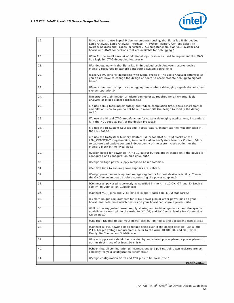
19. “If you want to use Signal Probe incremental routing, the SignalTap II EmbeddedLogic Analyzer, Logic Analyzer Interface, In-System Memory Content Editor, In-System Sources and Probes, or Virtual JTAG megafunction, plan your system andboard with JTAG connections that are available for debugging.”
20. “Plan for the small amount of additional logic resources used to implement the JTAGhub logic for JTAG debugging features.”
21. “For debugging with the SignalTap II Embedded Logic Analyzer, reserve devicememory resources to capture data during system operation.”
22. “Reserve I/O pins for debugging with Signal Probe or the Logic Analyzer Interface soyou do not have to change the design or board to accommodate debugging signalslater.”
23. “Ensure the board supports a debugging mode where debugging signals do not affectsystem operation.”
24. “Incorporate a pin header or mictor connector as required for an external logicanalyzer or mixed signal oscilloscope.”
25. “To use debug tools incrementally and reduce compilation time, ensure incrementalcompilation is on so you do not have to recompile the design to modify the debugtool.”
26. “To use the Virtual JTAG megafunction for custom debugging applications, instantiateit in the HDL code as part of the design process.”
27. “To use the In-System Sources and Probes feature, instantiate the megafunction inthe HDL code.”
28. “To use the In-System Memory Content Editor for RAM or ROM blocks or theLPM_CONSTANT megafunction, turn on the Allow In-System Memory Content Editorto capture and update content independently of the system clock option for thememory block in the IP catalog.”
29. “Design board for power-up: Arria 10 output buffers are tri-stated until the device isconfigured and configuration pins drive out.”
30. “Design voltage power supply ramps to be monotonic.”
31. “Set POR time to ensure power supplies are stable.”
32. “Design power sequencing and voltage regulators for best device reliability. Connectthe GND between boards before connecting the power supplies.”
33. “Connect all power pins correctly as specified in the Arria 10 GX, GT, and SX DeviceFamily Pin Connection Guidelines.”
34. “Connect VCCIO pins and VREF pins to support each bank’s I/O standards.”
35. “Explore unique requirements for FPGA power pins or other power pins on yourboard, and determine which devices on your board can share a power rail.”
36. “Follow the suggested power supply sharing and isolation guidance, and the specificguidelines for each pin in the Arria 10 GX, GT, and SX Device Family Pin ConnectionGuidelines.”
37. “Use the PDN tool to plan your power distribution netlist and decoupling capacitors.”
38. “Connect all PLL power pins to reduce noise even if the design does not use all thePLLs. For pin voltage requirements, refer to the Arria 10 GX, GT, and SX DeviceFamily Pin Connection Guidelines.”
39. “Power supply nets should be provided by an isolated power plane, a power plane cutout, or thick trace of at least 20 mils.”
40. “Check that all configuration pin connections and pull-up/pull-down resistors are setcorrectly for your configuration scheme(s).”
41. “Design configuration DCLK and TCK pins to be noise-free.”
continued...
1 AN 738: Intel® Arria® 10 Device Design Guidelines
AN 738: Intel® Arria® 10 Device Design Guidelines59

42. “Connect JTAG pins to a stable voltage level if not in use.”
43. “Connect JTAG pins correctly to the download cable header. Ensure the pin order isnot reversed.”
44. “To disable the JTAG state machine during power-up, pull the TCK pin low through a1-kW resistor to ensure that an unexpected rising edge does not occur on TCK.”
45. “Pull TMS and TDI high through a 1-k to 10-kW resistor.”
46. “Connect TRST directly to VCCPGM (Connecting the pin low disables the JTAGcircuitry).”
47. “Because the download cable interfaces with the JTAG pins of your device, ensure thedownload cable and JTAG pin voltages are compatible.”
48. “Buffer JTAG signals per the recommendations, especially for connectors or if thecable drives more than three devices.”
49. “If your device is in a configuration chain, ensure all devices in the chain areconnected properly.”
50. “Connect the MSEL pins to a select configuration scheme; do not leave them floating.For flexibility to change between configuration modes during testing or debugging,set up the board to connect each pin to either VCCPGM or GND without pull-up or pull-down resistors.”
51. “Connect nIO_PULLUP directly to GND.”
52. “Hold the nCE (chip enable) pin low during configuration, initialization, and usermode.”
53. “Turn on the device-wide output enable option, if required.”
54. “Specify the reserved state for unused I/O pins.”
55. “Carefully check the pin connections in the Quartus Prime software-generated .pin.Do not connect RESERVED pins.”
56. “Design VREF pins to be noise-free.”
57. “Break out large bus signals on board layers close to the device to reduce cross talk.”
58. “Route traces orthogonally if two signal layers are next to each other, if possible. Usea separation of 2 to 3 times the trace width.”
59. “Check I/O termination and impedance matching for chosen I/O standards, especiallyfor voltage-referenced standards.”
60. “Perform board-level simulation using IBIS models (when available).”
61. “Configure board trace models for Quartus Prime advanced I/O timing analysis.”
62. “Use the Quartus Prime Pin Planner to make pin assignments.”
63. “Use Quartus Prime Fitter messages and reports for sign-off of pin assignments.”
64. “Verify that the Quartus Prime pin assignments match those in the schematic andboard layout tools.”
65. “Use the Create Top-Level Design File command with I/O Assignment Analysis tocheck the I/O assignments before the design is complete.”
66. “Plan the I/O signaling type based on the system requirements.”
67. “Allow the software to assign locations for the negative pin in differential pin pairs.”
68. “Select a suitable signaling type and I/O standard for each I/O pin. The I/O banksare located in I/O columns. Each I/O bank contains its own PLL, DPA, and SERDEScircuitries.”
continued...
1 AN 738: Intel® Arria® 10 Device Design Guidelines
AN 738: Intel® Arria® 10 Device Design Guidelines60
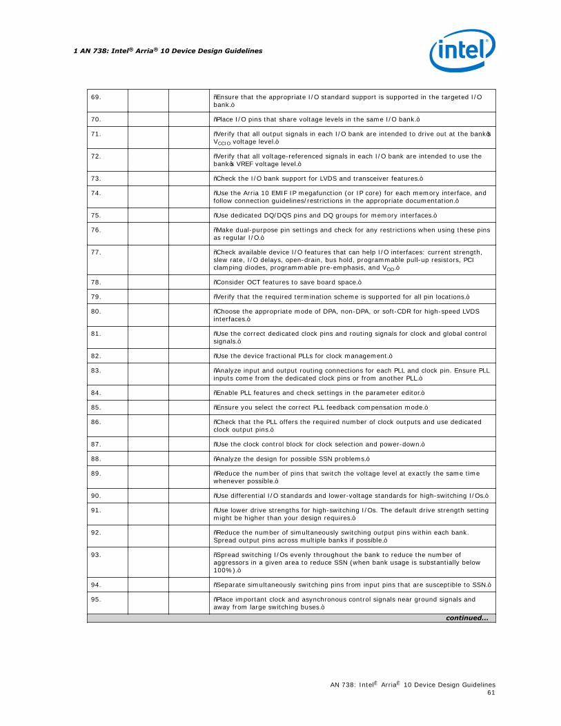
69. “Ensure that the appropriate I/O standard support is supported in the targeted I/Obank.”
70. “Place I/O pins that share voltage levels in the same I/O bank.”
71. “Verify that all output signals in each I/O bank are intended to drive out at the bank’sVCCIO voltage level.”
72. “Verify that all voltage-referenced signals in each I/O bank are intended to use thebank’s VREF voltage level.”
73. “Check the I/O bank support for LVDS and transceiver features.”
74. “Use the Arria 10 EMIF IP megafunction (or IP core) for each memory interface, andfollow connection guidelines/restrictions in the appropriate documentation.”
75. “Use dedicated DQ/DQS pins and DQ groups for memory interfaces.”
76. “Make dual-purpose pin settings and check for any restrictions when using these pinsas regular I/O.”
77. “Check available device I/O features that can help I/O interfaces: current strength,slew rate, I/O delays, open-drain, bus hold, programmable pull-up resistors, PCIclamping diodes, programmable pre-emphasis, and VOD.”
78. “Consider OCT features to save board space.”
79. “Verify that the required termination scheme is supported for all pin locations.”
80. “Choose the appropriate mode of DPA, non-DPA, or soft-CDR for high-speed LVDSinterfaces.”
81. “Use the correct dedicated clock pins and routing signals for clock and global controlsignals.”
82. “Use the device fractional PLLs for clock management.”
83. “Analyze input and output routing connections for each PLL and clock pin. Ensure PLLinputs come from the dedicated clock pins or from another PLL.”
84. “Enable PLL features and check settings in the parameter editor.”
85. “Ensure you select the correct PLL feedback compensation mode.”
86. “Check that the PLL offers the required number of clock outputs and use dedicatedclock output pins.”
87. “Use the clock control block for clock selection and power-down.”
88. “Analyze the design for possible SSN problems.”
89. “Reduce the number of pins that switch the voltage level at exactly the same timewhenever possible.”
90. “Use differential I/O standards and lower-voltage standards for high-switching I/Os.”
91. “Use lower drive strengths for high-switching I/Os. The default drive strength settingmight be higher than your design requires.”
92. “Reduce the number of simultaneously switching output pins within each bank.Spread output pins across multiple banks if possible.”
93. “Spread switching I/Os evenly throughout the bank to reduce the number ofaggressors in a given area to reduce SSN (when bank usage is substantially below100%).”
94. “Separate simultaneously switching pins from input pins that are susceptible to SSN.”
95. “Place important clock and asynchronous control signals near ground signals andaway from large switching buses.”
continued...
1 AN 738: Intel® Arria® 10 Device Design Guidelines
AN 738: Intel® Arria® 10 Device Design Guidelines61
96. “Avoid using I/O pins one or two pins away from PLL power supply pins for high-switching or high-drive strength pins.”
97. “Use staggered output delays to shift the output signals through time, or useadjustable slew rate settings.”
98. “Use synchronous design practices. Pay attention to clock signals.”
99. “Use the Quartus II Design Assistant to check design reliability.”
99. “Use megafunctions with the parameter editor.”
100. “Follow recommended coding styles, especially for inferring device dedicated logicsuch as memory and DSP blocks.”
101. “Enable the chip-wide reset to clear all registers if required.”
102. “Consider resources available for register power-up and control signals. Do not applyboth reset and preset signals to a register.”
103. “Follow recommendations to set up your source code and partition your design forincremental compilation; plan early in the design flow.”
104. “Perform timing budgeting and resource balancing between partitions to achieve bestresults, especially in team-based flows.”
105. “Create a design floorplan for incremental compilation partitions, if required for yourdesign flow.”
106. “Specify your third-party synthesis tool and use the correct supported version.”
107. “Review resource utilization reports after compilation.”
108. “Review all Quartus Prime messages, especially warning or error messages.”
109. “Ensure timing constraints are complete and accurate, including all clock signals andI/O delays.”
110. “Review the TimeQuest Timing Analyzer reports after compilation to ensure there areno timing violations.”
111. “Ensure that the input I/O times are not violated when data is provided to the Arria10 device.”
112. “Turn on Optimize multi-corner timing on the Fitter Settings page in theSettings dialog box.”
113. “Use create_clock and create_generated_clock to specify the frequencies andrelationships for all clocks in your design.”
114. “Use set_input_delay and set_output_delay to specify the external device orboard timing parameters.”
115. “Use derive_pll_clocks to create generated clocks for all PLL outputs, accordingto the settings in the PLL megafunctions. Specify multicycle relationships for LVDStransmitters or receiver deserialization factors.”
116. “Use derive_clock_uncertainty to automatically apply inter-clock, intra-clock,and I/O interface uncertainties.”
117. “Use check_timing to generate a report on any problem with the design or appliedconstraints, including missing constraints.”
118. “Perform Early Timing Estimation if you want timing estimates before running a fullcompilation.”
119. “Use Quartus Prime optimization features to achieve timing closure or improve theresource utilization.”
120. “Use the Timing and Area Optimization Advisors to suggest optimization settings.”
continued...
1 AN 738: Intel® Arria® 10 Device Design Guidelines
AN 738: Intel® Arria® 10 Device Design Guidelines62

121. “Use incremental compilation to preserve performance for unchanged blocks in yourdesign and to reduce compilation times.”
122. “Ensure parallel compilation is enabled if you have multiple processors available forcompilation.”
123. “Use the Compilation Time Advisor to suggest settings that reduce compilation time.”
124. “Specify your third-party simulation tool, and use the correct supported version andsimulation models.”
125. “Specify your third-party formal verification tool and use the correct supportedversion.”
126. “If you use formal verification, check for support and design limitations.”
127. “After compilation, analyze power consumption and heat dissipation in the PowerAnalyzer.”
128. “Provide accurate typical signal activities, preferably with a gate-levelsimulation .vcd, to get accurate power analysis results.”
129. “Specify the correct operating conditions for power analysis.”
130. “Use recommended design techniques and Quartus Prime options to optimize yourdesign for power consumption, if required.”
131. “Use the Power Optimization Advisor to suggest optimization settings.”
1 AN 738: Intel® Arria® 10 Device Design Guidelines
AN 738: Intel® Arria® 10 Device Design Guidelines63

1.11 Appendix: Arria 10 Transceiver Design Guidelines
Figure 2. Arria 10 FPGA Architecture Block Diagram
Core
Logic
Fabr
ic
M20
K Int
erna
l Mem
ory B
locks
Trans
ceive
r Cha
nnels
Hard
IP Pe
r Tra
nsce
iver:
Stan
dard
PCS,
PCIe
Gen 3
PCS,
Enha
nced
PCS
PCI E
xpre
ss Ge
n3 H
ard I
P PL
Ls
M20
K Int
erna
l Mem
ory B
locks
PCI E
xpre
ss Ge
n3 H
ard I
P
Varia
ble Pr
ecisi
on D
SP Bl
ocks
I/O PL
LsHa
rd M
emor
y Con
trolle
rs, G
ener
al-Pu
rpos
e I/O
Cells
, LVD
S
M20
K Int
erna
l Mem
ory B
locks
M20
K Int
erna
l Mem
ory B
locks
Varia
ble Pr
ecisi
on D
SP Bl
ocks
Core
Logic
Fabr
ic I/O PL
LsHa
rd M
emor
y Con
trolle
rs, G
ener
al-Pu
rpos
e I/O
Cells
, LVD
S
M20
K Int
erna
l Mem
ory B
locks
M20
K Int
erna
l Mem
ory B
locks
Varia
ble Pr
ecisi
on D
SP Bl
ocks
Trans
ceive
r Cha
nnels
PCI E
xpre
ss Ge
n3 H
ard I
PPC
I Exp
ress
Gen3
Har
d IP
PLLs
Hard
IP Pe
r Tra
nsce
iver:
Stan
dard
PCS,
PCIe
Gen 3
PCS,
Enha
nced
PCS
Arria 10 Transceivers Arria 10 Transceivers
Note: The transceiver channels are placed on the left side periphery in most Arria 10devices. For larger Arria 10 devices, additional transceiver channels are placed on theright side periphery.
1.11.1 Transceiver PHY Architecture Overview
A link is defined as a single entity communication port. A link can have one or moretransceiver channels. A transceiver channel is synonymous with a transceiver lane.
For example, a 10GBASE-R link has one transceiver channel or lane with a data rate of10.3125 Gbps. A 40GBASE-R link has four transceiver channels. Each transceiverchannel operates at a lane data rate of 10.3125 Gbps. Four transceiver channels givea total collective link bandwidth of 41.25 Gbps (40 Gbps before and after 64B/66B PCSencoding and decoding).
1 AN 738: Intel® Arria® 10 Device Design Guidelines
AN 738: Intel® Arria® 10 Device Design Guidelines64

1.11.2 Transceiver Bank Architecture
The transceiver bank is the fundamental unit that contains all the functional blocksrelated to the device's high speed serial transceivers.
Each transceiver bank includes six transceiver channels in all devices except for thedevices with 66 transceiver channels. These devices (with 66 transceiver channels)have both six channel and three channel transceiver banks. The uppermost transceiverbank on the left and the right side of these devices is a three channel transceiverbank. All other devices contain six channel transceiver banks.
The figures below show the transceiver bank architecture with the phase locked loop(PLL) and clock generation block (CGB) resources available in each bank.
Figure 3. Three-Channel GX Transceiver Bank Architecture
PMAChannel PLL(CDR Only)
PCS
Local CGB2
CH2
PMAChannel PLL(CMU/CDR)
PCS
Local CGB1
CH1
PMAChannel PLL(CDR Only)
PCS
Local CGB0
CH0
FPGA CoreFabric
Three-Channel GX Transceiver Bank
MasterCGB0
fPLL0
ATXPLL0
ClockDistribution
Network
1 AN 738: Intel® Arria® 10 Device Design Guidelines
AN 738: Intel® Arria® 10 Device Design Guidelines65

Figure 4. Six-Channel GX Transceiver Bank Architecture
PMAChannel PLL(CDR Only)
PCS
Local CGB5
CH5
PMAChannel PLL(CMU/CDR)
PCS
Local CGB4
CH4
PMAChannel PLL(CDR Only)
PCS
Local CGB3
CH3
PMAChannel PLL(CDR Only)
PCS
Local CGB2
CH2
PMAChannel PLL(CMU/CDR)
PCS
Local CGB1
CH1
PMAChannel PLL(CDR Only)
PCS
Local CGB0
CH0
FPGA CoreFabric
ClockDistribution
NetworkSix-Channel GX Transceiver Bank
fPLL1
MasterCGB1
MasterCGB0
ATXPLL0
ATXPLL1
fPLL0
1 AN 738: Intel® Arria® 10 Device Design Guidelines
AN 738: Intel® Arria® 10 Device Design Guidelines66

Figure 5. GT Transceiver Bank Architecture for Bank GXBL1G
CH1
PMAChannel PLL(CDR Only)
PCS
Local CGB5
CH5
PMAChannel PLL(CMU/CDR)
PCS
Local CGB4
CH4
PMAChannel PLL(CDR Only)
PCS
Local CGB3
CH3
PMAChannel PLL(CDR Only)
PCS
Local CGB2
CH2
PMAChannel PLL(CMU/CDR)
PCS
Local CGB1
PMAChannel PLL(CDR Only)
PCS
Local CGB0
CH0
FPGA CoreFabric
ClockDistribution
NetworkSix-Channel GT Transceiver Bank GXBL1G
fPLL1
MasterCGB1
MasterCGB0
ATXPLL1
ATXPLL0
fPLL0
GX ChannelGT/GX ChannelLegend
1 AN 738: Intel® Arria® 10 Device Design Guidelines
AN 738: Intel® Arria® 10 Device Design Guidelines67

Note: In GT devices, the transceiver banks GXBL1E, GXBL1G, and GXBL1H include GTchannels.
1 AN 738: Intel® Arria® 10 Device Design Guidelines
AN 738: Intel® Arria® 10 Device Design Guidelines68

Figure 6. GT Transceiver Bank Architecture for Banks GXBL1E and GXBL1H
CH1
PMAChannel PLL(CDR Only)
PCS
Local CGB5
CH5
PMAChannel PLL(CMU/CDR)
PCS
Local CGB4
CH4
PMAChannel PLL(CDR Only)
PCS
Local CGB3
CH3
PMAChannel PLL(CDR Only)
PCS
Local CGB2
CH2
PMAChannel PLL(CMU/CDR)
PCS
Local CGB1
PMAChannel PLL(CDR Only)
PCS
Local CGB0
CH0
FPGA CoreFabric
ClockDistribution
NetworkSix-Channel GTTransceiver Banks GXBL1E and GXBL1H
fPLL1
MasterCGB1
MasterCGB0
ATXPLL1
ATXPLL0
fPLL0
GX ChannelGT/GX ChannelLegend
1 AN 738: Intel® Arria® 10 Device Design Guidelines
AN 738: Intel® Arria® 10 Device Design Guidelines69

The transceiver channels perform all the required PHY layer functions between theFPGA fabric and the physical medium. The high speed clock required by thetransceiver channels is generated by the transceiver PLLs. The master and local clockgeneration blocks (CGBs) provide the necessary high speed serial and low speedparallel clocks to drive the non-bonded and bonded channels in the transceiver bank.
Related Links
Transceiver BasicsFor an online training course for transceivers
1.11.3 PHY Layer Transceiver Components
Transceivers in Arria 10 devices support both Physical Medium Attachment (PMA) andPhysical Coding Sublayer (PCS) functions at the physical (PHY) layer.
A PMA is the transceiver's electrical interface to the physical medium. The transceiverPMA consists of standard blocks such as:
• serializer/deserializer (SERDES)
• clock and data recovery PLL
• analog front end transmit drivers
• analog front end receive buffers
The PCS can be bypassed with a PCS-Direct configuration. Both the PMA and PCSblocks are fed by multiple clock networks driven by high performance PLLs. In PCS-Direct configuration, the data flow is through the PCS block, but all the internal PCSblocks are bypassed. In this mode, the PCS functionality is implemented in the FPGAfabric.
1.11.3.1 The GX Transceiver Channel
Related Links
• PLLsFor more information about transceiver PLLs in Arria 10 devices
• ATX PLLFor more information about ATX PLL
• ATX PLL IPFor details about implementing the ATX PLL IP
• fPLLFor more information about fPLL
• fPLL IPFor details about implementing the fPLL IP
• CMU PLLFor more information about CMU PLL
• CMU PLL IPFor details about implementing the CMU PLL IP
• Clock Generation BlockFor more information about the clock generation block
• design examples
1 AN 738: Intel® Arria® 10 Device Design Guidelines
AN 738: Intel® Arria® 10 Device Design Guidelines70
For more information about design examples
• CPRI MegaCore Function User GuideFor more information about the Arria 10 protocols
• DisplayPort IP Core Function User GuideFor more information about the Arria 10 protocols
• Low Latency 40- and 100-Gbps Ethernet MAC and PHY MegaCore Function UserGuide
For more information about the Arria 10 protocols
• 100G Interlaken MegaCore Function User GuideFor more information about the Arria 10 and Interlaken
• 50G Interlaken MegaCore Function User GuideFor more information about the Arria 10 and Interlaken
• Arria 10 Avalon-MM DMA Interface for PCIe* Solutions User GuideFor more information about the Arria 10 and PCIe*
• Arria 10 Avalon-MM Interface for PCIe Solutions User GuideFor more information
• Arria 10 Avalon-ST Interface for PCIe Solutions User GuideFor more information
• SerialLite III Streaming MegaCore Function User GuideFor more information
• RapidIO II MegaCore Function User GuideFor more information
1.11.3.2 The GT Transceiver Channel
The GT transceiver channels are used for supporting data rates from 17.4 Gbps to25.8 Gbps. The GT transceiver channels can also be reconfigured as GX transceiverchannels. When they are reconfigured as GX transceiver channels, the Standard PCS,Enhanced PCS, and PCIe Gen3 PCS are available and they support data rates from1 Gbps to 17.4 Gbps.
1 AN 738: Intel® Arria® 10 Device Design Guidelines
AN 738: Intel® Arria® 10 Device Design Guidelines71

Figure 7. GT Transceiver Channel in Full Duplex Mode Operating Between 17.4 Gbpsand 25.8 Gbps
Notes:
(3) The Standard PCS and PCIe Gen3 PCS blocks are available when the GT channel is reconfigured as a GX transceiver channel.
(1) The Enhanced PCS must be configured in lowl latency mode to support data rate range from 17.4 Gbps to 25.8 Gbps.(2) The FPGA Fabric - PCS and PCS-PMA interface widths are configurable.
Standard PCS
PCIe Gen3 PCS
Enhanced PCSKR FEC
PCS Direct
FPGA FabricTransmitter PCSTransmitter PMA
Serializer
Standard PCS
PCIe Gen3 PCS
Enhanced PCSKR FEC
PCS Direct
Receiver PCSReceiver PMA
DeserializerCDR
(1)
(1)
(2)
(2)
(2)
(2) (3)
(3)
(3)
(3)
Table 67. PCS Types and Data Rates Supported by GT Channel Configurations
GT Channel Configuration PCS Type Data Rates Supported
GT Standard PCS Not available
Enhanced PCS 17.4 Gbps to 25.8 Gbps (1)
PCIe Gen3 PCS Not available
GX Standard PCS 1 Gbps to 10 Gbps
Enhanced PCS 1 Gbps to 17.4 Gbps
PCIe Gen3 PCS 8 Gbps
Notes:1. The Enhanced PCS must be configured in low latency mode to support data rate range from 17.4 Gbps to 25.8 Gbps.2. The GT channels can also operate in PCS-Direct configuration for data rates between 1 Gbps to 25.8 Gbps.
1.11.4 Transceiver Phase-Locked Loops
Each transceiver channel in Arria 10 devices has direct access to three types of highperformance PLLs:
• Advanced Transmit (ATX) PLL
• Fractional PLL (fPLL)
• Channel PLL / Clock Multiplier Unit (CMU) PLL.
1 AN 738: Intel® Arria® 10 Device Design Guidelines
AN 738: Intel® Arria® 10 Device Design Guidelines72
These transceiver PLLs along with the Master or Local Clock Generation Blocks (CGB)drive the transceiver channels.
Related Links
Arria 10 Transceiver PHY User GuideFor more information about transceiver PLLs in Arria 10 devices, refer to the "PLLs"section of the "PLLs and Clock Networks" chapter of this user guide
1.11.4.1 Advanced Transmit (ATX) PLL
An advanced transmit (ATX) PLL is a high performance PLL. It supports both integerfrequency synthesis and coarse resolution fractional frequency synthesis. The ATX PLLis the transceiver channel’s primary transmit PLL. It can operate over the full range ofsupported data rates required for high data rate applications.
Related Links
• Arria 10 Transceiver PHY User GuideFor more information about ATX PLL, refer to the "ATX PLL" section of the "PLLsand Clock Networks" chapter of this user guide
• Arria 10 Transceiver PHY User GuideFor details about implementing the ATX PLL IP, refer to the "ATX PLL IP" sectionof the "PLLs and Clock Networks" chapter of this user guide
1.11.4.2 Fractional PLL (fPLL)
A fractional PLL (fPLL) is an alternate transmit PLL used for generating low clockfrequencies for low data rate applications. fPLLs support both integer frequencysynthesis and fine resolution fractional frequency synthesis. Unlike the ATX PLL, thefPLL can be used to synthesize frequencies that can drive the core through the FPGAfabric clock networks.
Related Links
• Arria 10 Transceiver PHY User GuideFor more information about fPLL, refer to the "fPLL" section of the "PLLs andClock Networks" chapter of this user guide
• Arria 10 Transceiver PHY User GuideFor details about implementing the fPLL IP, refer to the "fPLL IP" section of the"PLLs and Clock Networks" chapter of this user guide
1.11.4.3 Channel PLL (CMU/CDR PLL)
A channel PLL resides locally within each transceiver channel. Its primary function isclock and data recovery in the transceiver channel when the PLL is used in CDR mode.The channel PLLs of channel 1 and 4 can be used as a transmit PLL when reconfiguredin CMU mode. The channel PLLs of channel 0, 2, 3, and 5 cannot be reconfigured inCMU mode and therefore cannot be used as a transmit PLL.
Related Links
• Arria 10 Transceiver PHY User GuideFor more information about CMU PLL, refer to the "CMU PLL" section of the"PLLs and Clock Networks" chapter in this user guide
1 AN 738: Intel® Arria® 10 Device Design Guidelines
AN 738: Intel® Arria® 10 Device Design Guidelines73
• Arria 10 Transceiver PHY User GuideFor details about implementing the CMU PLL IP, refer to the "CMU PLL IP"section of the "PLLs and Clock Networks" chapter of this user guide
1.11.5 Clock Generation Block (CGB)
In Arria 10 devices, there are two types of clock generation blocks (CGBs):
• Master CGB
• Local CGB
Transceiver banks with six transceiver channels have two master CGBs. Master CGB1is located at the top of the transceiver bank and master CGB0 is located at the bottomof the transceiver bank. Transceiver banks with three channels have only one masterCGB. The master CGB divides and distributes bonded clocks to a bonded channelgroup. It also distributes non-bonded clocks to non-bonded channels across the x6/xNclock network.
Each transceiver channel has a local CGB. The local CGB is used for dividing anddistributing non-bonded clocks to its own PCS and PMA blocks.
Related Links
Arria 10 Transceiver PHY User GuideFor more information about the clock generation block, refer to the "ClockGeneration Block" section of the "PLLs and Clock Networks" chapter in this userguide
1.11.6 Calibration
Arria 10 FPGA devices contain a dedicated calibration engine to compensate forprocess variations.
The calibration engine calibrates the analog portion of the transceiver to allow boththe transmitter and receiver to operate at maximum performance. Each Arria 10device contains two calibration engines and each engine resides on either side of thedevice. A hard NIOS II processor controls the calibration flow.
The CLKUSR pin clocks the calibration engine. All transceiver reference clocks and theCLKUSR clock must be free running and stable upon device power-up to successfullycomplete the calibration process and for optimal transceiver performance.
Related Links
• Arria 10 Device DatasheetFor more information about CLKUSR pin requirements
• Configuration, Design Security, and Remote System Upgrades in Arria 10 DevicesFor information about configuration requirements for the CLKUSR pin
1 AN 738: Intel® Arria® 10 Device Design Guidelines
AN 738: Intel® Arria® 10 Device Design Guidelines74

1.11.7 Transceiver Design Flow
Figure 8. Transceiver Design Flow
Generate PHY IP Core
Connect Transceiver Datapath to MAC IP Core or to a Data Generator / Analyzer
Select PLL IP CoreGenerate the Transceiver PHY Reset Controller IP Core
or create your own User-Coded Reset Controller
Compile Design
Verify Design Functionality
Generate PLL IP Core
Configure the PHY IP Core
Select PHY IP Core
Configure the PLL IP Core
Connect PHY IP Core to PLL IP Core, Reset Controller, and connect reconfiguration logic via Avalon-MM interface
Create reconfiguration logic (if needed)
Make Pin Assignments Using Pin Planner and Assignment Editor or in the Quartus Settings File (QSF)
Related Links
• Arria 10 Transceiver PHY Design ExamplesFor more information about design examples refer to the Intel FPGA Wiki pagethat provides useful guidance for developing your own design. However, thewiki is not guaranteed by Intel.
• CPRI MegaCore Function User Guide
• DisplayPort IP Core Function User Guide
• Low Latency 40- and 100-Gbps Ethernet MAC and PHY MegaCore Function UserGuide
• 100G Interlaken MegaCore Function User Guide
• 50G Interlaken MegaCore Function User Guide
• Arria 10 Avalon-MM DMA Interface for PCIe* Solutions User Guide
1 AN 738: Intel® Arria® 10 Device Design Guidelines
AN 738: Intel® Arria® 10 Device Design Guidelines75

• Arria 10 Avalon-MM Interface for PCIe Solutions User Guide
• Arria 10 Avalon-ST Interface for PCIe Solutions User Guide
• SerialLite III Streaming MegaCore Function User Guide
• RapidIO II MegaCore Function User Guide
1 AN 738: Intel® Arria® 10 Device Design Guidelines
AN 738: Intel® Arria® 10 Device Design Guidelines76


