22
AN 900: Intel ® Arria 10 DisplayPort 8K RX-only Design Subscribe Send Feedback AN-900 | 2021.07.02 Latest document on the web: PDF | HTML

AN 900: Intel® Arria 10 DisplayPort8K RX-only Design
SubscribeSend Feedback
AN-900 | 2021.07.02Latest document on the web: PDF | HTML

Contents
1. Intel® Arria® 10 DisplayPort 8K RX-only Design............................................................. 31.1. Design Components............................................................................................... 41.2. Clocking Scheme................................................................................................... 51.3. Top Level Interface Signals..................................................................................... 61.4. Quick Start Guide ................................................................................................. 7
1.4.1. Hardware and Software Requirements.......................................................... 71.4.2. Directory Structure.................................................................................... 71.4.3. Compiling the Design ................................................................................ 81.4.4. Running the Design on Hardware............................................................... 101.4.5. Design Debug Features.............................................................................13
1.5. Creating the RX-only Design..................................................................................161.5.1. Generating the Design.............................................................................. 161.5.2. Removing Irrelevant Blocks....................................................................... 171.5.3. Making a Direct Connection to the RX Transceiver Block................................ 191.5.4. Selecting the Bitec FMC Daughter Card Revision...........................................211.5.5. Modifying the Software............................................................................. 21
1.6. Document Revision History for AN 900: Intel Arria 10 DisplayPort 8K RX-only Design....22
Contents
AN 900: Intel® Arria 10 DisplayPort 8K RX-only Design Send Feedback
2

1. Intel® Arria® 10 DisplayPort 8K RX-only DesignThe Intel® Arria® 10 8K DisplayPort RX-only design demonstrates how the DisplayPortsink (RX) receives video input generated by the video source through the Bitec FMCdaughter card.
This design uses local Extended Display Identification Data (EDID) information toinform the source device its capabilities during Link Training process. The designenables the DisplayPort sink to receive a wide range of input video resolution fromGPU, up to a maximum of 8K, 30Hz video resolution.
Figure 1. Intel Arria 10 DisplayPort 8K RX-only Design Block Diagram
Debug FIFO
PIO
RX AUX TransactionMonitoring
LEDIndicator
MSA Print Push Button 0
Computer
OC RAM NIOS II Processor
12C MasterSlave Translator
SYSIDTimer
JTAG UART
Core System (Qsys)
SinkManagementRX AUX Debug
Stream
Avalon-MMInterconnect
DisplayPort RXManagement Bridge
DisplayPort RXCore
RX ReconfigurationManagement
100 MHzReference ClockReset Button
Top
Transceiver NativePHY
RX Reconfiguration
Transceiver PHYReset Controller
RX Sub-system (Qsys)
Avalon-MMInterconnect
Video PLL
RX PHY Top
135 MHz CDR Ref Clk
Bitec FMC Daughter Card
Top level design
Intel FPGA IP componentsoutside Qsys system
Intel FPGA IP componentsinside dp_core Qsys system
Intel FPGA IP componentsinside DP RX Qsys system
Custom logic components
16 MHz
300 MHz
Locked
Reset Generator
AN-900 | 2021.07.02
Send Feedback
Intel Corporation. All rights reserved. Intel, the Intel logo, and other Intel marks are trademarks of IntelCorporation or its subsidiaries. Intel warrants performance of its FPGA and semiconductor products to currentspecifications in accordance with Intel's standard warranty, but reserves the right to make changes to anyproducts and services at any time without notice. Intel assumes no responsibility or liability arising out of theapplication or use of any information, product, or service described herein except as expressly agreed to inwriting by Intel. Intel customers are advised to obtain the latest version of device specifications before relyingon any published information and before placing orders for products or services.*Other names and brands may be claimed as the property of others.
ISO9001:2015Registered

Related Information
• Intel Design StoreProvides the design files.
• DisplayPort Intel Arria 10 FPGA IP Design Example User GuideProvides more information about the Intel Arria 10 design examples.
1.1. Design Components
The DisplayPort Intel FPGA IP design example requires these components.
Table 1. Core System Components
Module Description
Core System (Platform Designer) The core system consists of the Nios® II processor and its necessarycomponents, and the DisplayPort RX core sub-systems.This system provides the infrastructure to interconnect the Nios II processor withthe DisplayPort Intel FPGA IP (RX instance) through Avalon® memory-mappedinterface within a single Platform Designer system to ease the software buildflow.This system consists of:• CPU Sub-system• RX Sub-system
RX Sub-system (Platform Designer) The RX sub-system consists of:• Clock Source—The clock source to the DisplayPort RX core. This sub-system
has two clock integrated sources: 300 MHz and 16 MHz.• Reset Bridge—The bridge that connects the external signal to the sub-system.
This bridge synchronizes to a respective clock source before it is used.• DisplayPort RX core—DisplayPort sink core, VESA DisplayPort Standard
version 1.4.• Debug FIFO—This FIFO captures all DisplayPort RX auxiliary cycles, and prints
out in the Nios II Debug terminal.• PIO—The parallel IO that triggers the Main Stream Attribute (MSA) captured
and prints out when you press the onboard push button..• Avalon Memory-Mapped Pipeline Bridge—This bridge interconnects the Avalon
memory-mapped interface between components within the RX sub-system tothe Nios II processor in the Core sub-system.
• EDID—The EDID RAM stores the desired EDID values in the RAM andconnects to DisplayPort sink core. The design uses this component only whenyou turn off the Enable GPU Control option in the RX core.
Table 2. DisplayPort RX PHY Top Components
Module Description
RX PHY Top The RX PHY top level consists of the components related to the receiver PHYlayer.• Transceiver Native PHY(RX)—The hard transceiver block that receives the
serial data from an external video and deserializes it to 20-bit or 40-bitparallel data for the DisplayPort Intel FPGA IP sink core.
• Transceiver PHY Reset Controller—The RX Reconfiguration Managementmodule triggers the reset input of this controller to generate thecorresponding analog and digital reset signals to the Transceiver Native PHYblock according to the reset sequencing.
• RX Reconfiguration Management—This block reconfigures and recalibrates theTransceiver Native PHY to receive serial data in the supported data rates(RBR, HBR, HBR2, and HBR3).
Note: 8.1 Gbps is available only in the Intel Quartus® Prime Pro Editionsoftware.
1. Intel® Arria® 10 DisplayPort 8K RX-only Design
AN-900 | 2021.07.02
AN 900: Intel® Arria 10 DisplayPort 8K RX-only Design Send Feedback
4

Table 3. Top-Level Common Block
Module Description
Video PLL IOPLL generates two common source clocks:• 300 MHz—Used as DisplayPort RX sink video clock source.• 16 MHz—Used as DisplayPort RX auxiliary clock.
1.2. Clocking Scheme
The clocking scheme illustrates the clock domains in the DisplayPort Intel FPGA IPdesign example.
Table 4. Clocking Scheme Signals
Clock Signal Name in Design Description
RX PLL Refclock rx_cdr_refclk 135 MHz transceiver clock data recovery (CDR) referenceclock that is divisible by the transceiver for all DisplayPortdata rates (1.62 Gbps, 2.7 Gbps, 5.4 Gbps, and 8.1 Gbps).Note: The reference clock source of the RX refclock is
located at the HSSI refclk pin.
RX Transceiver Clockout gxb_rx_clkout RX clock recovered from the transceiver, and the frequencyvaries depending on the data rate and symbols per clock.
Data Rate Symbols perClock
Frequency(MHz)
RBR (1.62 Gbps) 2 (dual) 81
4 (quad) 40.5
HBR (2.7 Gbps) 2 (dual) 135
4 (quad) 67.5
HBR2 (5.4 Gbps) 2 (dual) 270
4 (quad) 135
HBR3 (8.1 Gbps) 4 (quad) 202.5
Management Clock rx_rcfg_mgmt_clk A free running 100 MHz clock for both Avalon memory-mapped interfaces for reconfiguration and PHY resetcontroller for transceiver reset sequence.
Component RequiredFrequency
(MHz)
Avalon memory-mapped reconfiguration 100 – 125
Transceiver PHY reset controller 1 – 500
16 MHz Clock dp_rx_clk_16_in_clk 16 MHz clock used to encode and decode auxiliary channel inthe DisplayPort Intel FPGA IP sink core.
Calibration Clock dp_rx_clk_cal A 50 MHz calibration clock input that must be synchronous tothe Transceiver Reconfiguration module's clock. This clock isused in the DisplayPort Intel FPGA IP 's reconfiguration logic.
RX Video Clock dp_rx_dp_sink_rx_vid_clk
A 300 MHz video clock for DisplayPort sink to clock video datastream.
1. Intel® Arria® 10 DisplayPort 8K RX-only Design
AN-900 | 2021.07.02
Send Feedback AN 900: Intel® Arria 10 DisplayPort 8K RX-only Design
5

1.3. Top Level Interface Signals
The tables list the signals for the RX-only design example.
Table 5. On-board Oscillator Signal
Signal Direction Width Description
refclk1_p Input 1 100 MHz clock source used as IOPLL reference clock andAvalon memory-mapped management clock
Table 6. User Push Buttons and LEDs
Signal Direction Width Description
cpu_resetn Input 1 Global reset
user_pb Input 3 MSA prints out at user_pb[0]
user_led_g Output 8 User LED (data rate information)
Table 7. DisplayPort FMC Daughter Card Pins on FMC Port A
Signal Direction Width Description
fmca_gbtclk_m2c_p Input 2 135 MHz dedicated transceiver reference clock
fmca_dp_m2c_p Input 4 DisplayPort RX serial data
fmca_la_rx_p_6 Output 1 DisplayPort RX HPD• 1 = HPD asserted• 0 = HPD deasserted
fmca_la_tx_n_9 Input 1 DisplayPort RX Aux In
fmca_la_rx_n_6 Output 1 DisplayPort RX Aux Out
fmca_la_tx_p_9 Output 1 DisplayPort RX Aux OE
fmca_la_rx_n_8 Input 1 RX power detect (inverted)
fmca_la_tx_p_10 Input 1 RX cable detect
Table 8. FMC Onboard Retimer Reconfiguration Interface Signals
Signal Direction Width Description
Bitec FMC Revision 10 Bitec FMC Revision 11
fmca_la_tx_p_0 Inout 1 PS8460_SDA MCDP6000_SDA
fmca_la_tx_n_0 Inout 1 PS8460_SCL MCDP6000_SDL
fmca_la_rx_p_0 Output 1 PS8460_EQ0 Unused
fmca_la_rx_n_0 Output 1 PS8460_EQ1 Unused
fmca_la_tx_p_1 Output 1 PS8460_PDN Unused
fmca_la_tx_n_1 Output 1 PS8460_CFG0 Unused
fmca_la_tx_p_2 Output 1 PS8460_CFG1 Unused
fmca_la_tx_n_2 Output 1 PS8460_CFG2 Unused
1. Intel® Arria® 10 DisplayPort 8K RX-only Design
AN-900 | 2021.07.02
AN 900: Intel® Arria 10 DisplayPort 8K RX-only Design Send Feedback
6

1.4. Quick Start Guide
The reference design features a hardware design that supports compilation andhardware testing.
1.4.1. Hardware and Software Requirements
To test the design, ensure that you have the appropriate hardware and software.
Hardware
• Intel Arria 10 GX FPGA Development Kit (10AX115S2F45I1SG)
• Bitec FMC daughter card revision 8, 10 or 11
• GPU with 8K DisplayPort output as video source
• DisplayPort cables
Software
• Intel Quartus Prime Pro Edition version 19.2 (for hardware testing)
1.4.2. Directory Structure
The directory structure lists the folders and files needed for the design.
Table 9. Intel Arria 10 DisplayPort 8K RX-only Design Directory StructureThe 8K DisplayPort RX-only design file (A10_DP_RX_FMC_PRO.par) has the Additional_Files.zip filethat contains the master image and other software files. Unzip the Additional_Files.zip file andrestructure the folders accordingly based on the table below.
Folder File/Folder
Main top.qpf
top.qsf
rtl/
script/ (extracted from Additional_Files.zip)
software/ (extracted from Additional_Files.zip)
Additional_Files/ (extracted from Additional_Files.zip)
ReadMe.txt
DP_RX.stp
rtl/ a10_dp_demo.v
reset_gen.sv
bitec_reconfig_alt_a10.v
video_pll_a10.ip
reset_sync.sv
example.sdc
rtl/core/ dp_rx.qsys
continued...
1. Intel® Arria® 10 DisplayPort 8K RX-only Design
AN-900 | 2021.07.02
Send Feedback AN 900: Intel® Arria 10 DisplayPort 8K RX-only Design
7

Folder File/Folder
dp_core.qsys
<Platform Designer (Standard)-generated files and folder>
rtl/rx_phy/ gxb_rx.ip
gxb_rx_reset.ip
rx_phy_top.v
<Platform Designer (Standard)-generated files and folder>
rtl/video_pll_a10/ video_pll_a10.qip
<Platform Designer (Standard)-generated files and folder>
script build_ip.tcl
build_sw.sh
software/ <Other software files and folder>
software/dp_demo/ dp_demo.elf
main.c
config.h
rx_utils.c
debug.c
<Other software files and folder>
software/dp_demo_bsp/ alt_sys_init.c
linker.h
system.h
<Other software files and folder>
software/dp_demo_bsp/ <Other software files and folder>
software/dp_demo_bsp/ <Other software files and folder>
software/dp_demo_bsp/ <Other software files and folder>
Additional_Files/Master_Image/Rev_11
a10_dp_demo.sof
dp_demo.elf
1.4.3. Compiling the Design
You can download the DisplayPort 8K RX-only design file (A10_DP_RX_FMC_PRO.par)from the Intel Design Store. To compile and run a demonstration test on the hardwaredesign example using a Bitec Rev 11 card, follow these steps.
The .par file includes pre-compiled .sof files that you can run to test the design.
1. Intel® Arria® 10 DisplayPort 8K RX-only Design
AN-900 | 2021.07.02
AN 900: Intel® Arria 10 DisplayPort 8K RX-only Design Send Feedback
8

1. To extract the files in the .par file, refer to the Installation Package instruction inthe Intel Design Store design download page.
2. After extracting the .par file, unzip the Additional_Files.zip file from theA10_DP_RX_FMC_PRO.par file, and move the Script and Software folder tothe main project directory.
3. Launch the Intel Quartus Prime Pro Edition software and open <projectdirectory>/top.qpf.
Note: Bitec DisplayPort FMC daughter card revision 9 and later includes a retimercomponent at RX to support HBR3 rate. To receive an 8K video resolution,change the local parameter, BITEC_DP_CARD_REV, in the top-level RTL fileof the design example at <project directory>/rtl/top.v file torevision 9 or later. Similarly, make the same changes in the <projectdirectory>/software/dp_demo/config.h.
localparam BITEC_DP_CARD_REV = 2;
// 0 = Bitec FMC DP card rev.4 - 8,
// 1 = rev.9 - 10
// 2 = rev.11
4. Open Nios II Command Shell and navigate to the Script folder.
5. Run the build_sw_sh script in the Nios II terminal to build the software.
6. In the Intel Quartus Prime Pro Edition software, click Processing ➤ StartCompilation.
7. After successful compilation, the Intel Quartus Prime Pro Edition softwaregenerates a .sof file in your specified directory.
Related Information
Intel Design StoreProvides the design files.
1.4.3.1. Regenerating and Downloading ELF File
By default, the ELF file is generated when you generate the dynamic design example.
Note: You need to regenerate the ELF file if you modify a software file such as the main.cor config.h files or when you modify and regenerate the dp_core.qsys file.Regenerating the dp_core.qsys file updates the .sopcinfo file, which requires youto regenerate the ELF file.
1. Go to <project directory>/software and edit the code if necessary.
2. Go to <project directory>/script and execute the following build script:
source build_sw.sh.
1. Intel® Arria® 10 DisplayPort 8K RX-only Design
AN-900 | 2021.07.02
Send Feedback AN 900: Intel® Arria 10 DisplayPort 8K RX-only Design
9

• On Windows, search and open Nios II Command Shell. In the Nios IICommand Shell, go to <project directory>/script and execute sourcebuild_sw.sh.
• On Linux, launch the Platform Designer, and open Tools ➤ Nios II CommandShell. In the Nios II Command Shell, go to <project directory>/scriptand execute source build_sw.sh.
3. Make sure an .elf file is generated in <project directory>/software/dp_demo.
4. Download the generated .elf file into the FPGA without recompiling the .sof fileby running the following script:
nios2-download <project directory>/software/dp_demo/*.elf
5. Push the reset button on the FPGA board for the new software to take effect.
1.4.4. Running the Design on Hardware
Set up the hardware before you run the design on the Intel Arria 10 development kit.
Figure 2. Intel Arria 10 Development Kit SetupDisplayPort RX to Source Device
Power Supply
Bitec FMC Rev.11 Daughter Card
USB toComputer
Reset Button
1. Install the Bitec FMC daughter card at the FMC port A on the Intel Arria 10development kit.
2. Connect the DisplayPort RX connector on the Bitec FMC daughter card to a videosource such as GPU.
3. Ensure all MSEL switches on the development board are in default position.
4. Power up and connect the development board to your PC using a micro USB cable.
5. Download the .sof file into the FPGA device using Intel Quartus PrimeProgrammer.
1. Intel® Arria® 10 DisplayPort 8K RX-only Design
AN-900 | 2021.07.02
AN 900: Intel® Arria 10 DisplayPort 8K RX-only Design Send Feedback
10
Note: If you regenerate the .elf file without recompiling the Intel Quartus Primeproject, you need to download the .elf file after download the .sof file.The reference design contains a pre-compiled the .sof file that you can useto program the Intel Arria 10 development kit. You need to unzip theAdditional_Files.zip and locate the a10_dp_demo.sof in theMaster_Image/Rev11 directory.
6. Push the Reset button on the Intel Arria 10 development kit.
7. Run the command below in the Nios II Command Shell to interface with in-designNios II core.
nios2-terminal
8. To view the MSA information, type ‘S’ on the keyboard while in the Nios IIterminal. You can also view the MSA information by pressing the push button 0 onthe Intel Arria 10 development kit.
Other available commands:
• h - help
• s - MSA status
• c - Read Sink DPCD CRC
• v - Print versions
1. Intel® Arria® 10 DisplayPort 8K RX-only Design
AN-900 | 2021.07.02
Send Feedback AN 900: Intel® Arria 10 DisplayPort 8K RX-only Design
11

Figure 3. DisplayPort RX-only Design MSA InformationThe MSA information tells you that the DisplayPort RX has successfully received the video data without any biterror rate (BER). The MSA information also tells you that the DisplayPort RX receives 7680x4320 videoresolution using 4 channels, 8100 Mbps (HBR3) per channel with 8 bpc RGB colorimetry (MISC0 = 20). MSAlock = 1 indicates that the video stream received by the sink is a valid video stream.
1. Intel® Arria® 10 DisplayPort 8K RX-only Design
AN-900 | 2021.07.02
AN 900: Intel® Arria 10 DisplayPort 8K RX-only Design Send Feedback
12

Figure 4. Sink Device Detected by the GPU Control PanelThis design used the Nvidia GeForce GTX 1080 GPU for verification. This figure below is a screen-shot of theNvidia GPU control panel environment.
1.4.5. Design Debug Features
This design also offers debugging features that are useful for debugging link up and novideo input issues.
1.4.5.1. Main Stream Attribute (MSA) Information
This debug feature enables you to check the MSA information.
This feature is a part of the DisplayPort RX-only design example. To display the (MSAof the DisplayPort RX core, type ‘S’ in the Nios II terminal. The RX stream MSA valueswill appear on the Nios II terminal.
1. Intel® Arria® 10 DisplayPort 8K RX-only Design
AN-900 | 2021.07.02
Send Feedback AN 900: Intel® Arria 10 DisplayPort 8K RX-only Design
13

1.4.5.2. Auxiliary Channel Traffic Monitor
This debug feature enables you to check the auxiliary channel transaction.
This feature is also a part of the DisplayPort RX-only design example. To display theauxiliary channel transaction on the Nios II terminal, set the BITEC_AUX_DEBUG flagin the config.h file in the project folder to 1.
#define BITEC_AUX_DEBUG 1 // Set to 1 to enable AUX CH traffic monitoring
Rebuild the Nios II software and download the ELF image into the FPGA.
Note: This design also has the Enable AUX Debug Stream parameter, in the DisplayPort IPparameter editor, turned on to enable the AUX channel traffic monitor feature.
1.4.5.3. Signal Tap Logic Analyzer
You can view the MSA information and other DisplayPort signals without accessing theNios II terminal, using the Signal Tap Logic Analyzer.
Click on the Tools ➤ Signal Tap Logic Analyzer in the Intel Quartus Prime ProEdition software and navigate to the preloaded Signal Tap file that comes togetherwith the design example.
Perform a full compilation and view the signals on the Signal Tap Logic Analyzerwindow.
1. Intel® Arria® 10 DisplayPort 8K RX-only Design
AN-900 | 2021.07.02
AN 900: Intel® Arria 10 DisplayPort 8K RX-only Design Send Feedback
14
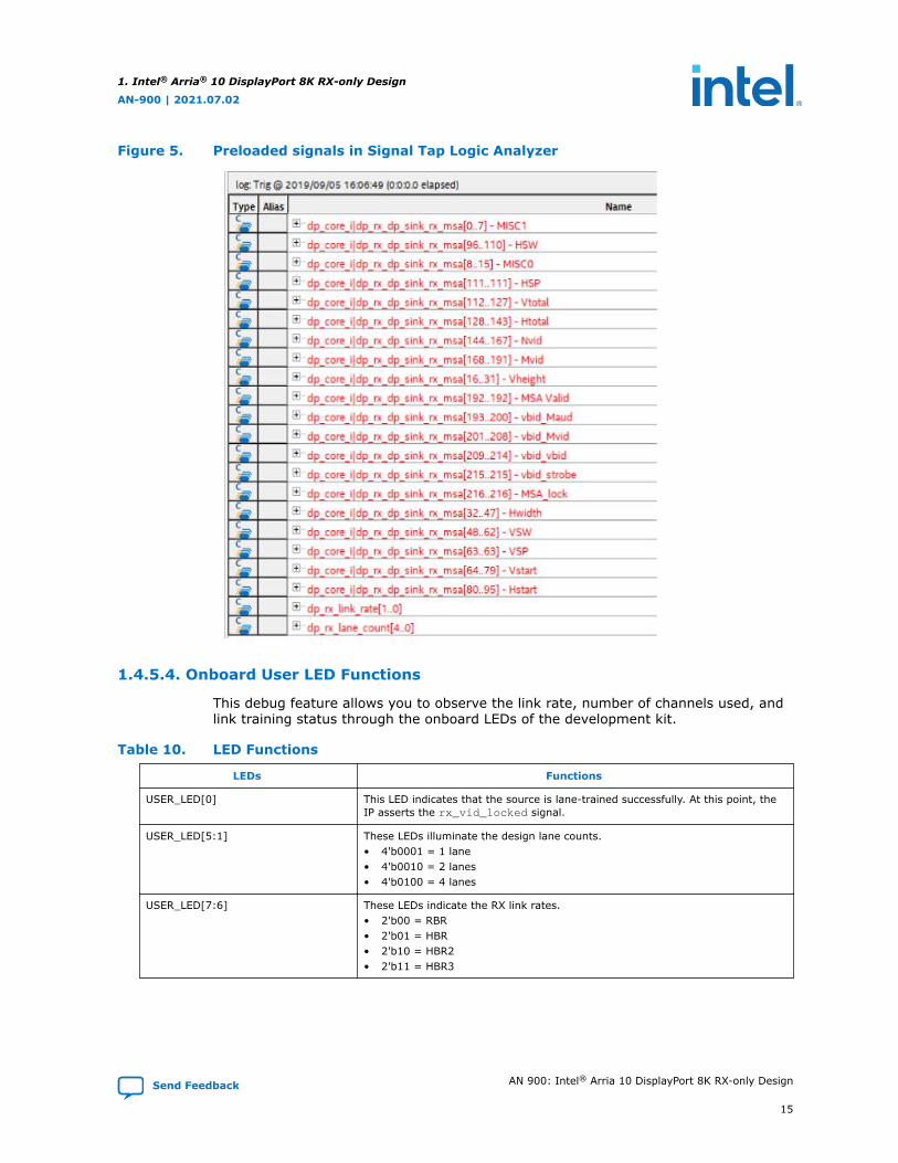
Figure 5. Preloaded signals in Signal Tap Logic Analyzer
1.4.5.4. Onboard User LED Functions
This debug feature allows you to observe the link rate, number of channels used, andlink training status through the onboard LEDs of the development kit.
Table 10. LED Functions
LEDs Functions
USER_LED[0] This LED indicates that the source is lane-trained successfully. At this point, theIP asserts the rx_vid_locked signal.
USER_LED[5:1] These LEDs illuminate the design lane counts.• 4'b0001 = 1 lane• 4'b0010 = 2 lanes• 4'b0100 = 4 lanes
USER_LED[7:6] These LEDs indicate the RX link rates.• 2'b00 = RBR• 2'b01 = HBR• 2'b10 = HBR2• 2'b11 = HBR3
1. Intel® Arria® 10 DisplayPort 8K RX-only Design
AN-900 | 2021.07.02
Send Feedback AN 900: Intel® Arria 10 DisplayPort 8K RX-only Design
15

1.5. Creating the RX-only Design
You can create the DisplayPort RX-only design by making certain software andhardware modifications to the already provided DisplayPort SST parallel loopback withPCR design example.The steps below align with Quartus 19.2 release. For newerQuartus release, additional steps to create RX-only design may be needed.
1.5.1. Generating the Design
Before you make the modifications, first you need to generate the DisplayPort SSTParallel Loopback design example in the Intel Quartus Prime Pro Edition software.
1. Instantiate the DisplayPort Intel FPGA IP and specify the parameters.
Table 11. DisplayPort SST Parallel Loopback Parameters
Parameters Value Description
Maximum video output color depth (TX) 16 bpc This design supports GPU and monitors up to amaximum of 16 bit-per-color depth. However,the design depends highly on the GPU'scapability to transmit the color depth.Note: Intel source devices are capable of
transmitting 8Kp30 with 8 bpc settings.
Maximum link rate 8.1 Gbps The bandwidth requirement for 8Kp30 and 8bpc video stream through serial link:• Active video resolution = 7680 × 4320
pixels per frame• Total resolution (including reduced blanking)
= 7760 × 4381 pixels per frame• Refresh rate = 30 Hz or 30 frames per
second• Bits per pixel = 8 bpc × 3 colors = 24 bits
per pixel• Total bandwidth = (7760 × 4381) pixels per
frame × 30 frames per second × 24 bits perpixel = 24.477 Gbps
With 8B/10B encoding scheme, the actualbandwidth required = 24.477 Gbps × 10/8 =30.59 Gbps.With 4 lanes at 8.1 Gbps, the aggregatedbandwidth of 32.4 Gbps is sufficient to supportthe 8K video stream at 30 Hz refresh rate.
Maximum lane count 4
Symbol output mode (Source) Quad Symbol mode affects the transceiver parallelbus width and the DisplayPort IP clockfrequency. The DisplayPort IP synchronizes withthe transceiver parallel clock. The parallel clockfrequency is link rate/transceiver parallel buswidth.Frequency for HBR3 (8.1 Gbps) is 8100/40 or202.5 MHz for quad (40 bits) mode.
Symbol input mode (Sink)
Pixel input mode (Source) Quad Pixel mode affects the video clock frequencyand video port width of the IP core.For 8Kp30 video stream, the bandwidthrequirement is 7760 (H-total) × 4381 (V-total)× 30 frames per second = 1019896800 pixels
Pixel output mode (Sink)
continued...
1. Intel® Arria® 10 DisplayPort 8K RX-only Design
AN-900 | 2021.07.02
AN 900: Intel® Arria 10 DisplayPort 8K RX-only Design Send Feedback
16

Parameters Value Description
per second. Because of the high bandwidthrequirement, the design requires quad pixelmode for timing closure.• Single (1 pixel/clock): 1019.89 MHz• Dual (2 pixels/clock) 509.95 MHz• Quad (4 pixels/clock) 254.97 MHzNote: This design uses 300 MHz for the video
clock generated from PLL.
Support analog reconfiguration On Enable analog reconfiguration interface. Usedto reconfigure vod and pre-emphasis value.
Enable AUX debug stream On Enable AUX source traffic output to the Avalonstreaming port
DisplayPort SST Parallel Loopback With PCR On Enable Pixel Clock Recovery in the design.
Note: The table above is an example of IP setting. However, it is recommended togenerate base example design with required IP setting (BPC, symbol perclock, pixel per clock, number of channels, link rate) and then proceed withthe design modification. Changing the IP settings at the later stage maycause design conflict if not done properly.
2. Click Generate Example Design with Intel Arria 10 GX FPGA Development Kit asa target board.
1.5.2. Removing Irrelevant Blocks
The generated DisplayPort SST Parallel Loopback design example consists of TX andRX components. Modify the generated design example by removing the irrelevantblocks from the top-level design and from the dp_core.qsys file.
Remove the TX sub-system and TX PHY top components, and the Pixel Clock Recovery(PCR) and Transceiver Arbiter blocks (in gray), as shown in the diagram below. Theseblocks are not needed for the RX-only design.
1. Intel® Arria® 10 DisplayPort 8K RX-only Design
AN-900 | 2021.07.02
Send Feedback AN 900: Intel® Arria 10 DisplayPort 8K RX-only Design
17

Figure 6. Components Required for the DisplayPort RX-only Design
Top
DebugFIFO
EDIDRAM
Pixel ClockRecovery
(PCR)
TransceiverArbiter
IOPLL
Control/Status
Serial Data
Parallel Data
Avalon-MM
RX only component
Removed component
Audio Data
Video Data Video Data
TX PHY Top
TX PLL
TransceiverPHY ResetController
TXReconfiguration
Management
DisplayPort RXCore
Avalon-MMInterconnect
Avalon-MMInterconnect
DisplayPort TXCore
DebugFIFO
PIO
CPU Sub-system
PIO
TX Sub-system (Qsys)
Core System (Qsys)
RX Sub-system (Qsys)
VideoPattern
Generator
TransceiverNative PHY
TransceiverPHY ResetController
TransceiverNative PHY
RX PHY Top
RXReconfiguration
Management
1.5.2.1. Removing Irrelevant Block in Top Level Example Design a10_dp_demo.vFile
Follow the steps below to remove irrelevant blocks in the top level file:
1. Module a10_dp_demo IO port modifications:
• Remove Transceiver Data TX outputs - fmca_dp_c2m_p signals.
• Remove other TX signals (TX CAD, TX HPD and TX Aux signals).
2. DisplayPort core Qsys system dp_core instantiation modifications:
• Remove DisplayPort Source Sub-system.
3. Remove tx_phy_top module instantiation.
4. Remove a10_reconfig_arbiter module instantiation.
5. Remove Bitec_clkrec module instantiation.
1.5.2.2. Removing Irrelevant Block in Platform Designer
Follow the steps below to remove irrelevant blocks in Platform Designer:
1. From Quartus Project Navigator, double click to open dp_core system.
2. Remove dp_tx sub-system.
3. Remove unused TX components dp_tx_clk_16 bridge anddp_tx_reset_bridge.
1. Intel® Arria® 10 DisplayPort 8K RX-only Design
AN-900 | 2021.07.02
AN 900: Intel® Arria 10 DisplayPort 8K RX-only Design Send Feedback
18

Note: Before generating HDL, save the changes in Platform Designer, Sync System Info andValidate System Integrity to ensure no errors were introduced.
1.5.3. Making a Direct Connection to the RX Transceiver Block
The existing dynamic DisplayPort parallel SST loopback with PCR design example usesthe Transceiver Arbiter block to share between an RX and TX Native PHY transceiverwithin the same channel. As the RX-only design only requires the RX transceiver, youneed to remove the Transceiver Arbiter and make a direct connection to the RXtransceiver.
1. Before you make the connection, in the Platform Designer turn on the ShareReconfiguration Interface parameter in the Transceiver Native PHY block toallow for single Avalon memory-mapped slave interface for dynamicreconfiguration of all channels.
2. Update the width of the transceiver signals as shown below in the design top-leveland the rx_phy_top.v files.
Table 12. RX Transceiver Signals
Signal Direction Width (Bit)
gxb_rx_rcfg_write Input 1
gxb_rx_rcfg_read Input 1
gxb_rx_rcfg_address Input 12
gxb_rx_rcfg_writedata Input 32
gxb_rx_rcfg_readdata Output 32
gxb_rx_rcfg_waitrequest Output 1
gxb_rx_rcfg_cal_busy Output 1
3. Make a direct connection from the RX Reconfiguration Management block to theRX Transceiver Native PHY block in the rx_phy_top.v file as shown in thediagram below.
1. Intel® Arria® 10 DisplayPort 8K RX-only Design
AN-900 | 2021.07.02
Send Feedback AN 900: Intel® Arria 10 DisplayPort 8K RX-only Design
19

Figure 7. Bitec Reconfig and RX Transceiver Block Connection
rx_phy_top
RX Transceiver Reconfig Interface
RX Transceiver Interface
rx_rcfg_write
rx_rcfg_read
rx_rcfg_address
rx_rcfg_writedata
rx_rcfg_readdata
rx_rcfg_waitrequest
rx_rcfg_cal_busy
gxb_rx_rcfg_write
gxb_rx_rcfg_read
gxb_rx_rcfg_address
gxb_rx_rcfg_writedata
gxb_rx_rcfg_readdata
gxb_rx_rcfg_waitrequest
gxb_rx_rcfg_cal_busy
4. Remove the following Transceiver Reconfig Group assignments from theIntel Quartus Prime Settings File (.qsf).
• - set_instance_assignment -name XCVR_RECONFIG_GROUP 1 -tofmca_dp_m2c_p[0] -entity a10_dp_demo
• - set_instance_assignment -name XCVR_RECONFIG_GROUP 2 -tofmca_dp_m2c_p[1] -entity a10_dp_demo
• - set_instance_assignment -name XCVR_RECONFIG_GROUP 3 -tofmca_dp_m2c_p[2] -entity a10_dp_demo
• - set_instance_assignment -name XCVR_RECONFIG_GROUP 4 -tofmca_dp_m2c_p[3] -entity a10_dp_demo
1. Intel® Arria® 10 DisplayPort 8K RX-only Design
AN-900 | 2021.07.02
AN 900: Intel® Arria 10 DisplayPort 8K RX-only Design Send Feedback
20
1.5.4. Selecting the Bitec FMC Daughter Card Revision
Make sure that the Bitec daughter card revision is updated accordingly.
To update the Bitec daughter card revision, edit the top-level project file and in theconfig.h software file. This design uses Bitec daughter card revision 11 to supportHBR3 data rate.
localparam BITEC_DP_CARD_REV = 2;
// 0 = Bitec FMC DP card rev.4 - 8,
// 1 = rev.9 - 10
// 2 = rev.11
1.5.5. Modifying the Software
After removing the irrelevant blocks, reconnecting the remaining blocks, and selectingthe Bitec FMC daughter card revision, modify the software.
1. First, modify the software's config.h file. Navigate to the design example folderand change the values of the following parameter settings in the file.
Table 13. Config.h Parameter Settings
Parameter Value Description
BITEC_AUX_DEBUG 0 Set to 1 to enable AUX channel trafficmonitoring.
BITEC_STATUS_DEBUG 1 Set to 1 to enable MSA and link statusmonitoring.
DP_SUPPORT_RX 1 Set to 1 if the DisplayPort supports RX.
BITEC_RX_GPUMODE 1 Set to 1 to enable sink GPU mode.
BITEC_RX_CAPAB_MST 0 Set to 1 to enable MST support.
BITEC_RX_FAST_LT_SUPPORT 0 Set to 1 to enable Fast Link Training support.
BITEC_RX_LQA_SUPPORT 0 Set to 1 to enable Link Quality Analysissupport.
BITEC_EDID_800X600_AUDIO 0 Set to 1 to use an EDID with maximumresolution of 800 x 600
BITEC_DP_0_AV_RX_CONTROL_BITEC_CFG_RX_SUPPORT_MST
0 Set to 1 to enable MST support
DP_SUPPORT_TX 0 Set to 1 if DisplayPort supports TX
BITEC_TX_CAPAB_MST 0 Set to 1 to enable MST support
TX_VIDEO_IM_ENABLE 0 Set to 1 to enable TX Video IM interface
DP_SUPPORT_EDID_PASSTHRU 0 Set to 1 to enable EDID passthrough from sinkto source.
continued...
1. Intel® Arria® 10 DisplayPort 8K RX-only Design
AN-900 | 2021.07.02
Send Feedback AN 900: Intel® Arria 10 DisplayPort 8K RX-only Design
21

Parameter Value Description
BITEC_DP_CARD_REV 0, 1 or 2 • Set to 0 = Bitec FMC DisplayPort daughtercard revision 4 – 8 (without ParadetechRetimer)
• Set to 1 = Bitec FMC DisplayPort daughtercard revision 9 and 10 (with ParadetechRetimer)
• Set to 2 = Bitec FMC DisplayPort daughtercard revision 11 (with Megachip Retimer)
MST_RX_STREAMS 0 RX MST number of streams
MST_TX_STREAMS 0 TX MST number of streams
PSG_8K_EDID 1 Set to 1 is sink supports 8K video.
2. Next, open the main.c file located in the software/dp_demo folder, and removeany TX-related components, such as the following:
- #include “tx_utils.h”
- bitec_dptx_init();
- bitec_dp_dump_source_msa(btc_dptx_baseaddr(0));
- bitec_dp_dump_source_config(btc_dptx_baseaddr(0));
Note: Remove the tx_utils.c and tx_utils.h files from the software folder toavoid potential software build errors.
3. Next, for debugging purposes, modify the debug.c file located in the software/dp_demo folder. Open the debug.c file and remove the voidbitec_dp_dump_source_msa() and voidbitec_dp_dump_source_config() functions.
4. After modifying the software, rebuild the software as instructed in Regeneratingand Downloading ELF File on page 9.
5. Finally, compile the project as described in Compiling the Design on page 8.
1.6. Document Revision History for AN 900: Intel Arria 10DisplayPort 8K RX-only Design
DocumentVersion
Changes
2021.07.02 • Added Bitec FMC daughter card revision 8 to Hardware and Software Requirements.• Added the step to extract the file inCompiling the Design.• Edited the step in Regenerating and Downloading ELF File.• Pointed Reset Button in Figure: Intel Arria 10 Development Kit Setup.• Changed from output to input in Design Debug Features.• Added the steps in Creating the RX-only Design.• Added subtopic Removing Irrelevant Block in Top Level Example Design a10_dp_demo.v File and
Removing Irrelevant Block in Platform Designer in section Removing Irrelevant Blocks.• Edited the steps and changed the Figure:Bitec Reconfig and RX Transceiver Block Connection in
Making a Direct Connection to the RX Transceiver Block.
2019.12.16 Initial release.
1. Intel® Arria® 10 DisplayPort 8K RX-only Design
AN-900 | 2021.07.02
AN 900: Intel® Arria 10 DisplayPort 8K RX-only Design Send Feedback
22


