Adv. Eng. Tec. Appl. 3, No. 2, 13-19 (2014) 13 Advanced Engineering Technology and Application An International Journal http://dx.doi.org/10.12785/aeta/paper An Area Efficient Approach: Comparative Analysis of Multiplier Circuits Amit Grover 1,∗ , Jyoti Gupta 1 , Keshav Kumar 1 , Neeti Grover 2 and Sumer Singh 3 1 Department of Electronics & Communication Engineering, S.B.S State Technical Campus Ferozepur, Punjab, India 2 Department of Applied Sciences and Humanities, S.B.S State Technical Campus Ferozepur, Punjab, India 3 Department of Electronics & Communication Engineering, Government Polytechnic College, Ferozepur, Punjab, India Received: 5 Jan. 2014, Revised: 3 Mar. 2014, Accepted: 5 Mar. 2014 Published online: 1 May 2014 Abstract: Improvements in the performance of integrated circuits include scaling of transistor size and reduction of operating voltage. Smaller area and power dissipation have also taken care of for fabrication of high performance. Optimizing the power consumption, speed, area and delay of the multiplier are a major issue. In this article, the best solution to this problem is determined. As we know, Adders and Multipliers are key components of many high performance systems. By designing different multipliers, implementing their components is better to choose an option between CSL, DPL & CPL adders in fabricating different systems. This article focuses on the comparison between two algorithms for multiplication, Array and Wallace Tree. The implementation of these algorithms is performed by designing (4 × 4and8 × 8) bit multiplier blocks in 0.18μ C MOS technology using EDA Tanner v.13 (evaluation version) framework tools. Furthermore, the 8-bit multipliers on GDI adder cells are compared using EDA Tanner. Multiplier design in this article provides the low power requirement and presents an area efficient approach. Moreover, number of transistors is also less as compared to CMOS for any design. Keywords: CSL, DPL, CPL, GDI 1 Introduction Digital multiplication is one of the most basic functions in a wide range of algorithms. Being the slowest element in the system, the performance of the system is determined by the performance of the multiplier block. Today multiplication is not only implemented with a sequence of addition, subtraction and shift operations. Many speed effective and power effective algorithms have been evolved depending upon the use in an application. From a delay perspective, algorithms place two constraints on multiplication: latency and throughput. Latency is the real delay of computing a function, a measure of how long after the inputs to a device are stable, is the final result available on the outputs. Throughput is a measure of how many multiplications can be performed in a given amount of time. Multiplier [1] in addition to a high delay block is also a major source of power dissipation, many algorithm are designed with the help of digital multiplication. So it is of great interest to identify and apply algorithms which has less delay as well as less power consumption of the multiplier i.e. which has smaller power delay product and fast processing. Bulks of both NMOS and PMOS are connected to N or P (respectively), so it can be arbitrarily biased at contrast with a CMOS inverter. 2 Preliminaries A. Logic Equations for the Proposed Full Adders The equations presented below can be stated as follows: Sum = A ⊕ B ⊕ Cin (1) Sum = A ⊕ B ⊕ Cin (2) Sum = C in(A ⊕ B)+ Cin(A ⊕B) (3) Cout = A.(A ⊕ B + C in(A ⊕ B)) (4) ∗ Corresponding author e-mail: amitgrover [email protected]c ⃝ 2014 NSP Natural Sciences Publishing Cor.
Transcript
Adv. Eng. Tec. Appl. 3, No. 2, 13-19 (2014) 13
Advanced Engineering Technology and ApplicationAn International Journal
http://dx.doi.org/10.12785/aeta/paper
An Area Efficient Approach: Comparative Analysis ofMultiplier Circuits
Amit Grover 1,∗, Jyoti Gupta1, Keshav Kumar 1, Neeti Grover2 and Sumer Singh3
1 Department of Electronics & Communication Engineering, S.B.S State Technical Campus Ferozepur, Punjab, India2 Department of Applied Sciences and Humanities, S.B.S State Technical Campus Ferozepur, Punjab, India3 Department of Electronics & Communication Engineering, Government Polytechnic College, Ferozepur, Punjab, India
Received: 5 Jan. 2014, Revised: 3 Mar. 2014, Accepted: 5 Mar. 2014Published online: 1 May 2014
Abstract: Improvements in the performance of integrated circuits include scaling of transistor size and reduction of operating voltage.Smaller area and power dissipation have also taken care of for fabrication of high performance. Optimizing the power consumption,speed, area and delay of the multiplier are a major issue. In this article, the best solution to this problem is determined. As we know,Adders and Multipliers are key components of many high performance systems. By designing different multipliers, implementing theircomponents is better to choose an option between CSL, DPL & CPL adders in fabricating different systems. This article focuses on thecomparison between two algorithms for multiplication, Array and Wallace Tree. The implementation of these algorithms is performedby designing (4×4and8×8) bit multiplier blocks in 0.18µ C MOS technology using EDA Tanner v.13 (evaluation version) frameworktools. Furthermore, the 8-bit multipliers on GDI adder cells are compared using EDA Tanner. Multiplier design in this article providesthe low power requirement and presents an area efficient approach. Moreover, number of transistors is also less as compared to CMOSfor any design.
Keywords: CSL, DPL, CPL, GDI
1 Introduction
Digital multiplication is one of the most basic functions ina wide range of algorithms. Being the slowest element inthe system, the performance of the system is determinedby the performance of the multiplier block. Todaymultiplication is not only implemented with a sequence ofaddition, subtraction and shift operations. Many speedeffective and power effective algorithms have beenevolved depending upon the use in an application. From adelay perspective, algorithms place two constraints onmultiplication: latency and throughput. Latency is the realdelay of computing a function, a measure of how longafter the inputs to a device are stable, is the final resultavailable on the outputs. Throughput is a measure of howmany multiplications can be performed in a given amountof time. Multiplier [1] in addition to a high delay block isalso a major source of power dissipation, many algorithmare designed with the help of digital multiplication. So itis of great interest to identify and apply algorithms whichhas less delay as well as less power consumption of the
multiplier i.e. which has smaller power delay product andfast processing.
Bulks of both NMOS and PMOS are connected to N orP (respectively), so it can be arbitrarily biased at contrastwith a CMOS inverter.
2 Preliminaries
A. Logic Equations for the Proposed Full AddersThe equations presented below can be stated as
14 A. Grover et. al. : An Area Efficient Approach: Comparative Analysis of Multiplier Circuits
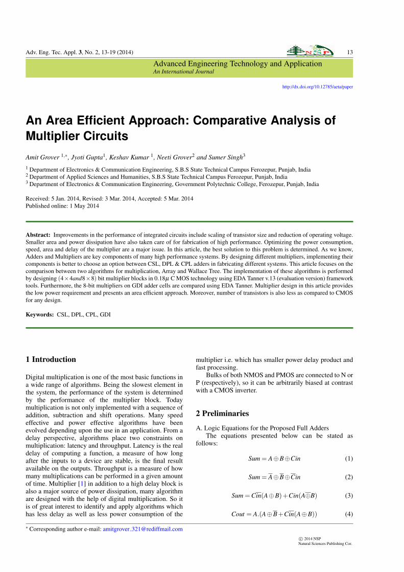
Fig. 1: GDI basic cell [2]
Table 1: Various logic functions of GDI cell for different cell fordifferent input configurations
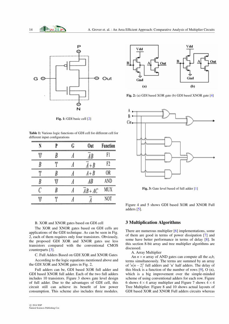
B. XOR and XNOR gates based on GDI cellThe XOR and XNOR gates based on GDI cells are
applications of the GDI technique. As can be seen in Fig.2, each of them requires only four transistors. Obviously,the proposed GDI XOR and XNOR gates use lesstransistors compared with the conventional CMOScounterparts [3].
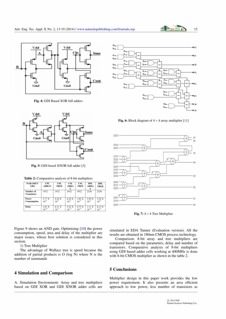
C. Full Adders Based on GDI XOR and XNOR GatesAccording to the logic equations mentioned above and
the GDI XOR and XNOR gates in Fig. 2,Full adders can be, GDI based XOR full adder and
GDI based XNOR full adder. Each of the two full addersincludes 10 transistors. Figure 3 shows gate level designof full adder. Due to the advantages of GDI cell, thiscircuit still can achieve its benefit of low powerconsumption. This scheme also includes three modules.
Fig. 2: (a) GDI based XOR gate (b) GDI based XNOR gate [4]
Fig. 3: Gate level based of full adder [1]
Figure 4 and 5 shows GDI based XOR and XNOR Fulladders [5].
3 Multiplication Algorithms
There are numerous multiplier [6] implementations, someof them are good in terms of power dissipation [7] andsome have better performance in terms of delay [8]. Inthis section 8-bit array and tree multiplier algorithms arediscussed.
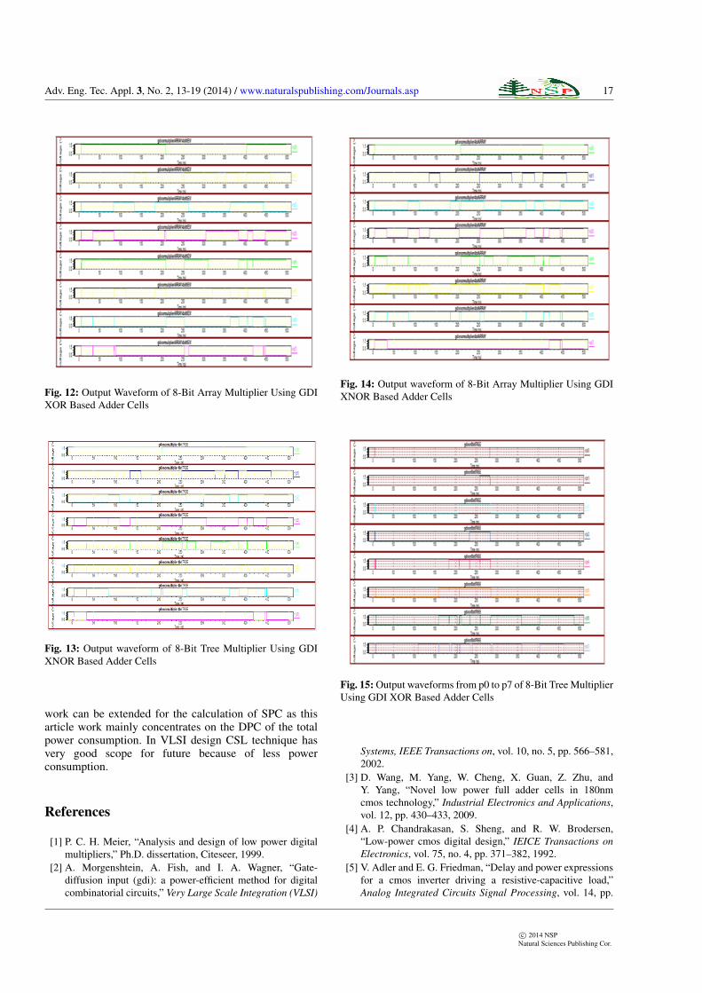
A. Array MultiplierAn n×n array of AND gates can compute all the aibi
terms simultaneously. The terms are summed by an arrayof ′n[n− 2]′ full adders and ’n’ half adders. The delay ofthis block is a function of the number of rows [9], O (n),which is a big improvement over the simple-mindedscheme of using conventional adders for each row. Figure6 shows 4× 4 array multiplier and Figure 7 shows 4× 4Tree Multiplier. Figure 8 and 10 shows actual layouts ofGDI based XOR and XNOR Full adders circuits whereas
Table 2: Comparative analysis of 8-bit multipliers
Figure 9 shows an AND gate. Optimizing [10] the powerconsumption, speed, area and delay of the multiplier aremajor issues, whose best solution is considered in thissection.
1) Tree MultiplierThe advantage of Wallace tree is speed because the
addition of partial products is O (log N) where N is thenumber of summands
4 Simulation and Comparison
A. Simulation Environment: Array and tree multipliersbased on GDI XOR and GDI XNOR adder cells are
Fig. 6: Block diagram of 4×4 array multiplier [11]
Fig. 7: 4×4 Tree Multiplier
simulated in EDA Tanner (Evaluation version). All theresults are obtained in 180nm CMOS process technology.
Comparison: 8-bit array and tree multipliers arecompared based on the parameters, delay and number oftransistors. Comparative analysis of 8-bit multipliersusing GDI based adder cells working at 400MHz is donewith 8-bit CMOS multiplier as shown in the table 2.
5 Conclusions
Multiplier design in this paper work provides the lowpower requirement. It also presents an area efficientapproach to low power, less number of transistors as
c⃝ 2014 NSPNatural Sciences Publishing Cor.
16 A. Grover et. al. : An Area Efficient Approach: Comparative Analysis of Multiplier Circuits
Fig. 8: GDI Based XOR full adder
Fig. 9: Schematic of AND Gate
compared to CMOS and DCVS for any design. 8-bitmultipliers were designed in Tanner (Evaluation version)tool using 180nm and analysis of dynamic powerdissipation, delay and area was done. The results in table2 are at frequency 400MHz and load capacitance is 1pF.Channel length for both NMOS & PMOS is 180nm andwidth is 1790nm for PMOS & 699nm for NMOStransistor.
Fig. 10: GDI Based XNOR full adders
Fig. 11: Output waveform of 8-Bit Tree Multiplier Using GDIXOR Based Adder Cells
6 Future scope
As a future scope of the work, Power of the circuit can befurther reduced if requirement of buffers in the circuit isavoided. Also, this technique can be compounded withother methods used such as using sleep transistors, dualthreshold CMOS, dynamic threshold CMOS. This articlework is based on combinational circuit design.Techniques can also be applied to sequential circuits. The
Fig. 12: Output Waveform of 8-Bit Array Multiplier Using GDIXOR Based Adder Cells
Fig. 13: Output waveform of 8-Bit Tree Multiplier Using GDIXNOR Based Adder Cells
work can be extended for the calculation of SPC as thisarticle work mainly concentrates on the DPC of the totalpower consumption. In VLSI design CSL technique hasvery good scope for future because of less powerconsumption.
References
[1] P. C. H. Meier, “Analysis and design of low power digitalmultipliers,” Ph.D. dissertation, Citeseer, 1999.
[2] A. Morgenshtein, A. Fish, and I. A. Wagner, “Gate-diffusion input (gdi): a power-efficient method for digitalcombinatorial circuits,” Very Large Scale Integration (VLSI)
Fig. 14: Output waveform of 8-Bit Array Multiplier Using GDIXNOR Based Adder Cells
Fig. 15: Output waveforms from p0 to p7 of 8-Bit Tree MultiplierUsing GDI XOR Based Adder Cells
Systems, IEEE Transactions on, vol. 10, no. 5, pp. 566–581,2002.
[3] D. Wang, M. Yang, W. Cheng, X. Guan, Z. Zhu, andY. Yang, “Novel low power full adder cells in 180nmcmos technology,” Industrial Electronics and Applications,vol. 12, pp. 430–433, 2009.
[4] A. P. Chandrakasan, S. Sheng, and R. W. Brodersen,“Low-power cmos digital design,” IEICE Transactions onElectronics, vol. 75, no. 4, pp. 371–382, 1992.
[5] V. Adler and E. G. Friedman, “Delay and power expressionsfor a cmos inverter driving a resistive-capacitive load,”Analog Integrated Circuits Signal Processing, vol. 14, pp.
c⃝ 2014 NSPNatural Sciences Publishing Cor.
18 A. Grover et. al. : An Area Efficient Approach: Comparative Analysis of Multiplier Circuits
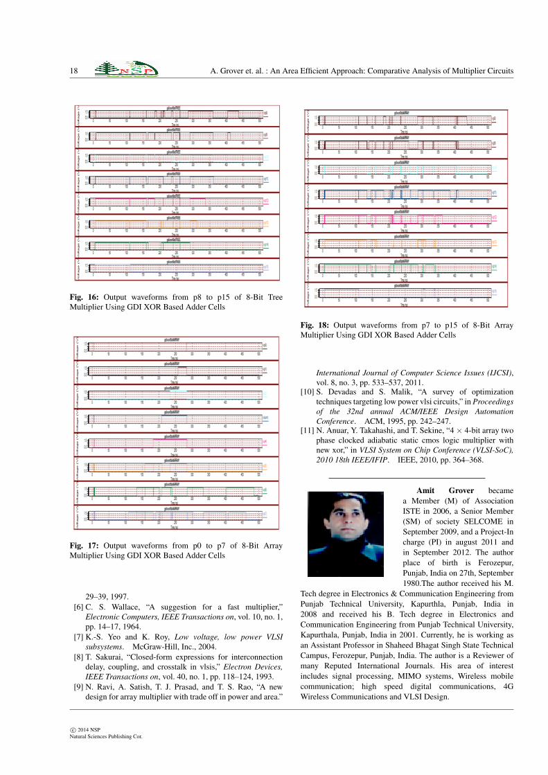
Fig. 16: Output waveforms from p8 to p15 of 8-Bit TreeMultiplier Using GDI XOR Based Adder Cells
Fig. 17: Output waveforms from p0 to p7 of 8-Bit ArrayMultiplier Using GDI XOR Based Adder Cells
29–39, 1997.[6] C. S. Wallace, “A suggestion for a fast multiplier,”
[7] K.-S. Yeo and K. Roy, Low voltage, low power VLSIsubsystems. McGraw-Hill, Inc., 2004.
[8] T. Sakurai, “Closed-form expressions for interconnectiondelay, coupling, and crosstalk in vlsis,” Electron Devices,IEEE Transactions on, vol. 40, no. 1, pp. 118–124, 1993.
[9] N. Ravi, A. Satish, T. J. Prasad, and T. S. Rao, “A newdesign for array multiplier with trade off in power and area.”
Fig. 18: Output waveforms from p7 to p15 of 8-Bit ArrayMultiplier Using GDI XOR Based Adder Cells
International Journal of Computer Science Issues (IJCSI),vol. 8, no. 3, pp. 533–537, 2011.
[10] S. Devadas and S. Malik, “A survey of optimizationtechniques targeting low power vlsi circuits,” in Proceedingsof the 32nd annual ACM/IEEE Design AutomationConference. ACM, 1995, pp. 242–247.
[11] N. Anuar, Y. Takahashi, and T. Sekine, “4 × 4-bit array twophase clocked adiabatic static cmos logic multiplier withnew xor,” in VLSI System on Chip Conference (VLSI-SoC),2010 18th IEEE/IFIP. IEEE, 2010, pp. 364–368.
Amit Grover becamea Member (M) of AssociationISTE in 2006, a Senior Member(SM) of society SELCOME inSeptember 2009, and a Project-Incharge (PI) in august 2011 andin September 2012. The authorplace of birth is Ferozepur,Punjab, India on 27th, September1980.The author received his M.
Tech degree in Electronics & Communication Engineering fromPunjab Technical University, Kapurthla, Punjab, India in2008 and received his B. Tech degree in Electronics andCommunication Engineering from Punjab Technical University,Kapurthala, Punjab, India in 2001. Currently, he is working asan Assistant Professor in Shaheed Bhagat Singh State TechnicalCampus, Ferozepur, Punjab, India. The author is a Reviewer ofmany Reputed International Journals. His area of interestincludes signal processing, MIMO systems, Wireless mobilecommunication; high speed digital communications, 4GWireless Communications and VLSI Design.
Jyoti Gupta receivedher B.Tech degree in ECEin 2012 from Baba Farid Collegeof Engineering and Technology,Affiliated to PTU, Kapurthala,Punjab. Her place of birthis Ferozepur, Punjab, India on20th April, 1990. At present shehas been doing her research work
under the guidance of Mr. Amit Grover, AssistantProfessor, Department of ECE, Shaheed Bhagat SinghState Technical Campus, Moga road, Ferozepur, India.
Keshav Kumar is pursuinghis Master of Technologyin the area of Electronicsand Communication Engineeringunder the supervision of Mr.Amit Grover, Assistant Professor,Department of Electronics& Communication Engineering,Shaheed Bhagat Singh StateTechnical Campus (Established
by Govt. of Punjab) Moga road, Ferozepur, Punjab,India. The author place of birth is Banmankhi, Distt.Purnea, Bihar India on 15th, April 1989. KeshavKumar received his B. Tech degree in the area ofElectronics & Communication Engineering in 2011 FromBaba Hira Singh Bhattal Institute of Engineering &Technology (Established by Govt. of Punjab) Lehragaga,Distt-Sangrur, Punjab, India.
Neeti Grover receivedher master degree in AppliedSciences from Guru Nanak DevUniversity, Amritsar, and Punjab,India in 2007 and receivedher Bachelors degree from GuruNanak Dev University, Amritsar,Punjab, India in 2004. Her placeof birth is Jallandhar, Punjab,
India on 29th, December 1983. Currently, she is workingas an Assistant Professor in the department of AppliedSciences and Humanities in Shaheed Bhagat Singh StateTechnical Campus (Poly Wing), Ferozpur, Punjab, India.
Sumer Singh the authorplace of birth is Ferozepur,Punjab, India on 15th, August1985. The author receivedhis M.Tech degree in Electronicsand Communication Engineeringfrom Punjab TechnicalUniversity, Kapurthla, Punjab,India in 2013 and received hisB.Tech degree in Electronics and
Communication Engineering from Punjab TechnicalUniversity, Kapurthala, Punjab, India in 2010. Currently,he is working as a Lecturer in Department of Electronics& Communication Engineering, Government PolytechnicCollege, Ferozepur, Punjab India. His area of interestincludes Wireless Communication Network, Mobile AdHoc Network, Wireless Sensor Network and VLSIDesign.


![Multidimensional cyclic graph approach: Representing a ... · Efficient cube approaches, such as the multidimensional direct acyclic graph (MDAG) approach [20], the Dwarf approach](https://static.documents.pub/doc/80x56/5fbc402eed62fa0b8806d8da/multidimensional-cyclic-graph-approach-representing-a-eficient-cube-approaches.jpg)


