How to Implement the Freescale MPL115A Digital Barometerby John Young
INTRODUCTION
MPL115A is a simple barometer with digital output and high performance targeting low cost commercial applications The device employs a MEMS PRT pressure sensor with a conditioning IC to provide accurate pressure data The sensor output is accurate to plusmn1 kPa over the 50 kPa to 115 kPa pressure range An integrated ADC provides digitized temperature and pressure sensor outputs via an I2C or SPI bus The partrsquos operating voltage is from 2375 V to 55 V The part is available as either the MPL115A1 (SPI) or MPL115A2 (I2C) part The customer can order the device in either bus protocol depending on which is more convenient for their end application
Calibration data is housed in on-board ROM This data is used by a host microcontroller to apply a compensation algorithm to the raw ADC data from the pressure sensor and may be accessed at any time The Calibration data is stored as a series of coefficients that are applied to the raw data to compensate for temperature and pressure variation in the raw output
The following application note will describe the SPI and I2C protocol needed to communicate to the digital pressure sensor Following communication and extraction of the stored coefficients raw data from the sensorrsquos PRT can be compensated on the host microcontroller for pressure and temperature The application note details this process and the end result of the calculation is Compensated Pressure
Updates to this Application Note
This application note has been updated to reflect changes in the pressure compensation algorithm - the 2nd order coefficients have now been removed This modifies the compensated Pressure equation to be simpler than the previous version Both are detailed so a comparsion can be made Particular details have also migrated to the datasheet for MPL115A1 and MPL115A2 to expand on content in those documents
Sample Boards
Freescale has two sample eval boards available in either SPI or I2C MPL115A device variations KITMPL115A1SPI or KITMPL115A2I2C These are simple PCB boards with sensor parts associated pullup resistors and decoupling capacitors soldered onboard for customer evaluation This provides a quick sample tool to run evaluations of the small device given its LGA footprint
copy Freescale Semiconductor Inc 2008 2009 2011 2012 All rights reserved
The MPL115A is an absolute pressure sensor with digital output for low cost applications A miniature 5 x 3 x 12 mm LGA package ideally suits it for portable electronics and space constrained applications Low current consumptions of 5 A during Active mode and 1 A during Shutdown (Sleep) mode target battery and other low-power applications A wide operating temperature range from -40degC to +105degC fits demanding environmental requirements
MPL115A employs a MEMS pressure sensor with a conditioning IC to provide accurate pressure measurement from 50 to 115 kPa An integrated ADC provides digitized temperature and pressure sensor outputs via an I2C or SPI port Calibration Data is stored in internal ROM Utilizing raw sensor output the host microcontroller executes a compensation algorithm to render Compensated Absolute Pressure with 1 kPa accuracy
The MPL115A pressure sensorrsquos small form factor low power capability precision and digital output optimize it for barometric measurement applications
VDD
VDD1VDD1
1
AB
SW1
AB
SW1
3 2 1
C3
01UF
C3
01UF
GND1GND1
1
C1
10UF
C1
10UF
U1
MPL115A1
U1
MPL115A1
GND
3
DOUT 6DIN7
VDD
1
CS 5SCLK 8CAP2SHDN4
J4J4
1234
C2
10UF
C2
10UF
SHDN
VDD
VDDVDD
C3
01UF
C3
01UF
R1470KR1470K
AB
SW1
AB
SW1
3 2 1
U1
MPL115A2
U1
MPL115A2
GND
3
DOUT 67
VDD
1
SCL 8CAP2
VDD1VDD1
1
J1
HDR_1X2
J1
HDR_1X2
12
C1
10UF
C1
10UF
R3470KR3470K
GND1GND1
1
R2470KR2470K
C2
10UF
C2
10UF
4SHDN RST
5
SDA
AN3785
SensorsFreescale Semiconductor 2
1 Mechanical and Electrical Specifications
11 Maximum RatingsVoltage (with respect to GND unless otherwise noted)
VDD -03 V to +55 V
SHDN SCLK CS DIN DOUT -03 V to VDD+03 V
Operating Temperature Range -40degC to +105degC
Storage Temperature Range-40degC to +125degC
Overpressure 1000 kPa
12 Operating CharacteristicsVDD = 2375 V to 55 V TA = -40degC to +105degC unless otherwise noted Typical values are at VDD = 33 V TA = +25degC
Ref Parameters Symbol Conditions Min Typ Max Units
1 Operating Supply Voltage VDD 2375 33 55 V
2 Supply Current IDD Shutdown (SHDN = GND) mdash mdash 1 A
Standby mdash 35 10 A
Average ndash at one measurement per second mdash 5 6 A
Pressure Sensor
3 Range 50 mdash 115 kPa
4 Resolution mdash 015 mdash kPa
5 Accuracy -20ordmC to 85ordmC mdash mdash plusmn1 kPa
6 Power Supply Rejection Typical operating circuit at DC 01 mdash kPaV
100 mV p-p 217 Hz square wave plus 100 mV pseudo random noise with 10 MHz bandwidth
01 mdash kPa
7 Conversion Time(Start Pressure and Temperature Conversion)
tc Time between start convert command and data available in the Pressure and Temperature registers
mdash 16 3 ms
8 Wakeup Time tw Time between leaving Shutdown mode (SHDN goes high) and communicating with the device to issue a command or read data
mdash 3 5 ms
I2C IO Stages SCL SDA
9 SCL Clock Frequency fSCL mdash mdash 400 kHz
10 Low Level Input Voltage VIL mdash mdash 03VDD V
11 High Level Input Voltage VIH 07VDD mdash mdash V
I2C Outputs SDA
12 Data Setup Time tSU Setup time from command receipt to ready to transmit
0 mdash 04 s
I2C Addressing
MPL115A2 uses 7-bit addressing does not acknowledge the general call address 0000000 Slave address has been set to 0x60 or 1100000
AN3785
SensorsFreescale Semiconductor 3
13 Pin Connections SPITop View
Figure 3 Pin Connections SPI
14 Pin Connections I2CTop View
Figure 4 Pin Connections I2C
1
DOUT
DIN
VDD
CAP
SHDN
GND
CS
SCLK
2
3
4
8
7
6
5
1
NC
SDA
VDD
CAP
SHDN
GND
RST
SCL
2
3
4
8
7
6
5
AN3785
SensorsFreescale Semiconductor 4
2 Overview of FunctionsOperation
Figure 5 Sequence Flow Chart
The MPL115A interfaces to a host (or system) microcontroller in the userrsquos application All communications are via SPI or I2C A typical usage sequence is as follows
Initial Power-up
All circuit elements are active SPI or I2C port pins are high impedance and associated registers are cleared The device then enters standby mode
Reading Coefficient Data
The user then typically accesses the part and reads the coefficient data The main circuits within the slave device are disabled during read activity The coefficients are usually stored in the host microcontoller local memory but can be re-read at any time
It is suggested to read the coefficients once and store the values in the host microcontroller for speed It is not necessary to read this multiple times because the coefficients within a device are constant and do not change However note that the coefficients will be different from device to device and cannot be used for another part
Data Conversion
This is the first step that is performed each time a new pressure reading is required which is initiated by the host sending the CONVERT command The main system circuits are activated (wake) in response to the command and after the conversion completes the result is placed into the Pressure and Temperature ADC output registers
The conversion completes within the maximum conversion time tc of 16ms typical or 3ms max The device then enters standby mode
Compensated Pressure Reading
After the conversion has been given sufficient time to complete the host microcontroller reads the result from the ADC output registers and calculates the Compensated Pressure a barometricatmospheric pressure value which is compensated for changes in temperature and pressure sensor linearity This is done using the coefficient data from the MPL115A and the raw sampled pressure and temperature ADC output values in a compensation equation (detailed later) Note that this is an absolute pressure measurement with a vacuum as a reference
From this step the host controller may either wait and then return to the Data Conversion step to obtain the next pressure reading or it may go to the Shutdown step with the full supply voltage range
Reading coefficient data
Data conversion
Initial powerup
Compensated pressure reading
Shutdown
AN3785
SensorsFreescale Semiconductor 5
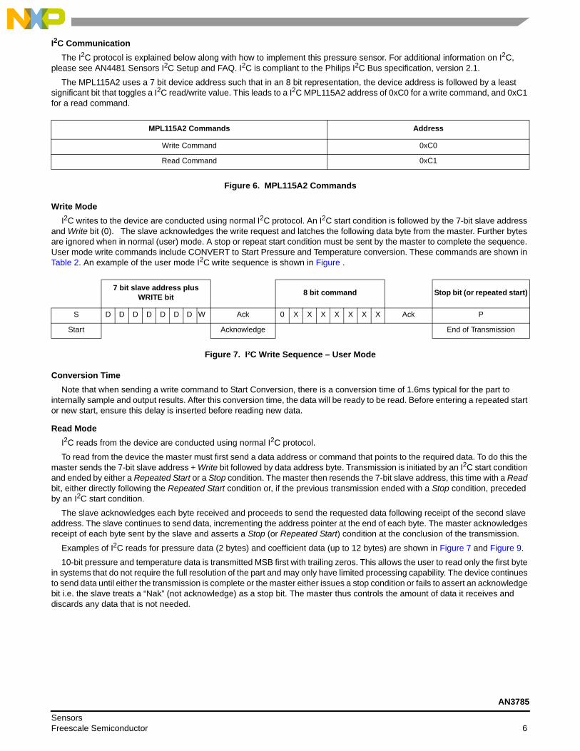
I2C Communication
The I2C protocol is explained below along with how to implement this pressure sensor For additional information on I2C please see AN4481 Sensors I2C Setup and FAQ I2C is compliant to the Philips I2C Bus specification version 21
The MPL115A2 uses a 7 bit device address such that in an 8 bit representation the device address is followed by a least significant bit that toggles a I2C readwrite value This leads to a I2C MPL115A2 address of 0xC0 for a write command and 0xC1 for a read command
Figure 6 MPL115A2 Commands
Write Mode
I2C writes to the device are conducted using normal I2C protocol An I2C start condition is followed by the 7-bit slave address and Write bit (0) The slave acknowledges the write request and latches the following data byte from the master Further bytes are ignored when in normal (user) mode A stop or repeat start condition must be sent by the master to complete the sequence User mode write commands include CONVERT to Start Pressure and Temperature conversion These commands are shown in Table 2 An example of the user mode I2C write sequence is shown in Figure
Figure 7 Isup2C Write Sequence ndash User Mode
Conversion Time
Note that when sending a write command to Start Conversion there is a conversion time of 16ms typical for the part to internally sample and output results After this conversion time the data will be ready to be read Before entering a repeated start or new start ensure this delay is inserted before reading new data
Read Mode
I2C reads from the device are conducted using normal I2C protocol
To read from the device the master must first send a data address or command that points to the required data To do this the master sends the 7-bit slave address + Write bit followed by data address byte Transmission is initiated by an I2C start condition and ended by either a Repeated Start or a Stop condition The master then resends the 7-bit slave address this time with a Read bit either directly following the Repeated Start condition or if the previous transmission ended with a Stop condition preceded by an I2C start condition
The slave acknowledges each byte received and proceeds to send the requested data following receipt of the second slave address The slave continues to send data incrementing the address pointer at the end of each byte The master acknowledges receipt of each byte sent by the slave and asserts a Stop (or Repeated Start) condition at the conclusion of the transmission
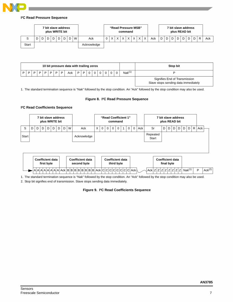
Examples of I2C reads for pressure data (2 bytes) and coefficient data (up to 12 bytes) are shown in Figure 7 and Figure 9
10-bit pressure and temperature data is transmitted MSB first with trailing zeros This allows the user to read only the first byte in systems that do not require the full resolution of the part and may only have limited processing capability The device continues to send data until either the transmission is complete or the master either issues a stop condition or fails to assert an acknowledge bit ie the slave treats a ldquoNakrdquo (not acknowledge) as a stop bit The master thus controls the amount of data it receives and discards any data that is not needed
MPL115A2 Commands Address
Write Command 0xC0
Read Command 0xC1
7 bit slave address plus WRITE bit
8 bit command Stop bit (or repeated start)
S D D D D D D D W Ack 0 X X X X X X X Ack P
Start Acknowledge End of Transmission
AN3785
SensorsFreescale Semiconductor 6
Isup2C Read Pressure Sequence
Figure 8 Isup2C Read Pressure Sequence
Isup2C Read Coefficients Sequence
Figure 9 Isup2C Read Coefficients Sequence
7 bit slave address plus WRITE bit
ldquoRead Pressure MSBrdquo command
7 bit slave address plus READ bit
S D D D D D D D W Ack 0 X X X X X X X Ack D D D D D D D R Ack
Start Acknowledge
10 bit pressure data with trailing zeros Stop bit
P P P P P P P P Ack P P 0 0 0 0 0 0 Nak(1)
1 The standard termination sequence is ldquoNakrdquo followed by the stop condition An ldquoAckrdquo followed by the stop condition may also be used
P
Signifies End of Transmission Slave stops sending data immediately
7 bit slave address plus WRITE bit
ldquoRead Coefficient 1rdquo command
7 bit slave address plus READ bit
S D D D D D D D W Ack X 0 0 0 0 1 0 0 Ack Sr D D D D D D R Ack
Start AcknowledgeRepeated
Start
Coefficient data first byte
Coefficient data second byte
Coefficient data third byte
Coefficient data final byte
A A A A A A A A Ack B B B B B B B B Ack C C C C C C C C Ack Ack Z Z Z Z Z Z Z Z Nak(1)
1 The standard termination sequence is ldquoNakrdquo followed by the stop condition An ldquoAckrdquo followed by the stop condition may also be used
P Ack(2)
2 Stop bit signifies end of transmission Slave stops sending data immediately
AN3785
SensorsFreescale Semiconductor 7
I2C RST
The I2C RST function that can be seen in the pin connection prevents the I2C circuits from drawing power while the I2C inputs are active Ideally this is accomplished by removing power from the I2C IO circuits The part ignores I2C communications when RST is asserted and does not draw additional power due to transitions on the I2C connections Drive line low to disable I2C communications I2C pins are high impedance and communications are ignored If RST is asserted during an I2C transmission then the transmission is aborted (and lost) All other internal functions operate normally No other functions or registers are reset as a result of asserting this function
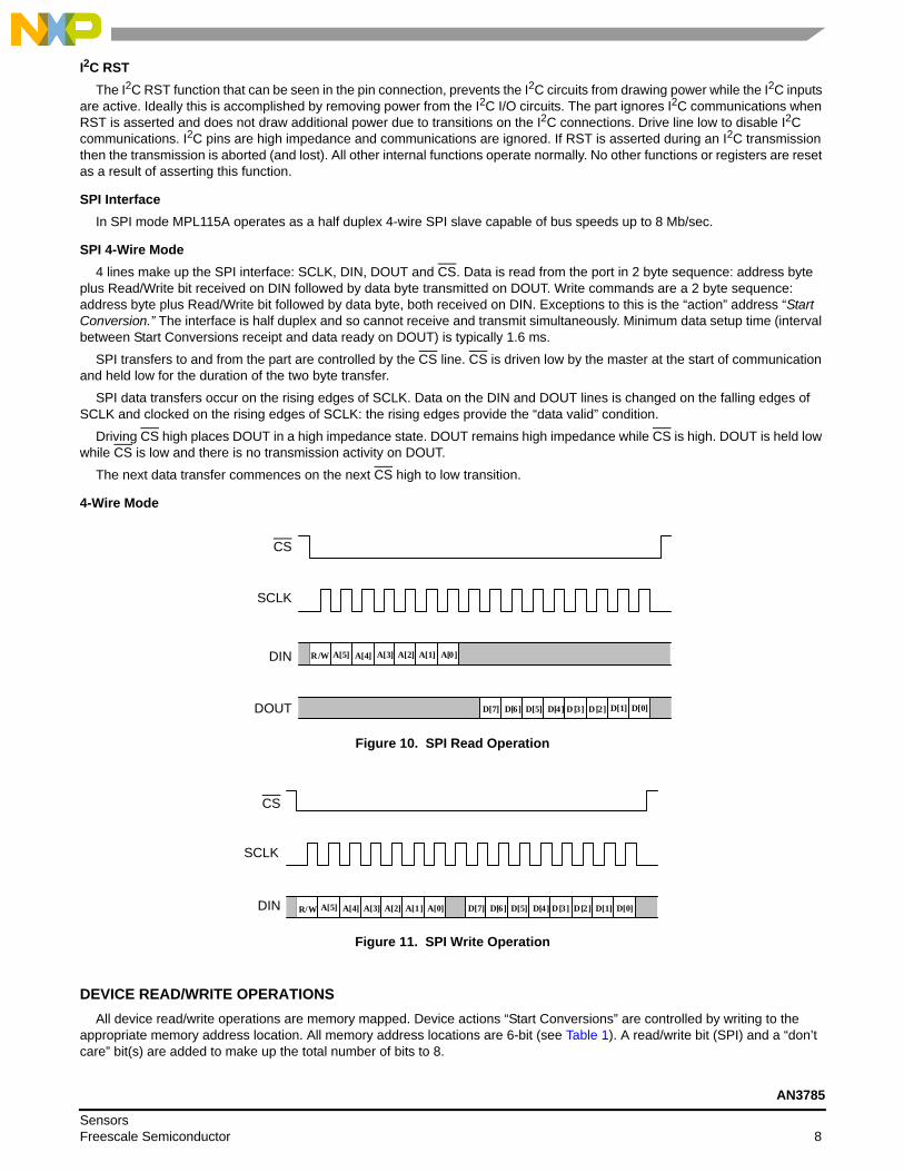
SPI Interface
In SPI mode MPL115A operates as a half duplex 4-wire SPI slave capable of bus speeds up to 8 Mbsec
SPI 4-Wire Mode
4 lines make up the SPI interface SCLK DIN DOUT and CS Data is read from the port in 2 byte sequence address byte plus ReadWrite bit received on DIN followed by data byte transmitted on DOUT Write commands are a 2 byte sequence address byte plus ReadWrite bit followed by data byte both received on DIN Exceptions to this is the ldquoactionrdquo address ldquoStart Conversionrdquo The interface is half duplex and so cannot receive and transmit simultaneously Minimum data setup time (interval between Start Conversions receipt and data ready on DOUT) is typically 16 ms
SPI transfers to and from the part are controlled by the CS line CS is driven low by the master at the start of communication and held low for the duration of the two byte transfer
SPI data transfers occur on the rising edges of SCLK Data on the DIN and DOUT lines is changed on the falling edges of SCLK and clocked on the rising edges of SCLK the rising edges provide the ldquodata validrdquo condition
Driving CS high places DOUT in a high impedance state DOUT remains high impedance while CS is high DOUT is held low while CS is low and there is no transmission activity on DOUT
The next data transfer commences on the next CS high to low transition
4-Wire Mode
Figure 10 SPI Read Operation
Figure 11 SPI Write Operation
DEVICE READWRITE OPERATIONS
All device readwrite operations are memory mapped Device actions ldquoStart Conversionsrdquo are controlled by writing to the appropriate memory address location All memory address locations are 6-bit (see Table 1) A readwrite bit (SPI) and a ldquodonrsquot carerdquo bit(s) are added to make up the total number of bits to 8
For I2C devices the MSB (bit 7) is ldquodonrsquot carerdquo and bits 6 to 0 are available for addressing eg bit 6 is always 0 with the remaining bits (50) making up the 6-bit address in MPL115A
For SPI devices the MSB is RW and the LSB is ldquodonrsquot carerdquo with the remaining bits (61) making up the 6-bit address The appropriate memory location is written toread from in response to the condition of the RW bit which is lsquo1rsquo for read operations and lsquo0rsquo for write operations
The basic device write commands are shown in Table 1 (SPI versions) and Table 2 (I2C versions) The availability of particular commands depends on the operating mode of the device There are three basic operating modes Test Debug and User (normal)
Table 2 I2C Write Commands description
Table 3 I2C Read Command Description
Table 4 SPI Write Commands
Table 1 I2C Write Commands
Command Binary HEX(1)
1 The command byte needs to be paired with a 0x00 as part of the SPI exchange to complete the passing of Start Conversions
Command
Devices Address + Write bit 11000000 0xC0 Devices Address + Write bit
Start Conversions X0010010 0x12 Start Conversions
Command Action Taken
Start Conversions
Wake main circuits Start clock Allow supply stabilization time Select pressure sensor input Apply positive sensor excitation and perform A to D conversion Select temperature input Perform A to D conversion Load the Pressure and Temperature registers with the result Shut down main circuits and clock This action takes a typical time of 16ms to complete and have data available in the Pressure and Temperature registers
Command Binary HEX(1)
1 The command byte needs to be paired with a 0x00 as part of the SPI exchange to complete the passing of Start Conversions
Device Address + Read bit 11000001 0xC1
Read Pressure MSB X0000000 0x00
Read Pressure LSB X0000001 0x01
Read Temperature MSB X0000010 0x02
Read Temperature LSB X0000011 0x03
Read Coefficient data byte 1 X0000100 0x04
X = donrsquot care
Command Binary HEX(1)
1 The command byte needs to be paired with a 0x00 as part of the SPI exchange to complete the passing of Start Conversions
Start Conversions 0010010X 0x24
X = donrsquot care
AN3785
SensorsFreescale Semiconductor 9
Table 6 Example SPI Read Commands
DEVICE MEMORY MAP
21 Pressure Temperature and Coefficient Bit-Width SpecificationsThe table below specifies the initial coefficient bit-width specifications for the compensation algorithm and the specifications for Pressure and Temperature ADC values
Table 5 SPI Write Command Description
Command Action Taken
Start Conversions
Wake main circuits Start clock Allow supply stabilization time Select pressure sensor input Apply positive sensor excitation and perform A to D conversion Select temperature input Perform A to D conversion Load the Pressure and Temperature registers with the result Shut down main circuits and clock This action takes a typical time of 16ms to complete and have data available in the Pressure and Temperature registers
Command Binary HEX(1)
1 The command byte needs to be paired with a 0x00 as part of the SPI exchange to complete the passing of stated command
Read Pressure MSB 1000000X 0x80
Read Pressure LSB 1000001X 0x82
Read Temperature MSB 1000010X 0x84
Read Temperature LSB 1000011X 0x86
Read Coefficient data byte 1 1000100X 0x88
X = donrsquot care
Table 1 Device Memory Map
Address Name Description Size (bits)
0x00 Padc_MSB 10-bit Pressure output value MSB 8
0x01 Padc_LSB 10-bit Pressure output value LSB 2
0x02 Tadc_MSB 10-bit Temperature output value MSB 8
0x03 Tadc_LSB 10-bit Temperature output value LSB 2
0x04 a0MSB a0 coefficient MSB 8
0x05 a0LSB a0 coefficient LSB 8
0x06 b1MSB b1 coefficient MSB 8
0x07 b1LSB b1 coefficient LSB 8
0x08 b2MSB b2 coefficient MSB 8
0x09 b2LSB b2 coefficient LSB 8
0x0A c12MSB c12 coefficient MSB 8
0x0B c12LSB c12 coefficient LSB 8
0x0C Reserved mdash mdash
0x0D Reserved mdash mdash
0x0E Reserved mdash mdash
0x0F Reserved mdash mdash
0x10 Reserved mdash mdash
0x11 Reserved mdash mdash
0x12 CONVERT Start both Pressure and Temperature Conversion mdash
These registers are set to 0x00 These are reserved and were previously utilized as Coefficient values now set to a value to 0x00 for simplifying compensation
AN3785
SensorsFreescale Semiconductor 10
Pressure Temperature and Compensation Coefficient Specifications
a0 b1 b2 c12 Padc Tadc
Total Bits 16 16 16 14 10 10
Sign Bits 1 1 1 1 0 0
Integer Bits 12 2 1 0 10 10
Fractional Bits 3 13 14 13 0 0
dec pt zero pad 0 0 0 9 0 0
AN3785
SensorsFreescale Semiconductor 11
Example Binary Format Definitions
a0 Signed Integer Bits = 12 Fractional Bits = 3 Coeff a0 = S I11 I10 I9 I8 I7 I6 I5 I4 I3 I2 I1 I0 F2 F1 F0
b1 Signed Integer Bits = 2 Fractional Bits = 7 Coeff b1 = S I1 I0 F12 F10 F9 F8 F7 F6 F5 F4 F3 F2 F1 F0
b2 Signed Integer Bits = 1 Fractional Bits = 14 Coeff b2 = S I0 F13 F12 F10 F9 F8 F7 F6 F5 F4 F3 F2 F1 F0
c12 Signed Integer Bits = 0 Fractional Bits = 13 dec pt zero pad = 9 Coeff c12 = S 0 000 000 000 F12 F10 F9 F8 F7 F6 F5 F4 F3 F2 F1 F0
NOTE Negative coefficients are coded in 2rsquos complement notation
22 CompensationThe 10-bit compensated pressure output Pcomp is calculated as follows
Eqn 1
Where
Padc is the 10-bit pressure ADC output of the MPL115A
Tadc is the 10-bit temperature ADC output of the MPL115A
a0 is the pressure offset coefficient
b1 is the pressure sensitivity coefficient
b2 is the 1st order temperature offset coefficient (TCO)
c12 is the coefficient for temperature sensitivity coefficient (TCS)
Pcomp will produce a value of 0 with an input pressure of 50 kPa and will produce a full-scale value of 1023 with an input pressure of 115 kPa
Eqn 2
23 Evaluation Sequence Arithmetic CircuitsThe following is an example of the calculation for Pcomp the compensated pressure output Input values are in bold
c12x2 = c12 Tadc
a1 = b1 + c12x2
a1x1 = a1 Padc
y1 = a0 + a1x1
a2x2 = b2 Tadc
Pcomp = y1 + a2x2
This can be calculated as a succession of Multiply Accumulates (MACs) operations of the form y = a + b x
Pcomp a0 b1 c12 Tadc+ Padc b2 Tadc++=
Pressure (kPa) P= comp115 50ndash
1023---------------------- 50+
a
b
x
y+
X
AN3785
SensorsFreescale Semiconductor 12
The polynomial can be evaluated (Equation 1) as a sequence of 3 MACs
I2C COMMUNICATION AND EXAMPLE
The actions taken by the part in response to each command are as follows
X = donrsquot care
These are MPL115A2 I2C commands to read coefficients execute Pressure and Temperature conversions and to read Pressure and Temperature data The sequence of the commands for the interaction is given as an example to operate the MPL115A2
Utilizing this gathered data an example of the calculating the Compensated Pressure reading is given in floating point notation
I2C Commands (simplified for communication)
Device Address + write bit ldquoTo Writerdquo = 0xC0
Device Address + read bit ldquoTo Readrdquo = 0xC1
Command to Write ldquoConvert Pressure and Temperaturerdquo = 0x12
Command to Read ldquoPressure ADC High byterdquo = 0x00
Table 2 I2C Write Command Description
Command Action Taken
Start ConversionsWake main circuits Start clock Allow supply stabilization time Select pressure sensor input Apply positive sensor excitation and perform A to D conversion Select temperature input Perform A to D conversion Load the Pressure and Temperature registers with the result Shut down main circuits and clock
Table 3 I2C Read Command Description
Command Binary HEX(1)
Device Address + Read bit 1100 0001 0xC1
Read Pressure MSB X000 0000 0x00
Read Pressure LSB X000 0001 0x01
Read Temperature MSB X000 0010 0x02
Read Temperature LSB X000 0011 0x03
Read Coefficient data byte 1 X000 0100 0x04
Pcomp a0 b1 c12 Tadc+ Padc b2 Tadc++=
b1
c12
Tadc
a0
b2
Tadc
Padc
a1
y1
y PComp
AN3785
SensorsFreescale Semiconductor 13
Command to Read ldquoPressure ADC Low byterdquo = 0x01
Command to Read ldquoTemperature ADC High byterdquo = 0x02
Command to Read ldquoTemperature ADC Low byterdquo = 0x03
Command to Read ldquoCoefficient data byte 1 High byterdquo = 0x04
25 SPI Device ReadWrite OperationsAll device readwrite operations are memory mapped Device actions eg ldquoStart Pressure Conversionrdquo are controlled by writing to the appropriate memory address location All memory address locations are 6-bit (see Table 1)
The 8-bit command word comprises
bull the most significant bit which is the ReadWrite identifier which is 1 for read operations and 0 for writesbull the 6-bit address (from Table 1)bull the least significant bit which is not used and is dont care (X)
The device write commands are shown in Table 1
The actions taken by the part in response to each command are as follows
Table 4 SPI Write Command
Command Binary HEX(1)
1 The command byte needs to be paired with a 0x00 as part of the SPI exchange to complete the passing of Start Conversions
Start Conversions 0010010X 0x24
X = donrsquot care
Table 5 SPI Write Command Description
Command Action Taken
Start Conversions
Wake main circuits Start clock Allow supply stabilization time Select pressure sensor input Apply positive sensor excitation and perform A to D conversion Select temperature input Perform A to D conversion Load the Pressure and Temperature registers with the result Shut down main circuits and clock
AN3785
SensorsFreescale Semiconductor 16
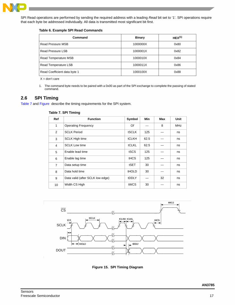
SPI Read operations are performed by sending the required address with a leading Read bit set to lsquo1rsquo SPI operations require that each byte be addressed individually All data is transmitted most significant bit first
26 SPI TimingTable 7 and Figure describe the timing requirements for the SPI system
Figure 15 SPI Timing Diagram
Table 6 Example SPI Read Commands
Command Binary HEX(1)
1 The command byte needs to be paired with a 0x00 as part of the SPI exchange to complete the passing of stated command
27 Example of SPI Reading of CoefficientsThese are MPL115A2 SPI commands to read coefficients execute Pressure and Temperature conversions and to read Pressure and Temperature data The sequence of the commands for the interaction is given as an example to operate the MPL115A2 Utilizing this gathered data an example of the calculating the Compensated Pressure reading is given in floating point notation
SPI Commands (simplified for communication)
Command to Write ldquoConvert Pressure and Temperaturerdquo = 0x24
Command to Read ldquoPressure ADC High byterdquo = 0x80
Command to Read ldquoPressure ADC Low byterdquo = 0x82
Command to Read ldquoTemperature ADC High byterdquo = 0x84
Command to Read ldquoTemperature ADC High byterdquo = 0x86
Command to Read ldquoCoefficient data byte 1 High byterdquo = 0x88
Freescale and the Freescale logo are trademarks of Freescale Semiconductor Inc
Reg US Pat amp Tm Off Xtrinsic is a trademark of Freescale Semiconductor Inc
All other product or service names are the property of their respective owners
copy 62112 Freescale Semiconductor Inc All rights reserved
AN3785Rev 6062012
RoHS-compliant andor Pb-free versions of Freescale products have the functionality and electrical characteristics of their non-RoHS-compliant andor non-Pb-free counterparts For further information see httpwwwfreescalecom or contact your Freescale sales representative
For information on Freescalersquos Environmental Products program go to httpwwwfreescalecomepp
Introduction
Product features
1 Mechanical and Electrical Specifications
11 Maximum Ratings
12 Operating Characteristics
13 Pin Connections SPI
14 Pin Connections I2C
2 Overview of FunctionsOperation
Initial Power-up
Reading Coefficient Data
Data Conversion
Compensated Pressure Reading
I2C Communication
Write Mode
Conversion Time
Read Mode
ImiddotC Read Pressure Sequence
ImiddotC Read Coefficients Sequence
I2C RST
SPI Interface
SPI 4-Wire Mode
4-Wire Mode
Device ReadWrite Operations
Device Memory Map
21 Pressure Temperature and Coefficient Bit-Width Specifications
22 Compensation
23 Evaluation Sequence Arithmetic Circuits
I2C Communication and Example
I2C Commands (simplified for communication)
Read Coefficients
24 Example of Pressure Compensated Calculation in Floating-point Notation
Pressure Compensation
Using the evaluation sequence shown in Section 33
25 SPI Device ReadWrite Operations
26 SPI Timing
27 Example of SPI Reading of Coefficients
SPI Commands (simplified for communication)
28 Example of Pressure Compensated Calculation in Floating-point Notation
The MPL115A is an absolute pressure sensor with digital output for low cost applications A miniature 5 x 3 x 12 mm LGA package ideally suits it for portable electronics and space constrained applications Low current consumptions of 5 A during Active mode and 1 A during Shutdown (Sleep) mode target battery and other low-power applications A wide operating temperature range from -40degC to +105degC fits demanding environmental requirements
MPL115A employs a MEMS pressure sensor with a conditioning IC to provide accurate pressure measurement from 50 to 115 kPa An integrated ADC provides digitized temperature and pressure sensor outputs via an I2C or SPI port Calibration Data is stored in internal ROM Utilizing raw sensor output the host microcontroller executes a compensation algorithm to render Compensated Absolute Pressure with 1 kPa accuracy
The MPL115A pressure sensorrsquos small form factor low power capability precision and digital output optimize it for barometric measurement applications
VDD
VDD1VDD1
1
AB
SW1
AB
SW1
3 2 1
C3
01UF
C3
01UF
GND1GND1
1
C1
10UF
C1
10UF
U1
MPL115A1
U1
MPL115A1
GND
3
DOUT 6DIN7
VDD
1
CS 5SCLK 8CAP2SHDN4
J4J4
1234
C2
10UF
C2
10UF
SHDN
VDD
VDDVDD
C3
01UF
C3
01UF
R1470KR1470K
AB
SW1
AB
SW1
3 2 1
U1
MPL115A2
U1
MPL115A2
GND
3
DOUT 67
VDD
1
SCL 8CAP2
VDD1VDD1
1
J1
HDR_1X2
J1
HDR_1X2
12
C1
10UF
C1
10UF
R3470KR3470K
GND1GND1
1
R2470KR2470K
C2
10UF
C2
10UF
4SHDN RST
5
SDA
AN3785
SensorsFreescale Semiconductor 2
1 Mechanical and Electrical Specifications
11 Maximum RatingsVoltage (with respect to GND unless otherwise noted)
VDD -03 V to +55 V
SHDN SCLK CS DIN DOUT -03 V to VDD+03 V
Operating Temperature Range -40degC to +105degC
Storage Temperature Range-40degC to +125degC
Overpressure 1000 kPa
12 Operating CharacteristicsVDD = 2375 V to 55 V TA = -40degC to +105degC unless otherwise noted Typical values are at VDD = 33 V TA = +25degC
Ref Parameters Symbol Conditions Min Typ Max Units
1 Operating Supply Voltage VDD 2375 33 55 V
2 Supply Current IDD Shutdown (SHDN = GND) mdash mdash 1 A
Standby mdash 35 10 A
Average ndash at one measurement per second mdash 5 6 A
Pressure Sensor
3 Range 50 mdash 115 kPa
4 Resolution mdash 015 mdash kPa
5 Accuracy -20ordmC to 85ordmC mdash mdash plusmn1 kPa
6 Power Supply Rejection Typical operating circuit at DC 01 mdash kPaV
100 mV p-p 217 Hz square wave plus 100 mV pseudo random noise with 10 MHz bandwidth
01 mdash kPa
7 Conversion Time(Start Pressure and Temperature Conversion)
tc Time between start convert command and data available in the Pressure and Temperature registers
mdash 16 3 ms
8 Wakeup Time tw Time between leaving Shutdown mode (SHDN goes high) and communicating with the device to issue a command or read data
mdash 3 5 ms
I2C IO Stages SCL SDA
9 SCL Clock Frequency fSCL mdash mdash 400 kHz
10 Low Level Input Voltage VIL mdash mdash 03VDD V
11 High Level Input Voltage VIH 07VDD mdash mdash V
I2C Outputs SDA
12 Data Setup Time tSU Setup time from command receipt to ready to transmit
0 mdash 04 s
I2C Addressing
MPL115A2 uses 7-bit addressing does not acknowledge the general call address 0000000 Slave address has been set to 0x60 or 1100000
AN3785
SensorsFreescale Semiconductor 3
13 Pin Connections SPITop View
Figure 3 Pin Connections SPI
14 Pin Connections I2CTop View
Figure 4 Pin Connections I2C
1
DOUT
DIN
VDD
CAP
SHDN
GND
CS
SCLK
2
3
4
8
7
6
5
1
NC
SDA
VDD
CAP
SHDN
GND
RST
SCL
2
3
4
8
7
6
5
AN3785
SensorsFreescale Semiconductor 4
2 Overview of FunctionsOperation
Figure 5 Sequence Flow Chart
The MPL115A interfaces to a host (or system) microcontroller in the userrsquos application All communications are via SPI or I2C A typical usage sequence is as follows
Initial Power-up
All circuit elements are active SPI or I2C port pins are high impedance and associated registers are cleared The device then enters standby mode
Reading Coefficient Data
The user then typically accesses the part and reads the coefficient data The main circuits within the slave device are disabled during read activity The coefficients are usually stored in the host microcontoller local memory but can be re-read at any time
It is suggested to read the coefficients once and store the values in the host microcontroller for speed It is not necessary to read this multiple times because the coefficients within a device are constant and do not change However note that the coefficients will be different from device to device and cannot be used for another part
Data Conversion
This is the first step that is performed each time a new pressure reading is required which is initiated by the host sending the CONVERT command The main system circuits are activated (wake) in response to the command and after the conversion completes the result is placed into the Pressure and Temperature ADC output registers
The conversion completes within the maximum conversion time tc of 16ms typical or 3ms max The device then enters standby mode
Compensated Pressure Reading
After the conversion has been given sufficient time to complete the host microcontroller reads the result from the ADC output registers and calculates the Compensated Pressure a barometricatmospheric pressure value which is compensated for changes in temperature and pressure sensor linearity This is done using the coefficient data from the MPL115A and the raw sampled pressure and temperature ADC output values in a compensation equation (detailed later) Note that this is an absolute pressure measurement with a vacuum as a reference
From this step the host controller may either wait and then return to the Data Conversion step to obtain the next pressure reading or it may go to the Shutdown step with the full supply voltage range
Reading coefficient data
Data conversion
Initial powerup
Compensated pressure reading
Shutdown
AN3785
SensorsFreescale Semiconductor 5
I2C Communication
The I2C protocol is explained below along with how to implement this pressure sensor For additional information on I2C please see AN4481 Sensors I2C Setup and FAQ I2C is compliant to the Philips I2C Bus specification version 21
The MPL115A2 uses a 7 bit device address such that in an 8 bit representation the device address is followed by a least significant bit that toggles a I2C readwrite value This leads to a I2C MPL115A2 address of 0xC0 for a write command and 0xC1 for a read command
Figure 6 MPL115A2 Commands
Write Mode
I2C writes to the device are conducted using normal I2C protocol An I2C start condition is followed by the 7-bit slave address and Write bit (0) The slave acknowledges the write request and latches the following data byte from the master Further bytes are ignored when in normal (user) mode A stop or repeat start condition must be sent by the master to complete the sequence User mode write commands include CONVERT to Start Pressure and Temperature conversion These commands are shown in Table 2 An example of the user mode I2C write sequence is shown in Figure
Figure 7 Isup2C Write Sequence ndash User Mode
Conversion Time
Note that when sending a write command to Start Conversion there is a conversion time of 16ms typical for the part to internally sample and output results After this conversion time the data will be ready to be read Before entering a repeated start or new start ensure this delay is inserted before reading new data
Read Mode
I2C reads from the device are conducted using normal I2C protocol
To read from the device the master must first send a data address or command that points to the required data To do this the master sends the 7-bit slave address + Write bit followed by data address byte Transmission is initiated by an I2C start condition and ended by either a Repeated Start or a Stop condition The master then resends the 7-bit slave address this time with a Read bit either directly following the Repeated Start condition or if the previous transmission ended with a Stop condition preceded by an I2C start condition
The slave acknowledges each byte received and proceeds to send the requested data following receipt of the second slave address The slave continues to send data incrementing the address pointer at the end of each byte The master acknowledges receipt of each byte sent by the slave and asserts a Stop (or Repeated Start) condition at the conclusion of the transmission
Examples of I2C reads for pressure data (2 bytes) and coefficient data (up to 12 bytes) are shown in Figure 7 and Figure 9
10-bit pressure and temperature data is transmitted MSB first with trailing zeros This allows the user to read only the first byte in systems that do not require the full resolution of the part and may only have limited processing capability The device continues to send data until either the transmission is complete or the master either issues a stop condition or fails to assert an acknowledge bit ie the slave treats a ldquoNakrdquo (not acknowledge) as a stop bit The master thus controls the amount of data it receives and discards any data that is not needed
MPL115A2 Commands Address
Write Command 0xC0
Read Command 0xC1
7 bit slave address plus WRITE bit
8 bit command Stop bit (or repeated start)
S D D D D D D D W Ack 0 X X X X X X X Ack P
Start Acknowledge End of Transmission
AN3785
SensorsFreescale Semiconductor 6
Isup2C Read Pressure Sequence
Figure 8 Isup2C Read Pressure Sequence
Isup2C Read Coefficients Sequence
Figure 9 Isup2C Read Coefficients Sequence
7 bit slave address plus WRITE bit
ldquoRead Pressure MSBrdquo command
7 bit slave address plus READ bit
S D D D D D D D W Ack 0 X X X X X X X Ack D D D D D D D R Ack
Start Acknowledge
10 bit pressure data with trailing zeros Stop bit
P P P P P P P P Ack P P 0 0 0 0 0 0 Nak(1)
1 The standard termination sequence is ldquoNakrdquo followed by the stop condition An ldquoAckrdquo followed by the stop condition may also be used
P
Signifies End of Transmission Slave stops sending data immediately
7 bit slave address plus WRITE bit
ldquoRead Coefficient 1rdquo command
7 bit slave address plus READ bit
S D D D D D D D W Ack X 0 0 0 0 1 0 0 Ack Sr D D D D D D R Ack
Start AcknowledgeRepeated
Start
Coefficient data first byte
Coefficient data second byte
Coefficient data third byte
Coefficient data final byte
A A A A A A A A Ack B B B B B B B B Ack C C C C C C C C Ack Ack Z Z Z Z Z Z Z Z Nak(1)
1 The standard termination sequence is ldquoNakrdquo followed by the stop condition An ldquoAckrdquo followed by the stop condition may also be used
P Ack(2)
2 Stop bit signifies end of transmission Slave stops sending data immediately
AN3785
SensorsFreescale Semiconductor 7
I2C RST
The I2C RST function that can be seen in the pin connection prevents the I2C circuits from drawing power while the I2C inputs are active Ideally this is accomplished by removing power from the I2C IO circuits The part ignores I2C communications when RST is asserted and does not draw additional power due to transitions on the I2C connections Drive line low to disable I2C communications I2C pins are high impedance and communications are ignored If RST is asserted during an I2C transmission then the transmission is aborted (and lost) All other internal functions operate normally No other functions or registers are reset as a result of asserting this function
SPI Interface
In SPI mode MPL115A operates as a half duplex 4-wire SPI slave capable of bus speeds up to 8 Mbsec
SPI 4-Wire Mode
4 lines make up the SPI interface SCLK DIN DOUT and CS Data is read from the port in 2 byte sequence address byte plus ReadWrite bit received on DIN followed by data byte transmitted on DOUT Write commands are a 2 byte sequence address byte plus ReadWrite bit followed by data byte both received on DIN Exceptions to this is the ldquoactionrdquo address ldquoStart Conversionrdquo The interface is half duplex and so cannot receive and transmit simultaneously Minimum data setup time (interval between Start Conversions receipt and data ready on DOUT) is typically 16 ms
SPI transfers to and from the part are controlled by the CS line CS is driven low by the master at the start of communication and held low for the duration of the two byte transfer
SPI data transfers occur on the rising edges of SCLK Data on the DIN and DOUT lines is changed on the falling edges of SCLK and clocked on the rising edges of SCLK the rising edges provide the ldquodata validrdquo condition
Driving CS high places DOUT in a high impedance state DOUT remains high impedance while CS is high DOUT is held low while CS is low and there is no transmission activity on DOUT
The next data transfer commences on the next CS high to low transition
4-Wire Mode
Figure 10 SPI Read Operation
Figure 11 SPI Write Operation
DEVICE READWRITE OPERATIONS
All device readwrite operations are memory mapped Device actions ldquoStart Conversionsrdquo are controlled by writing to the appropriate memory address location All memory address locations are 6-bit (see Table 1) A readwrite bit (SPI) and a ldquodonrsquot carerdquo bit(s) are added to make up the total number of bits to 8
For I2C devices the MSB (bit 7) is ldquodonrsquot carerdquo and bits 6 to 0 are available for addressing eg bit 6 is always 0 with the remaining bits (50) making up the 6-bit address in MPL115A
For SPI devices the MSB is RW and the LSB is ldquodonrsquot carerdquo with the remaining bits (61) making up the 6-bit address The appropriate memory location is written toread from in response to the condition of the RW bit which is lsquo1rsquo for read operations and lsquo0rsquo for write operations
The basic device write commands are shown in Table 1 (SPI versions) and Table 2 (I2C versions) The availability of particular commands depends on the operating mode of the device There are three basic operating modes Test Debug and User (normal)
Table 2 I2C Write Commands description
Table 3 I2C Read Command Description
Table 4 SPI Write Commands
Table 1 I2C Write Commands
Command Binary HEX(1)
1 The command byte needs to be paired with a 0x00 as part of the SPI exchange to complete the passing of Start Conversions
Command
Devices Address + Write bit 11000000 0xC0 Devices Address + Write bit
Start Conversions X0010010 0x12 Start Conversions
Command Action Taken
Start Conversions
Wake main circuits Start clock Allow supply stabilization time Select pressure sensor input Apply positive sensor excitation and perform A to D conversion Select temperature input Perform A to D conversion Load the Pressure and Temperature registers with the result Shut down main circuits and clock This action takes a typical time of 16ms to complete and have data available in the Pressure and Temperature registers
Command Binary HEX(1)
1 The command byte needs to be paired with a 0x00 as part of the SPI exchange to complete the passing of Start Conversions
Device Address + Read bit 11000001 0xC1
Read Pressure MSB X0000000 0x00
Read Pressure LSB X0000001 0x01
Read Temperature MSB X0000010 0x02
Read Temperature LSB X0000011 0x03
Read Coefficient data byte 1 X0000100 0x04
X = donrsquot care
Command Binary HEX(1)
1 The command byte needs to be paired with a 0x00 as part of the SPI exchange to complete the passing of Start Conversions
Start Conversions 0010010X 0x24
X = donrsquot care
AN3785
SensorsFreescale Semiconductor 9
Table 6 Example SPI Read Commands
DEVICE MEMORY MAP
21 Pressure Temperature and Coefficient Bit-Width SpecificationsThe table below specifies the initial coefficient bit-width specifications for the compensation algorithm and the specifications for Pressure and Temperature ADC values
Table 5 SPI Write Command Description
Command Action Taken
Start Conversions
Wake main circuits Start clock Allow supply stabilization time Select pressure sensor input Apply positive sensor excitation and perform A to D conversion Select temperature input Perform A to D conversion Load the Pressure and Temperature registers with the result Shut down main circuits and clock This action takes a typical time of 16ms to complete and have data available in the Pressure and Temperature registers
Command Binary HEX(1)
1 The command byte needs to be paired with a 0x00 as part of the SPI exchange to complete the passing of stated command
Read Pressure MSB 1000000X 0x80
Read Pressure LSB 1000001X 0x82
Read Temperature MSB 1000010X 0x84
Read Temperature LSB 1000011X 0x86
Read Coefficient data byte 1 1000100X 0x88
X = donrsquot care
Table 1 Device Memory Map
Address Name Description Size (bits)
0x00 Padc_MSB 10-bit Pressure output value MSB 8
0x01 Padc_LSB 10-bit Pressure output value LSB 2
0x02 Tadc_MSB 10-bit Temperature output value MSB 8
0x03 Tadc_LSB 10-bit Temperature output value LSB 2
0x04 a0MSB a0 coefficient MSB 8
0x05 a0LSB a0 coefficient LSB 8
0x06 b1MSB b1 coefficient MSB 8
0x07 b1LSB b1 coefficient LSB 8
0x08 b2MSB b2 coefficient MSB 8
0x09 b2LSB b2 coefficient LSB 8
0x0A c12MSB c12 coefficient MSB 8
0x0B c12LSB c12 coefficient LSB 8
0x0C Reserved mdash mdash
0x0D Reserved mdash mdash
0x0E Reserved mdash mdash
0x0F Reserved mdash mdash
0x10 Reserved mdash mdash
0x11 Reserved mdash mdash
0x12 CONVERT Start both Pressure and Temperature Conversion mdash
These registers are set to 0x00 These are reserved and were previously utilized as Coefficient values now set to a value to 0x00 for simplifying compensation
AN3785
SensorsFreescale Semiconductor 10
Pressure Temperature and Compensation Coefficient Specifications
a0 b1 b2 c12 Padc Tadc
Total Bits 16 16 16 14 10 10
Sign Bits 1 1 1 1 0 0
Integer Bits 12 2 1 0 10 10
Fractional Bits 3 13 14 13 0 0
dec pt zero pad 0 0 0 9 0 0
AN3785
SensorsFreescale Semiconductor 11
Example Binary Format Definitions
a0 Signed Integer Bits = 12 Fractional Bits = 3 Coeff a0 = S I11 I10 I9 I8 I7 I6 I5 I4 I3 I2 I1 I0 F2 F1 F0
b1 Signed Integer Bits = 2 Fractional Bits = 7 Coeff b1 = S I1 I0 F12 F10 F9 F8 F7 F6 F5 F4 F3 F2 F1 F0
b2 Signed Integer Bits = 1 Fractional Bits = 14 Coeff b2 = S I0 F13 F12 F10 F9 F8 F7 F6 F5 F4 F3 F2 F1 F0
c12 Signed Integer Bits = 0 Fractional Bits = 13 dec pt zero pad = 9 Coeff c12 = S 0 000 000 000 F12 F10 F9 F8 F7 F6 F5 F4 F3 F2 F1 F0
NOTE Negative coefficients are coded in 2rsquos complement notation
22 CompensationThe 10-bit compensated pressure output Pcomp is calculated as follows
Eqn 1
Where
Padc is the 10-bit pressure ADC output of the MPL115A
Tadc is the 10-bit temperature ADC output of the MPL115A
a0 is the pressure offset coefficient
b1 is the pressure sensitivity coefficient
b2 is the 1st order temperature offset coefficient (TCO)
c12 is the coefficient for temperature sensitivity coefficient (TCS)
Pcomp will produce a value of 0 with an input pressure of 50 kPa and will produce a full-scale value of 1023 with an input pressure of 115 kPa
Eqn 2
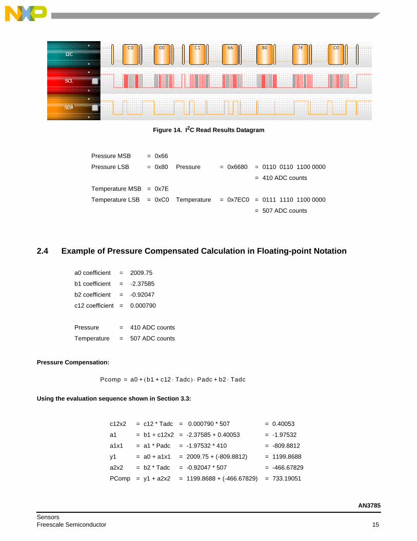
23 Evaluation Sequence Arithmetic CircuitsThe following is an example of the calculation for Pcomp the compensated pressure output Input values are in bold
c12x2 = c12 Tadc
a1 = b1 + c12x2
a1x1 = a1 Padc
y1 = a0 + a1x1
a2x2 = b2 Tadc
Pcomp = y1 + a2x2
This can be calculated as a succession of Multiply Accumulates (MACs) operations of the form y = a + b x
Pcomp a0 b1 c12 Tadc+ Padc b2 Tadc++=
Pressure (kPa) P= comp115 50ndash
1023---------------------- 50+
a
b
x
y+
X
AN3785
SensorsFreescale Semiconductor 12
The polynomial can be evaluated (Equation 1) as a sequence of 3 MACs
I2C COMMUNICATION AND EXAMPLE
The actions taken by the part in response to each command are as follows
X = donrsquot care
These are MPL115A2 I2C commands to read coefficients execute Pressure and Temperature conversions and to read Pressure and Temperature data The sequence of the commands for the interaction is given as an example to operate the MPL115A2
Utilizing this gathered data an example of the calculating the Compensated Pressure reading is given in floating point notation
I2C Commands (simplified for communication)
Device Address + write bit ldquoTo Writerdquo = 0xC0
Device Address + read bit ldquoTo Readrdquo = 0xC1
Command to Write ldquoConvert Pressure and Temperaturerdquo = 0x12
Command to Read ldquoPressure ADC High byterdquo = 0x00
Table 2 I2C Write Command Description
Command Action Taken
Start ConversionsWake main circuits Start clock Allow supply stabilization time Select pressure sensor input Apply positive sensor excitation and perform A to D conversion Select temperature input Perform A to D conversion Load the Pressure and Temperature registers with the result Shut down main circuits and clock
Table 3 I2C Read Command Description
Command Binary HEX(1)
Device Address + Read bit 1100 0001 0xC1
Read Pressure MSB X000 0000 0x00
Read Pressure LSB X000 0001 0x01
Read Temperature MSB X000 0010 0x02
Read Temperature LSB X000 0011 0x03
Read Coefficient data byte 1 X000 0100 0x04
Pcomp a0 b1 c12 Tadc+ Padc b2 Tadc++=
b1
c12
Tadc
a0
b2
Tadc
Padc
a1
y1
y PComp
AN3785
SensorsFreescale Semiconductor 13
Command to Read ldquoPressure ADC Low byterdquo = 0x01
Command to Read ldquoTemperature ADC High byterdquo = 0x02
Command to Read ldquoTemperature ADC Low byterdquo = 0x03
Command to Read ldquoCoefficient data byte 1 High byterdquo = 0x04
25 SPI Device ReadWrite OperationsAll device readwrite operations are memory mapped Device actions eg ldquoStart Pressure Conversionrdquo are controlled by writing to the appropriate memory address location All memory address locations are 6-bit (see Table 1)
The 8-bit command word comprises
bull the most significant bit which is the ReadWrite identifier which is 1 for read operations and 0 for writesbull the 6-bit address (from Table 1)bull the least significant bit which is not used and is dont care (X)
The device write commands are shown in Table 1
The actions taken by the part in response to each command are as follows
Table 4 SPI Write Command
Command Binary HEX(1)
1 The command byte needs to be paired with a 0x00 as part of the SPI exchange to complete the passing of Start Conversions
Start Conversions 0010010X 0x24
X = donrsquot care
Table 5 SPI Write Command Description
Command Action Taken
Start Conversions
Wake main circuits Start clock Allow supply stabilization time Select pressure sensor input Apply positive sensor excitation and perform A to D conversion Select temperature input Perform A to D conversion Load the Pressure and Temperature registers with the result Shut down main circuits and clock
AN3785
SensorsFreescale Semiconductor 16
SPI Read operations are performed by sending the required address with a leading Read bit set to lsquo1rsquo SPI operations require that each byte be addressed individually All data is transmitted most significant bit first
26 SPI TimingTable 7 and Figure describe the timing requirements for the SPI system
Figure 15 SPI Timing Diagram
Table 6 Example SPI Read Commands
Command Binary HEX(1)
1 The command byte needs to be paired with a 0x00 as part of the SPI exchange to complete the passing of stated command
27 Example of SPI Reading of CoefficientsThese are MPL115A2 SPI commands to read coefficients execute Pressure and Temperature conversions and to read Pressure and Temperature data The sequence of the commands for the interaction is given as an example to operate the MPL115A2 Utilizing this gathered data an example of the calculating the Compensated Pressure reading is given in floating point notation
SPI Commands (simplified for communication)
Command to Write ldquoConvert Pressure and Temperaturerdquo = 0x24
Command to Read ldquoPressure ADC High byterdquo = 0x80
Command to Read ldquoPressure ADC Low byterdquo = 0x82
Command to Read ldquoTemperature ADC High byterdquo = 0x84
Command to Read ldquoTemperature ADC High byterdquo = 0x86
Command to Read ldquoCoefficient data byte 1 High byterdquo = 0x88
Freescale and the Freescale logo are trademarks of Freescale Semiconductor Inc
Reg US Pat amp Tm Off Xtrinsic is a trademark of Freescale Semiconductor Inc
All other product or service names are the property of their respective owners
copy 62112 Freescale Semiconductor Inc All rights reserved
AN3785Rev 6062012
RoHS-compliant andor Pb-free versions of Freescale products have the functionality and electrical characteristics of their non-RoHS-compliant andor non-Pb-free counterparts For further information see httpwwwfreescalecom or contact your Freescale sales representative
For information on Freescalersquos Environmental Products program go to httpwwwfreescalecomepp
Introduction
Product features
1 Mechanical and Electrical Specifications
11 Maximum Ratings
12 Operating Characteristics
13 Pin Connections SPI
14 Pin Connections I2C
2 Overview of FunctionsOperation
Initial Power-up
Reading Coefficient Data
Data Conversion
Compensated Pressure Reading
I2C Communication
Write Mode
Conversion Time
Read Mode
ImiddotC Read Pressure Sequence
ImiddotC Read Coefficients Sequence
I2C RST
SPI Interface
SPI 4-Wire Mode
4-Wire Mode
Device ReadWrite Operations
Device Memory Map
21 Pressure Temperature and Coefficient Bit-Width Specifications
22 Compensation
23 Evaluation Sequence Arithmetic Circuits
I2C Communication and Example
I2C Commands (simplified for communication)
Read Coefficients
24 Example of Pressure Compensated Calculation in Floating-point Notation
Pressure Compensation
Using the evaluation sequence shown in Section 33
25 SPI Device ReadWrite Operations
26 SPI Timing
27 Example of SPI Reading of Coefficients
SPI Commands (simplified for communication)
28 Example of Pressure Compensated Calculation in Floating-point Notation
Using the evaluation sequence shown in Section 33
Coding Section
1 Mechanical and Electrical Specifications
11 Maximum RatingsVoltage (with respect to GND unless otherwise noted)
VDD -03 V to +55 V
SHDN SCLK CS DIN DOUT -03 V to VDD+03 V
Operating Temperature Range -40degC to +105degC
Storage Temperature Range-40degC to +125degC
Overpressure 1000 kPa
12 Operating CharacteristicsVDD = 2375 V to 55 V TA = -40degC to +105degC unless otherwise noted Typical values are at VDD = 33 V TA = +25degC
Ref Parameters Symbol Conditions Min Typ Max Units
1 Operating Supply Voltage VDD 2375 33 55 V
2 Supply Current IDD Shutdown (SHDN = GND) mdash mdash 1 A
Standby mdash 35 10 A
Average ndash at one measurement per second mdash 5 6 A
Pressure Sensor
3 Range 50 mdash 115 kPa
4 Resolution mdash 015 mdash kPa
5 Accuracy -20ordmC to 85ordmC mdash mdash plusmn1 kPa
6 Power Supply Rejection Typical operating circuit at DC 01 mdash kPaV
100 mV p-p 217 Hz square wave plus 100 mV pseudo random noise with 10 MHz bandwidth
01 mdash kPa
7 Conversion Time(Start Pressure and Temperature Conversion)
tc Time between start convert command and data available in the Pressure and Temperature registers
mdash 16 3 ms
8 Wakeup Time tw Time between leaving Shutdown mode (SHDN goes high) and communicating with the device to issue a command or read data
mdash 3 5 ms
I2C IO Stages SCL SDA
9 SCL Clock Frequency fSCL mdash mdash 400 kHz
10 Low Level Input Voltage VIL mdash mdash 03VDD V
11 High Level Input Voltage VIH 07VDD mdash mdash V
I2C Outputs SDA
12 Data Setup Time tSU Setup time from command receipt to ready to transmit
0 mdash 04 s
I2C Addressing
MPL115A2 uses 7-bit addressing does not acknowledge the general call address 0000000 Slave address has been set to 0x60 or 1100000
AN3785
SensorsFreescale Semiconductor 3
13 Pin Connections SPITop View
Figure 3 Pin Connections SPI
14 Pin Connections I2CTop View
Figure 4 Pin Connections I2C
1
DOUT
DIN
VDD
CAP
SHDN
GND
CS
SCLK
2
3
4
8
7
6
5
1
NC
SDA
VDD
CAP
SHDN
GND
RST
SCL
2
3
4
8
7
6
5
AN3785
SensorsFreescale Semiconductor 4
2 Overview of FunctionsOperation
Figure 5 Sequence Flow Chart
The MPL115A interfaces to a host (or system) microcontroller in the userrsquos application All communications are via SPI or I2C A typical usage sequence is as follows
Initial Power-up
All circuit elements are active SPI or I2C port pins are high impedance and associated registers are cleared The device then enters standby mode
Reading Coefficient Data
The user then typically accesses the part and reads the coefficient data The main circuits within the slave device are disabled during read activity The coefficients are usually stored in the host microcontoller local memory but can be re-read at any time
It is suggested to read the coefficients once and store the values in the host microcontroller for speed It is not necessary to read this multiple times because the coefficients within a device are constant and do not change However note that the coefficients will be different from device to device and cannot be used for another part
Data Conversion
This is the first step that is performed each time a new pressure reading is required which is initiated by the host sending the CONVERT command The main system circuits are activated (wake) in response to the command and after the conversion completes the result is placed into the Pressure and Temperature ADC output registers
The conversion completes within the maximum conversion time tc of 16ms typical or 3ms max The device then enters standby mode
Compensated Pressure Reading
After the conversion has been given sufficient time to complete the host microcontroller reads the result from the ADC output registers and calculates the Compensated Pressure a barometricatmospheric pressure value which is compensated for changes in temperature and pressure sensor linearity This is done using the coefficient data from the MPL115A and the raw sampled pressure and temperature ADC output values in a compensation equation (detailed later) Note that this is an absolute pressure measurement with a vacuum as a reference
From this step the host controller may either wait and then return to the Data Conversion step to obtain the next pressure reading or it may go to the Shutdown step with the full supply voltage range
Reading coefficient data
Data conversion
Initial powerup
Compensated pressure reading
Shutdown
AN3785
SensorsFreescale Semiconductor 5
I2C Communication
The I2C protocol is explained below along with how to implement this pressure sensor For additional information on I2C please see AN4481 Sensors I2C Setup and FAQ I2C is compliant to the Philips I2C Bus specification version 21
The MPL115A2 uses a 7 bit device address such that in an 8 bit representation the device address is followed by a least significant bit that toggles a I2C readwrite value This leads to a I2C MPL115A2 address of 0xC0 for a write command and 0xC1 for a read command
Figure 6 MPL115A2 Commands
Write Mode
I2C writes to the device are conducted using normal I2C protocol An I2C start condition is followed by the 7-bit slave address and Write bit (0) The slave acknowledges the write request and latches the following data byte from the master Further bytes are ignored when in normal (user) mode A stop or repeat start condition must be sent by the master to complete the sequence User mode write commands include CONVERT to Start Pressure and Temperature conversion These commands are shown in Table 2 An example of the user mode I2C write sequence is shown in Figure
Figure 7 Isup2C Write Sequence ndash User Mode
Conversion Time
Note that when sending a write command to Start Conversion there is a conversion time of 16ms typical for the part to internally sample and output results After this conversion time the data will be ready to be read Before entering a repeated start or new start ensure this delay is inserted before reading new data
Read Mode
I2C reads from the device are conducted using normal I2C protocol
To read from the device the master must first send a data address or command that points to the required data To do this the master sends the 7-bit slave address + Write bit followed by data address byte Transmission is initiated by an I2C start condition and ended by either a Repeated Start or a Stop condition The master then resends the 7-bit slave address this time with a Read bit either directly following the Repeated Start condition or if the previous transmission ended with a Stop condition preceded by an I2C start condition
The slave acknowledges each byte received and proceeds to send the requested data following receipt of the second slave address The slave continues to send data incrementing the address pointer at the end of each byte The master acknowledges receipt of each byte sent by the slave and asserts a Stop (or Repeated Start) condition at the conclusion of the transmission
Examples of I2C reads for pressure data (2 bytes) and coefficient data (up to 12 bytes) are shown in Figure 7 and Figure 9
10-bit pressure and temperature data is transmitted MSB first with trailing zeros This allows the user to read only the first byte in systems that do not require the full resolution of the part and may only have limited processing capability The device continues to send data until either the transmission is complete or the master either issues a stop condition or fails to assert an acknowledge bit ie the slave treats a ldquoNakrdquo (not acknowledge) as a stop bit The master thus controls the amount of data it receives and discards any data that is not needed
MPL115A2 Commands Address
Write Command 0xC0
Read Command 0xC1
7 bit slave address plus WRITE bit
8 bit command Stop bit (or repeated start)
S D D D D D D D W Ack 0 X X X X X X X Ack P
Start Acknowledge End of Transmission
AN3785
SensorsFreescale Semiconductor 6
Isup2C Read Pressure Sequence
Figure 8 Isup2C Read Pressure Sequence
Isup2C Read Coefficients Sequence
Figure 9 Isup2C Read Coefficients Sequence
7 bit slave address plus WRITE bit
ldquoRead Pressure MSBrdquo command
7 bit slave address plus READ bit
S D D D D D D D W Ack 0 X X X X X X X Ack D D D D D D D R Ack
Start Acknowledge
10 bit pressure data with trailing zeros Stop bit
P P P P P P P P Ack P P 0 0 0 0 0 0 Nak(1)
1 The standard termination sequence is ldquoNakrdquo followed by the stop condition An ldquoAckrdquo followed by the stop condition may also be used
P
Signifies End of Transmission Slave stops sending data immediately
7 bit slave address plus WRITE bit
ldquoRead Coefficient 1rdquo command
7 bit slave address plus READ bit
S D D D D D D D W Ack X 0 0 0 0 1 0 0 Ack Sr D D D D D D R Ack
Start AcknowledgeRepeated
Start
Coefficient data first byte
Coefficient data second byte
Coefficient data third byte
Coefficient data final byte
A A A A A A A A Ack B B B B B B B B Ack C C C C C C C C Ack Ack Z Z Z Z Z Z Z Z Nak(1)
1 The standard termination sequence is ldquoNakrdquo followed by the stop condition An ldquoAckrdquo followed by the stop condition may also be used
P Ack(2)
2 Stop bit signifies end of transmission Slave stops sending data immediately
AN3785
SensorsFreescale Semiconductor 7
I2C RST
The I2C RST function that can be seen in the pin connection prevents the I2C circuits from drawing power while the I2C inputs are active Ideally this is accomplished by removing power from the I2C IO circuits The part ignores I2C communications when RST is asserted and does not draw additional power due to transitions on the I2C connections Drive line low to disable I2C communications I2C pins are high impedance and communications are ignored If RST is asserted during an I2C transmission then the transmission is aborted (and lost) All other internal functions operate normally No other functions or registers are reset as a result of asserting this function
SPI Interface
In SPI mode MPL115A operates as a half duplex 4-wire SPI slave capable of bus speeds up to 8 Mbsec
SPI 4-Wire Mode
4 lines make up the SPI interface SCLK DIN DOUT and CS Data is read from the port in 2 byte sequence address byte plus ReadWrite bit received on DIN followed by data byte transmitted on DOUT Write commands are a 2 byte sequence address byte plus ReadWrite bit followed by data byte both received on DIN Exceptions to this is the ldquoactionrdquo address ldquoStart Conversionrdquo The interface is half duplex and so cannot receive and transmit simultaneously Minimum data setup time (interval between Start Conversions receipt and data ready on DOUT) is typically 16 ms
SPI transfers to and from the part are controlled by the CS line CS is driven low by the master at the start of communication and held low for the duration of the two byte transfer
SPI data transfers occur on the rising edges of SCLK Data on the DIN and DOUT lines is changed on the falling edges of SCLK and clocked on the rising edges of SCLK the rising edges provide the ldquodata validrdquo condition
Driving CS high places DOUT in a high impedance state DOUT remains high impedance while CS is high DOUT is held low while CS is low and there is no transmission activity on DOUT
The next data transfer commences on the next CS high to low transition
4-Wire Mode
Figure 10 SPI Read Operation
Figure 11 SPI Write Operation
DEVICE READWRITE OPERATIONS
All device readwrite operations are memory mapped Device actions ldquoStart Conversionsrdquo are controlled by writing to the appropriate memory address location All memory address locations are 6-bit (see Table 1) A readwrite bit (SPI) and a ldquodonrsquot carerdquo bit(s) are added to make up the total number of bits to 8
For I2C devices the MSB (bit 7) is ldquodonrsquot carerdquo and bits 6 to 0 are available for addressing eg bit 6 is always 0 with the remaining bits (50) making up the 6-bit address in MPL115A
For SPI devices the MSB is RW and the LSB is ldquodonrsquot carerdquo with the remaining bits (61) making up the 6-bit address The appropriate memory location is written toread from in response to the condition of the RW bit which is lsquo1rsquo for read operations and lsquo0rsquo for write operations
The basic device write commands are shown in Table 1 (SPI versions) and Table 2 (I2C versions) The availability of particular commands depends on the operating mode of the device There are three basic operating modes Test Debug and User (normal)
Table 2 I2C Write Commands description
Table 3 I2C Read Command Description
Table 4 SPI Write Commands
Table 1 I2C Write Commands
Command Binary HEX(1)
1 The command byte needs to be paired with a 0x00 as part of the SPI exchange to complete the passing of Start Conversions
Command
Devices Address + Write bit 11000000 0xC0 Devices Address + Write bit
Start Conversions X0010010 0x12 Start Conversions
Command Action Taken
Start Conversions
Wake main circuits Start clock Allow supply stabilization time Select pressure sensor input Apply positive sensor excitation and perform A to D conversion Select temperature input Perform A to D conversion Load the Pressure and Temperature registers with the result Shut down main circuits and clock This action takes a typical time of 16ms to complete and have data available in the Pressure and Temperature registers
Command Binary HEX(1)
1 The command byte needs to be paired with a 0x00 as part of the SPI exchange to complete the passing of Start Conversions
Device Address + Read bit 11000001 0xC1
Read Pressure MSB X0000000 0x00
Read Pressure LSB X0000001 0x01
Read Temperature MSB X0000010 0x02
Read Temperature LSB X0000011 0x03
Read Coefficient data byte 1 X0000100 0x04
X = donrsquot care
Command Binary HEX(1)
1 The command byte needs to be paired with a 0x00 as part of the SPI exchange to complete the passing of Start Conversions
Start Conversions 0010010X 0x24
X = donrsquot care
AN3785
SensorsFreescale Semiconductor 9
Table 6 Example SPI Read Commands
DEVICE MEMORY MAP
21 Pressure Temperature and Coefficient Bit-Width SpecificationsThe table below specifies the initial coefficient bit-width specifications for the compensation algorithm and the specifications for Pressure and Temperature ADC values
Table 5 SPI Write Command Description
Command Action Taken
Start Conversions
Wake main circuits Start clock Allow supply stabilization time Select pressure sensor input Apply positive sensor excitation and perform A to D conversion Select temperature input Perform A to D conversion Load the Pressure and Temperature registers with the result Shut down main circuits and clock This action takes a typical time of 16ms to complete and have data available in the Pressure and Temperature registers
Command Binary HEX(1)
1 The command byte needs to be paired with a 0x00 as part of the SPI exchange to complete the passing of stated command
Read Pressure MSB 1000000X 0x80
Read Pressure LSB 1000001X 0x82
Read Temperature MSB 1000010X 0x84
Read Temperature LSB 1000011X 0x86
Read Coefficient data byte 1 1000100X 0x88
X = donrsquot care
Table 1 Device Memory Map
Address Name Description Size (bits)
0x00 Padc_MSB 10-bit Pressure output value MSB 8
0x01 Padc_LSB 10-bit Pressure output value LSB 2
0x02 Tadc_MSB 10-bit Temperature output value MSB 8
0x03 Tadc_LSB 10-bit Temperature output value LSB 2
0x04 a0MSB a0 coefficient MSB 8
0x05 a0LSB a0 coefficient LSB 8
0x06 b1MSB b1 coefficient MSB 8
0x07 b1LSB b1 coefficient LSB 8
0x08 b2MSB b2 coefficient MSB 8
0x09 b2LSB b2 coefficient LSB 8
0x0A c12MSB c12 coefficient MSB 8
0x0B c12LSB c12 coefficient LSB 8
0x0C Reserved mdash mdash
0x0D Reserved mdash mdash
0x0E Reserved mdash mdash
0x0F Reserved mdash mdash
0x10 Reserved mdash mdash
0x11 Reserved mdash mdash
0x12 CONVERT Start both Pressure and Temperature Conversion mdash
These registers are set to 0x00 These are reserved and were previously utilized as Coefficient values now set to a value to 0x00 for simplifying compensation
AN3785
SensorsFreescale Semiconductor 10
Pressure Temperature and Compensation Coefficient Specifications
a0 b1 b2 c12 Padc Tadc
Total Bits 16 16 16 14 10 10
Sign Bits 1 1 1 1 0 0
Integer Bits 12 2 1 0 10 10
Fractional Bits 3 13 14 13 0 0
dec pt zero pad 0 0 0 9 0 0
AN3785
SensorsFreescale Semiconductor 11
Example Binary Format Definitions
a0 Signed Integer Bits = 12 Fractional Bits = 3 Coeff a0 = S I11 I10 I9 I8 I7 I6 I5 I4 I3 I2 I1 I0 F2 F1 F0
b1 Signed Integer Bits = 2 Fractional Bits = 7 Coeff b1 = S I1 I0 F12 F10 F9 F8 F7 F6 F5 F4 F3 F2 F1 F0
b2 Signed Integer Bits = 1 Fractional Bits = 14 Coeff b2 = S I0 F13 F12 F10 F9 F8 F7 F6 F5 F4 F3 F2 F1 F0
c12 Signed Integer Bits = 0 Fractional Bits = 13 dec pt zero pad = 9 Coeff c12 = S 0 000 000 000 F12 F10 F9 F8 F7 F6 F5 F4 F3 F2 F1 F0
NOTE Negative coefficients are coded in 2rsquos complement notation
22 CompensationThe 10-bit compensated pressure output Pcomp is calculated as follows
Eqn 1
Where
Padc is the 10-bit pressure ADC output of the MPL115A
Tadc is the 10-bit temperature ADC output of the MPL115A
a0 is the pressure offset coefficient
b1 is the pressure sensitivity coefficient
b2 is the 1st order temperature offset coefficient (TCO)
c12 is the coefficient for temperature sensitivity coefficient (TCS)
Pcomp will produce a value of 0 with an input pressure of 50 kPa and will produce a full-scale value of 1023 with an input pressure of 115 kPa
Eqn 2
23 Evaluation Sequence Arithmetic CircuitsThe following is an example of the calculation for Pcomp the compensated pressure output Input values are in bold
c12x2 = c12 Tadc
a1 = b1 + c12x2
a1x1 = a1 Padc
y1 = a0 + a1x1
a2x2 = b2 Tadc
Pcomp = y1 + a2x2
This can be calculated as a succession of Multiply Accumulates (MACs) operations of the form y = a + b x
Pcomp a0 b1 c12 Tadc+ Padc b2 Tadc++=
Pressure (kPa) P= comp115 50ndash
1023---------------------- 50+
a
b
x
y+
X
AN3785
SensorsFreescale Semiconductor 12
The polynomial can be evaluated (Equation 1) as a sequence of 3 MACs
I2C COMMUNICATION AND EXAMPLE
The actions taken by the part in response to each command are as follows
X = donrsquot care
These are MPL115A2 I2C commands to read coefficients execute Pressure and Temperature conversions and to read Pressure and Temperature data The sequence of the commands for the interaction is given as an example to operate the MPL115A2
Utilizing this gathered data an example of the calculating the Compensated Pressure reading is given in floating point notation
I2C Commands (simplified for communication)
Device Address + write bit ldquoTo Writerdquo = 0xC0
Device Address + read bit ldquoTo Readrdquo = 0xC1
Command to Write ldquoConvert Pressure and Temperaturerdquo = 0x12
Command to Read ldquoPressure ADC High byterdquo = 0x00
Table 2 I2C Write Command Description
Command Action Taken
Start ConversionsWake main circuits Start clock Allow supply stabilization time Select pressure sensor input Apply positive sensor excitation and perform A to D conversion Select temperature input Perform A to D conversion Load the Pressure and Temperature registers with the result Shut down main circuits and clock
Table 3 I2C Read Command Description
Command Binary HEX(1)
Device Address + Read bit 1100 0001 0xC1
Read Pressure MSB X000 0000 0x00
Read Pressure LSB X000 0001 0x01
Read Temperature MSB X000 0010 0x02
Read Temperature LSB X000 0011 0x03
Read Coefficient data byte 1 X000 0100 0x04
Pcomp a0 b1 c12 Tadc+ Padc b2 Tadc++=
b1
c12
Tadc
a0
b2
Tadc
Padc
a1
y1
y PComp
AN3785
SensorsFreescale Semiconductor 13
Command to Read ldquoPressure ADC Low byterdquo = 0x01
Command to Read ldquoTemperature ADC High byterdquo = 0x02
Command to Read ldquoTemperature ADC Low byterdquo = 0x03
Command to Read ldquoCoefficient data byte 1 High byterdquo = 0x04
25 SPI Device ReadWrite OperationsAll device readwrite operations are memory mapped Device actions eg ldquoStart Pressure Conversionrdquo are controlled by writing to the appropriate memory address location All memory address locations are 6-bit (see Table 1)
The 8-bit command word comprises
bull the most significant bit which is the ReadWrite identifier which is 1 for read operations and 0 for writesbull the 6-bit address (from Table 1)bull the least significant bit which is not used and is dont care (X)
The device write commands are shown in Table 1
The actions taken by the part in response to each command are as follows
Table 4 SPI Write Command
Command Binary HEX(1)
1 The command byte needs to be paired with a 0x00 as part of the SPI exchange to complete the passing of Start Conversions
Start Conversions 0010010X 0x24
X = donrsquot care
Table 5 SPI Write Command Description
Command Action Taken
Start Conversions
Wake main circuits Start clock Allow supply stabilization time Select pressure sensor input Apply positive sensor excitation and perform A to D conversion Select temperature input Perform A to D conversion Load the Pressure and Temperature registers with the result Shut down main circuits and clock
AN3785
SensorsFreescale Semiconductor 16
SPI Read operations are performed by sending the required address with a leading Read bit set to lsquo1rsquo SPI operations require that each byte be addressed individually All data is transmitted most significant bit first
26 SPI TimingTable 7 and Figure describe the timing requirements for the SPI system
Figure 15 SPI Timing Diagram
Table 6 Example SPI Read Commands
Command Binary HEX(1)
1 The command byte needs to be paired with a 0x00 as part of the SPI exchange to complete the passing of stated command
27 Example of SPI Reading of CoefficientsThese are MPL115A2 SPI commands to read coefficients execute Pressure and Temperature conversions and to read Pressure and Temperature data The sequence of the commands for the interaction is given as an example to operate the MPL115A2 Utilizing this gathered data an example of the calculating the Compensated Pressure reading is given in floating point notation
SPI Commands (simplified for communication)
Command to Write ldquoConvert Pressure and Temperaturerdquo = 0x24
Command to Read ldquoPressure ADC High byterdquo = 0x80
Command to Read ldquoPressure ADC Low byterdquo = 0x82
Command to Read ldquoTemperature ADC High byterdquo = 0x84
Command to Read ldquoTemperature ADC High byterdquo = 0x86
Command to Read ldquoCoefficient data byte 1 High byterdquo = 0x88
Freescale and the Freescale logo are trademarks of Freescale Semiconductor Inc
Reg US Pat amp Tm Off Xtrinsic is a trademark of Freescale Semiconductor Inc
All other product or service names are the property of their respective owners
copy 62112 Freescale Semiconductor Inc All rights reserved
AN3785Rev 6062012
RoHS-compliant andor Pb-free versions of Freescale products have the functionality and electrical characteristics of their non-RoHS-compliant andor non-Pb-free counterparts For further information see httpwwwfreescalecom or contact your Freescale sales representative
For information on Freescalersquos Environmental Products program go to httpwwwfreescalecomepp
Introduction
Product features
1 Mechanical and Electrical Specifications
11 Maximum Ratings
12 Operating Characteristics
13 Pin Connections SPI
14 Pin Connections I2C
2 Overview of FunctionsOperation
Initial Power-up
Reading Coefficient Data
Data Conversion
Compensated Pressure Reading
I2C Communication
Write Mode
Conversion Time
Read Mode
ImiddotC Read Pressure Sequence
ImiddotC Read Coefficients Sequence
I2C RST
SPI Interface
SPI 4-Wire Mode
4-Wire Mode
Device ReadWrite Operations
Device Memory Map
21 Pressure Temperature and Coefficient Bit-Width Specifications
22 Compensation
23 Evaluation Sequence Arithmetic Circuits
I2C Communication and Example
I2C Commands (simplified for communication)
Read Coefficients
24 Example of Pressure Compensated Calculation in Floating-point Notation
Pressure Compensation
Using the evaluation sequence shown in Section 33
25 SPI Device ReadWrite Operations
26 SPI Timing
27 Example of SPI Reading of Coefficients
SPI Commands (simplified for communication)
28 Example of Pressure Compensated Calculation in Floating-point Notation
Using the evaluation sequence shown in Section 33
Coding Section
2 Overview of FunctionsOperation
Figure 5 Sequence Flow Chart
The MPL115A interfaces to a host (or system) microcontroller in the userrsquos application All communications are via SPI or I2C A typical usage sequence is as follows
Initial Power-up
All circuit elements are active SPI or I2C port pins are high impedance and associated registers are cleared The device then enters standby mode
Reading Coefficient Data
The user then typically accesses the part and reads the coefficient data The main circuits within the slave device are disabled during read activity The coefficients are usually stored in the host microcontoller local memory but can be re-read at any time
It is suggested to read the coefficients once and store the values in the host microcontroller for speed It is not necessary to read this multiple times because the coefficients within a device are constant and do not change However note that the coefficients will be different from device to device and cannot be used for another part
Data Conversion
This is the first step that is performed each time a new pressure reading is required which is initiated by the host sending the CONVERT command The main system circuits are activated (wake) in response to the command and after the conversion completes the result is placed into the Pressure and Temperature ADC output registers
The conversion completes within the maximum conversion time tc of 16ms typical or 3ms max The device then enters standby mode
Compensated Pressure Reading
After the conversion has been given sufficient time to complete the host microcontroller reads the result from the ADC output registers and calculates the Compensated Pressure a barometricatmospheric pressure value which is compensated for changes in temperature and pressure sensor linearity This is done using the coefficient data from the MPL115A and the raw sampled pressure and temperature ADC output values in a compensation equation (detailed later) Note that this is an absolute pressure measurement with a vacuum as a reference
From this step the host controller may either wait and then return to the Data Conversion step to obtain the next pressure reading or it may go to the Shutdown step with the full supply voltage range
Reading coefficient data
Data conversion
Initial powerup
Compensated pressure reading
Shutdown
AN3785
SensorsFreescale Semiconductor 5
I2C Communication
The I2C protocol is explained below along with how to implement this pressure sensor For additional information on I2C please see AN4481 Sensors I2C Setup and FAQ I2C is compliant to the Philips I2C Bus specification version 21
The MPL115A2 uses a 7 bit device address such that in an 8 bit representation the device address is followed by a least significant bit that toggles a I2C readwrite value This leads to a I2C MPL115A2 address of 0xC0 for a write command and 0xC1 for a read command
Figure 6 MPL115A2 Commands
Write Mode
I2C writes to the device are conducted using normal I2C protocol An I2C start condition is followed by the 7-bit slave address and Write bit (0) The slave acknowledges the write request and latches the following data byte from the master Further bytes are ignored when in normal (user) mode A stop or repeat start condition must be sent by the master to complete the sequence User mode write commands include CONVERT to Start Pressure and Temperature conversion These commands are shown in Table 2 An example of the user mode I2C write sequence is shown in Figure
Figure 7 Isup2C Write Sequence ndash User Mode
Conversion Time
Note that when sending a write command to Start Conversion there is a conversion time of 16ms typical for the part to internally sample and output results After this conversion time the data will be ready to be read Before entering a repeated start or new start ensure this delay is inserted before reading new data
Read Mode
I2C reads from the device are conducted using normal I2C protocol
To read from the device the master must first send a data address or command that points to the required data To do this the master sends the 7-bit slave address + Write bit followed by data address byte Transmission is initiated by an I2C start condition and ended by either a Repeated Start or a Stop condition The master then resends the 7-bit slave address this time with a Read bit either directly following the Repeated Start condition or if the previous transmission ended with a Stop condition preceded by an I2C start condition
The slave acknowledges each byte received and proceeds to send the requested data following receipt of the second slave address The slave continues to send data incrementing the address pointer at the end of each byte The master acknowledges receipt of each byte sent by the slave and asserts a Stop (or Repeated Start) condition at the conclusion of the transmission
Examples of I2C reads for pressure data (2 bytes) and coefficient data (up to 12 bytes) are shown in Figure 7 and Figure 9
10-bit pressure and temperature data is transmitted MSB first with trailing zeros This allows the user to read only the first byte in systems that do not require the full resolution of the part and may only have limited processing capability The device continues to send data until either the transmission is complete or the master either issues a stop condition or fails to assert an acknowledge bit ie the slave treats a ldquoNakrdquo (not acknowledge) as a stop bit The master thus controls the amount of data it receives and discards any data that is not needed
MPL115A2 Commands Address
Write Command 0xC0
Read Command 0xC1
7 bit slave address plus WRITE bit
8 bit command Stop bit (or repeated start)
S D D D D D D D W Ack 0 X X X X X X X Ack P
Start Acknowledge End of Transmission
AN3785
SensorsFreescale Semiconductor 6
Isup2C Read Pressure Sequence
Figure 8 Isup2C Read Pressure Sequence
Isup2C Read Coefficients Sequence
Figure 9 Isup2C Read Coefficients Sequence
7 bit slave address plus WRITE bit
ldquoRead Pressure MSBrdquo command
7 bit slave address plus READ bit
S D D D D D D D W Ack 0 X X X X X X X Ack D D D D D D D R Ack
Start Acknowledge
10 bit pressure data with trailing zeros Stop bit
P P P P P P P P Ack P P 0 0 0 0 0 0 Nak(1)
1 The standard termination sequence is ldquoNakrdquo followed by the stop condition An ldquoAckrdquo followed by the stop condition may also be used
P
Signifies End of Transmission Slave stops sending data immediately
7 bit slave address plus WRITE bit
ldquoRead Coefficient 1rdquo command
7 bit slave address plus READ bit
S D D D D D D D W Ack X 0 0 0 0 1 0 0 Ack Sr D D D D D D R Ack
Start AcknowledgeRepeated
Start
Coefficient data first byte
Coefficient data second byte
Coefficient data third byte
Coefficient data final byte
A A A A A A A A Ack B B B B B B B B Ack C C C C C C C C Ack Ack Z Z Z Z Z Z Z Z Nak(1)
1 The standard termination sequence is ldquoNakrdquo followed by the stop condition An ldquoAckrdquo followed by the stop condition may also be used
P Ack(2)
2 Stop bit signifies end of transmission Slave stops sending data immediately
AN3785
SensorsFreescale Semiconductor 7
I2C RST
The I2C RST function that can be seen in the pin connection prevents the I2C circuits from drawing power while the I2C inputs are active Ideally this is accomplished by removing power from the I2C IO circuits The part ignores I2C communications when RST is asserted and does not draw additional power due to transitions on the I2C connections Drive line low to disable I2C communications I2C pins are high impedance and communications are ignored If RST is asserted during an I2C transmission then the transmission is aborted (and lost) All other internal functions operate normally No other functions or registers are reset as a result of asserting this function
SPI Interface
In SPI mode MPL115A operates as a half duplex 4-wire SPI slave capable of bus speeds up to 8 Mbsec
SPI 4-Wire Mode
4 lines make up the SPI interface SCLK DIN DOUT and CS Data is read from the port in 2 byte sequence address byte plus ReadWrite bit received on DIN followed by data byte transmitted on DOUT Write commands are a 2 byte sequence address byte plus ReadWrite bit followed by data byte both received on DIN Exceptions to this is the ldquoactionrdquo address ldquoStart Conversionrdquo The interface is half duplex and so cannot receive and transmit simultaneously Minimum data setup time (interval between Start Conversions receipt and data ready on DOUT) is typically 16 ms
SPI transfers to and from the part are controlled by the CS line CS is driven low by the master at the start of communication and held low for the duration of the two byte transfer
SPI data transfers occur on the rising edges of SCLK Data on the DIN and DOUT lines is changed on the falling edges of SCLK and clocked on the rising edges of SCLK the rising edges provide the ldquodata validrdquo condition
Driving CS high places DOUT in a high impedance state DOUT remains high impedance while CS is high DOUT is held low while CS is low and there is no transmission activity on DOUT
The next data transfer commences on the next CS high to low transition
4-Wire Mode
Figure 10 SPI Read Operation
Figure 11 SPI Write Operation
DEVICE READWRITE OPERATIONS
All device readwrite operations are memory mapped Device actions ldquoStart Conversionsrdquo are controlled by writing to the appropriate memory address location All memory address locations are 6-bit (see Table 1) A readwrite bit (SPI) and a ldquodonrsquot carerdquo bit(s) are added to make up the total number of bits to 8
For I2C devices the MSB (bit 7) is ldquodonrsquot carerdquo and bits 6 to 0 are available for addressing eg bit 6 is always 0 with the remaining bits (50) making up the 6-bit address in MPL115A
For SPI devices the MSB is RW and the LSB is ldquodonrsquot carerdquo with the remaining bits (61) making up the 6-bit address The appropriate memory location is written toread from in response to the condition of the RW bit which is lsquo1rsquo for read operations and lsquo0rsquo for write operations
The basic device write commands are shown in Table 1 (SPI versions) and Table 2 (I2C versions) The availability of particular commands depends on the operating mode of the device There are three basic operating modes Test Debug and User (normal)
Table 2 I2C Write Commands description
Table 3 I2C Read Command Description
Table 4 SPI Write Commands
Table 1 I2C Write Commands
Command Binary HEX(1)
1 The command byte needs to be paired with a 0x00 as part of the SPI exchange to complete the passing of Start Conversions
Command
Devices Address + Write bit 11000000 0xC0 Devices Address + Write bit
Start Conversions X0010010 0x12 Start Conversions
Command Action Taken
Start Conversions
Wake main circuits Start clock Allow supply stabilization time Select pressure sensor input Apply positive sensor excitation and perform A to D conversion Select temperature input Perform A to D conversion Load the Pressure and Temperature registers with the result Shut down main circuits and clock This action takes a typical time of 16ms to complete and have data available in the Pressure and Temperature registers
Command Binary HEX(1)
1 The command byte needs to be paired with a 0x00 as part of the SPI exchange to complete the passing of Start Conversions
Device Address + Read bit 11000001 0xC1
Read Pressure MSB X0000000 0x00
Read Pressure LSB X0000001 0x01
Read Temperature MSB X0000010 0x02
Read Temperature LSB X0000011 0x03
Read Coefficient data byte 1 X0000100 0x04
X = donrsquot care
Command Binary HEX(1)
1 The command byte needs to be paired with a 0x00 as part of the SPI exchange to complete the passing of Start Conversions
Start Conversions 0010010X 0x24
X = donrsquot care
AN3785
SensorsFreescale Semiconductor 9
Table 6 Example SPI Read Commands
DEVICE MEMORY MAP
21 Pressure Temperature and Coefficient Bit-Width SpecificationsThe table below specifies the initial coefficient bit-width specifications for the compensation algorithm and the specifications for Pressure and Temperature ADC values
Table 5 SPI Write Command Description
Command Action Taken
Start Conversions
Wake main circuits Start clock Allow supply stabilization time Select pressure sensor input Apply positive sensor excitation and perform A to D conversion Select temperature input Perform A to D conversion Load the Pressure and Temperature registers with the result Shut down main circuits and clock This action takes a typical time of 16ms to complete and have data available in the Pressure and Temperature registers
Command Binary HEX(1)
1 The command byte needs to be paired with a 0x00 as part of the SPI exchange to complete the passing of stated command
Read Pressure MSB 1000000X 0x80
Read Pressure LSB 1000001X 0x82
Read Temperature MSB 1000010X 0x84
Read Temperature LSB 1000011X 0x86
Read Coefficient data byte 1 1000100X 0x88
X = donrsquot care
Table 1 Device Memory Map
Address Name Description Size (bits)
0x00 Padc_MSB 10-bit Pressure output value MSB 8
0x01 Padc_LSB 10-bit Pressure output value LSB 2
0x02 Tadc_MSB 10-bit Temperature output value MSB 8
0x03 Tadc_LSB 10-bit Temperature output value LSB 2
0x04 a0MSB a0 coefficient MSB 8
0x05 a0LSB a0 coefficient LSB 8
0x06 b1MSB b1 coefficient MSB 8
0x07 b1LSB b1 coefficient LSB 8
0x08 b2MSB b2 coefficient MSB 8
0x09 b2LSB b2 coefficient LSB 8
0x0A c12MSB c12 coefficient MSB 8
0x0B c12LSB c12 coefficient LSB 8
0x0C Reserved mdash mdash
0x0D Reserved mdash mdash
0x0E Reserved mdash mdash
0x0F Reserved mdash mdash
0x10 Reserved mdash mdash
0x11 Reserved mdash mdash
0x12 CONVERT Start both Pressure and Temperature Conversion mdash
These registers are set to 0x00 These are reserved and were previously utilized as Coefficient values now set to a value to 0x00 for simplifying compensation
AN3785
SensorsFreescale Semiconductor 10
Pressure Temperature and Compensation Coefficient Specifications
a0 b1 b2 c12 Padc Tadc
Total Bits 16 16 16 14 10 10
Sign Bits 1 1 1 1 0 0
Integer Bits 12 2 1 0 10 10
Fractional Bits 3 13 14 13 0 0
dec pt zero pad 0 0 0 9 0 0
AN3785
SensorsFreescale Semiconductor 11
Example Binary Format Definitions
a0 Signed Integer Bits = 12 Fractional Bits = 3 Coeff a0 = S I11 I10 I9 I8 I7 I6 I5 I4 I3 I2 I1 I0 F2 F1 F0
b1 Signed Integer Bits = 2 Fractional Bits = 7 Coeff b1 = S I1 I0 F12 F10 F9 F8 F7 F6 F5 F4 F3 F2 F1 F0
b2 Signed Integer Bits = 1 Fractional Bits = 14 Coeff b2 = S I0 F13 F12 F10 F9 F8 F7 F6 F5 F4 F3 F2 F1 F0
c12 Signed Integer Bits = 0 Fractional Bits = 13 dec pt zero pad = 9 Coeff c12 = S 0 000 000 000 F12 F10 F9 F8 F7 F6 F5 F4 F3 F2 F1 F0
NOTE Negative coefficients are coded in 2rsquos complement notation
22 CompensationThe 10-bit compensated pressure output Pcomp is calculated as follows
Eqn 1
Where
Padc is the 10-bit pressure ADC output of the MPL115A
Tadc is the 10-bit temperature ADC output of the MPL115A
a0 is the pressure offset coefficient
b1 is the pressure sensitivity coefficient
b2 is the 1st order temperature offset coefficient (TCO)
c12 is the coefficient for temperature sensitivity coefficient (TCS)
Pcomp will produce a value of 0 with an input pressure of 50 kPa and will produce a full-scale value of 1023 with an input pressure of 115 kPa
Eqn 2
23 Evaluation Sequence Arithmetic CircuitsThe following is an example of the calculation for Pcomp the compensated pressure output Input values are in bold
c12x2 = c12 Tadc
a1 = b1 + c12x2
a1x1 = a1 Padc
y1 = a0 + a1x1
a2x2 = b2 Tadc
Pcomp = y1 + a2x2
This can be calculated as a succession of Multiply Accumulates (MACs) operations of the form y = a + b x
Pcomp a0 b1 c12 Tadc+ Padc b2 Tadc++=
Pressure (kPa) P= comp115 50ndash
1023---------------------- 50+
a
b
x
y+
X
AN3785
SensorsFreescale Semiconductor 12
The polynomial can be evaluated (Equation 1) as a sequence of 3 MACs
I2C COMMUNICATION AND EXAMPLE
The actions taken by the part in response to each command are as follows
X = donrsquot care
These are MPL115A2 I2C commands to read coefficients execute Pressure and Temperature conversions and to read Pressure and Temperature data The sequence of the commands for the interaction is given as an example to operate the MPL115A2
Utilizing this gathered data an example of the calculating the Compensated Pressure reading is given in floating point notation
I2C Commands (simplified for communication)
Device Address + write bit ldquoTo Writerdquo = 0xC0
Device Address + read bit ldquoTo Readrdquo = 0xC1
Command to Write ldquoConvert Pressure and Temperaturerdquo = 0x12
Command to Read ldquoPressure ADC High byterdquo = 0x00
Table 2 I2C Write Command Description
Command Action Taken
Start ConversionsWake main circuits Start clock Allow supply stabilization time Select pressure sensor input Apply positive sensor excitation and perform A to D conversion Select temperature input Perform A to D conversion Load the Pressure and Temperature registers with the result Shut down main circuits and clock
Table 3 I2C Read Command Description
Command Binary HEX(1)
Device Address + Read bit 1100 0001 0xC1
Read Pressure MSB X000 0000 0x00
Read Pressure LSB X000 0001 0x01
Read Temperature MSB X000 0010 0x02
Read Temperature LSB X000 0011 0x03
Read Coefficient data byte 1 X000 0100 0x04
Pcomp a0 b1 c12 Tadc+ Padc b2 Tadc++=
b1
c12
Tadc
a0
b2
Tadc
Padc
a1
y1
y PComp
AN3785
SensorsFreescale Semiconductor 13
Command to Read ldquoPressure ADC Low byterdquo = 0x01
Command to Read ldquoTemperature ADC High byterdquo = 0x02
Command to Read ldquoTemperature ADC Low byterdquo = 0x03
Command to Read ldquoCoefficient data byte 1 High byterdquo = 0x04
25 SPI Device ReadWrite OperationsAll device readwrite operations are memory mapped Device actions eg ldquoStart Pressure Conversionrdquo are controlled by writing to the appropriate memory address location All memory address locations are 6-bit (see Table 1)
The 8-bit command word comprises
bull the most significant bit which is the ReadWrite identifier which is 1 for read operations and 0 for writesbull the 6-bit address (from Table 1)bull the least significant bit which is not used and is dont care (X)
The device write commands are shown in Table 1
The actions taken by the part in response to each command are as follows
Table 4 SPI Write Command
Command Binary HEX(1)
1 The command byte needs to be paired with a 0x00 as part of the SPI exchange to complete the passing of Start Conversions
Start Conversions 0010010X 0x24
X = donrsquot care
Table 5 SPI Write Command Description
Command Action Taken
Start Conversions
Wake main circuits Start clock Allow supply stabilization time Select pressure sensor input Apply positive sensor excitation and perform A to D conversion Select temperature input Perform A to D conversion Load the Pressure and Temperature registers with the result Shut down main circuits and clock
AN3785
SensorsFreescale Semiconductor 16
SPI Read operations are performed by sending the required address with a leading Read bit set to lsquo1rsquo SPI operations require that each byte be addressed individually All data is transmitted most significant bit first
26 SPI TimingTable 7 and Figure describe the timing requirements for the SPI system
Figure 15 SPI Timing Diagram
Table 6 Example SPI Read Commands
Command Binary HEX(1)
1 The command byte needs to be paired with a 0x00 as part of the SPI exchange to complete the passing of stated command
27 Example of SPI Reading of CoefficientsThese are MPL115A2 SPI commands to read coefficients execute Pressure and Temperature conversions and to read Pressure and Temperature data The sequence of the commands for the interaction is given as an example to operate the MPL115A2 Utilizing this gathered data an example of the calculating the Compensated Pressure reading is given in floating point notation
SPI Commands (simplified for communication)
Command to Write ldquoConvert Pressure and Temperaturerdquo = 0x24
Command to Read ldquoPressure ADC High byterdquo = 0x80
Command to Read ldquoPressure ADC Low byterdquo = 0x82
Command to Read ldquoTemperature ADC High byterdquo = 0x84
Command to Read ldquoTemperature ADC High byterdquo = 0x86
Command to Read ldquoCoefficient data byte 1 High byterdquo = 0x88
Freescale and the Freescale logo are trademarks of Freescale Semiconductor Inc
Reg US Pat amp Tm Off Xtrinsic is a trademark of Freescale Semiconductor Inc
All other product or service names are the property of their respective owners
copy 62112 Freescale Semiconductor Inc All rights reserved
AN3785Rev 6062012
RoHS-compliant andor Pb-free versions of Freescale products have the functionality and electrical characteristics of their non-RoHS-compliant andor non-Pb-free counterparts For further information see httpwwwfreescalecom or contact your Freescale sales representative
For information on Freescalersquos Environmental Products program go to httpwwwfreescalecomepp
Introduction
Product features
1 Mechanical and Electrical Specifications
11 Maximum Ratings
12 Operating Characteristics
13 Pin Connections SPI
14 Pin Connections I2C
2 Overview of FunctionsOperation
Initial Power-up
Reading Coefficient Data
Data Conversion
Compensated Pressure Reading
I2C Communication
Write Mode
Conversion Time
Read Mode
ImiddotC Read Pressure Sequence
ImiddotC Read Coefficients Sequence
I2C RST
SPI Interface
SPI 4-Wire Mode
4-Wire Mode
Device ReadWrite Operations
Device Memory Map
21 Pressure Temperature and Coefficient Bit-Width Specifications
22 Compensation
23 Evaluation Sequence Arithmetic Circuits
I2C Communication and Example
I2C Commands (simplified for communication)
Read Coefficients
24 Example of Pressure Compensated Calculation in Floating-point Notation
Pressure Compensation
Using the evaluation sequence shown in Section 33
25 SPI Device ReadWrite Operations
26 SPI Timing
27 Example of SPI Reading of Coefficients
SPI Commands (simplified for communication)
28 Example of Pressure Compensated Calculation in Floating-point Notation
Using the evaluation sequence shown in Section 33
Coding Section
I2C Communication
The I2C protocol is explained below along with how to implement this pressure sensor For additional information on I2C please see AN4481 Sensors I2C Setup and FAQ I2C is compliant to the Philips I2C Bus specification version 21
The MPL115A2 uses a 7 bit device address such that in an 8 bit representation the device address is followed by a least significant bit that toggles a I2C readwrite value This leads to a I2C MPL115A2 address of 0xC0 for a write command and 0xC1 for a read command
Figure 6 MPL115A2 Commands
Write Mode
I2C writes to the device are conducted using normal I2C protocol An I2C start condition is followed by the 7-bit slave address and Write bit (0) The slave acknowledges the write request and latches the following data byte from the master Further bytes are ignored when in normal (user) mode A stop or repeat start condition must be sent by the master to complete the sequence User mode write commands include CONVERT to Start Pressure and Temperature conversion These commands are shown in Table 2 An example of the user mode I2C write sequence is shown in Figure
Figure 7 Isup2C Write Sequence ndash User Mode
Conversion Time
Note that when sending a write command to Start Conversion there is a conversion time of 16ms typical for the part to internally sample and output results After this conversion time the data will be ready to be read Before entering a repeated start or new start ensure this delay is inserted before reading new data
Read Mode
I2C reads from the device are conducted using normal I2C protocol
To read from the device the master must first send a data address or command that points to the required data To do this the master sends the 7-bit slave address + Write bit followed by data address byte Transmission is initiated by an I2C start condition and ended by either a Repeated Start or a Stop condition The master then resends the 7-bit slave address this time with a Read bit either directly following the Repeated Start condition or if the previous transmission ended with a Stop condition preceded by an I2C start condition
The slave acknowledges each byte received and proceeds to send the requested data following receipt of the second slave address The slave continues to send data incrementing the address pointer at the end of each byte The master acknowledges receipt of each byte sent by the slave and asserts a Stop (or Repeated Start) condition at the conclusion of the transmission
Examples of I2C reads for pressure data (2 bytes) and coefficient data (up to 12 bytes) are shown in Figure 7 and Figure 9
10-bit pressure and temperature data is transmitted MSB first with trailing zeros This allows the user to read only the first byte in systems that do not require the full resolution of the part and may only have limited processing capability The device continues to send data until either the transmission is complete or the master either issues a stop condition or fails to assert an acknowledge bit ie the slave treats a ldquoNakrdquo (not acknowledge) as a stop bit The master thus controls the amount of data it receives and discards any data that is not needed
MPL115A2 Commands Address
Write Command 0xC0
Read Command 0xC1
7 bit slave address plus WRITE bit
8 bit command Stop bit (or repeated start)
S D D D D D D D W Ack 0 X X X X X X X Ack P
Start Acknowledge End of Transmission
AN3785
SensorsFreescale Semiconductor 6
Isup2C Read Pressure Sequence
Figure 8 Isup2C Read Pressure Sequence
Isup2C Read Coefficients Sequence
Figure 9 Isup2C Read Coefficients Sequence
7 bit slave address plus WRITE bit
ldquoRead Pressure MSBrdquo command
7 bit slave address plus READ bit
S D D D D D D D W Ack 0 X X X X X X X Ack D D D D D D D R Ack
Start Acknowledge
10 bit pressure data with trailing zeros Stop bit
P P P P P P P P Ack P P 0 0 0 0 0 0 Nak(1)
1 The standard termination sequence is ldquoNakrdquo followed by the stop condition An ldquoAckrdquo followed by the stop condition may also be used
P
Signifies End of Transmission Slave stops sending data immediately
7 bit slave address plus WRITE bit
ldquoRead Coefficient 1rdquo command
7 bit slave address plus READ bit
S D D D D D D D W Ack X 0 0 0 0 1 0 0 Ack Sr D D D D D D R Ack
Start AcknowledgeRepeated
Start
Coefficient data first byte
Coefficient data second byte
Coefficient data third byte
Coefficient data final byte
A A A A A A A A Ack B B B B B B B B Ack C C C C C C C C Ack Ack Z Z Z Z Z Z Z Z Nak(1)
1 The standard termination sequence is ldquoNakrdquo followed by the stop condition An ldquoAckrdquo followed by the stop condition may also be used
P Ack(2)
2 Stop bit signifies end of transmission Slave stops sending data immediately
AN3785
SensorsFreescale Semiconductor 7
I2C RST
The I2C RST function that can be seen in the pin connection prevents the I2C circuits from drawing power while the I2C inputs are active Ideally this is accomplished by removing power from the I2C IO circuits The part ignores I2C communications when RST is asserted and does not draw additional power due to transitions on the I2C connections Drive line low to disable I2C communications I2C pins are high impedance and communications are ignored If RST is asserted during an I2C transmission then the transmission is aborted (and lost) All other internal functions operate normally No other functions or registers are reset as a result of asserting this function
SPI Interface
In SPI mode MPL115A operates as a half duplex 4-wire SPI slave capable of bus speeds up to 8 Mbsec
SPI 4-Wire Mode
4 lines make up the SPI interface SCLK DIN DOUT and CS Data is read from the port in 2 byte sequence address byte plus ReadWrite bit received on DIN followed by data byte transmitted on DOUT Write commands are a 2 byte sequence address byte plus ReadWrite bit followed by data byte both received on DIN Exceptions to this is the ldquoactionrdquo address ldquoStart Conversionrdquo The interface is half duplex and so cannot receive and transmit simultaneously Minimum data setup time (interval between Start Conversions receipt and data ready on DOUT) is typically 16 ms
SPI transfers to and from the part are controlled by the CS line CS is driven low by the master at the start of communication and held low for the duration of the two byte transfer
SPI data transfers occur on the rising edges of SCLK Data on the DIN and DOUT lines is changed on the falling edges of SCLK and clocked on the rising edges of SCLK the rising edges provide the ldquodata validrdquo condition
Driving CS high places DOUT in a high impedance state DOUT remains high impedance while CS is high DOUT is held low while CS is low and there is no transmission activity on DOUT
The next data transfer commences on the next CS high to low transition
4-Wire Mode
Figure 10 SPI Read Operation
Figure 11 SPI Write Operation
DEVICE READWRITE OPERATIONS
All device readwrite operations are memory mapped Device actions ldquoStart Conversionsrdquo are controlled by writing to the appropriate memory address location All memory address locations are 6-bit (see Table 1) A readwrite bit (SPI) and a ldquodonrsquot carerdquo bit(s) are added to make up the total number of bits to 8
For I2C devices the MSB (bit 7) is ldquodonrsquot carerdquo and bits 6 to 0 are available for addressing eg bit 6 is always 0 with the remaining bits (50) making up the 6-bit address in MPL115A
For SPI devices the MSB is RW and the LSB is ldquodonrsquot carerdquo with the remaining bits (61) making up the 6-bit address The appropriate memory location is written toread from in response to the condition of the RW bit which is lsquo1rsquo for read operations and lsquo0rsquo for write operations
The basic device write commands are shown in Table 1 (SPI versions) and Table 2 (I2C versions) The availability of particular commands depends on the operating mode of the device There are three basic operating modes Test Debug and User (normal)
Table 2 I2C Write Commands description
Table 3 I2C Read Command Description
Table 4 SPI Write Commands
Table 1 I2C Write Commands
Command Binary HEX(1)
1 The command byte needs to be paired with a 0x00 as part of the SPI exchange to complete the passing of Start Conversions
Command
Devices Address + Write bit 11000000 0xC0 Devices Address + Write bit
Start Conversions X0010010 0x12 Start Conversions
Command Action Taken
Start Conversions
Wake main circuits Start clock Allow supply stabilization time Select pressure sensor input Apply positive sensor excitation and perform A to D conversion Select temperature input Perform A to D conversion Load the Pressure and Temperature registers with the result Shut down main circuits and clock This action takes a typical time of 16ms to complete and have data available in the Pressure and Temperature registers
Command Binary HEX(1)
1 The command byte needs to be paired with a 0x00 as part of the SPI exchange to complete the passing of Start Conversions
Device Address + Read bit 11000001 0xC1
Read Pressure MSB X0000000 0x00
Read Pressure LSB X0000001 0x01
Read Temperature MSB X0000010 0x02
Read Temperature LSB X0000011 0x03
Read Coefficient data byte 1 X0000100 0x04
X = donrsquot care
Command Binary HEX(1)
1 The command byte needs to be paired with a 0x00 as part of the SPI exchange to complete the passing of Start Conversions
Start Conversions 0010010X 0x24
X = donrsquot care
AN3785
SensorsFreescale Semiconductor 9
Table 6 Example SPI Read Commands
DEVICE MEMORY MAP
21 Pressure Temperature and Coefficient Bit-Width SpecificationsThe table below specifies the initial coefficient bit-width specifications for the compensation algorithm and the specifications for Pressure and Temperature ADC values
Table 5 SPI Write Command Description
Command Action Taken
Start Conversions
Wake main circuits Start clock Allow supply stabilization time Select pressure sensor input Apply positive sensor excitation and perform A to D conversion Select temperature input Perform A to D conversion Load the Pressure and Temperature registers with the result Shut down main circuits and clock This action takes a typical time of 16ms to complete and have data available in the Pressure and Temperature registers
Command Binary HEX(1)
1 The command byte needs to be paired with a 0x00 as part of the SPI exchange to complete the passing of stated command
Read Pressure MSB 1000000X 0x80
Read Pressure LSB 1000001X 0x82
Read Temperature MSB 1000010X 0x84
Read Temperature LSB 1000011X 0x86
Read Coefficient data byte 1 1000100X 0x88
X = donrsquot care
Table 1 Device Memory Map
Address Name Description Size (bits)
0x00 Padc_MSB 10-bit Pressure output value MSB 8
0x01 Padc_LSB 10-bit Pressure output value LSB 2
0x02 Tadc_MSB 10-bit Temperature output value MSB 8
0x03 Tadc_LSB 10-bit Temperature output value LSB 2
0x04 a0MSB a0 coefficient MSB 8
0x05 a0LSB a0 coefficient LSB 8
0x06 b1MSB b1 coefficient MSB 8
0x07 b1LSB b1 coefficient LSB 8
0x08 b2MSB b2 coefficient MSB 8
0x09 b2LSB b2 coefficient LSB 8
0x0A c12MSB c12 coefficient MSB 8
0x0B c12LSB c12 coefficient LSB 8
0x0C Reserved mdash mdash
0x0D Reserved mdash mdash
0x0E Reserved mdash mdash
0x0F Reserved mdash mdash
0x10 Reserved mdash mdash
0x11 Reserved mdash mdash
0x12 CONVERT Start both Pressure and Temperature Conversion mdash
These registers are set to 0x00 These are reserved and were previously utilized as Coefficient values now set to a value to 0x00 for simplifying compensation
AN3785
SensorsFreescale Semiconductor 10
Pressure Temperature and Compensation Coefficient Specifications
a0 b1 b2 c12 Padc Tadc
Total Bits 16 16 16 14 10 10
Sign Bits 1 1 1 1 0 0
Integer Bits 12 2 1 0 10 10
Fractional Bits 3 13 14 13 0 0
dec pt zero pad 0 0 0 9 0 0
AN3785
SensorsFreescale Semiconductor 11
Example Binary Format Definitions
a0 Signed Integer Bits = 12 Fractional Bits = 3 Coeff a0 = S I11 I10 I9 I8 I7 I6 I5 I4 I3 I2 I1 I0 F2 F1 F0
b1 Signed Integer Bits = 2 Fractional Bits = 7 Coeff b1 = S I1 I0 F12 F10 F9 F8 F7 F6 F5 F4 F3 F2 F1 F0
b2 Signed Integer Bits = 1 Fractional Bits = 14 Coeff b2 = S I0 F13 F12 F10 F9 F8 F7 F6 F5 F4 F3 F2 F1 F0
c12 Signed Integer Bits = 0 Fractional Bits = 13 dec pt zero pad = 9 Coeff c12 = S 0 000 000 000 F12 F10 F9 F8 F7 F6 F5 F4 F3 F2 F1 F0
NOTE Negative coefficients are coded in 2rsquos complement notation
22 CompensationThe 10-bit compensated pressure output Pcomp is calculated as follows
Eqn 1
Where
Padc is the 10-bit pressure ADC output of the MPL115A
Tadc is the 10-bit temperature ADC output of the MPL115A
a0 is the pressure offset coefficient
b1 is the pressure sensitivity coefficient
b2 is the 1st order temperature offset coefficient (TCO)
c12 is the coefficient for temperature sensitivity coefficient (TCS)
Pcomp will produce a value of 0 with an input pressure of 50 kPa and will produce a full-scale value of 1023 with an input pressure of 115 kPa
Eqn 2
23 Evaluation Sequence Arithmetic CircuitsThe following is an example of the calculation for Pcomp the compensated pressure output Input values are in bold
c12x2 = c12 Tadc
a1 = b1 + c12x2
a1x1 = a1 Padc
y1 = a0 + a1x1
a2x2 = b2 Tadc
Pcomp = y1 + a2x2
This can be calculated as a succession of Multiply Accumulates (MACs) operations of the form y = a + b x
Pcomp a0 b1 c12 Tadc+ Padc b2 Tadc++=
Pressure (kPa) P= comp115 50ndash
1023---------------------- 50+
a
b
x
y+
X
AN3785
SensorsFreescale Semiconductor 12
The polynomial can be evaluated (Equation 1) as a sequence of 3 MACs
I2C COMMUNICATION AND EXAMPLE
The actions taken by the part in response to each command are as follows
X = donrsquot care
These are MPL115A2 I2C commands to read coefficients execute Pressure and Temperature conversions and to read Pressure and Temperature data The sequence of the commands for the interaction is given as an example to operate the MPL115A2
Utilizing this gathered data an example of the calculating the Compensated Pressure reading is given in floating point notation
I2C Commands (simplified for communication)
Device Address + write bit ldquoTo Writerdquo = 0xC0
Device Address + read bit ldquoTo Readrdquo = 0xC1
Command to Write ldquoConvert Pressure and Temperaturerdquo = 0x12
Command to Read ldquoPressure ADC High byterdquo = 0x00
Table 2 I2C Write Command Description
Command Action Taken
Start ConversionsWake main circuits Start clock Allow supply stabilization time Select pressure sensor input Apply positive sensor excitation and perform A to D conversion Select temperature input Perform A to D conversion Load the Pressure and Temperature registers with the result Shut down main circuits and clock
Table 3 I2C Read Command Description
Command Binary HEX(1)
Device Address + Read bit 1100 0001 0xC1
Read Pressure MSB X000 0000 0x00
Read Pressure LSB X000 0001 0x01
Read Temperature MSB X000 0010 0x02
Read Temperature LSB X000 0011 0x03
Read Coefficient data byte 1 X000 0100 0x04
Pcomp a0 b1 c12 Tadc+ Padc b2 Tadc++=
b1
c12
Tadc
a0
b2
Tadc
Padc
a1
y1
y PComp
AN3785
SensorsFreescale Semiconductor 13
Command to Read ldquoPressure ADC Low byterdquo = 0x01
Command to Read ldquoTemperature ADC High byterdquo = 0x02
Command to Read ldquoTemperature ADC Low byterdquo = 0x03
Command to Read ldquoCoefficient data byte 1 High byterdquo = 0x04
25 SPI Device ReadWrite OperationsAll device readwrite operations are memory mapped Device actions eg ldquoStart Pressure Conversionrdquo are controlled by writing to the appropriate memory address location All memory address locations are 6-bit (see Table 1)
The 8-bit command word comprises
bull the most significant bit which is the ReadWrite identifier which is 1 for read operations and 0 for writesbull the 6-bit address (from Table 1)bull the least significant bit which is not used and is dont care (X)
The device write commands are shown in Table 1
The actions taken by the part in response to each command are as follows
Table 4 SPI Write Command
Command Binary HEX(1)
1 The command byte needs to be paired with a 0x00 as part of the SPI exchange to complete the passing of Start Conversions
Start Conversions 0010010X 0x24
X = donrsquot care
Table 5 SPI Write Command Description
Command Action Taken
Start Conversions
Wake main circuits Start clock Allow supply stabilization time Select pressure sensor input Apply positive sensor excitation and perform A to D conversion Select temperature input Perform A to D conversion Load the Pressure and Temperature registers with the result Shut down main circuits and clock
AN3785
SensorsFreescale Semiconductor 16
SPI Read operations are performed by sending the required address with a leading Read bit set to lsquo1rsquo SPI operations require that each byte be addressed individually All data is transmitted most significant bit first
26 SPI TimingTable 7 and Figure describe the timing requirements for the SPI system
Figure 15 SPI Timing Diagram
Table 6 Example SPI Read Commands
Command Binary HEX(1)
1 The command byte needs to be paired with a 0x00 as part of the SPI exchange to complete the passing of stated command
27 Example of SPI Reading of CoefficientsThese are MPL115A2 SPI commands to read coefficients execute Pressure and Temperature conversions and to read Pressure and Temperature data The sequence of the commands for the interaction is given as an example to operate the MPL115A2 Utilizing this gathered data an example of the calculating the Compensated Pressure reading is given in floating point notation
SPI Commands (simplified for communication)
Command to Write ldquoConvert Pressure and Temperaturerdquo = 0x24
Command to Read ldquoPressure ADC High byterdquo = 0x80
Command to Read ldquoPressure ADC Low byterdquo = 0x82
Command to Read ldquoTemperature ADC High byterdquo = 0x84
Command to Read ldquoTemperature ADC High byterdquo = 0x86
Command to Read ldquoCoefficient data byte 1 High byterdquo = 0x88
Freescale and the Freescale logo are trademarks of Freescale Semiconductor Inc
Reg US Pat amp Tm Off Xtrinsic is a trademark of Freescale Semiconductor Inc
All other product or service names are the property of their respective owners
copy 62112 Freescale Semiconductor Inc All rights reserved
AN3785Rev 6062012
RoHS-compliant andor Pb-free versions of Freescale products have the functionality and electrical characteristics of their non-RoHS-compliant andor non-Pb-free counterparts For further information see httpwwwfreescalecom or contact your Freescale sales representative
For information on Freescalersquos Environmental Products program go to httpwwwfreescalecomepp
Introduction
Product features
1 Mechanical and Electrical Specifications
11 Maximum Ratings
12 Operating Characteristics
13 Pin Connections SPI
14 Pin Connections I2C
2 Overview of FunctionsOperation
Initial Power-up
Reading Coefficient Data
Data Conversion
Compensated Pressure Reading
I2C Communication
Write Mode
Conversion Time
Read Mode
ImiddotC Read Pressure Sequence
ImiddotC Read Coefficients Sequence
I2C RST
SPI Interface
SPI 4-Wire Mode
4-Wire Mode
Device ReadWrite Operations
Device Memory Map
21 Pressure Temperature and Coefficient Bit-Width Specifications
22 Compensation
23 Evaluation Sequence Arithmetic Circuits
I2C Communication and Example
I2C Commands (simplified for communication)
Read Coefficients
24 Example of Pressure Compensated Calculation in Floating-point Notation
Pressure Compensation
Using the evaluation sequence shown in Section 33
25 SPI Device ReadWrite Operations
26 SPI Timing
27 Example of SPI Reading of Coefficients
SPI Commands (simplified for communication)
28 Example of Pressure Compensated Calculation in Floating-point Notation
Using the evaluation sequence shown in Section 33
Coding Section
I2C RST
The I2C RST function that can be seen in the pin connection prevents the I2C circuits from drawing power while the I2C inputs are active Ideally this is accomplished by removing power from the I2C IO circuits The part ignores I2C communications when RST is asserted and does not draw additional power due to transitions on the I2C connections Drive line low to disable I2C communications I2C pins are high impedance and communications are ignored If RST is asserted during an I2C transmission then the transmission is aborted (and lost) All other internal functions operate normally No other functions or registers are reset as a result of asserting this function
SPI Interface
In SPI mode MPL115A operates as a half duplex 4-wire SPI slave capable of bus speeds up to 8 Mbsec
SPI 4-Wire Mode
4 lines make up the SPI interface SCLK DIN DOUT and CS Data is read from the port in 2 byte sequence address byte plus ReadWrite bit received on DIN followed by data byte transmitted on DOUT Write commands are a 2 byte sequence address byte plus ReadWrite bit followed by data byte both received on DIN Exceptions to this is the ldquoactionrdquo address ldquoStart Conversionrdquo The interface is half duplex and so cannot receive and transmit simultaneously Minimum data setup time (interval between Start Conversions receipt and data ready on DOUT) is typically 16 ms
SPI transfers to and from the part are controlled by the CS line CS is driven low by the master at the start of communication and held low for the duration of the two byte transfer
SPI data transfers occur on the rising edges of SCLK Data on the DIN and DOUT lines is changed on the falling edges of SCLK and clocked on the rising edges of SCLK the rising edges provide the ldquodata validrdquo condition
Driving CS high places DOUT in a high impedance state DOUT remains high impedance while CS is high DOUT is held low while CS is low and there is no transmission activity on DOUT
The next data transfer commences on the next CS high to low transition
4-Wire Mode
Figure 10 SPI Read Operation
Figure 11 SPI Write Operation
DEVICE READWRITE OPERATIONS
All device readwrite operations are memory mapped Device actions ldquoStart Conversionsrdquo are controlled by writing to the appropriate memory address location All memory address locations are 6-bit (see Table 1) A readwrite bit (SPI) and a ldquodonrsquot carerdquo bit(s) are added to make up the total number of bits to 8
For I2C devices the MSB (bit 7) is ldquodonrsquot carerdquo and bits 6 to 0 are available for addressing eg bit 6 is always 0 with the remaining bits (50) making up the 6-bit address in MPL115A
For SPI devices the MSB is RW and the LSB is ldquodonrsquot carerdquo with the remaining bits (61) making up the 6-bit address The appropriate memory location is written toread from in response to the condition of the RW bit which is lsquo1rsquo for read operations and lsquo0rsquo for write operations
The basic device write commands are shown in Table 1 (SPI versions) and Table 2 (I2C versions) The availability of particular commands depends on the operating mode of the device There are three basic operating modes Test Debug and User (normal)
Table 2 I2C Write Commands description
Table 3 I2C Read Command Description
Table 4 SPI Write Commands
Table 1 I2C Write Commands
Command Binary HEX(1)
1 The command byte needs to be paired with a 0x00 as part of the SPI exchange to complete the passing of Start Conversions
Command
Devices Address + Write bit 11000000 0xC0 Devices Address + Write bit
Start Conversions X0010010 0x12 Start Conversions
Command Action Taken
Start Conversions
Wake main circuits Start clock Allow supply stabilization time Select pressure sensor input Apply positive sensor excitation and perform A to D conversion Select temperature input Perform A to D conversion Load the Pressure and Temperature registers with the result Shut down main circuits and clock This action takes a typical time of 16ms to complete and have data available in the Pressure and Temperature registers
Command Binary HEX(1)
1 The command byte needs to be paired with a 0x00 as part of the SPI exchange to complete the passing of Start Conversions
Device Address + Read bit 11000001 0xC1
Read Pressure MSB X0000000 0x00
Read Pressure LSB X0000001 0x01
Read Temperature MSB X0000010 0x02
Read Temperature LSB X0000011 0x03
Read Coefficient data byte 1 X0000100 0x04
X = donrsquot care
Command Binary HEX(1)
1 The command byte needs to be paired with a 0x00 as part of the SPI exchange to complete the passing of Start Conversions
Start Conversions 0010010X 0x24
X = donrsquot care
AN3785
SensorsFreescale Semiconductor 9
Table 6 Example SPI Read Commands
DEVICE MEMORY MAP
21 Pressure Temperature and Coefficient Bit-Width SpecificationsThe table below specifies the initial coefficient bit-width specifications for the compensation algorithm and the specifications for Pressure and Temperature ADC values
Table 5 SPI Write Command Description
Command Action Taken
Start Conversions
Wake main circuits Start clock Allow supply stabilization time Select pressure sensor input Apply positive sensor excitation and perform A to D conversion Select temperature input Perform A to D conversion Load the Pressure and Temperature registers with the result Shut down main circuits and clock This action takes a typical time of 16ms to complete and have data available in the Pressure and Temperature registers
Command Binary HEX(1)
1 The command byte needs to be paired with a 0x00 as part of the SPI exchange to complete the passing of stated command
Read Pressure MSB 1000000X 0x80
Read Pressure LSB 1000001X 0x82
Read Temperature MSB 1000010X 0x84
Read Temperature LSB 1000011X 0x86
Read Coefficient data byte 1 1000100X 0x88
X = donrsquot care
Table 1 Device Memory Map
Address Name Description Size (bits)
0x00 Padc_MSB 10-bit Pressure output value MSB 8
0x01 Padc_LSB 10-bit Pressure output value LSB 2
0x02 Tadc_MSB 10-bit Temperature output value MSB 8
0x03 Tadc_LSB 10-bit Temperature output value LSB 2
0x04 a0MSB a0 coefficient MSB 8
0x05 a0LSB a0 coefficient LSB 8
0x06 b1MSB b1 coefficient MSB 8
0x07 b1LSB b1 coefficient LSB 8
0x08 b2MSB b2 coefficient MSB 8
0x09 b2LSB b2 coefficient LSB 8
0x0A c12MSB c12 coefficient MSB 8
0x0B c12LSB c12 coefficient LSB 8
0x0C Reserved mdash mdash
0x0D Reserved mdash mdash
0x0E Reserved mdash mdash
0x0F Reserved mdash mdash
0x10 Reserved mdash mdash
0x11 Reserved mdash mdash
0x12 CONVERT Start both Pressure and Temperature Conversion mdash
These registers are set to 0x00 These are reserved and were previously utilized as Coefficient values now set to a value to 0x00 for simplifying compensation
AN3785
SensorsFreescale Semiconductor 10
Pressure Temperature and Compensation Coefficient Specifications
a0 b1 b2 c12 Padc Tadc
Total Bits 16 16 16 14 10 10
Sign Bits 1 1 1 1 0 0
Integer Bits 12 2 1 0 10 10
Fractional Bits 3 13 14 13 0 0
dec pt zero pad 0 0 0 9 0 0
AN3785
SensorsFreescale Semiconductor 11
Example Binary Format Definitions
a0 Signed Integer Bits = 12 Fractional Bits = 3 Coeff a0 = S I11 I10 I9 I8 I7 I6 I5 I4 I3 I2 I1 I0 F2 F1 F0
b1 Signed Integer Bits = 2 Fractional Bits = 7 Coeff b1 = S I1 I0 F12 F10 F9 F8 F7 F6 F5 F4 F3 F2 F1 F0
b2 Signed Integer Bits = 1 Fractional Bits = 14 Coeff b2 = S I0 F13 F12 F10 F9 F8 F7 F6 F5 F4 F3 F2 F1 F0
c12 Signed Integer Bits = 0 Fractional Bits = 13 dec pt zero pad = 9 Coeff c12 = S 0 000 000 000 F12 F10 F9 F8 F7 F6 F5 F4 F3 F2 F1 F0
NOTE Negative coefficients are coded in 2rsquos complement notation
22 CompensationThe 10-bit compensated pressure output Pcomp is calculated as follows
Eqn 1
Where
Padc is the 10-bit pressure ADC output of the MPL115A
Tadc is the 10-bit temperature ADC output of the MPL115A
a0 is the pressure offset coefficient
b1 is the pressure sensitivity coefficient
b2 is the 1st order temperature offset coefficient (TCO)
c12 is the coefficient for temperature sensitivity coefficient (TCS)
Pcomp will produce a value of 0 with an input pressure of 50 kPa and will produce a full-scale value of 1023 with an input pressure of 115 kPa
Eqn 2
23 Evaluation Sequence Arithmetic CircuitsThe following is an example of the calculation for Pcomp the compensated pressure output Input values are in bold
c12x2 = c12 Tadc
a1 = b1 + c12x2
a1x1 = a1 Padc
y1 = a0 + a1x1
a2x2 = b2 Tadc
Pcomp = y1 + a2x2
This can be calculated as a succession of Multiply Accumulates (MACs) operations of the form y = a + b x
Pcomp a0 b1 c12 Tadc+ Padc b2 Tadc++=
Pressure (kPa) P= comp115 50ndash
1023---------------------- 50+
a
b
x
y+
X
AN3785
SensorsFreescale Semiconductor 12
The polynomial can be evaluated (Equation 1) as a sequence of 3 MACs
I2C COMMUNICATION AND EXAMPLE
The actions taken by the part in response to each command are as follows
X = donrsquot care
These are MPL115A2 I2C commands to read coefficients execute Pressure and Temperature conversions and to read Pressure and Temperature data The sequence of the commands for the interaction is given as an example to operate the MPL115A2
Utilizing this gathered data an example of the calculating the Compensated Pressure reading is given in floating point notation
I2C Commands (simplified for communication)
Device Address + write bit ldquoTo Writerdquo = 0xC0
Device Address + read bit ldquoTo Readrdquo = 0xC1
Command to Write ldquoConvert Pressure and Temperaturerdquo = 0x12
Command to Read ldquoPressure ADC High byterdquo = 0x00
Table 2 I2C Write Command Description
Command Action Taken
Start ConversionsWake main circuits Start clock Allow supply stabilization time Select pressure sensor input Apply positive sensor excitation and perform A to D conversion Select temperature input Perform A to D conversion Load the Pressure and Temperature registers with the result Shut down main circuits and clock
Table 3 I2C Read Command Description
Command Binary HEX(1)
Device Address + Read bit 1100 0001 0xC1
Read Pressure MSB X000 0000 0x00
Read Pressure LSB X000 0001 0x01
Read Temperature MSB X000 0010 0x02
Read Temperature LSB X000 0011 0x03
Read Coefficient data byte 1 X000 0100 0x04
Pcomp a0 b1 c12 Tadc+ Padc b2 Tadc++=
b1
c12
Tadc
a0
b2
Tadc
Padc
a1
y1
y PComp
AN3785
SensorsFreescale Semiconductor 13
Command to Read ldquoPressure ADC Low byterdquo = 0x01
Command to Read ldquoTemperature ADC High byterdquo = 0x02
Command to Read ldquoTemperature ADC Low byterdquo = 0x03
Command to Read ldquoCoefficient data byte 1 High byterdquo = 0x04
25 SPI Device ReadWrite OperationsAll device readwrite operations are memory mapped Device actions eg ldquoStart Pressure Conversionrdquo are controlled by writing to the appropriate memory address location All memory address locations are 6-bit (see Table 1)
The 8-bit command word comprises
bull the most significant bit which is the ReadWrite identifier which is 1 for read operations and 0 for writesbull the 6-bit address (from Table 1)bull the least significant bit which is not used and is dont care (X)
The device write commands are shown in Table 1
The actions taken by the part in response to each command are as follows
Table 4 SPI Write Command
Command Binary HEX(1)
1 The command byte needs to be paired with a 0x00 as part of the SPI exchange to complete the passing of Start Conversions
Start Conversions 0010010X 0x24
X = donrsquot care
Table 5 SPI Write Command Description
Command Action Taken
Start Conversions
Wake main circuits Start clock Allow supply stabilization time Select pressure sensor input Apply positive sensor excitation and perform A to D conversion Select temperature input Perform A to D conversion Load the Pressure and Temperature registers with the result Shut down main circuits and clock
AN3785
SensorsFreescale Semiconductor 16
SPI Read operations are performed by sending the required address with a leading Read bit set to lsquo1rsquo SPI operations require that each byte be addressed individually All data is transmitted most significant bit first
26 SPI TimingTable 7 and Figure describe the timing requirements for the SPI system
Figure 15 SPI Timing Diagram
Table 6 Example SPI Read Commands
Command Binary HEX(1)
1 The command byte needs to be paired with a 0x00 as part of the SPI exchange to complete the passing of stated command
27 Example of SPI Reading of CoefficientsThese are MPL115A2 SPI commands to read coefficients execute Pressure and Temperature conversions and to read Pressure and Temperature data The sequence of the commands for the interaction is given as an example to operate the MPL115A2 Utilizing this gathered data an example of the calculating the Compensated Pressure reading is given in floating point notation
SPI Commands (simplified for communication)
Command to Write ldquoConvert Pressure and Temperaturerdquo = 0x24
Command to Read ldquoPressure ADC High byterdquo = 0x80
Command to Read ldquoPressure ADC Low byterdquo = 0x82
Command to Read ldquoTemperature ADC High byterdquo = 0x84
Command to Read ldquoTemperature ADC High byterdquo = 0x86
Command to Read ldquoCoefficient data byte 1 High byterdquo = 0x88
Freescale and the Freescale logo are trademarks of Freescale Semiconductor Inc
Reg US Pat amp Tm Off Xtrinsic is a trademark of Freescale Semiconductor Inc
All other product or service names are the property of their respective owners
copy 62112 Freescale Semiconductor Inc All rights reserved
AN3785Rev 6062012
RoHS-compliant andor Pb-free versions of Freescale products have the functionality and electrical characteristics of their non-RoHS-compliant andor non-Pb-free counterparts For further information see httpwwwfreescalecom or contact your Freescale sales representative
For information on Freescalersquos Environmental Products program go to httpwwwfreescalecomepp
Introduction
Product features
1 Mechanical and Electrical Specifications
11 Maximum Ratings
12 Operating Characteristics
13 Pin Connections SPI
14 Pin Connections I2C
2 Overview of FunctionsOperation
Initial Power-up
Reading Coefficient Data
Data Conversion
Compensated Pressure Reading
I2C Communication
Write Mode
Conversion Time
Read Mode
ImiddotC Read Pressure Sequence
ImiddotC Read Coefficients Sequence
I2C RST
SPI Interface
SPI 4-Wire Mode
4-Wire Mode
Device ReadWrite Operations
Device Memory Map
21 Pressure Temperature and Coefficient Bit-Width Specifications
22 Compensation
23 Evaluation Sequence Arithmetic Circuits
I2C Communication and Example
I2C Commands (simplified for communication)
Read Coefficients
24 Example of Pressure Compensated Calculation in Floating-point Notation
Pressure Compensation
Using the evaluation sequence shown in Section 33
25 SPI Device ReadWrite Operations
26 SPI Timing
27 Example of SPI Reading of Coefficients
SPI Commands (simplified for communication)
28 Example of Pressure Compensated Calculation in Floating-point Notation
Using the evaluation sequence shown in Section 33
Coding Section
Table 6 Example SPI Read Commands
DEVICE MEMORY MAP
21 Pressure Temperature and Coefficient Bit-Width SpecificationsThe table below specifies the initial coefficient bit-width specifications for the compensation algorithm and the specifications for Pressure and Temperature ADC values
Table 5 SPI Write Command Description
Command Action Taken
Start Conversions
Wake main circuits Start clock Allow supply stabilization time Select pressure sensor input Apply positive sensor excitation and perform A to D conversion Select temperature input Perform A to D conversion Load the Pressure and Temperature registers with the result Shut down main circuits and clock This action takes a typical time of 16ms to complete and have data available in the Pressure and Temperature registers
Command Binary HEX(1)
1 The command byte needs to be paired with a 0x00 as part of the SPI exchange to complete the passing of stated command
Read Pressure MSB 1000000X 0x80
Read Pressure LSB 1000001X 0x82
Read Temperature MSB 1000010X 0x84
Read Temperature LSB 1000011X 0x86
Read Coefficient data byte 1 1000100X 0x88
X = donrsquot care
Table 1 Device Memory Map
Address Name Description Size (bits)
0x00 Padc_MSB 10-bit Pressure output value MSB 8
0x01 Padc_LSB 10-bit Pressure output value LSB 2
0x02 Tadc_MSB 10-bit Temperature output value MSB 8
0x03 Tadc_LSB 10-bit Temperature output value LSB 2
0x04 a0MSB a0 coefficient MSB 8
0x05 a0LSB a0 coefficient LSB 8
0x06 b1MSB b1 coefficient MSB 8
0x07 b1LSB b1 coefficient LSB 8
0x08 b2MSB b2 coefficient MSB 8
0x09 b2LSB b2 coefficient LSB 8
0x0A c12MSB c12 coefficient MSB 8
0x0B c12LSB c12 coefficient LSB 8
0x0C Reserved mdash mdash
0x0D Reserved mdash mdash
0x0E Reserved mdash mdash
0x0F Reserved mdash mdash
0x10 Reserved mdash mdash
0x11 Reserved mdash mdash
0x12 CONVERT Start both Pressure and Temperature Conversion mdash
These registers are set to 0x00 These are reserved and were previously utilized as Coefficient values now set to a value to 0x00 for simplifying compensation
AN3785
SensorsFreescale Semiconductor 10
Pressure Temperature and Compensation Coefficient Specifications
a0 b1 b2 c12 Padc Tadc
Total Bits 16 16 16 14 10 10
Sign Bits 1 1 1 1 0 0
Integer Bits 12 2 1 0 10 10
Fractional Bits 3 13 14 13 0 0
dec pt zero pad 0 0 0 9 0 0
AN3785
SensorsFreescale Semiconductor 11
Example Binary Format Definitions
a0 Signed Integer Bits = 12 Fractional Bits = 3 Coeff a0 = S I11 I10 I9 I8 I7 I6 I5 I4 I3 I2 I1 I0 F2 F1 F0
b1 Signed Integer Bits = 2 Fractional Bits = 7 Coeff b1 = S I1 I0 F12 F10 F9 F8 F7 F6 F5 F4 F3 F2 F1 F0
b2 Signed Integer Bits = 1 Fractional Bits = 14 Coeff b2 = S I0 F13 F12 F10 F9 F8 F7 F6 F5 F4 F3 F2 F1 F0
c12 Signed Integer Bits = 0 Fractional Bits = 13 dec pt zero pad = 9 Coeff c12 = S 0 000 000 000 F12 F10 F9 F8 F7 F6 F5 F4 F3 F2 F1 F0
NOTE Negative coefficients are coded in 2rsquos complement notation
22 CompensationThe 10-bit compensated pressure output Pcomp is calculated as follows
Eqn 1
Where
Padc is the 10-bit pressure ADC output of the MPL115A
Tadc is the 10-bit temperature ADC output of the MPL115A
a0 is the pressure offset coefficient
b1 is the pressure sensitivity coefficient
b2 is the 1st order temperature offset coefficient (TCO)
c12 is the coefficient for temperature sensitivity coefficient (TCS)
Pcomp will produce a value of 0 with an input pressure of 50 kPa and will produce a full-scale value of 1023 with an input pressure of 115 kPa
Eqn 2
23 Evaluation Sequence Arithmetic CircuitsThe following is an example of the calculation for Pcomp the compensated pressure output Input values are in bold
c12x2 = c12 Tadc
a1 = b1 + c12x2
a1x1 = a1 Padc
y1 = a0 + a1x1
a2x2 = b2 Tadc
Pcomp = y1 + a2x2
This can be calculated as a succession of Multiply Accumulates (MACs) operations of the form y = a + b x
Pcomp a0 b1 c12 Tadc+ Padc b2 Tadc++=
Pressure (kPa) P= comp115 50ndash
1023---------------------- 50+
a
b
x
y+
X
AN3785
SensorsFreescale Semiconductor 12
The polynomial can be evaluated (Equation 1) as a sequence of 3 MACs
I2C COMMUNICATION AND EXAMPLE
The actions taken by the part in response to each command are as follows
X = donrsquot care
These are MPL115A2 I2C commands to read coefficients execute Pressure and Temperature conversions and to read Pressure and Temperature data The sequence of the commands for the interaction is given as an example to operate the MPL115A2
Utilizing this gathered data an example of the calculating the Compensated Pressure reading is given in floating point notation
I2C Commands (simplified for communication)
Device Address + write bit ldquoTo Writerdquo = 0xC0
Device Address + read bit ldquoTo Readrdquo = 0xC1
Command to Write ldquoConvert Pressure and Temperaturerdquo = 0x12
Command to Read ldquoPressure ADC High byterdquo = 0x00
Table 2 I2C Write Command Description
Command Action Taken
Start ConversionsWake main circuits Start clock Allow supply stabilization time Select pressure sensor input Apply positive sensor excitation and perform A to D conversion Select temperature input Perform A to D conversion Load the Pressure and Temperature registers with the result Shut down main circuits and clock
Table 3 I2C Read Command Description
Command Binary HEX(1)
Device Address + Read bit 1100 0001 0xC1
Read Pressure MSB X000 0000 0x00
Read Pressure LSB X000 0001 0x01
Read Temperature MSB X000 0010 0x02
Read Temperature LSB X000 0011 0x03
Read Coefficient data byte 1 X000 0100 0x04
Pcomp a0 b1 c12 Tadc+ Padc b2 Tadc++=
b1
c12
Tadc
a0
b2
Tadc
Padc
a1
y1
y PComp
AN3785
SensorsFreescale Semiconductor 13
Command to Read ldquoPressure ADC Low byterdquo = 0x01
Command to Read ldquoTemperature ADC High byterdquo = 0x02
Command to Read ldquoTemperature ADC Low byterdquo = 0x03
Command to Read ldquoCoefficient data byte 1 High byterdquo = 0x04
25 SPI Device ReadWrite OperationsAll device readwrite operations are memory mapped Device actions eg ldquoStart Pressure Conversionrdquo are controlled by writing to the appropriate memory address location All memory address locations are 6-bit (see Table 1)
The 8-bit command word comprises
bull the most significant bit which is the ReadWrite identifier which is 1 for read operations and 0 for writesbull the 6-bit address (from Table 1)bull the least significant bit which is not used and is dont care (X)
The device write commands are shown in Table 1
The actions taken by the part in response to each command are as follows
Table 4 SPI Write Command
Command Binary HEX(1)
1 The command byte needs to be paired with a 0x00 as part of the SPI exchange to complete the passing of Start Conversions
Start Conversions 0010010X 0x24
X = donrsquot care
Table 5 SPI Write Command Description
Command Action Taken
Start Conversions
Wake main circuits Start clock Allow supply stabilization time Select pressure sensor input Apply positive sensor excitation and perform A to D conversion Select temperature input Perform A to D conversion Load the Pressure and Temperature registers with the result Shut down main circuits and clock
AN3785
SensorsFreescale Semiconductor 16
SPI Read operations are performed by sending the required address with a leading Read bit set to lsquo1rsquo SPI operations require that each byte be addressed individually All data is transmitted most significant bit first
26 SPI TimingTable 7 and Figure describe the timing requirements for the SPI system
Figure 15 SPI Timing Diagram
Table 6 Example SPI Read Commands
Command Binary HEX(1)
1 The command byte needs to be paired with a 0x00 as part of the SPI exchange to complete the passing of stated command
27 Example of SPI Reading of CoefficientsThese are MPL115A2 SPI commands to read coefficients execute Pressure and Temperature conversions and to read Pressure and Temperature data The sequence of the commands for the interaction is given as an example to operate the MPL115A2 Utilizing this gathered data an example of the calculating the Compensated Pressure reading is given in floating point notation
SPI Commands (simplified for communication)
Command to Write ldquoConvert Pressure and Temperaturerdquo = 0x24
Command to Read ldquoPressure ADC High byterdquo = 0x80
Command to Read ldquoPressure ADC Low byterdquo = 0x82
Command to Read ldquoTemperature ADC High byterdquo = 0x84
Command to Read ldquoTemperature ADC High byterdquo = 0x86
Command to Read ldquoCoefficient data byte 1 High byterdquo = 0x88
Freescale and the Freescale logo are trademarks of Freescale Semiconductor Inc
Reg US Pat amp Tm Off Xtrinsic is a trademark of Freescale Semiconductor Inc
All other product or service names are the property of their respective owners
copy 62112 Freescale Semiconductor Inc All rights reserved
AN3785Rev 6062012
RoHS-compliant andor Pb-free versions of Freescale products have the functionality and electrical characteristics of their non-RoHS-compliant andor non-Pb-free counterparts For further information see httpwwwfreescalecom or contact your Freescale sales representative
For information on Freescalersquos Environmental Products program go to httpwwwfreescalecomepp
Introduction
Product features
1 Mechanical and Electrical Specifications
11 Maximum Ratings
12 Operating Characteristics
13 Pin Connections SPI
14 Pin Connections I2C
2 Overview of FunctionsOperation
Initial Power-up
Reading Coefficient Data
Data Conversion
Compensated Pressure Reading
I2C Communication
Write Mode
Conversion Time
Read Mode
ImiddotC Read Pressure Sequence
ImiddotC Read Coefficients Sequence
I2C RST
SPI Interface
SPI 4-Wire Mode
4-Wire Mode
Device ReadWrite Operations
Device Memory Map
21 Pressure Temperature and Coefficient Bit-Width Specifications
22 Compensation
23 Evaluation Sequence Arithmetic Circuits
I2C Communication and Example
I2C Commands (simplified for communication)
Read Coefficients
24 Example of Pressure Compensated Calculation in Floating-point Notation
Pressure Compensation
Using the evaluation sequence shown in Section 33
25 SPI Device ReadWrite Operations
26 SPI Timing
27 Example of SPI Reading of Coefficients
SPI Commands (simplified for communication)
28 Example of Pressure Compensated Calculation in Floating-point Notation
Using the evaluation sequence shown in Section 33
Coding Section
Figure 14 I2C Read Results Datagram
24 Example of Pressure Compensated Calculation in Floating-point Notation
25 SPI Device ReadWrite OperationsAll device readwrite operations are memory mapped Device actions eg ldquoStart Pressure Conversionrdquo are controlled by writing to the appropriate memory address location All memory address locations are 6-bit (see Table 1)
The 8-bit command word comprises
bull the most significant bit which is the ReadWrite identifier which is 1 for read operations and 0 for writesbull the 6-bit address (from Table 1)bull the least significant bit which is not used and is dont care (X)
The device write commands are shown in Table 1
The actions taken by the part in response to each command are as follows
Table 4 SPI Write Command
Command Binary HEX(1)
1 The command byte needs to be paired with a 0x00 as part of the SPI exchange to complete the passing of Start Conversions
Start Conversions 0010010X 0x24
X = donrsquot care
Table 5 SPI Write Command Description
Command Action Taken
Start Conversions
Wake main circuits Start clock Allow supply stabilization time Select pressure sensor input Apply positive sensor excitation and perform A to D conversion Select temperature input Perform A to D conversion Load the Pressure and Temperature registers with the result Shut down main circuits and clock
AN3785
SensorsFreescale Semiconductor 16
SPI Read operations are performed by sending the required address with a leading Read bit set to lsquo1rsquo SPI operations require that each byte be addressed individually All data is transmitted most significant bit first
26 SPI TimingTable 7 and Figure describe the timing requirements for the SPI system
Figure 15 SPI Timing Diagram
Table 6 Example SPI Read Commands
Command Binary HEX(1)
1 The command byte needs to be paired with a 0x00 as part of the SPI exchange to complete the passing of stated command
27 Example of SPI Reading of CoefficientsThese are MPL115A2 SPI commands to read coefficients execute Pressure and Temperature conversions and to read Pressure and Temperature data The sequence of the commands for the interaction is given as an example to operate the MPL115A2 Utilizing this gathered data an example of the calculating the Compensated Pressure reading is given in floating point notation
SPI Commands (simplified for communication)
Command to Write ldquoConvert Pressure and Temperaturerdquo = 0x24
Command to Read ldquoPressure ADC High byterdquo = 0x80
Command to Read ldquoPressure ADC Low byterdquo = 0x82
Command to Read ldquoTemperature ADC High byterdquo = 0x84
Command to Read ldquoTemperature ADC High byterdquo = 0x86
Command to Read ldquoCoefficient data byte 1 High byterdquo = 0x88
Freescale and the Freescale logo are trademarks of Freescale Semiconductor Inc
Reg US Pat amp Tm Off Xtrinsic is a trademark of Freescale Semiconductor Inc
All other product or service names are the property of their respective owners
copy 62112 Freescale Semiconductor Inc All rights reserved
AN3785Rev 6062012
RoHS-compliant andor Pb-free versions of Freescale products have the functionality and electrical characteristics of their non-RoHS-compliant andor non-Pb-free counterparts For further information see httpwwwfreescalecom or contact your Freescale sales representative
For information on Freescalersquos Environmental Products program go to httpwwwfreescalecomepp
Introduction
Product features
1 Mechanical and Electrical Specifications
11 Maximum Ratings
12 Operating Characteristics
13 Pin Connections SPI
14 Pin Connections I2C
2 Overview of FunctionsOperation
Initial Power-up
Reading Coefficient Data
Data Conversion
Compensated Pressure Reading
I2C Communication
Write Mode
Conversion Time
Read Mode
ImiddotC Read Pressure Sequence
ImiddotC Read Coefficients Sequence
I2C RST
SPI Interface
SPI 4-Wire Mode
4-Wire Mode
Device ReadWrite Operations
Device Memory Map
21 Pressure Temperature and Coefficient Bit-Width Specifications
22 Compensation
23 Evaluation Sequence Arithmetic Circuits
I2C Communication and Example
I2C Commands (simplified for communication)
Read Coefficients
24 Example of Pressure Compensated Calculation in Floating-point Notation
Pressure Compensation
Using the evaluation sequence shown in Section 33
25 SPI Device ReadWrite Operations
26 SPI Timing
27 Example of SPI Reading of Coefficients
SPI Commands (simplified for communication)
28 Example of Pressure Compensated Calculation in Floating-point Notation
Using the evaluation sequence shown in Section 33
Coding Section
Figure 17 SPI Start Conversion Datagram
Command to Start Pressure and Temperature Conversion 0x24
Figure 18 SPI Read Results Datagram
28 Example of Pressure Compensated Calculation in Floating-point Notation
Freescale and the Freescale logo are trademarks of Freescale Semiconductor Inc
Reg US Pat amp Tm Off Xtrinsic is a trademark of Freescale Semiconductor Inc
All other product or service names are the property of their respective owners
copy 62112 Freescale Semiconductor Inc All rights reserved
AN3785Rev 6062012
RoHS-compliant andor Pb-free versions of Freescale products have the functionality and electrical characteristics of their non-RoHS-compliant andor non-Pb-free counterparts For further information see httpwwwfreescalecom or contact your Freescale sales representative
For information on Freescalersquos Environmental Products program go to httpwwwfreescalecomepp
Introduction
Product features
1 Mechanical and Electrical Specifications
11 Maximum Ratings
12 Operating Characteristics
13 Pin Connections SPI
14 Pin Connections I2C
2 Overview of FunctionsOperation
Initial Power-up
Reading Coefficient Data
Data Conversion
Compensated Pressure Reading
I2C Communication
Write Mode
Conversion Time
Read Mode
ImiddotC Read Pressure Sequence
ImiddotC Read Coefficients Sequence
I2C RST
SPI Interface
SPI 4-Wire Mode
4-Wire Mode
Device ReadWrite Operations
Device Memory Map
21 Pressure Temperature and Coefficient Bit-Width Specifications
22 Compensation
23 Evaluation Sequence Arithmetic Circuits
I2C Communication and Example
I2C Commands (simplified for communication)
Read Coefficients
24 Example of Pressure Compensated Calculation in Floating-point Notation
Pressure Compensation
Using the evaluation sequence shown in Section 33
25 SPI Device ReadWrite Operations
26 SPI Timing
27 Example of SPI Reading of Coefficients
SPI Commands (simplified for communication)
28 Example of Pressure Compensated Calculation in Floating-point Notation
Using the evaluation sequence shown in Section 33
Coding Section
Using the evaluation sequence shown in Section 33
Coding Section
Calculate the compensated pressure PComp from the last set
Freescale and the Freescale logo are trademarks of Freescale Semiconductor Inc
Reg US Pat amp Tm Off Xtrinsic is a trademark of Freescale Semiconductor Inc
All other product or service names are the property of their respective owners
copy 62112 Freescale Semiconductor Inc All rights reserved
AN3785Rev 6062012
RoHS-compliant andor Pb-free versions of Freescale products have the functionality and electrical characteristics of their non-RoHS-compliant andor non-Pb-free counterparts For further information see httpwwwfreescalecom or contact your Freescale sales representative
For information on Freescalersquos Environmental Products program go to httpwwwfreescalecomepp
Introduction
Product features
1 Mechanical and Electrical Specifications
11 Maximum Ratings
12 Operating Characteristics
13 Pin Connections SPI
14 Pin Connections I2C
2 Overview of FunctionsOperation
Initial Power-up
Reading Coefficient Data
Data Conversion
Compensated Pressure Reading
I2C Communication
Write Mode
Conversion Time
Read Mode
ImiddotC Read Pressure Sequence
ImiddotC Read Coefficients Sequence
I2C RST
SPI Interface
SPI 4-Wire Mode
4-Wire Mode
Device ReadWrite Operations
Device Memory Map
21 Pressure Temperature and Coefficient Bit-Width Specifications
22 Compensation
23 Evaluation Sequence Arithmetic Circuits
I2C Communication and Example
I2C Commands (simplified for communication)
Read Coefficients
24 Example of Pressure Compensated Calculation in Floating-point Notation
Pressure Compensation
Using the evaluation sequence shown in Section 33
25 SPI Device ReadWrite Operations
26 SPI Timing
27 Example of SPI Reading of Coefficients
SPI Commands (simplified for communication)
28 Example of Pressure Compensated Calculation in Floating-point Notation
Using the evaluation sequence shown in Section 33
Coding Section
Note that in this implementation the final pressure value is reported with a 4 bit fractional
part This may be eliminated by right shifting the result four additional bits
Pressure = ((((sint32)PComp) 1041) gtgt 14) + 800
return (uint16)Pressure
Calculate the compensated pressure PComp value using the detailed description
Freescale and the Freescale logo are trademarks of Freescale Semiconductor Inc
Reg US Pat amp Tm Off Xtrinsic is a trademark of Freescale Semiconductor Inc
All other product or service names are the property of their respective owners
copy 62112 Freescale Semiconductor Inc All rights reserved
AN3785Rev 6062012
RoHS-compliant andor Pb-free versions of Freescale products have the functionality and electrical characteristics of their non-RoHS-compliant andor non-Pb-free counterparts For further information see httpwwwfreescalecom or contact your Freescale sales representative
For information on Freescalersquos Environmental Products program go to httpwwwfreescalecomepp
Introduction
Product features
1 Mechanical and Electrical Specifications
11 Maximum Ratings
12 Operating Characteristics
13 Pin Connections SPI
14 Pin Connections I2C
2 Overview of FunctionsOperation
Initial Power-up
Reading Coefficient Data
Data Conversion
Compensated Pressure Reading
I2C Communication
Write Mode
Conversion Time
Read Mode
ImiddotC Read Pressure Sequence
ImiddotC Read Coefficients Sequence
I2C RST
SPI Interface
SPI 4-Wire Mode
4-Wire Mode
Device ReadWrite Operations
Device Memory Map
21 Pressure Temperature and Coefficient Bit-Width Specifications
22 Compensation
23 Evaluation Sequence Arithmetic Circuits
I2C Communication and Example
I2C Commands (simplified for communication)
Read Coefficients
24 Example of Pressure Compensated Calculation in Floating-point Notation
Pressure Compensation
Using the evaluation sequence shown in Section 33
25 SPI Device ReadWrite Operations
26 SPI Timing
27 Example of SPI Reading of Coefficients
SPI Commands (simplified for communication)
28 Example of Pressure Compensated Calculation in Floating-point Notation
Using the evaluation sequence shown in Section 33
Coding Section
a1x1 = lt3 s(2613) ‐ EQ 5 = a1x1
STEP 4 y1 = a0 + a1x1
lt1 = ((sint32)a0) ltlt 10 s(2613) shifted to match a1x1 F value to add So s(163)ltlt10 = s(2613)
lt2 = a1x1 s(2613)
lt3 = lt1 + lt2 s(2613) = a0 + a1x1
y1 = lt3 s(2613) ‐ EQ 6 = y1
STEP 5 a2x2 = b2 Tadc
lt1 = (sint32)b2 s(1614)
lt2 = (sint32)Tadc u(100)
lt3 = lt1 lt2 s(2614) = b2 Tadc
a2x2 = lt3 gtgt 1 s(2513) ‐ EQ 7 = a2x2
STEP 6 PComp = y1 + a2x2
lt1 = y1 s(2613)
lt2 = a2x2 s(2513)
lt3 = lt1 + lt2 s(2613) = y1 + a2x2
PComp = lt3 gtgt 9 s(174) ‐ EQ 8 = PComp
return (sint16)PComp By calibration this is less than 16 bits
Calculate the compensated pressure PComp value using the brief version
Freescale and the Freescale logo are trademarks of Freescale Semiconductor Inc
Reg US Pat amp Tm Off Xtrinsic is a trademark of Freescale Semiconductor Inc
All other product or service names are the property of their respective owners
copy 62112 Freescale Semiconductor Inc All rights reserved
AN3785Rev 6062012
RoHS-compliant andor Pb-free versions of Freescale products have the functionality and electrical characteristics of their non-RoHS-compliant andor non-Pb-free counterparts For further information see httpwwwfreescalecom or contact your Freescale sales representative
For information on Freescalersquos Environmental Products program go to httpwwwfreescalecomepp
Introduction
Product features
1 Mechanical and Electrical Specifications
11 Maximum Ratings
12 Operating Characteristics
13 Pin Connections SPI
14 Pin Connections I2C
2 Overview of FunctionsOperation
Initial Power-up
Reading Coefficient Data
Data Conversion
Compensated Pressure Reading
I2C Communication
Write Mode
Conversion Time
Read Mode
ImiddotC Read Pressure Sequence
ImiddotC Read Coefficients Sequence
I2C RST
SPI Interface
SPI 4-Wire Mode
4-Wire Mode
Device ReadWrite Operations
Device Memory Map
21 Pressure Temperature and Coefficient Bit-Width Specifications
22 Compensation
23 Evaluation Sequence Arithmetic Circuits
I2C Communication and Example
I2C Commands (simplified for communication)
Read Coefficients
24 Example of Pressure Compensated Calculation in Floating-point Notation
Pressure Compensation
Using the evaluation sequence shown in Section 33
25 SPI Device ReadWrite Operations
26 SPI Timing
27 Example of SPI Reading of Coefficients
SPI Commands (simplified for communication)
28 Example of Pressure Compensated Calculation in Floating-point Notation
Using the evaluation sequence shown in Section 33
Coding Section
Table 7 Revision History
Revision number
Revision date
Description of changes
6 062012 bull In Section 1 added Operating Characteristics table and figures for SPI and I2C Pin Connections
in Section 2 updated Figures 7 8 and 9
AN3785
SensorsFreescale Semiconductor 23
How to Reach Us
Home Pagewwwfreescalecom
Web Supporthttpwwwfreescalecomsupport
Information in this document is provided solely to enable system and software
implementers to use Freescale products There are no express or implied copyright
licenses granted hereunder to design or fabricate any integrated circuits based on the
information in this document
Freescale reserves the right to make changes without further notice to any products
herein Freescale makes no warranty representation or guarantee regarding the
suitability of its products for any particular purpose nor does Freescale assume any
liability arising out of the application or use of any product or circuit and specifically
disclaims any and all liability including without limitation consequential or incidental
damages ldquoTypicalrdquo parameters that may be provided in Freescale data sheets andor
specifications can and do vary in different applications and actual performance may
vary over time All operating parameters including ldquotypicalsrdquo must be validated for each
customer application by customerrsquos technical experts Freescale does not convey any
license under its patent rights nor the rights of others Freescale sells products pursuant
to standard terms and conditions of sale which can be found at the following address
Freescale and the Freescale logo are trademarks of Freescale Semiconductor Inc
Reg US Pat amp Tm Off Xtrinsic is a trademark of Freescale Semiconductor Inc
All other product or service names are the property of their respective owners
copy 62112 Freescale Semiconductor Inc All rights reserved
AN3785Rev 6062012
RoHS-compliant andor Pb-free versions of Freescale products have the functionality and electrical characteristics of their non-RoHS-compliant andor non-Pb-free counterparts For further information see httpwwwfreescalecom or contact your Freescale sales representative
For information on Freescalersquos Environmental Products program go to httpwwwfreescalecomepp
Introduction
Product features
1 Mechanical and Electrical Specifications
11 Maximum Ratings
12 Operating Characteristics
13 Pin Connections SPI
14 Pin Connections I2C
2 Overview of FunctionsOperation
Initial Power-up
Reading Coefficient Data
Data Conversion
Compensated Pressure Reading
I2C Communication
Write Mode
Conversion Time
Read Mode
ImiddotC Read Pressure Sequence
ImiddotC Read Coefficients Sequence
I2C RST
SPI Interface
SPI 4-Wire Mode
4-Wire Mode
Device ReadWrite Operations
Device Memory Map
21 Pressure Temperature and Coefficient Bit-Width Specifications
22 Compensation
23 Evaluation Sequence Arithmetic Circuits
I2C Communication and Example
I2C Commands (simplified for communication)
Read Coefficients
24 Example of Pressure Compensated Calculation in Floating-point Notation
Pressure Compensation
Using the evaluation sequence shown in Section 33
25 SPI Device ReadWrite Operations
26 SPI Timing
27 Example of SPI Reading of Coefficients
SPI Commands (simplified for communication)
28 Example of Pressure Compensated Calculation in Floating-point Notation
Using the evaluation sequence shown in Section 33
Coding Section
How to Reach Us
Home Pagewwwfreescalecom
Web Supporthttpwwwfreescalecomsupport
Information in this document is provided solely to enable system and software
implementers to use Freescale products There are no express or implied copyright
licenses granted hereunder to design or fabricate any integrated circuits based on the
information in this document
Freescale reserves the right to make changes without further notice to any products
herein Freescale makes no warranty representation or guarantee regarding the
suitability of its products for any particular purpose nor does Freescale assume any
liability arising out of the application or use of any product or circuit and specifically
disclaims any and all liability including without limitation consequential or incidental
damages ldquoTypicalrdquo parameters that may be provided in Freescale data sheets andor
specifications can and do vary in different applications and actual performance may
vary over time All operating parameters including ldquotypicalsrdquo must be validated for each
customer application by customerrsquos technical experts Freescale does not convey any
license under its patent rights nor the rights of others Freescale sells products pursuant
to standard terms and conditions of sale which can be found at the following address
Freescale and the Freescale logo are trademarks of Freescale Semiconductor Inc
Reg US Pat amp Tm Off Xtrinsic is a trademark of Freescale Semiconductor Inc
All other product or service names are the property of their respective owners
copy 62112 Freescale Semiconductor Inc All rights reserved
AN3785Rev 6062012
RoHS-compliant andor Pb-free versions of Freescale products have the functionality and electrical characteristics of their non-RoHS-compliant andor non-Pb-free counterparts For further information see httpwwwfreescalecom or contact your Freescale sales representative
For information on Freescalersquos Environmental Products program go to httpwwwfreescalecomepp
Introduction
Product features
1 Mechanical and Electrical Specifications
11 Maximum Ratings
12 Operating Characteristics
13 Pin Connections SPI
14 Pin Connections I2C
2 Overview of FunctionsOperation
Initial Power-up
Reading Coefficient Data
Data Conversion
Compensated Pressure Reading
I2C Communication
Write Mode
Conversion Time
Read Mode
ImiddotC Read Pressure Sequence
ImiddotC Read Coefficients Sequence
I2C RST
SPI Interface
SPI 4-Wire Mode
4-Wire Mode
Device ReadWrite Operations
Device Memory Map
21 Pressure Temperature and Coefficient Bit-Width Specifications
22 Compensation
23 Evaluation Sequence Arithmetic Circuits
I2C Communication and Example
I2C Commands (simplified for communication)
Read Coefficients
24 Example of Pressure Compensated Calculation in Floating-point Notation
Pressure Compensation
Using the evaluation sequence shown in Section 33
25 SPI Device ReadWrite Operations
26 SPI Timing
27 Example of SPI Reading of Coefficients
SPI Commands (simplified for communication)
28 Example of Pressure Compensated Calculation in Floating-point Notation