December 2017 DocID022816 Rev 3 1/17 www.st.com AN4050 Application note STEVAL-ISV012V1 lithium-ion solar battery charger Domenico Ragonese; Alessandro Nicosia; Giovanni Conti Introduction The STEVAL-ISV012V1 evaluation board mounts an SPV1040 (solar energy harvester) for the input stage and an L6924D (Li-Ion battery charger) as the output stage. It targets any portable application powered by lithium-ion batteries and merges the SPV1040 power extraction capacity of the solar module with the linear regulation of the L6924D for optimum battery charging load protection while reducing the power dissipation at the bottom. Figure 1: STEVAL-ISV012V1 evaluation board The board is designed to charge lithium-ion and lithium-polymer batteries with VBATT_max = 4.1 or 4.2 V and it includes a 400 mWpk polycrystalline PV panel (SZGD6060-4P from NBSZGD) with VOC = 2.2 V and ISC = 220 mA. According to specific application requirements, some components may be replaced a : The PV panel can be replaced as long as VOC < VBATT_max and IS < 1.65 A. The inductor L1 can be replaced, but consider its effect on the maximum peak current to ensure that the input overcurrent limit is not triggered. The maximum output current can be limited by replacing the current sensing resistor RS (0 0Ω by default). Resistor R14, which limits the charge current threshold (500 mA by default). a For more details on component selection, refer to Application note AN3319, section “external component selection”
Transcript
December 2017 DocID022816 Rev 3 1/17
www.st.com
AN4050 Application note
STEVAL-ISV012V1 lithium-ion solar battery charger
Domenico Ragonese; Alessandro Nicosia; Giovanni Conti
Introduction The STEVAL-ISV012V1 evaluation board mounts an SPV1040 (solar energy harvester) for the input stage and an L6924D (Li-Ion battery charger) as the output stage. It targets any portable application powered by lithium-ion batteries and merges the SPV1040 power extraction capacity of the solar module with the linear regulation of the L6924D for optimum battery charging load protection while reducing the power dissipation at the bottom.
Figure 1: STEVAL-ISV012V1 evaluation board
The board is designed to charge lithium-ion and lithium-polymer batteries with VBATT_max = 4.1 or 4.2 V and it includes a 400 mWpk polycrystalline PV panel (SZGD6060-4P from NBSZGD) with VOC = 2.2 V and ISC = 220 mA.
According to specific application requirements, some components may be replaceda:
The PV panel can be replaced as long as VOC < VBATT_max and IS < 1.65 A.
The inductor L1 can be replaced, but consider its effect on the maximum peak current to ensure that the input overcurrent limit is not triggered.
The maximum output current can be limited by replacing the current sensing resistor RS (0 0Ω by default).
Resistor R14, which limits the charge current threshold (500 mA by default).
a For more details on component selection, refer to Application note AN3319, section “external component selection”
5 Bill of materials .............................................................................. 14
6 Revision history ............................................................................ 16
AN4050 List of figures
DocID022816 Rev 3 3/17
List of figures
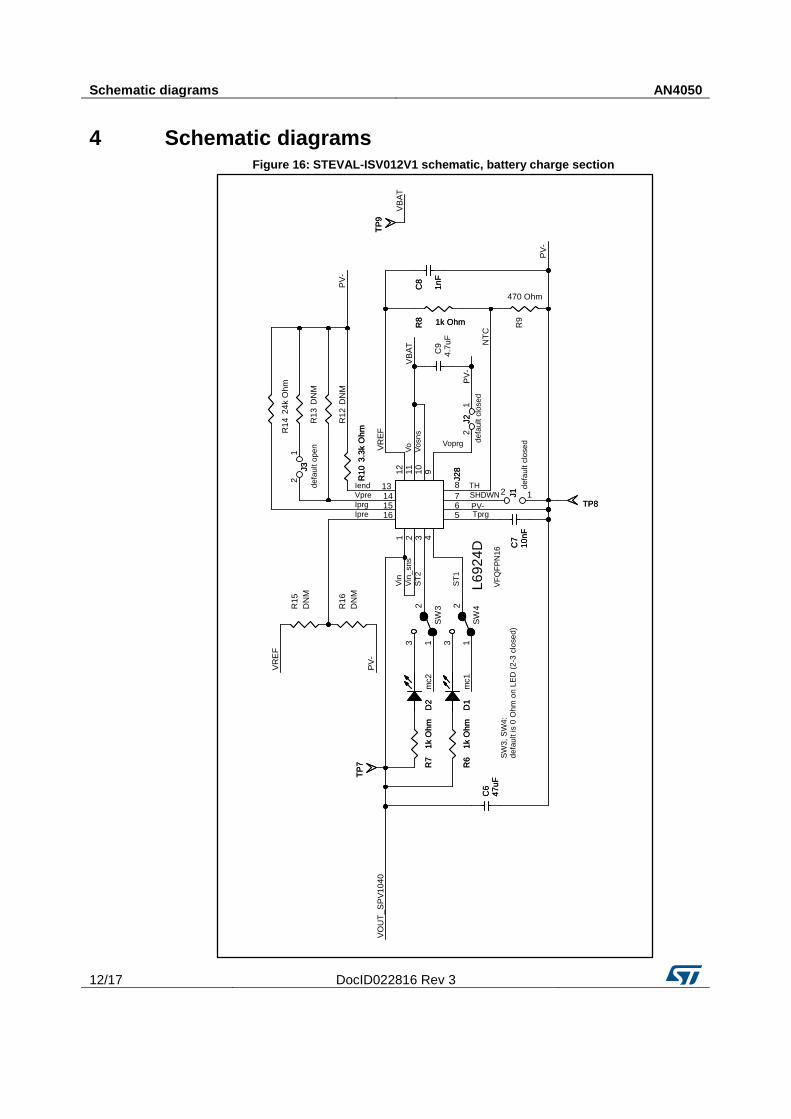
Figure 1: STEVAL-ISV012V1 evaluation board .......................................................................................... 1 Figure 2: Typical application circuit ............................................................................................................. 4 Figure 3: SPV1040 equivalent circuit .......................................................................................................... 4 Figure 4: MPPT working principle ............................................................................................................... 5 Figure 5: SPV1040 internal block diagram ................................................................................................. 5 Figure 6: Basic application schematic ........................................................................................................ 6 Figure 7: Typical charge curve in Quasi-pulse mode ................................................................................. 7 Figure 8: Battery charging at low irradiation ............................................................................................... 8 Figure 9: Battery charging at low irradiation (zoom) ................................................................................... 8 Figure 10: Maximum available current vs. Pin, 200 mW peak PV panel .................................................... 9 Figure 11: Maximum available current vs. Pin, 2 W peak PV panel ........................................................... 9 Figure 12: Application set-up .................................................................................................................... 10 Figure 13: V-I and P-V plot diagrams ....................................................................................................... 10 Figure 14: Partial charge .......................................................................................................................... 11 Figure 15: Full charge ............................................................................................................................... 11 Figure 16: STEVAL-ISV012V1 schematic, battery charge section .......................................................... 12 Figure 17: STEVAL-ISV012V1 schematic, solar power optimizer section ............................................... 13
SPV1040 operation AN4050
4/17 DocID022816 Rev 3
1 SPV1040 operation
The SPV1040 device is a low power, low voltage, monolithic step-up converter with an input voltage range from 0.3 V to 5.5 V, capable of maximizing the energy generated by a single solar cell (or fuel cell), where low input voltage handling capability is important. When combined with the L6924D, it provides an ideal solution for charging lithium battery packs with energy harvested from a very small solar panel.
The SPV1040 is a 100 kHz, fixed-frequency pulse width modulation (PWM) step-up converter able to maximize the energy harvested by a few solar cells. It employs a maximum power point tracking (MPPT) algorithm which continuously tracks its output voltage and current. The converter guarantees the safety of the overall application and its own by stopping PWM switching in case of an overvoltage, overcurrent or overtemperature condition. The IC integrates a 120 mΩ N-channel MOSFET power switch and a 140 mΩ P-channel MOSFET synchronous rectifier.
Figure 2: Typical application circuit
The SPV1040 acts as an impedance adapter between the PV module and the output load. The equivalent circuit is shown below.
Figure 3: SPV1040 equivalent circuit
The MPPT algorithm sets up the correct DC working point by ensuring Zin = Zm (assuming Zm is the impedance of the supply source). In this way, the power extracted from the supply source (Pin = Vin * Iin) is maximum (Pm = Vm * Im).
The voltage-current curve shows all the available working points of the PV panel at a given solar irradiation. The voltage-power curve is derived from the voltage-current curve by plotting the product V*I for each voltage generateda.
Figure 4: MPPT working principle
Figure 5: SPV1040 internal block diagram
The duty cycle set by the MPPT algorithm can be overwritten if one of the following events is triggered:
Input overcurrent protection (OVC): inductor peak current ≤ 1.65 A
Overtemperature protection (OVT): internal temperature ≤ 155 °C
Output voltage regulation: VCTRL pin triggers the 1.25 V internal reference
MPP-SET voltage VMPP-SET ≤ 300 mV at startup and VMPP-SET ≤ 450 mV in running mode.
Application components must be carefully selected to avoid any undesired triggering of the above thresholds.
a For more details regarding the MPPT algorithm, refer to the SPV1040 datasheet.
I MP
PMAX
[A]
[W]
urre
nt
ow
er
C P
Voltage [V]0 VOCVMP
STARTSTART SSIGNALIGNAL
Lx
XSHUT
MPP BLOCK
DETECTOR
-
Bu
rst R
ef
CLO
CK
+
-
GND
OVER CURRENT
OVER TEMPERATURE
REVERSE POLARITY
+
BURST MODE DIGITAL
DAC CODE
CORE MPP-SET
VREF
V
-
CTRL_PLUS
I
CLOCK
CTRL
V
CTRL_MINUS
MPP-REF
PWM
DR
IVE
RS
CO
NT
RO
L
MPP-SET
V
ZEROZERO CROSSINGCROSSING
OUT
V
ANALOG BLOCK
MPP-REF
I
+Iout Reg
Vin Reg
Vout Reg
VREF
+
-
L6924D operation AN4050
6/17 DocID022816 Rev 3
2 L6924D operation
The L6924D is a fully monolithic battery charger dedicated to single-cell Li-Ion/polymer battery packs. It is designed with BCD6 technology and integrates all of the power elements (Power MOSFET, reverse blocking diode and sense resistor) in a small VFQFPN16 3 mm x 3 mm package.
It normally works as a linear charger when powered from an external voltage regulated adapter. However, thanks to its very low minimum input voltage (down to 2.5 V) the L6924D can also work as a quasi-pulse charger when powered from a current limited adapter, dramatically reducing the power dissipation.
The L6924D charges the battery in three phases:
Pre-charge constant current: a deeply discharged battery is charged with a low current.
Fast-charge constant current: the device charges the battery with the maximum current.
Constant voltage: when the battery voltage is close to the selected output voltage, the device starts to reduce the current until the charge termination has completed.
Regardless of the charging approach, a closed loop thermal control features protects the device from overheating. The L6924D allows the user to program many parameters, such as pre-charge current, fast-charge current, pre-charge voltage threshold, end-of-charge current threshold and charge timer.
The L6924D offers two open collector outputs for diagnostic purposes, which can be used to either drive two external LEDs or communicate with a host microcontroller.
Finally, the L6924D also provides other battery related functions, such as checking for battery presence, monitoring and protection from unsafe thermal conditions.
Figure 6: Basic application schematic
2.1 L6924D operation in solar powered applications
Thanks to its very low minimum input voltage (down to 2.5 V), the L6924D can also work as a quasi-pulse charger when powered from a current limited adapter such as a PV panel or a current limiting device such as the SPV1040 step-up.
To work in this condition, set the device charging current (with R14) higher than the maximum peak current of the PV panel. During the fast-charge phase, the output voltage of the SPV1040 that supplies the L6924D drops down to the battery voltage plus the voltage drop across the power MOSFET of the charger.
In this mode, the L6924D charges the battery with the same three phases as in linear mode, but power dissipation is greatly reduced, as shown in the following figure.
Figure 7: Typical charge curve in Quasi-pulse mode
During the fast-charge phase, the output voltage of the SPV1040 (VIN of L6924D) drops down to the battery voltage (VBAT) plus the voltage drop across the Power MOSFET (ΔVMOS) of the charger.
Consequently, the internal MOSFET works in saturation mode with a voltage drop given by:
ILIM is the current limit of the SPV1040, which depends on solar irradiation.
Neglecting the voltage drop across the charger (ΔVMOS) when the device operates in this condition, its input voltage is equal to the battery’s, and therefore a very low operating input voltage (down to 2.5 V) is required. The power dissipated by the device during this phase is:
Equation 3
𝑃𝐶𝐻 = 𝑅𝐷𝑆(𝑜𝑛) × 𝐼𝐿𝐼𝑀2
The advantage of the quasi-pulse charging method allows the energy harvested by few solar cells to be maximized.
The STEVAL-ISV0012V1 LEDs D1 and D2 indicate (when ON) whether the charge is in progress or is completed, respectively.
R14, and consequently ILIM, must be set up according to the power provided by the PV panel at the maximum irradiation, but it is possible that D1 starts flickering (or appearing ON) at lower irradiation levels, while D2 is ON as well.
This is due to the battery charger, which tries to charge the battery at 4.2 V (or 4.1 V, depending on the VOPRG setting) and ILIM, but the required power can only be sustained if enough irradiation is available on the PV panel side. If the irradiation is not sufficient, the input voltage of the L6924D drops down to the battery voltage, causing battery charging to stop and D1 to turn ON. Shortly after, the voltage rises back to 4.2 V (or 4.1 V) and the battery charge starts again (D1 turns OFF).
In these low irradiation conditions the battery is charged by current packets anyway.
The plots below demonstrate the behavior in the event of low irradiation.
Figure 8: Battery charging at low irradiation
Figure 9: Battery charging at low irradiation (zoom)
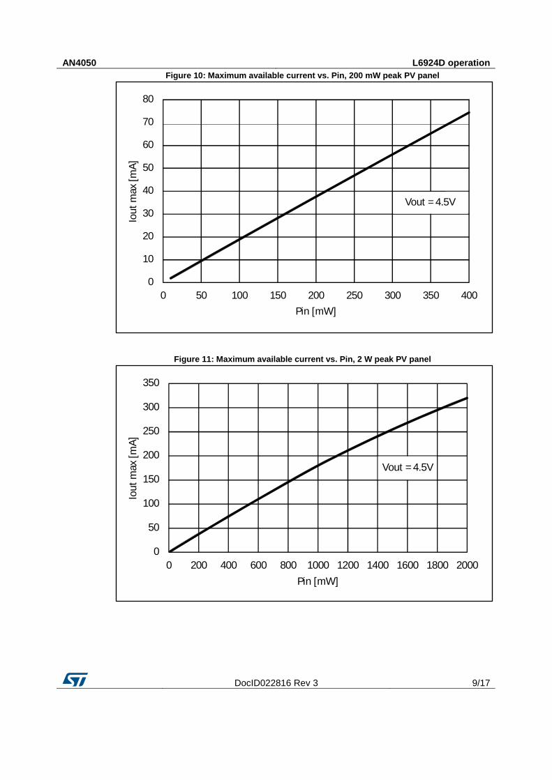
The plots below show the maximum available current that can be provided to the battery charger according to the input power.
AN4050 L6924D operation
DocID022816 Rev 3 9/17
Figure 10: Maximum available current vs. Pin, 200 mW peak PV panel
Figure 11: Maximum available current vs. Pin, 2 W peak PV panel
0
10
20
30
40
50
60
70
80
0 50 100 150 200 250 300 350 400
Pin [mW]
Iout
max
[mA
]
Vout = 4.5V
0
50
100
150
200
250
300
350
0 200 400 600 800 1000 1200 1400 1600 1800 2000
Pin [mW]
Iout
max
[mA
]
Vout = 4.5V
Reference design description AN4050
10/17 DocID022816 Rev 3
3 Reference design description
The set-up used for measurements is shown below.
Figure 12: Application set-up
A solar array simulator (SAS, SAS-FL05/01 from CBL Electronics) to simulate the PV module with VOC = 2.5 V, ISC = 210 mA, Vmp = 2.0 V, Imp = 200 mA (@ 1000 W/m² irradiance) and a Li-Ion battery 3.7 V-700 mAh, are used. Figure 13: "V-I and P-V plot diagrams" shows the I-V and P-V curves generated by the SAS, obtained using a PV module analyzer (ISM490 from ISOTECH).
Figure 13: V-I and P-V plot diagrams
Figure 14: "Partial charge" and Figure 15: "Full charge" show the partial and full charge curves respectively. The partial charge curve shows charge current and voltage within a one hour time frame at full irradiation starting from a 3.4 V condition. The full charge curve shows charge current and voltage until the fully charged status is triggered, starting from a 3.4 V condition. After the one hour charge period time, the battery voltage reaches 3.8 V.
Different results can be obtained if a different PV panel and/or battery are useda.
a Visit the support section on www.st.com if you require help regarding the use of different PV panels or batteries.
AN4050 Reference design description
DocID022816 Rev 3 11/17
The average overall power efficiency is approximately 85% (94% for SPV1040 and 90% for L6924D).
05-Dec-2017 3 Text and formatting changes throughout document.
Updated Section 5: "Bill of materials"
AN4050
DocID022816 Rev 3 17/17
IMPORTANT NOTICE – PLEASE READ CAREFULLY
STMicroelectronics NV and its subsidiaries (“ST”) reserve the right to make changes, corrections, enhancements, modifications , and improvements to ST products and/or to this document at any time without notice. Purchasers should obtain the latest relevant information on ST products before placing orders. ST products are sold pursuant to ST’s terms and conditions of sale in place at the time of order acknowledgement.
Purchasers are solely responsible for the choice, selection, and use of ST products and ST assumes no liability for application assistance or the design of Purchasers’ products.
No license, express or implied, to any intellectual property right is granted by ST herein.
Resale of ST products with provisions different from the information set forth herein shall void any warranty granted by ST for such product.
ST and the ST logo are trademarks of ST. All other product or service names are the property of their respective owners.
Information in this document supersedes and replaces information previously supplied in any prior versions of this document.