IEEE TRANSACTIONS ON NUCLEAR SCIENCE, VOL. 55, NO. 6, DECEMBER 2008 3189
Analysis of Proton and Heavy-Ion IrradiationEffects on Phase Change Memories
With MOSFET and BJT SelectorsAlberto Gasperin, Student Member, IEEE, Alessandro Paccagnella, Member, IEEE, James R. Schwank,
Gyorgy Vizkelethy, Member, IEEE, Federica Ottogalli, and Fabio Pellizzer
Abstract—We study proton and heavy ion irradiation effects onPhase Change Memories (PCM) with MOSFET and BJT selectorsand the effect of the irradiation on the retention characteristics ofthese devices. Proton irradiation produces noticeable variations inthe cell distributions in PCM with MOSFET selectors mostly due toleakage currents affecting the transistors. PCM with BJT selectorsshow only small variations after proton irradiation. PCM cells donot appear to be impacted by heavy-ion irradiation. Using hightemperature accelerated retention tests, we demonstrate that theretention capability of these memories is not compromised by theirradiation.
Index Terms—Chalcogenide material, GST, heavy ions,non-volatile memories, phase change memories (PCM), radi-ation effects.
I. INTRODUCTION
F LASH memory cell size has been progressively reducedto achieve high-density and low-cost products. However,
flash memories are now facing problems resulting from contin-uous scaling and it is not clear how they can be scaled beyondthe 45-nm technology node [1]–[4].
Among others, Phase Change Memories (PCM) [2]–[4] ap-pear to be one of the most promising candidates to replace FGNOR flash memories in the future. PCMs employ a chalco-genide material, such as Ge-Sb-Te alloy (GST), to store infor-mation. GST reversibly changes its microstructural phase be-
Manuscript received July 09, 2008; revised September 25, 2008. Current ver-sion published December 31, 2008. This work was supported in part by PRIN-MIUR, Italy, project “Memorie non volatili nanometriche a cambiamento difase”, in part by FIRB, “Tecnologie innovative per lo sviluppo di memorie nonvolatili ad alta densità”, and the Sandia portion of this work was supported by theDefense Threat Reduction Agency and the U.S. Department of Energy. Sandia isa multiprogram laboratory operated by Sandia Corporation, a Lockheed MartinCompany, for the United States Department of Energy’s National Nuclear Se-curity Administration under Contract DE-AC04-94AL85000.
A. Gasperin and A. Paccagnella are with the Dipartimento di Ingeg-neria dell’Informazione—Università di Padova, 35131 Padova, Italy, andalso with the Istituto Nazionale di Fisica Nucleare (INFN), 35131 Padova,Italy (e-mail: [email protected]; [email protected];[email protected]).
J. R. Schwank and G. Vizkelethy are with Sandia National Laborato-ries, Albuquerque, NM 87185-1083 USA (e-mail: [email protected];[email protected]).
Color versions of one or more of the figures in this paper are available onlineat http://ieeexplore.ieee.org.
Digital Object Identifier 10.1109/TNS.2008.2007639
tween amorphous and polycrystalline when properly heated andcooled. In the amorphous phase, GST features a high resistance,while the polycrystalline state is characterized by a low resis-tance value. Hence, by measuring the GST resistance it is pos-sible to determine the stored information.
PCMs feature several advantages respect to FG flash mem-ories; the most important advantage being the possibility toreduce cell dimensions making it possible to produce PCMchips with highly scaled technology nodes [2]–[4]. Further-more, PCMs allow users to program multiple bits per cell [5].
To date, several works have studied PCMs but only a fewworks have investigated the effects of irradiation on PCMs[6]–[9] and the interaction of the GST alloys with ionizingparticles. Moreover, few works have addressed the effects of ir-radiation on the circuitry of PCM chips and their consequences.
Recently, in [9], we presented results on the Total IonizingDose (TID) effects on 4-Mbit PCM chips integrated within astandard CMOS technology. PCM cells showed high robustnessagainst TID. The radiation induced variations were attributed tothe degradation of the MOSFETs used as cell selectors. How-ever, several issues still remain unanswered. First, the causes ofthe observed radiation induced variations are not completely un-derstood. Second, the effects of heavy-ion irradiation need to becarefully investigated. Finally, while semiconductor companiesare working on PCMs with BJT as cell selectors [10], [11], be-cause they may allow more aggressive scaling, previous works[6]–[9] have considered only PCM chips with MOSFET selec-tors: the radiation response of PCM chips with BJT selectorshave not been investigated.
II. AIM OF THE WORK
The purpose of this work is to analyze proton and heavy-ionirradiation effects on phase change memory arrays withMOSFET and BJT selectors, to compare their different re-sponses to irradiations and to understand the causes of theradiation-induced variations. Moreover, we study the effects ofproton irradiation on the entire chip area and on selected partsof the cell array, to evaluate separately the effects of irradiationon the cell array and on external circuitry. Finally, we evaluatethe effects of the ionizing radiation on the retention time ofPCMs through room and high temperature retention tests.
III. PHASE CHANGE MEMORIES
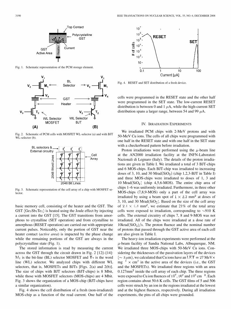
We used PCM chips produced by STMicroelectronics(Agrate, Italy) [12]–[14]. Fig. 1 shows the cross-section of the
3190 IEEE TRANSACTIONS ON NUCLEAR SCIENCE, VOL. 55, NO. 6, DECEMBER 2008
Fig. 1. Schematic representation of the PCM storage element.
Fig. 2. Schematic of PCM cells with MOSFET WL-selector (a) and with BJTWL-selector (b).
Fig. 3. Schematic representation of the cell array of a chip with MOSFET se-lector.
basic memory cell, consisting of the heater and the GST. TheGST Ge Sb Te is heated using the Joule effect by injectinga current into the GST [15]. The GST transitions from amor-phous to crystalline (SET operation) and from crystalline toamorphous (RESET operation) are carried out with appropriatecurrent pulses. Noticeably, only the portion of GST near theheater contact (active area) is impacted by the phase changewhile the remaining portions of the GST are always in thepolycrystalline state (Fig. 1).
The stored information is read by measuring the currentacross the GST through the circuit drawn in Fig. 2 [12]–[14]:
is the bit-line (BL) selector MOSFET and is the wordline (WL) selector. We analyzed chips with different WLselectors, that is, MOSFETs and BJTs [Figs. 2(a) and 2(b)].The size of chips with BJT selectors (BJT-chips) is 8 Mbit,while those with MOSFET selectors (MOS-chips) are 4 Mbit.Fig. 3 shows the organization of a MOS-chip (BJT-chips havea similar organization).
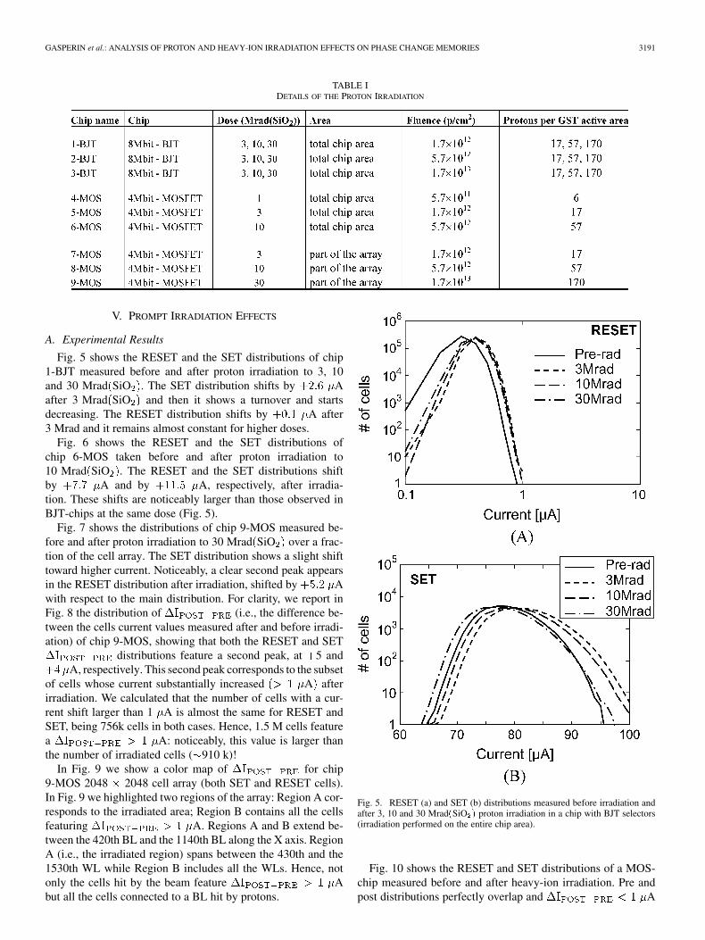
Fig. 4 shows the cell distribution of a fresh (non-irradiated)MOS-chip as a function of the read current. One half of the
Fig. 4. RESET and SET distribution of a fresh device.
cells were programmed in the RESET state and the other halfwere programmed in the SET state. The low-current RESETdistribution is between 0 and 1 A, while the high-current SETdistribution spans a larger range, between 54 and 99 A.
IV. IRRADIATION EXPERIMENTS
We irradiated PCM chips with 2-MeV protons and with50-MeV Cu ions. The cells of all chips were programmed withone half in the RESET state and with one half in the SET statewith a checkerboard pattern before irradiation.
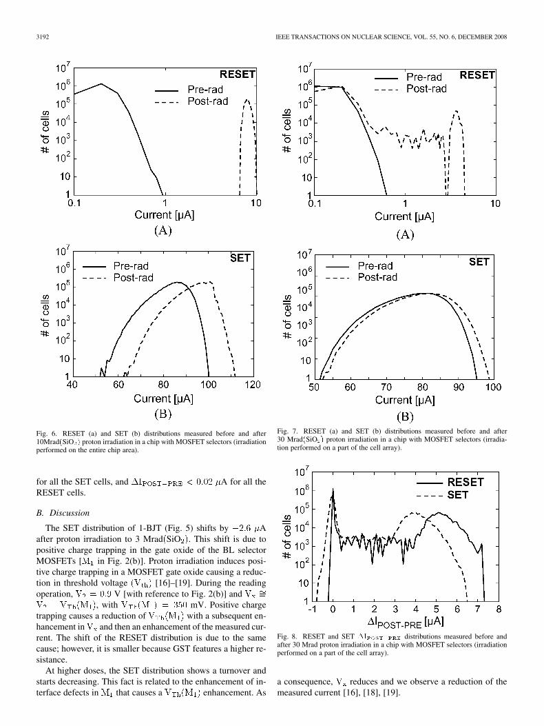
Proton irradiations were performed using the -beam lineat the AN2000 irradiation facility at the INFN-LaboratoriNazionali di Legnaro (Italy). The details of the proton irradia-tions are given in Table I. We irradiated a total of 3 BJT-chipsand 6 MOS-chips. Each BJT-chip was irradiated to increasingdoses of 3, 10, and 30 Mrad SiO (chip 1,2,3-BJT in Table I)and three MOS-chips were irradiated to doses of 1, 3 and10 Mrad SiO (chip 4,5,6-MOS). The entire chip area ofchips 1–6 was uniformly irradiated. Furthermore, in three otherMOS-chips (7,8,9-MOS) only a part of the cell array wasirradiated by using a beam spot of mm at doses of3, 10, and 30 Mrad SiO . Based on the size of the cell arrayof mm , we estimate that 21% of the total arraycells were exposed to irradiation, corresponding to 910 Kcells. The external circuitry of chips 7, 8 and 9-MOS was notirradiated. All of the chips were irradiated at a dose rate of10krad SiO s. The proton fluence and the nominal numberof protons that passed through the GST active area of each cellare also given in Table I.
The heavy-ion irradiation experiments were performed at the-beam facility of Sandia National Labs, Albuquerque, NM.
We irradiated three MOS-chips with 50-MeV Cu ions. Con-sidering the thicknesses of the passivation layers of the devices
m , we calculated that Cu ions have an MeVmg cm in the active area of the devices (i.e., the GSTand the MOSFETs). We irradiated three regions with an area0.127mm inside the cell array of each chip. The three regionswere exposed to Cu ion fluences of , and cm . Eachregion contains about 50.6 K cells. The GST films of 5 and 506cells were struck by an ion in the regions irradiated at the lowestand at the highest fluences, respectively. During all irradiationexperiments, the pins of all chips were grounded.
GASPERIN et al.: ANALYSIS OF PROTON AND HEAVY-ION IRRADIATION EFFECTS ON PHASE CHANGE MEMORIES 3191
TABLE IDETAILS OF THE PROTON IRRADIATION
V. PROMPT IRRADIATION EFFECTS
A. Experimental Results
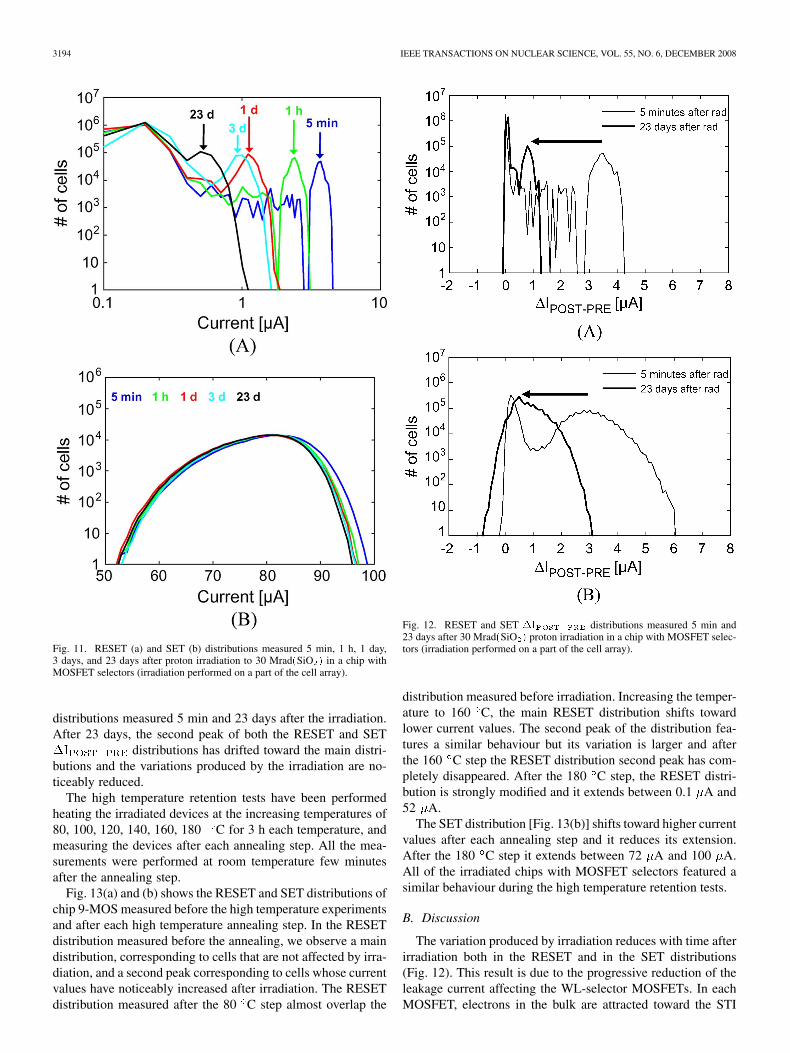
Fig. 5 shows the RESET and the SET distributions of chip1-BJT measured before and after proton irradiation to 3, 10and 30 Mrad SiO . The SET distribution shifts by Aafter 3 Mrad SiO and then it shows a turnover and startsdecreasing. The RESET distribution shifts by A after3 Mrad and it remains almost constant for higher doses.
Fig. 6 shows the RESET and the SET distributions ofchip 6-MOS taken before and after proton irradiation to10 Mrad SiO . The RESET and the SET distributions shiftby A and by A, respectively, after irradia-tion. These shifts are noticeably larger than those observed inBJT-chips at the same dose (Fig. 5).
Fig. 7 shows the distributions of chip 9-MOS measured be-fore and after proton irradiation to 30 Mrad SiO over a frac-tion of the cell array. The SET distribution shows a slight shifttoward higher current. Noticeably, a clear second peak appearsin the RESET distribution after irradiation, shifted by Awith respect to the main distribution. For clarity, we report inFig. 8 the distribution of (i.e., the difference be-tween the cells current values measured after and before irradi-ation) of chip 9-MOS, showing that both the RESET and SET
distributions feature a second peak, at 5 andA, respectively. This second peak corresponds to the subset
of cells whose current substantially increased A afterirradiation. We calculated that the number of cells with a cur-rent shift larger than 1 A is almost the same for RESET andSET, being 756k cells in both cases. Hence, 1.5 M cells featurea A: noticeably, this value is larger thanthe number of irradiated cells ( 910 k)!
In Fig. 9 we show a color map of for chip9-MOS 2048 2048 cell array (both SET and RESET cells).In Fig. 9 we highlighted two regions of the array: Region A cor-responds to the irradiated area; Region B contains all the cellsfeaturing A. Regions A and B extend be-tween the 420th BL and the 1140th BL along the X axis. RegionA (i.e., the irradiated region) spans between the 430th and the1530th WL while Region B includes all the WLs. Hence, notonly the cells hit by the beam feature Abut all the cells connected to a BL hit by protons.
Fig. 5. RESET (a) and SET (b) distributions measured before irradiation andafter 3, 10 and 30 Mrad�SiO � proton irradiation in a chip with BJT selectors(irradiation performed on the entire chip area).
Fig. 10 shows the RESET and SET distributions of a MOS-chip measured before and after heavy-ion irradiation. Pre andpost distributions perfectly overlap and A
3192 IEEE TRANSACTIONS ON NUCLEAR SCIENCE, VOL. 55, NO. 6, DECEMBER 2008
Fig. 6. RESET (a) and SET (b) distributions measured before and after10Mrad�SiO � proton irradiation in a chip with MOSFET selectors (irradiationperformed on the entire chip area).
for all the SET cells, and A for all theRESET cells.
B. Discussion
The SET distribution of 1-BJT (Fig. 5) shifts by Aafter proton irradiation to 3 Mrad SiO . This shift is due topositive charge trapping in the gate oxide of the BL selectorMOSFETs [ in Fig. 2(b)]. Proton irradiation induces posi-tive charge trapping in a MOSFET gate oxide causing a reduc-tion in threshold voltage [16]–[19]. During the readingoperation, V [with reference to Fig. 2(b)] and
, with mV. Positive chargetrapping causes a reduction of with a subsequent en-hancement in and then an enhancement of the measured cur-rent. The shift of the RESET distribution is due to the samecause; however, it is smaller because GST features a higher re-sistance.
At higher doses, the SET distribution shows a turnover andstarts decreasing. This fact is related to the enhancement of in-terface defects in that causes a enhancement. As
Fig. 7. RESET (a) and SET (b) distributions measured before and after30 Mrad�SiO � proton irradiation in a chip with MOSFET selectors (irradia-tion performed on a part of the cell array).
Fig. 8. RESET and SET �� distributions measured before andafter 30 Mrad proton irradiation in a chip with MOSFET selectors (irradiationperformed on a part of the cell array).
a consequence, reduces and we observe a reduction of themeasured current [16], [18], [19].
GASPERIN et al.: ANALYSIS OF PROTON AND HEAVY-ION IRRADIATION EFFECTS ON PHASE CHANGE MEMORIES 3193
Fig. 9. Color map of the �� value of the cells of a MOS-chip arrayirradiated with protons to 30 Mrad�SiO �. Region A indicates the irradiated areaand Region B indicates the region where cells feature �� � � �A.
Fig. 10. RESET (a) and SET (b) distributions measured before and afterheavy-ion irradiation in a chip with MOSFET selectors.
Comparing Figs. 5 and 6, we observe that the distributions ofMOS-chips feature larger shifts after irradiation. In particular,
the average current of the RESET distribution increases from0.2 to 7.9 A (Fig. 6).
The causes of this shift can be determined from the irradia-tion results of chip 9-MOS (Figs. 7–9). Only a fraction of thechip 9-MOS cell array was irradiated: hence the shift observedin Figs. 7 and 8 is not due to positive charge trapping in the gateoxide of BL-selector MOSFETs that were not irradiated. Sec-ondly, not only the irradiated cells feature a large shift Abut all of the RESET or SET cells connected to the same BL ofthe irradiated cells (Fig. 9).
The shift of the MOS-chip distributions is due to leakagecurrents affecting all of the irradiated cells connected at thesame BL. This leakage is attributable to radiation-induced pos-itive charge trapping in the Shallow Trench Insulation (STI) ofthe MOSFETs. The positive charge forms a parasitic transistorthat drives the off-state leakage current [19]–[21]. During thereading of a cell, the leakage currents of all of the irradiatedcells connected to the same BL affect the measured current.
The shift of the second peak of Fig. 7 A , is due tothe leakage currents of 1100 cells and then the leakage currentthat affects a single BL-selector MOSFET is 5 nA. This valueagrees with data in the literature [19].
It is important to note that the leakage currents and the dis-tribution shifts are not due to a modification of the GST resis-tance. In fact, during the read operation, all of the WL-selectorMOSFETs (except the one of the cell being read) are in the offstate, and their “equivalent resistance” is higher than the GSTresistance (equal to and k in the amorphousand in the crystalline state, respectively). Hence the current thatflows through a not-selected cell is controlled exclusively by theWL-selector MOSFET and a variation of the GST resistancewould have no effect on the measured current.
The results of Fig. 10 indicate that PCMs with MOSFET se-lectors are robust against high-LET particle irradiation. In fact,heavy ions do not produce much charge trapping and for thisreason, we do not observe any modification of the cell distribu-tions. Moreover, the functionality of the SET/RESET operationsis not compromised by the high-LET particle irradiation.
VI. RETENTION TESTS
A. Experimental Results
To determine if ionizing particles could compromise the re-tention characteristics of PCM cells, we performed retentiontests both at room and high temperature. The room temperatureretention tests were performed by measuring the devices severaltimes after irradiation, storing the devices floating at room tem-perature between two different measurements.
Fig. 11(a) and (b) show the RESET and the SET distributionsof chip 9-MOS measured 5 min after the irradiation and then1 h, 1 day, 3 days and 23 days after the irradiation. In the RESETdistribution, the second peak produced by irradiation drifts to-ward lower current values with time and the cells featuring alarge shift after the irradiation drift toward the main distribu-tion. The variations observed in the SET distribution are less no-ticeable due to the large span of the main SET distribution. Forclarity, we report in Fig. 12 the RESET and SET
3194 IEEE TRANSACTIONS ON NUCLEAR SCIENCE, VOL. 55, NO. 6, DECEMBER 2008
Fig. 11. RESET (a) and SET (b) distributions measured 5 min, 1 h, 1 day,3 days, and 23 days after proton irradiation to 30 Mrad�SiO � in a chip withMOSFET selectors (irradiation performed on a part of the cell array).
distributions measured 5 min and 23 days after the irradiation.After 23 days, the second peak of both the RESET and SET
distributions has drifted toward the main distri-butions and the variations produced by the irradiation are no-ticeably reduced.
The high temperature retention tests have been performedheating the irradiated devices at the increasing temperatures of80, 100, 120, 140, 160, 180 C for 3 h each temperature, andmeasuring the devices after each annealing step. All the mea-surements were performed at room temperature few minutesafter the annealing step.
Fig. 13(a) and (b) shows the RESET and SET distributions ofchip 9-MOS measured before the high temperature experimentsand after each high temperature annealing step. In the RESETdistribution measured before the annealing, we observe a maindistribution, corresponding to cells that are not affected by irra-diation, and a second peak corresponding to cells whose currentvalues have noticeably increased after irradiation. The RESETdistribution measured after the 80 C step almost overlap the
Fig. 12. RESET and SET �� distributions measured 5 min and23 days after 30 Mrad�SiO � proton irradiation in a chip with MOSFET selec-tors (irradiation performed on a part of the cell array).
distribution measured before irradiation. Increasing the temper-ature to 160 C, the main RESET distribution shifts towardlower current values. The second peak of the distribution fea-tures a similar behaviour but its variation is larger and afterthe 160 C step the RESET distribution second peak has com-pletely disappeared. After the 180 C step, the RESET distri-bution is strongly modified and it extends between 0.1 A and52 A.
The SET distribution [Fig. 13(b)] shifts toward higher currentvalues after each annealing step and it reduces its extension.After the 180 C step it extends between 72 A and 100 A.All of the irradiated chips with MOSFET selectors featured asimilar behaviour during the high temperature retention tests.
B. Discussion
The variation produced by irradiation reduces with time afterirradiation both in the RESET and in the SET distributions(Fig. 12). This result is due to the progressive reduction of theleakage current affecting the WL-selector MOSFETs. In eachMOSFET, electrons in the bulk are attracted toward the STI
GASPERIN et al.: ANALYSIS OF PROTON AND HEAVY-ION IRRADIATION EFFECTS ON PHASE CHANGE MEMORIES 3195
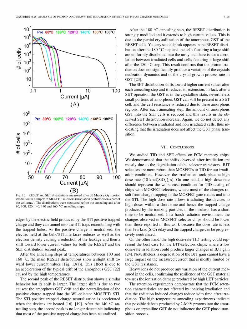
Fig. 13. RESET and SET distributions measured after 30 Mrad�SiO � protonirradiation in a chip with MOSFET selectors (irradiation performed on a part ofthe cell array). The distributions were measured before the annealing and after80, 100, 120, 140, 140 and 160 C annealing steps.
edges by the electric field produced by the STI positive trappedcharge and they can tunnel into the STI traps recombining withthe trapped holes. As the positive charge is neutralized, theelectric field at the bulk/STI interfaces reduces as well as theelectron density causing a reduction of the leakage and then ashift toward lower current values for both the RESET and theSET distribution second peak.
After the annealing steps at temperatures between 100 and160 C, the main RESET distributions show a slight shift to-ward lower current values [Fig. 13(a)]. This effect is due toan acceleration of the typical drift of the amorphous GST [22]caused by the high temperatures.
The second peak of the RESET distribution shows a similarbehavior but its shift is larger. The larger shift is due to twocauses: the amorphous GST drift and the neutralization of thepositive charge trapped into the WL-selector MOSFETs STI.The STI positive trapped charge neutralization is acceleratedwhen the devices are heated [16], [19]. After the 140 C an-nealing step, the second peak is no longer detectable indicatingthat most of the positive trapped charge has been neutralized.
After the 180 C annealing step, the RESET distribution isstrongly modified and it extends to high current values. This isdue to the partial crystallization of the amorphous GST of theRESET cells. Yet, any second peak appears in the RESET distri-bution after the 180 C step and the cells featuring a large shiftare uniformly distributed into the array and there is not a corre-lation between irradiated cells and cells featuring a large shiftafter the 180 C step. This result confirms that the proton irra-diation does not significantly produce a variation of the crystalsnucleation dynamics and of the crystal growth process rate inGST [23].
The SET distribution shifts toward higher current values aftereach annealing step and it reduces its extension. In fact, after aSET operation the GST is in the crystalline state, neverthelesssmall portions of amorphous GST can still be present in a SETcell, and the cell resistance is reduced due to these amorphousregions. After each annealing step, the amount of amorphousGST into the SET cells is reduced and this results in the ob-served SET distribution increase. Again, we do not detect anydifference between irradiated and non irradiated cells, thus in-dicating that the irradiation does not affect the GST phase tran-sition.
VII. CONCLUSIONS
We studied TID and SEE effects on PCM memory chips.We demonstrated that the shifts observed after irradiation aremostly due to the degradation of the selector transistors. BJTselectors are more robust than MOSFETs to TID for our irradi-ation conditions. However, the irradiations took place at highdose rate (10 krad SiO s). On one hand, a high dose rateshould represent the worst case condition for TID testing ofchips with MOSFET selectors, where most of the changes re-sult from charge trapping in the MOSFET gate oxides and intothe STI. The high dose rate allows irradiating the devices tohigh doses within a short time and hence the trapped chargeproduced by the ionizing particles in the insulator has a shorttime to be neutralized. In a harsh radiation environment thechanges observed in MOSFET selector chips should be lowerthan those reported in this work because the dose rate is lessthan few krad SiO /day and the trapped charge can be progres-sively neutralized.
On the other hand, the high dose-rate TID testing could rep-resent the best case for the BJT-selectors chips, where a lowdose-rate irradiation could produce larger changes in BJT gain[24]. Nevertheless, a degradation of the BJT gain cannot have alarge impact on the measured current that is mostly limited bythe GST resistance.
Heavy ions do not produce any variation of the current mea-sured in the cells, confirming the resilience of the GST materialtowards the ionization damage produced by high LET particles.
The retention experiments demonstrate that the PCM reten-tion characteristics are not affected by ionizing irradiation andthat the radiation induced changes reduce with time after irra-diation. The high temperature annealing experiments indicatethat possible defects produced by 2-MeV protons into the amor-phous or crystalline GST do not influence the GST phase-tran-sition process.
3196 IEEE TRANSACTIONS ON NUCLEAR SCIENCE, VOL. 55, NO. 6, DECEMBER 2008
In conclusion, GST does not appear to be highly affected byionizing particles. However, 2-MeV protons and 50-MeV Cuions loose most of their energy through ionizing processes inthe first few microns of the chip (where there are the GST andthe transistors) and only in the bulk of the device such particlesdeposit energy through non-ionizing processes. The effect ofthe interaction between high energy particles and GST throughnon-ionizing processes could produce structural modificationsof the GST alloy and this needs to be further investigated.
REFERENCES
[1] R. Bez and A. Pirovano, “Non-volatile memory technologies:Emerging concepts and new materials,” Mat. Sci. Semic. Process., vol.7, pp. 349–355, 2004.
[2] A. Pirovano, A. L. Lacaita, A. Benvenuti, F. Pellizzer, S. Hudgens,and R. Bez, “Scaling analysis of phase-change memory technology,”in IEDM Tech. Dig., 2003, p. 699.
[3] R. Bez and G. Atwood, “Chalcogenide phase change memory: ScalableNVM for the next decade?,” in Proc. IEEE 21st NVSMW, 2006, p. 12.
[4] A. Pirovano, A. Redaelli, F. Pellizzer, F. Ottogalli, M. Tosi, D. Ielmini,A. L. Lacaita, and R. Bez, “Reliability study of phase-change non-volatile memories,” IEEE Trans. Dev. Mater. Rel., vol. 4, p. 422, 2004.
[5] F. Bedeschi, R. Fackenthal, C. Resta, E. M. Donze, M. Jagasivamani,E. Buda, F. Pellizzer, D. Chow, A. Cabrini, G. M. A. Calvi, R. Far-avelli, A. Fantini, G. Torelli, D. Mills, R. Gastaldi, and G. Casagrande,“A multi-level-cell bipolar-selected phase-change memory,” in Proc.ISSCC, Dig. Tech. Papers, 2008, pp. 428–429.
[6] S. Bernacki, K. Hunt, S. Tyson, S. Hudgens, B. Pashmakov, and W.Czubatyj, “Total dose radiation response and high temperature imprintcharacteristics of chalcogenide based RAM resistor elements,” IEEETrans. Nucl. Sci., vol. 47, no. 6, pp. 2528–2533, Dec. 2000.
[7] J. D. Maimon, K. Hunt, L. Burcin, and J. Rodgers, “Chalcogenidememory arrays: Characterization and radiation effects,” IEEE Trans.Nucl. Sci., vol. 50, no. 6, pp. 1878–1884, Dec. 2003.
[8] J. D. Maimon, K. Hunt, J. Rodgers, L. Burcin, and K. Knowles, “Re-sults of radiation effects on a chalcogenide non-volatile memory array,”in Proc. IEEE Aerospace Conf., Mar. 2004, vol. 4, pp. 2306–2315.
[9] A. Gasperin, N. Wrachien, A. Paccagnella, F. Ottogalli, U. Corda, P.Fuochi, and M. Lavalle, “Total ionizing dose effects on 4 Mbit phasechange memory arrays,” IEEE Trans. Nucl. Sci., to be published.
[10] K. J. Lee, B. H. Cho, W. Y. Cho, S. Kang, B. G. Choi, H. R. Oh, C. S.Lee, H. J. Kim, J. M. Park, Q. Wang, M. H. Park, Y. H. Ro, J. Y. Choi,K. S. Kim, Y. R. Kim, I. C. Shin, K. W. Lim, H. K. Cho, C. H. Choi, W.R. Chung, D. E. Kim, K. S. Yu, G. T. Jeong, H. S. Jeong, C. K. Kwak,C. H. Kim, and K. Kim, “A 90 nm 1.8 V 512 Mb diode-switch PRAMwith 266 MB/s read throughput,” in Proc. ISSCC, Dig. Tech. Papers,,2007, pp. 472–473.
[11] F. Pellizzer, A. Benvenuti, B. Gleixner, Y. Kim, B. Johnson, M. Mag-istretti, T. Marangon, A. Pirovano, R. Bez, and G. Atwood, “A 90 nmphase change memory technology for stand-alone non-volatile memoryapplications,” in Proc. Symp. VLSI Technology, 2006, pp. 122–123.
[12] F. Bedeschi, R. Bez, C. Boffino, E. Bonizzoni, Buda, G. Casagrande, L.Costa, M. Ferraro, R. Gastaldi, O. Khouri, F. Ottogalli, F. Pellizzer, A.Pirovano, C. Resta, G. Torelli, and M. Tosi, “4-Mb MOSFET-selectedphase-change memory experimental chip,” in Proc. IEEE ESSCIRC,2004, p. 207.
[13] F. Bedeschi, R. Bez, C. Boffino, E. Bonizzoni, E. C. Buda, G.Casagrande, L. Costa, M. Ferraro, R. Gastaldi, O. Khouri, F. Ottogalli,F. Pellizzer, A. Pirovano, C. Resta, G. Torelli, and M. Tosi, “4-MbMOSFET-selected � trench phase-change memory experimentalchip,” IEEE J. Solid-State Circuits, vol. 40, p. 1557, 2005.
[14] F. Bedeschi, C. Resta, O. Khouri, E. Buda, L. Costa, M. Ferraro, F.Pellizzer, F. Ottogalli, A. Pirovano, M. Tosi, R. Bez, R. Gastaldi, andG. Casagrande, “An 8 Mb demonstrator for high-density 1.8 V phase-change memories,” in Proc. VLSI Circuits Dig. Tech. Papers, 2004, p.442.
[15] F. Pellizzer, A. Pirovano, F. Ottogalli, M. Magistretti, M. Scaravaggi,P. Zuliani, M. Tosi, A. Benvenuti, P. Besana, S. Cadeo, T. Marangon,R. Morandi, R. Piva, A. Spandre, R. Zonca, A. Modelli, E. Varesi, T.Lowrey, A. Lacaita, G. Casagrande, P. Cappelletti, and R. Bez, “Novel�-trench phase-change memory cell for embedded and stand-alonenon-volatile memory applications,” in Proc. VLSI Tech. Dig., 2004, p.18.
[16] J. Schwank, “Total dose effects in MOS devices,” presented at the IEEENSREC Short Courses, 2002.
[17] A. Paccagnella and A. Cester, “Radiation response and reliability ofoxide used in advanced processes,” presented at the IEEE NSRECShort Courses, 2003.
[18] M. Manghisoni, L. Ratti, V. Re, and V. Speziali, “Radiation hardnessperspectives for the design of analog detector readout circuits in the0.18-�m CMOS generation,” IEEE Trans. Nucl. Sci., vol. 49, no. 6,pp. 2902–2909, Dec. 2002.
[19] F. Faccio and G. Cervelli, “Radiation-induced edge effects in deep sub-micron CMOS transistor,” IEEE Trans. Nucl. Sci., vol. 52, no. 6, pp.2413–2420, Dec. 2005.
[20] M. R. Shaneyfelt, P. E. Dodd, P. E. B. L. Draper, and R. S. Flores,“Challenges in hardening technologies using shallow-trench isolation,”IEEE Trans. Nucl. Sci., vol. 45, no. 6, pp. 2584–2592, Dec. 1998.
[21] M. Turowski, A. Raman, and R. D. Schrimpf, “Nonuniform total-dose-induced charge distribution in shallow-trench isolation oxide,” IEEETrans. Nucl. Sci., vol. 51, no. 6, pp. 3166–3171, Dec. 2004.
[22] A. Pirovano, A. L. Lacaita, F. Pellizzer, S. A. Kostylev, A. Benvenuti,and R. Bez, “Low-field amorphous state resistance and thresholdvoltage drift in chalcogenide materials,” IEEE Trans. Electron. De-vices, vol. 51, p. 714, 2004.
[23] S. Privitera, C. Bongiorno, E. Rimini, and R. Zonca, “Crystal nucle-ation and growth processes in Ge2Sb2Te5,” Appl. Phys. Lett., vol. 80,p. 4448, 2004.
[24] R. D. Schrimpf, “Physics and hardness assurance for bipolar technolo-gies,” presented at the IEEE NSREC Short Courses, 2001.