Analytical model for the AIGaAs/GaAs multiemitter finger HBT including self-heating and thermal coupling effects J.J. Liou L.L. Liou C.I. Huang Indexing terms: Heterojunction bipolar transistcr, Semiconductor device modelling Abstract: An analytical model which can be used to predict the thermal as well as electronic behav- iour of the multiple emitter hererojunction bipolar transistor (HBT) is presented. The model is devel- oped from a knowledge of device make-up (doping concentrations, layer thicknesses etc.), and relevant physics (such as the effects of graded het- erojunction, self-heating, thermal coupling and ballast emitter resistance) is included in a unified manner. Thermal runaway phenomenon observed in the multifinger HBT at high current levels has been successfully described. Experimental evidence obtained from six-finger and four-finger HBTs are included in support of the model. The thermal runaway phenomenon is caused by the uneven increase of the base and collector currents at ele- vated temperatures due to the thermal effect. 1 Introduction The advance of AlGaAs/GaAs heterojunction bipolar transistor (HBT) technology in recent years has made high output power possible and practical. The HBTs very high current handling capability and the very poor thermal conductivity of GaAs, however, often lead to a significant self-heating effect which confines the HBT per- formance considerably below its electronic limitation, as reviewed in Reference 1. For modern microwave HBTs, a multiple emitter finger structure has frequently been used, in which several HBT emitters, each with its own HBT operation, are arranged in parallel to each other with proper spacing [2]. Such a structure can reduce the HBT signal propagation delay time. In addition, it allows less current to be carried and thus less heat power to be gen- erated in each HBT unit cell, thus making the self-heating effect less prominent compared to its single-emitter finger counterpart. Recently, a 12.5 W cw (emitter area power density: 1.74 mW/pm2) monolithic amplifier constructed using 12-finger HBTs was demonstrated at 10 GHz [3]. 0 IEE, 1994 Paper 13946 (E3), first received 17th December 1993 and in revised form 28th April 1994 J.J. Liou is with the Electrical and Computer Engineering Department, University of Central Florida, Orlando, FL 32816, USA L.L. Liou and C.1. Huang are with the Solid-state Electronics Direc- torate, Wright Laboratory, Wright-Patterson AFB, OH 45433, USA IEE Proc.-Circuits Devices Syst., Vol. 141, No. 6, December 1994 Although the multifinger HBT offers higher output power density, it is more susceptible to a thermally limited phenomenon called thermal runaway [4]. When the base current is fixed and is relatively large, the collec- tor current decreases sharply (thermal runaway) as the collector+mitter voltage is increased beyond a critical value. This phenomenon results from the combination of self-heating in the unit emitter finger and thermal coup- ling among the neighbouring fingers. A common remedy to this problem is to use large resistors (ballast resistors) at the emitter and/or base contacts [SI. Such a resistance gives rise to a large voltage drop at the contact and thus reduces the voltage drop across the emitter-base junc- tion. This in turn decreases the current density and the heat generated in each unit HBT. Evidently, this approach limits the output power density, not by thermal, but by electronic means. It can also degrade the HBT high frequency performance due to the extra delay time through the ballast resistance. Despite the fact that the multifinger HBT has become increasingly important and popular in high-power micro- wave applications, efforts on analytical modelling of such a device have been limited in the past. This is due in part to the complicated nature of the negative feedback of the thermal effect on the HBT current-voltage character- istics. The problem is further compounded by the thermal coupling between the neighbouring emitter fingers when a multifinger structure is considered. A few numerical models have been reported in the literature [4, 6-83. For example, solving the three-dimensional heat transfer equation, Gao et al. [6] studied the temperature in each emitter finger as a function of the emitter spacing, the number of the fingers, and the geometry of the substrate. Their results, however, are not directly suited for HBT design because the heat power on each finger, which is related to the current and applied voltage, was treated as an independent input parameter. A self-consistent two- dimensional model was also developed by Marty et al. [SI to investigate the coupled electrothermal problem in AlGaAs/GaAs HBTs. In this approach, the current and temperature variations in the HBT are computed by con- sidering a series of cells within the device, and the 2D the Initiation Grant (account 16-22-502) and Summer Faculty Program (1993) funded by the Air Force Ofice of Scientific Research. 469
Transcript
Analytical model for the AIGaAs/GaAs multiemitter finger HBT including self-heating and thermal coupling effects
Abstract: An analytical model which can be used to predict the thermal as well as electronic behav- iour of the multiple emitter hererojunction bipolar transistor (HBT) is presented. The model is devel- oped from a knowledge of device make-up (doping concentrations, layer thicknesses etc.), and relevant physics (such as the effects of graded het- erojunction, self-heating, thermal coupling and ballast emitter resistance) is included in a unified manner. Thermal runaway phenomenon observed in the multifinger HBT at high current levels has been successfully described. Experimental evidence obtained from six-finger and four-finger HBTs are included in support of the model. The thermal runaway phenomenon is caused by the uneven increase of the base and collector currents at ele- vated temperatures due to the thermal effect.
1 Introduction
The advance of AlGaAs/GaAs heterojunction bipolar transistor (HBT) technology in recent years has made high output power possible and practical. The HBTs very high current handling capability and the very poor thermal conductivity of GaAs, however, often lead to a significant self-heating effect which confines the HBT per- formance considerably below its electronic limitation, as reviewed in Reference 1. For modern microwave HBTs, a multiple emitter finger structure has frequently been used, in which several HBT emitters, each with its own HBT operation, are arranged in parallel to each other with proper spacing [2]. Such a structure can reduce the HBT signal propagation delay time. In addition, it allows less current to be carried and thus less heat power to be gen- erated in each HBT unit cell, thus making the self-heating effect less prominent compared to its single-emitter finger counterpart. Recently, a 12.5 W cw (emitter area power density: 1.74 mW/pm2) monolithic amplifier constructed using 12-finger HBTs was demonstrated at 10 GHz [3].
0 IEE, 1994 Paper 13946 (E3), first received 17th December 1993 and in revised form 28th April 1994 J.J. Liou is with the Electrical and Computer Engineering Department, University of Central Florida, Orlando, FL 32816, USA L.L. Liou and C.1. Huang are with the Solid-state Electronics Direc- torate, Wright Laboratory, Wright-Patterson AFB, OH 45433, USA
I E E Proc.-Circuits Devices Syst., Vol. 141, No. 6, December 1994
Although the multifinger HBT offers higher output power density, it is more susceptible to a thermally limited phenomenon called thermal runaway [4]. When the base current is fixed and is relatively large, the collec- tor current decreases sharply (thermal runaway) as the collector+mitter voltage is increased beyond a critical value. This phenomenon results from the combination of self-heating in the unit emitter finger and thermal coup- ling among the neighbouring fingers. A common remedy to this problem is to use large resistors (ballast resistors) at the emitter and/or base contacts [SI. Such a resistance gives rise to a large voltage drop at the contact and thus reduces the voltage drop across the emitter-base junc- tion. This in turn decreases the current density and the heat generated in each unit HBT. Evidently, this approach limits the output power density, not by thermal, but by electronic means. It can also degrade the HBT high frequency performance due to the extra delay time through the ballast resistance.
Despite the fact that the multifinger HBT has become increasingly important and popular in high-power micro- wave applications, efforts on analytical modelling of such a device have been limited in the past. This is due in part to the complicated nature of the negative feedback of the thermal effect on the HBT current-voltage character- istics. The problem is further compounded by the thermal coupling between the neighbouring emitter fingers when a multifinger structure is considered. A few numerical models have been reported in the literature [4, 6-83. For example, solving the three-dimensional heat transfer equation, Gao et al. [6] studied the temperature in each emitter finger as a function of the emitter spacing, the number of the fingers, and the geometry of the substrate. Their results, however, are not directly suited for HBT design because the heat power on each finger, which is related to the current and applied voltage, was treated as an independent input parameter. A self-consistent two- dimensional model was also developed by Marty et al. [SI to investigate the coupled electrothermal problem in AlGaAs/GaAs HBTs. In this approach, the current and temperature variations in the HBT are computed by con- sidering a series of cells within the device, and the 2D
the Initiation Grant (account 16-22-502) and Summer Faculty Program (1993) funded by the Air Force Ofice of Scientific Research.
469
heat transfer in the HBT is represented by an electrical circuit analog involving vertical and horizontal thermal resistances. Such an equivalent circuit is then incorpor- ated into a circuit simulator to simulate the HBT per- formance. The model, however, is limited to single-emitter finger HBTs and requires the use of a circuit simulator. Recently, an analytical HBT model including the self-heating effect was derived from the knowledge of HBT make-up [SI, but it again is only applicable for the single-finger HBT. Furthermore, the model employs the driftdiffusion theory for the charge transport in the HBT, an approximation valid only for HBTs having an ideal graded heterojunction [lo].
This paper develops a physics-based and analytical model capable of predicting the multifinger HBT current-voltage characteristics. Relevant physics such as the effects of self-heating, thermal coupling between fingers, ballast emitter resistance will be accounted for in a unified manner. In addition, the model accounts for the thermionic and tunnelling mechanisms at the hetero- interface and is applicable for HBTs having a nonideal graded heterojunction.
2 HBT model development
2.1 Band structure and barrier porenrials of graded heterojunction
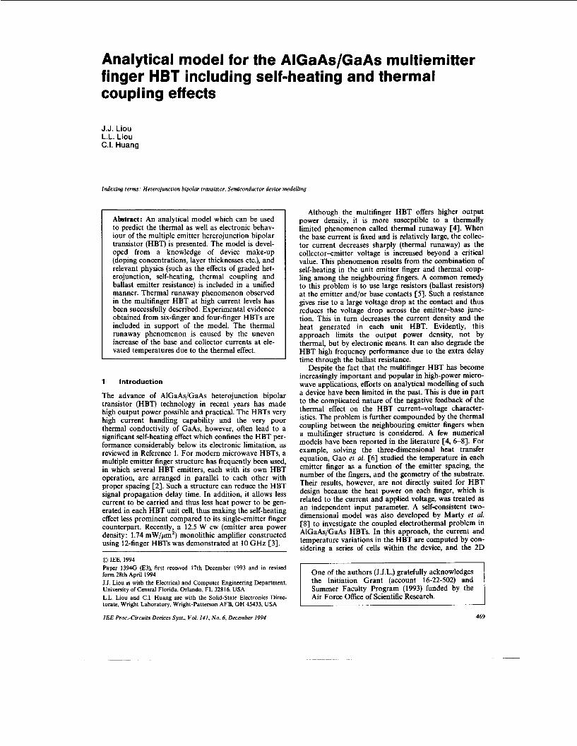
Because the conduction band discontinuity (or spike) in an abrupt HBT can hinder the free-carrier transport from the emitter to base, a graded layer inserted between the emitter and base is often used to improve the free-carrier injection efficiency [ll]. Such a layer, normally having a thickness between 10 and 30 nm, can effectively remove the spike and thus make the thermionic and tunnelling mechanisms at the heterointerface less important. Fig. 1
B
1 graded layer
0 Fig. 1 including a graded layer
Schematic illustration of the one-dimensional HBT structure
shows a simplified AI,,,Ga,,,As/GaAs/GaAs HBT struc- ture in forward-active mode including a graded layer in which the AI composition is graded linearly from 0.3 at x = - W, to 0.0 at x = 0.
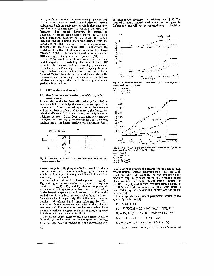
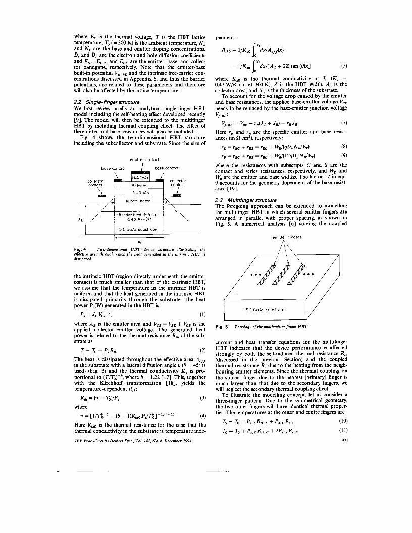
A detailed derivation of the barrier potentials V,,, V,, , B?,. and B,, including the effect of W, is given in Appen- dix 6. Here V,,, V,,, VBsc and V,, denote the potentials in the emitter-side space-charge layer ( -Xl < x < - W,), in the base-side space-charge layer (0 < x < X,), in the graded layer for conduction band and in the graded layer for valence band, respectively. Fig. 2 illustrates the con- duction and valance band edges calculated for W, = 15 nm and three different voltages. Clearly, the spike has been removed. The conduction band edges obtained from the model derived in Appendix 6 and simulation reported in Reference 12 are compared in Fig. 3.
The model for the collector and base current densities (J, and J,) can be developed by incorporating the V,,, V,, , V,, and V,, expressions into the thermionic-field
470
diffusion model developed by Grinberg et d. [13]. The detailed J, and J, model development has been given in Reference 9 and will not be repeated here. It should be
Fig. 3 model andfrom simulation [I23 for W, = 30 nm ~ Model . . . . . . . Simulation W =30nm N: = 2 x IO" cm-' N, = 5 x 10" cm-'
Comparison of the conduction band edges obtained from the
mentioned that important parasitic effects, such as bulk recombination, surface recombination, and the Kirk effect, are taken into account. The first two effects are modelled empirically based on the data available in the literature (e.g., a bulk recombination lifetime of 3 x lo-" s [14] and surface recombination velocity of 2 x lo6 cm/s [l5] are used), and the latter effect is described using the conventional expressions for silicon devices [16].
The temperature-dependent parameters needed in the J, and J, model are [9] :
D, = VT[7200/(1 + 5.5 X l o - 1 7 ~ ~ ) o ' 2 3 3 ] ( ~ O / T ) 2 ~ 3
E,, = 1.87 - 5.4 x 10⁻⁴TZ/(T + 204)
I E E Proc.-Circuits Deuices Syst., Vol. 141, No. 6, December 1994
where VT is the thermal voltage, T is the HBT lattice temperature, To (= 300 K) is the ambient temperature, N E and N E are the base and emitter doping concentrations, D, and D, are the electron and hole diffusion coefficients and EGE , EGB, and E,, are the emitter, base, and collec- tor bandgaps, respectively. Note that the emitter-base built-in potential V,, BE and the intrinsic free-carrier con- centrations discussed in Appendix 6, and thus the barrier potentials, are related to these parameters and therefore will also be affected by the lattice temperature.
2.2 Single-finger structure We first review briefly an analytical single-finger HBT model including the self-heating effect developed recently [9 ] . The model will then be extended to the multifinger HBT by including thermal coupling effect. The effect of the emitter and base resistances will also be included.
Fig. 4 shows the two-dimensional HBT structure including the subcollector and substrate. Since the size of
emitter contact
base contact base contact
collector collector contact contact
\ /
pendent : r X.
= 1/Ks0 F x / [ A , + 2 2 tan (8)x] (5 )
where K,, is the thermal conductivity at To (Fso = 0.47 W/K-cm at 300 K), Z is the HBT width, A, IS the collector area, and X, is the thickness of the substrate.
To account for the voltage drop caused by the emitter and base resistances, the applied base-emitter voltage VBE needs to be replaced by the base.-emitter junction voltage 5. BE :
5. BE = VBE - rdJc + JB) - rB JB (7)
Here rE and rB are the specific emitter and base resist- ances (in cm2), respectively:
rE = *EC + rES = IEC + WE/(qDn NE/vT)
rB = rBc + rBs = ~ B c + W B / ( ~ ~ @ ~ N B / V T )
(8)
(9) where the resistances with subscripts C and S are the contact and series resistances, respectively, and WE and WE are the emitter and base widths. The factor 12 in eqn. 9 accounts for the geometry dependent of the base resist- ance [19] .
2.3 Multifinger structure The foregoing approach can be extended to modelling the multifinger HBT in which several emitter fingers are arranged in parallel with proper spacing, as shown in Fig. 5. A numerical analysis [6] solving the coupled
em1 tter f i ngers I- - 1
AC
Fig. 4 Two-dimensional HET device structure illustrating the effective area through which the heat generated in the intrinsic HET is dissipated
the intrinsic HBT (region directly underneath the emitter contact) is much smaller than that of the extrinsic HBT, we assume that the temperature in the intrinsic HBT is uniform and that the heat generated in the intrinsic HBT is dissipated primarily through the substrate. The heat power P,(W) generated in the HBT is
S I GaAs substrate p , = Jc VCE A€ (1)
where A, is the emitter area and V,, = VBE + VcB is the applied collector-emitter voltage. The generated heat power is related to the thermal resistance Rth of the sub- strate as
T - To = P,Rth (2) The heat is dissipated throughout the effective area A,, in the substrate with a lateral diffusion angle 8 (0 = 45" is used) (Fig. 3) and the thermal conductivity K, is pro- portional to (TITo)-*, where b = 1.22 [17] . This, together with the Kirchhoff transformation [18] , yields the temperature-dependent Rfh :
Rth = (q - (3)
q = [ l / T t - ' - (b - l ) R , h o P s / T ~ ] - ' " b ~ l ~ (4) Here RthO is the thermal resistance for the case that the thermal conductivity in the substrate is temperature inde-
where
I E E Proc.-Circuits Devices Syst., Vol. 141, No. 6, December 1994
Fig. 5 Topology of the multiemitterfinger HET
current and heat transfer equations for the multifinger HBT indicates that the device performance is affected strongly by both the self-induced thermal resistance Rth (discussed in the previous Section) and the coupled thermal resistsance R, due to the heating from the neigh- bouring emitter elements. Since the thermal coupling on the subject finger due to the nearest (primary) finger is much larger than that due to the secondary fingers, we will neglect the secondary thermal coupling effect.
To illustrate the modelling concept, let us consider a three-finger pattern. Due to the symmetrical geometry, the two outer fingers will have identical thermal proper- ties. The temperatures at the outer and centre fingers are
471
where the subscripts S and C denote outer and centre fingers, respectively. The term involving Rlh is the tem- perature rise due to self-heating in the unit HBT and the term involving R, is the temperature rise due to thermal coupling between the subject finger and the nearest (primary) neighbouring finger@). Note that the centre finger is subjected to two thermal couplings whereas the outer fingers are subjected to only one thermal coupling.
The value of R, depends on the geometry of emitter fingers and the process, including the emitter mesa etching and metallisation, and is too complicated to model physically. For typical mesa-etch HBTs, R, has been empirically determined as
R, = 0.25R,,,(10/S)'.5 (12) where S is the emitter-finger spacing (in micrometre). Decreasing S will increase R, and subsequently increase the likelihood of thermal runaway.
The initial value of T can be calculated from the above equations after the initial J,, J,, and P , are calculated under room temperature. This temperature is then used to calculate the initial R, and R, . The correct T , J , and J, for each emitter finger are obtained after several iter- ations. Summing Jc and J , in each finger then yields the total J , and J , for the multifinger HBT.
.. 005rnA
3 Results and discussions
Fig. 6 shows the Gummel plot calculated from the model and obtained from measurement for a six-finger HBT at
100-
10-1-
d 10.2-
: 104-
Z 10-5- s 10-6.
t 10-7-
10-8-
4
C
" 10-4- -
0
0 n
"BE .V
Fig. 8 Base and collector currents calculated form the present model for a six-finger HET at Vc, = 0, 3 and 6 V . Also included are the experi- mental data measwed at Vc, = 0 Six-fmger HET Finger area = 2.5 x 10 pmz rpc = 6.0 x W, = I5 nm
~ Model (V, = 0)
-_ 0.0 Measured Ic(VcB = 0) A A A MeasurcdI,(Vc,=O)
R mz
Model (V, = 3.0 VI Model (V,, = 6.0 V)
_ _ _ -
V,, = 0, 3 and 6 V. The HBT has a typical intrinsic make-up of N E = 5 x lo" C I I - ~ , N, = 8 x lo'* ~ m - ~ , N , = 5 x 10l6 m-', emitter layer thickness of 100 nm, base layer thickness of 100 nm, collector layer thickness of 700nm, a finger area of 2.5 x 10pm2, and a ballast emitter contact resistance of 6 x R cm'. The extrin- sic make-up of the HBT, which is needed to calculate the thermal resistance R,,, is Z = 25 pm, A, = 10 x 25 pm2 and X, = 100 pn. This gives a thermal resistance of
412
about 4OOK/W at room temperature. As shown in the figure, both the collector and base currents (I, and I,) increase as V', is increased. This is due to the fact that the power generated, and therefore the temperature, in the HBT is increased as V,, (V,, = VEE + V,,) increases. But since I, rises more quickly than I,, the current gain will decrease as VcE is increased when the current level is high. This trend is clearly shown in Fig. 7.
1°il
100 1001 IO-^ 10-3 io-l
collector current. A
DC current gain corresponding to the results shown in Fig. 6 Fig. 7 Six-linger HBT
~ v,, = o VcB = 3.0 V
- _ V,. = 6.0 V ~~-~
The model developed can also be used to calculate I, against VcE characteristics for constant I,. The results, together with experimental data, are given in Fig. 8. A
negative slope on the IC& characteristics is observed when the base current is large where the thermal effect becomes prominent. This can be attributed to the uneven increase of I, and I , as Vcs or V,,, is increased (see Fig. 6). The increased I , due to the thermal effect reduces the
IEE Proc.-Circuits Devices Syst., Vol. 141, No. 6, December I994
base-emitter voltage V,, required to maintain that con- stant base current, which subsequently decreases the col- lector current. The values of VB, corresponding to the I / V curves in Fig. 8 are shown in Fig. 9, which indicate that V;, needed to maintain the constant I, is almost constant when the base current is low and is decreased rapidly against V,, when the base current i s high.
1.60r
'. >
I40
0.15mA I35
vCE,v
Fig. 9 I , used in Fig. 8 Six-finger HBT Finger area = 2.5 x 10 p' rrc = 6 x
Note that the experimental data shown in Fig. 8 increases slightly at relatively low I, and large V,, . This is caused by avalanche multiplication in the reverse- biased base-collector junction, an effect not accounted for in the present model. It is interesting to see that the elevated temperature at higher I, seems to offset the ava- lanche effect and subsequently increase the breakdown voltage.
Even with a ballast resistance, thermal runaway can still prevail, but is less obvious and occurs only if V,, is sufficiently large. This is evidenced by the 'minor thermal runaway' at I , = 0.35 mA and V, 2 7 V shown in Fig. 8. The thermal runaway results from the even more asym- metrical increase in the base and collector currents a t higher base current seen in Fig. 6 (at V,, = 1.45 V and V,, = 6 V). If I, is fixed, then the voltage V,, required to maintain that I, will also decrease sharply when V,, is increased beyond a critical value (see Fig. 9), which then decreases sharply the collector current. As will be shown later, the thermal runaway is much more apparent if the HBT does not have a ballast emitter resistance.
We next examine the effect of the emitter contact resistance rEc on the HBT performance. Here we consider a three-finger HBT. Fig. 10 shows the Gummel plot for three different r,, and V,, = 2 V. The same plot for a larger V,, (= 5 V) is given in Fig. 11. Obviously, the increased rEc suppresses both the collector and base cur- rents at high V,,. Of equal importance to note is the behaviour of the collector current at large rEc and when V,, is high. Let us use the results in Figs. 10 and 11 to illustrate this point. Consider first the nonballast ( IEc =
R an') and a fix I, = 1 mA. When V,, = 2 V (or V,, o 3 V), V,, x 1.62V and I, o 0.2 A. As V,, is increased to 5 V (V,, o 6 V), V,, x 1.44 V, and the cor- responding IC is about 0.1 A, which has been decreased to about 50% of its previous value (thermal runaway occurs).
Now let us consider the HBT with a ballast resistance (rEC = 2.5 x R an2) and fix I, at 0.3 mA (the
The required base-emitter voltage V,, to maintain the constant
n m1
I E E Proc.-Circuits Devices Syst., Vol. 141, No. 6 , December 1994
maximum value shown in Fig. IO). At V,, = 3 V, the cor- responding I, is 0.04 A, and at V,, = 6 V, I, is about 0.035 A. Thus the collector current in this case is decreased slightly, but not decreased significantly, as V,, is increased from 2 to 6 V.
lOOr
10-81
Fig. 10 far three different emitter contact resistances at Vc, = 2 V
rz = 5 x 10⁻⁶ncm' Three-finger HBT _ _ - _ r,=2.5 x ~ o - ~ n ~ ~ Finger area = 2.5 x 10 ,nu1
~ r , , = l ~ l O - ~ n c m ~ V,=ZV
Base and collector currents calculatedfiom the present nwdel
_ _
O1
VEE.~
Fig. 11 for three diferent emitter contact resistances at V', = 5 V
Base and collector currents calculatedfrom the present model
~ rEC = 1 x 10⁻⁶nmf _ _ _ _ r , = 5 x l O - 6 n m '
TBC = 2.5 x 10⁻⁵ n c m l v,, = 5 v _ _
The emitter-finger temperatures corresponding to the results in Fig. 11 are shown in Fig. 12. Note that the temperature at the centre finger is higher than that at the outer fingers, which arises from the fact that the centre finger is subjected to two thermal coupling whereas the outer fingers are subjected to only one thermal coupling.
The thermal runaway phenomenon in a multifinger HBT without the ballast emitter resistance discussed above can be clearly illustrated with the I /V character- istics shown in Fig. 13. The device considered has four emitter fingers, a finger area of 2.5 x 20 pm2, and a low emitter contact resistance (rEc x R cm'). The onset of thermal runaway is observed at V,, s 5 V when I, is increased beyond 2.5 mA.
4 Conclusion
Temperature increase due to self-heating and thermal coupling has been known as a major factor limiting the
473
performance of AlGaAs/GaAs multiple emitter HBTs. An analytical model has been developed to describe the DC behaviour of such devices. The effect of the graded heterojunction, a feature used frequently to improve the
5 0 -
40 4 E - c 30-
3 ” 3 3 - 20- 8
550r
-
3501 I Y I
VBE .V
Fig. 12 considered in Fig. IO and Vc, = 5 V Thra-finger HBT v,, = 5 v
~ Tc s
Temperatures at the centre and outerfingers for the
_ _ _ -
i g : 30 rnA \ 2 0 r n A , . - _ . . . . 1 5 r n A . . . . o . . . . . .
device
“CEsV Fig. 13 Collector current against collector-emitter voltage charncter- istics as a function af constant I , for a four-finger HET without ballast emitter resistance Four-iinger HBT Finger area = 2.5 x 20 pn’ rEc = 1 x __ Model 0.0 Measurements
n cm’
HBT emitter injection efficiency, is also accounted for in the model. We found that an elevated temperature in the HBT due to the thermal effect increases the base current more quickly than the collector current. This uneven current increase is the main mechanism contributing to the thermal runaway phenomenon observed in high power HBTs. Our results also suggest that while thermal runaway can occur in all HBTs with sufficiently high current level and applied voltage, incorporating a ballast resistance in the emitter contact can reduce the extent of thermal runaway. The model predictions compare favourably with data measured from a six-finger HBT with a ballast emitter resistance and a four-finger HBT without a ballast emitter resistance.
The model developed describes the thermally limited HBT DC characteristics comprehensively for practical
474
applications, including for use in HBT design and circuit simulation. Avalanche multiplication at very large collector-emitter voltages, however, was not treated and may form a subject of future research.
5 References
1 KIM, M.E., BAYRAKTAROGLU, B., and GUF’TA, A.: ‘HBT devices and applications’, in ALI, F., and GUPTA, A. (Eds.): ‘HEMTs & HBTs: devices, fabrication, and circuits’ (Artech House, Boston, 1991)
2 WANG, N.L., SHENG, N.H., CHANG, M.F., HO, W.J., SULLI- VAN, G.J., SOVERO, E.A., HIGGINS, J.A., and ASBECK, P.M.: ‘Ultrahigh power effkiency operation of common-emitter and common-base HBTs at 10 GHz’, IEEE Trans. Microwave Theory & Tech., 1990,38, pp. 1381-1389
3 KHATIBZADEH, M.A., BAYRAKTAROGLU, B., and KIM, T.: ‘12 W monolithic X-hand HBT power amplifier’. IEEE MlT-S international microwave symposium dig., 1992, pp. 47-50
4 LIOU, L.L., BAYRAKTAROGLU, B., and HUANG, C.1.: Thermal stability analysis of multiple finger microwave AlGaAs/ GaAs heterojunction bipolar transistor’. IEEE international micro- wave symposium tech. dig., 1993
5 GAO, G.B., UNLU, M.S., MORKOC, H., and BLACKBURN, D.L.: ‘Emitter ballasting resistor design for current handling capa- bility of AIGaAslGaAs power heterojunction bipolar transistors’, IEEE Trans. Electron Devices, 1991.38, pp. 185-196
6 GAO, G.B., WANG, M.-Z., GUI, X., and MORKOC, H.: ‘Thermal design studies of high-power heterojunction bipolar transistors’, IEEE Trans. Electron Devices, 1989, ED-36, pp. 854-862
7 WHITEFIELD, D.S., WEI, C.J., and HWANG, J.C.M.: ‘Temperaturedependent large-signal model of heterojunction bipolar transistors’. IEEE GaAs IC Symposium Tech. Dig., 1992, pp. 221-224
8 MARTY, A., CAMPS, T., TASSELLI, I., PULFREY, D.L., and BAILBE, J.P.: ‘A selfconsistent DC-AC two-dimensional electro- thermal model for GaAIAslGaAs microwave wwer HBTs’, IEEE Trans. Electron Devices, 1993.40, pp. 1202
~
9 LIOU, J.J., LIOU, L.L., HUANG, C.I., and BAYRAKTAROGLU, B.: ‘A physics-base heterojunction bipolar transistor including thermal and highcurrent effects’, IEEE Trans. Electron Devices, 1993,40, p. 1570
10 CHEN, S.-C., SU, Y.-K., and LEE, C.-Z.: ‘A study of current trans- port on p-N heterojunctions’, Solid-state Electron., 1982, 35, pp. 1311
1 1 DAS, A., and LUNDSTROM, M.S.: ‘Numerical study of emitter- base junction design for AlGaAs/GaAs heterojunction bipolar tran- sistors’, IEEE Trans. Electron Devices, 1988,35, pp. 863
12 TIWARI, S., and FRANK, D.J.: ‘Analysis of the operation of GaAIAsIGaAs HBTs’, IEEE Trans. Electron Devices, 1989, 36, pp. 2105
13 GRINBERG, A.A., SHUR, M.S., FISCHEQ R.J., and MORKOC, H.: ‘An investigation of the effect of graded layers and tunnelling on the performance of AIGaAsIGaAs heterojunction bipolar tran- sistors’, IEEE Trans. Electron Devices, 1984, ED-31, pp. 1758
14 STRAUSS, U,, HEBERLE, A.P., ZHOU, X.Q., RUHLE, W.W., LAUTERBACH, T., BACHEM, K.H., and HAEGEL, N.M.: ‘Minoritv-carrier lifetime in heavilv doued GaAs: C‘, Jap. J. Appl. . .. . . Phys., 1693, 32, p. 495
15 TIWARI, S., FRANK, D.F., and WRIGHT, S.L.: ‘Surface recombi- nation in GaAlAsIGaAs heterojunction bipolar transistors’, J. Appl. Phvs.. 1988.61. D. 5009
16 KfRK, C.T. Jr.1 ‘A theory of transistor cutoff frequency falloff at high current densities’, IRE Trans. Electron Devices, 1962, ED-9,
17 MAYCOCK, D.P.: ‘Thermal conductivity of silicon, germanium, 111-V compound and 111-V alloys’, Solid-state Electron, 1967, 10, p. 161
18 JOYCE, W.B.: ‘Thermal resistance of heat sink with temperature- dependent conductivity’, Solid-State Electron., 1975,18, pp. 321
19 YUAN, J.S., LIOU, J.J., and EISENSTADT, W.R.: ‘A physics-based current-dependent base-resistance model for advanced bipolar tran- sistors’, IEEE Trans. Electron Devices, 1988, ED-35, p., 1055
20 ADACHI, S.: ‘GaAs, AlAs, and Al,Ga,_,As: matenal parameters for use in research and device application’, J. Appl. Phys., 1985, SS, pp. Rl-R29
21 CHAITERJEE, A., and MARSHAK, A.H.: ‘Theory of abrupt het- erojunctions in equilibrium’, Solid-State Electron., 1981, U, pp. 1 1 11
22 WONG, W.I.: ‘On the band offset of AlGaAsIGaAs and beyond’, Solid-state Electron., 1986.29, pp. 133
PP. 164
IEE Proc.-Circuits Devices Syst., Vol. 141, No. 6, December 1994
6 Appendix
The dielectric permittivity E,(x) in the linearly grade layer is
(13) where E, and are the dielectric permittivities in the emitter and base, respectively, and We is the graded layer thickness (Fig. 1). For the A1o.,Gao,,As/GaAs junction, E, = 12.2 c0 and eg = 13.1 c0 [20]. Thus E, = (0.93
For the graded layer having a position-dependent per-
dZ V / d x 2 = - { ~ / E , ( x ) + ( ~ V / ~ X ) [ ~ E , ( X ) / ~ X ] / E , ( X ) }
= - [(E€ - & E ) / K l X + ELI
+ & E .
mittivity, the one-dimensional Poisson equation is
= - {P/&AX) - (dV/dX)[(E€ - E B ) / & l / E g ( X ) - 1 (14)
where V is the electrostatic potential and p is the space- charge density. Employing the depletion approximation, the electric fields TAX) = - d V / d x in the graded layer can be derived from eqn. 14 as
5,(x) = t,@) + [4N, WJ(0.93 E011
x In [l + 0.93 z0 x/( W, 4 1 for - W, < x < 0 (15)
where N , is the emitter doping concentration. Similarly, the electric fields t z ( x ) and tl(x) on the base and emitter sides of the space-charge region can be derived as
t z ( X ) = (qNg/EgXXZ - X) for 0 d X d x2
C1(x) = (qN,/e,XX, + x ) for - X I d x < -We (16)
(17)
where NE is the base doping concentrations, and X , and X, are the thicknesses on the emitter and base sides of the space-charge region, respectively (see Fig. 1). Since the flux density at x = 0 is continuous, t,(O) needed in eqn. 15 can be readily obtained from eqn. 16 as r,(O) =
Choose x = - X , as the reference point. The corre- sponding electrostatic potentials V ( x ) can be obtained by integrating t ( x ) over their boundaries :
qNE x 2 / E E .
Vi(x) = 0.5 (qNE/E,&X1 + x)'
for - X , < x < -W, (18) Vg(X) = 0.5 ((IN,IE,MXi - Wg)' + ( 4 N d z / % )
x (X + W,) + 0.5 (qNJEg)(XZ - W i ) - ( q N d 6 )
x C0.93 eO/(We~:)](x3 + W:) for -We 6 x < 0 (19)
Using the same approach and noting that the total elec- trostatic potential across the space-charge region is hi, - V,, the electrostatic potential V,(x) on the base side of the junction is given by
b ( X ) = bi, BE - VBE - 0.5 (qNB/EidXz - XI2
for 0 d x d X , (20)
where V,, is the emitter-base junction built-in potential C211, and V,, is the base-emitter applied voltage.
The space-charge region thickness X , can be solved from eqns. 19 and 20 using the condition that the poten- tial is continuous at x = 0 [V,(O) = V,(O)]:
X , = -0.5 A,/Al - 0.5 (A: - 4A1A3)0.5/A, (21)
where
A, = -0.5 qN$&, - 0.5 qN;/(/(E,N,)
A2 = 4NB We/% - q N , W g / h
A , = V,, - V,, + 0.5 q N , W ~ / E , - 0.5 q N , W ~ / & E
+ qN, Wi(0.93 E~/E:)/~
Since the flux density is continuous at x = - W,, the rela- tion between x , and x , can be derived by equating eqns. 15 and 17 at x = - W,.
For the case of We = 0 (abrupt junction), A , = 0, A , = V,,,, - V,, and eqn. 21 reduces to
xz = {~%,BE - %E)EE%NdqNB(%NE + & B N E ) ] } ~ . ~
(22)
which is the conventional space-charge region thickness model for an abrupt heterojunction.
The barrier potentials are readily obtained from eqns. 18-20 :
VEI = 0.5 (qNE/E.dXi - YJz (23)
VBgC = -AEc/q + qNEX2 W,/EB - 0.5 qN, Wi/E,
- (qNJ6M0.93 EO WilEg) (24)
- (qNd6X0.93 eo W ~ / E ; ) (25)
vBZ = 0.5 (qNdEE)X: (26)
Vi,, = AEv/q + d'"Xz W,/&E - 0.5 qNE W i / b
where V,, is the conduction (or valence) bond barrier potential for the region of x = - X I and x = - W,, VEgc is the conduction band barrier potential for the graded layer ( -We < x i 0), V,,, is the valence band barrier potential for the graded layer, and V,, is the conduction (or valence) band barrier potential for the region of x = 0 and x = X , . Note that the conduction and valence band discontinuities AEc and AEv are accounted for in the conduction band and valence barrier potentials V,, and VBeu associated with the graded layer, respectively. Also, BE, = 0.6AEG(AEG = AE,, - AEGE = 0.37 eV the energy bandgap difference) and AEv = BE, - A& = 0.4 AE, [22].
The values of V,,, can be positive or negative depend- ing on the applied voltage and thickness of the graded layer. A positive value indicates the potential has a posi- tive slope, and vice versa if the value is negative. In fact a positive slope implies that the spike has been effectively removed. Note that V'," is always positive and that VBgc and V,,, reduce to -AEc/q and AEv/q, respectively, for an abrupt junction (W, = 0).