Andrew Kahng – June 2003 1 Scope and Goals of Future Design-Through-Mask Integrations Advanced Reticle Symposium June 24, 2003 Andrew B. Kahng, UCSD CSE & ECE Departments email: [email protected]URL: http://vlsicad.ucsd.edu
Transcript
Andrew Kahng – June 2003 1
Scope and Goals of Future Design-Through-Mask Integrations
Advanced Reticle SymposiumJune 24, 2003
Andrew B. Kahng, UCSD CSE & ECE Departmentsemail: [email protected]: http://vlsicad.ucsd.edu
Andrew Kahng – June 2003 2
OutlineOutline• The Problem, Scope and Goals
• Example 1: Performance-Driven Fill
• Example 2: Cost-Driven RET
• Example 3: Intelligent MDP
• Example 4: Analog Rules, Restricted Layout, …
• Conclusions
Andrew Kahng – June 2003 3
The Problem• Steadily increasing design effort, turnaround time,
and project risk
• “Dark Future” (12th Japan DA Show talk, 2000)– Cost and predictability failures – Electronics industry makes workarounds
• platforms programmability software
– Semiconductor industry stalls – No retooling cycle for supplier industries (e.g., EDA)
• Fiddling: Incremental, linear extrapolation of current trajectory– “GDS-3”– Thin post-processing layers (decompaction, RET
insertion, …)
Andrew Kahng – June 2003 5
0%
20%
40%
60%
80%
100%
Intel IBM Synopsys TUE-Magma
Cadence STMicro
Variability/Litho/Mask/Fab Low Power/Leakage
Power Delivery/Integrity Tool/Flow Enhancements/OA
IP Reuse/Abstraction/SysLevel Design DSM Analysis
P&R and Opt Others (Lotto)
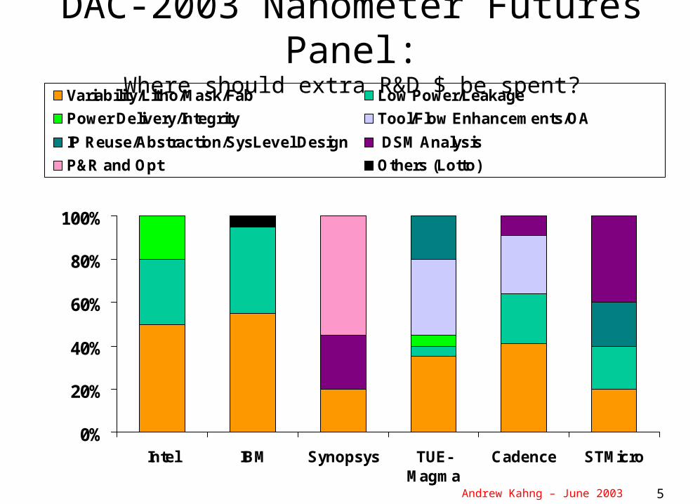
DAC-2003 Nanometer Futures Panel:Where should extra R&D $ be spent?
Andrew Kahng – June 2003 6
Co-Evolutionary Paths• Designer, EDA, and process communities cooperate and co-evolve to maintain the cost (value) trajectory of Moore’s Law
– Must escape Prisoner’s Dilemma– Must be financially viable– At 90nm to 65nm transition, this is a matter of survival for the worldwide semiconductor industry
• Example Focus Areas:– Manufacturability and cost/value optimization– Restricted layout – Intelligent mask data prep– Analog rules– (Layout and design optimizations)– Disclaimer: Not a complete listing
Andrew Kahng – June 2003 7
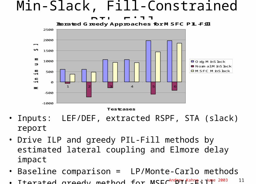
• Bidirectional design-manufacturing data pipe– Fundamental drivers: cost, value
• Pass functional intent to mask flow– Example: RET for predictable circuit performance, function
– RETs should win $$$, reduce performance variation
cost-driven, parametric yield constrained RET
• Pass limits of mask flow up to design– Example: avoid corrections that cannot be manufactured or
Illustration courtesy Cadence Design Systems, Inc.
Andrew Kahng – June 2003 13
OutlineOutline• The Problem, Scope and Goals
• Example 1: Performance-Driven Fill
• Example 2: Cost-Driven RET
• Example 3: Intelligent MDP
• Example 4: Analog Rules, Restricted Layout, …
• Conclusions
Andrew Kahng – June 2003 14
Design for Value*
• Mask cost trend Design for Value (DFV)
Design for Value Problem: Given
• Performance measure f• Value function v(f)
• Selling points fi corresponding to various values of f
• Yield function y(f)
Maximize Total Design Value = i y(fi)*v(fi)[or, Minimize Total Cost]
• Probabilistic optimization regime* See "Design Sensitivities to Variability: Extrapolation and Assessments in Nanometer VLSI", IEEE ASIC/SoC
Conference, September 2002, pp. 411-415.
Andrew Kahng – June 2003 15
Obvious Step: Function-Aware OPC• Annotate features with “required amount” of OPC
– E.g., why correct dummy fill?– Determined by design properties such as setup and hold
timing slacks, parametric yield criticality of devices and features
• Reduce total OPC inserted (e.g., SRAF usage)– Decreased physical verification runtime, data volume– Decreased mask cost resulting from fewer features
• Supported in data formats (OASIS, IBM GL-I)– Design through mask tools need to make, use annotations
Andrew Kahng – June 2003 16
• MinCorr (DAC-2003): Different levels of RET = different levels of CD control
Cost-Driven RET
Type of OPC
Ldrawn (nm)
3 of Ldrawn
Figure Count
Delay (, ) for NAND2X1
Aggressive 130 5% 5X (60.7, 7.03)
Medium 130 6.5% 4X (60.7, 7.47)
No OPC 130 10% 1X (60.7, 8.79)
OPC solutions due to K. Wampler, MaskTools, March 2003
CD studies due to D. Pramanik, Numerical Technologies, December 2002
Andrew Kahng – June 2003 17
• Mapping of area minimization to RET cost optimization• “Yield library” similar to timing libraries (e.g., .lib) Can get an off-the-shelf synthesis tool to perform
OPC “sizing”• Achieves up to 79% reduction in figure complexity
without any loss of parametric yield
MinCorr Results
Gate Sizing MinCorr
Cell Area Cost of correction
Nominal Delay
Delay (+k)
Cycle Time Selling point delay
Die Area Total cost of OPC
Andrew Kahng – June 2003 18
OutlineOutline• The Problem, Scope and Goals
• Example 1: Performance-Driven Fill
• Example 2: Cost-Driven RET
• Example 3: Intelligent MDP
• Example 4: Analog Rules, Restricted Layout, …
• Conclusions
Andrew Kahng – June 2003 19
MDP for Minimum NRE• Mask data prep (MDP)
– Partition layout shapes into multiple gray-scale writing passes
• Idea: mask blanks can be mass-produced and stored to reduce average cost (e.g., $10K), then customized on demand
M. D. Levenson, 2003
Andrew Kahng – June 2003 27
Notes on Regular Layout• 65 nm has high likelihood for layouts to look like regular gratings
– Uniform pitch and width on metal as well as poly layers Predictable layouts even in presence of focus and dose variations
• More manufacturable cell libraries with regular structures • New layout challenges (e.g., preserving regularity in placement)• Caveats
– Non-minimum width poly is less susceptible to variation larger devices (with same W/L) may lead to more robust designs (so, selective “upsizing” may be an alternative to regular layouts)
– 180nm node is a “sweet spot” for cost, analog/mixed-signal integration, etc. more and more technology nodes will tend to coexist
Andrew Kahng – June 2003 28
OutlineOutline• The Problem, Scope and Goals
• Example 1: Performance-Driven Fill
• Example 2: Cost-Driven RET
• Example 3: Intelligent MDP
• Example 4: Analog Rules, Restricted Layout, …
• Conclusions
Andrew Kahng – June 2003 29
Conclusions• Designer, EDA, and mask communities must cooperate and co-evolve to maintain the cost (value) trajectory of Moore’s Law
– Wakeup call: Intel 157nm announcement
• Basic goal: bidirectional design-mask data pipe– Drivers: cost, value– Pass functional intent to mask flow– Pass limits of mask flow up to design
• Example focus areas (not a complete listing!)– Manufacturability and cost/value optimization– Restricted layout – Intelligent mask data prep– Analog rules– (Layout and design optimizations)