532 S. REBELLI, B. R. NISTALA, AN EFFICIENT MRTD MODEL FOR THE ANALYSIS OF CROSSTALK ... An Efficient MRTD Model for the Analysis of Crosstalk in CMOS-Driven Coupled Cu Interconnects Shashank REBELLI , Bheema Rao NISTALA Dept. of E.C.E, National Institute of Technology, Warangal, Telangana, India [email protected], [email protected]Submitted September 15, 2017 / Accepted December 16, 2017 Abstract. This paper presents an efficient wavelet based numerical method for analyzing functional and dynamic crosstalk of CMOS driven coupled copper (Cu) intercon- nects known as Multi-Resolution Time Domain (MRTD), wherein, the CMOS drivers are modeled using n th -power law model. The performance of the proposed MRTD method is evaluated through recursive simulations in HSPICE environ- ment and compared with the conventional Finite Difference Time Domain (FDTD) method at 32-nm technology node for global interconnects of length 1mm, where the computations of the proposed model and conventional FDTD are carried out using MATLAB. For different number of test cases, the proposed MRTD method gives an average error of 0.14% and 1.9 % for peak crosstalk noise and peak noise timing, respectively, with respect to HSPICE results. Also, the dy- namic crosstalk noise on victim line of the proposed MRTD method are in close agreement with those of HSPICE. The re- sults show the dominance of the proposed MRTD method over the conventional FDTD method regarding accuracy. The proposed MRTD method is also extended for three-mutually- coupled interconnect lines for crosstalk analysis, with an av- erage error less than 1 % when compared to that of more than 3 % using the conventional FDTD method. Moreover, for the transient analysis, the MRTD method is more time efficient than HSPICE. Keywords CMOS driver, Cu interconnects, peak crosstalk noise, delay, MRTD, FDTD, HSPICE 1. Introduction With the evolution of deep sub-micron CMOS technol- ogy, the circuits in chips (SOCs) allow Giga-scale integration. In such circuits, the analysis of interconnects have become extremely important to determine the performance of a cir- cuit such as power consumption and time delay. In addition to the delay, with the high operating frequencies, crosstalk is a pitfall in the design of interconnect structures for circuitry. As on-chip circuitry is gradually miniaturized, the adjacent interconnects arebrought into closer proximity. Accordingly, the undesired signal coupling between the interconnects gets elevated [1].So, the precise prediction of peak crosstalk noise and peak noise timing in a driver-interconnect-load (DIL) system has become a critical design view for a long period [1]. For the analysis of the crosstalk noise, most of the earlier models have considered non-linear CMOS driver as a simple linear resistor [2], [3], which leads to a discrepancy in the results. Because, during the transient, MOSFET operates in saturation region about 50 % of its operating time and rest of time in linear (or) cutoff regions [4]. To model a DIL system, several methods have been reported in the recent state of the art works , where differ- ent analytical solutions, the Finite Difference Time Domain (FDTD) method and SPICE solutions are explored [5], [6]. The alpha-power law model used for modeling non-linear CMOS driver and an interconnect line is modeled us- ing the Analytical approach for the analysis of functional crosstalk effects [5] and dynamic crosstalk effects [7]. The models outlined in [5] and [7] is limited to only two cou- pled interconnect lines resulting in dependance on even-odd modes. To analyze the dynamic crosstalk of multiple mu- tually coupled on-chip interconnect lines, Vobulapuram et al. in [8] used FDTD method for modeling of intercon- nect lines where CMOS driver is represented using alpha- power law model. The alpha-power law model becomes imprecise with the technology scaling, as it ignores the fi- nite drain conductance (λ) parameter. Later, in [9], Vobu- lapuram et al. employed n th power law model [10], which includes the finite drain conductance (λ) parameter to repre- sent CMOS driver with FDTD [11] for modeling mutually coupled interconnect lines. The conventional FDTD method is a substantial nu- merical technique for solving partial differential equations and Electromagnetic problems. But the conventional FDTD method is numerically dispersive [12]. The Multiresolution Time-Domain (MRTD) method proposed by Krumpholz et al. in [13] presents significant advantages in numerical dis- persion properties [14]–[17]. In Multiresolution analysis using the Haar scaling function as the basis function, the MRTD algorithm is equally accurate with the conventional FDTD [15]. The Daubechies’ scaling function based MRTD method with three and four vanishing moments shows higher DOI: 10.13164/re.2018.0532 CIRCUITS
Transcript
532 S. REBELLI, B. R. NISTALA, AN EFFICIENT MRTD MODEL FOR THE ANALYSIS OF CROSSTALK . . .
An Efficient MRTD Model for the Analysis of Crosstalk inCMOS-Driven Coupled Cu Interconnects
Shashank REBELLI , Bheema Rao NISTALA
Dept. of E.C.E, National Institute of Technology, Warangal, Telangana, India
Submitted September 15, 2017 / Accepted December 16, 2017
Abstract. This paper presents an efficient wavelet basednumerical method for analyzing functional and dynamiccrosstalk of CMOS driven coupled copper (Cu) intercon-nects known as Multi-Resolution Time Domain (MRTD),wherein, the CMOS drivers are modeled using nth-power lawmodel. The performance of the proposed MRTD method isevaluated through recursive simulations in HSPICE environ-ment and compared with the conventional Finite DifferenceTime Domain (FDTD) method at 32-nm technology node forglobal interconnects of length 1mm, where the computationsof the proposed model and conventional FDTD are carriedout using MATLAB. For different number of test cases, theproposed MRTD method gives an average error of 0.14%and 1.9 % for peak crosstalk noise and peak noise timing,respectively, with respect to HSPICE results. Also, the dy-namic crosstalk noise on victim line of the proposed MRTDmethod are in close agreement with those of HSPICE. The re-sults show the dominance of the proposedMRTDmethod overthe conventional FDTD method regarding accuracy. Theproposed MRTD method is also extended for three-mutually-coupled interconnect lines for crosstalk analysis, with an av-erage error less than 1%when compared to that of more than3% using the conventional FDTD method. Moreover, for thetransient analysis, the MRTD method is more time efficientthan HSPICE.
KeywordsCMOS driver, Cu interconnects, peak crosstalk noise,delay, MRTD, FDTD, HSPICE
1. IntroductionWith the evolution of deep sub-micron CMOS technol-
ogy, the circuits in chips (SOCs) allowGiga-scale integration.In such circuits, the analysis of interconnects have becomeextremely important to determine the performance of a cir-cuit such as power consumption and time delay. In additionto the delay, with the high operating frequencies, crosstalk isa pitfall in the design of interconnect structures for circuitry.As on-chip circuitry is gradually miniaturized, the adjacentinterconnects are brought into closer proximity. Accordingly,
the undesired signal coupling between the interconnects getselevated [1].So, the precise prediction of peak crosstalk noiseand peak noise timing in a driver-interconnect-load (DIL)systemhas become a critical design view for a long period [1].
For the analysis of the crosstalk noise, most of the earliermodels have considered non-linear CMOS driver as a simplelinear resistor [2], [3], which leads to a discrepancy in theresults. Because, during the transient, MOSFET operates insaturation region about 50% of its operating time and rest oftime in linear (or) cutoff regions [4].
To model a DIL system, several methods have beenreported in the recent state of the art works , where differ-ent analytical solutions, the Finite Difference Time Domain(FDTD) method and SPICE solutions are explored [5], [6].The alpha-power law model used for modeling non-linearCMOS driver and an interconnect line is modeled us-ing the Analytical approach for the analysis of functionalcrosstalk effects [5] and dynamic crosstalk effects [7]. Themodels outlined in [5] and [7] is limited to only two cou-pled interconnect lines resulting in dependance on even-oddmodes. To analyze the dynamic crosstalk of multiple mu-tually coupled on-chip interconnect lines, Vobulapuram etal. in [8] used FDTD method for modeling of intercon-nect lines where CMOS driver is represented using alpha-power law model. The alpha-power law model becomesimprecise with the technology scaling, as it ignores the fi-nite drain conductance (λ) parameter. Later, in [9], Vobu-lapuram et al. employed nth power law model [10], whichincludes the finite drain conductance (λ) parameter to repre-sent CMOS driver with FDTD [11] for modeling mutuallycoupled interconnect lines.
The conventional FDTD method is a substantial nu-merical technique for solving partial differential equationsand Electromagnetic problems. But the conventional FDTDmethod is numerically dispersive [12]. The MultiresolutionTime-Domain (MRTD) method proposed by Krumpholz etal. in [13] presents significant advantages in numerical dis-persion properties [14]–[17]. In Multiresolution analysisusing the Haar scaling function as the basis function, theMRTD algorithm is equally accurate with the conventionalFDTD [15]. The Daubechies’ scaling function based MRTDmethod with three and four vanishing moments shows higher
DOI: 10.13164/re.2018.0532 CIRCUITS
RADIOENGINEERING, VOL. 27, NO. 2, JUNE 2018 533
accuracy than conventional FDTD [16]. The MRTD methodusing the Daubechies’ scaling function as the basis functionfor the transient analysis of transmission lines shows a bet-ter dispersion property than the FDTD method [18]. How-ever, the MRTD method has not been used to calculate thecrosstalk noise and delay of CMOS driven coupled on-chipinterconnects in the present state of the art works.
This paper adopted theMRTD [18] method for the anal-ysis of crosstalk noise of VLSI interconnects. To drive theinterconnect lines a non-linear CMOS driver is considered,which is modeled using nth power law model [10].
The rest of the paper is organized as follows: Section 2discusses the formulation of the MRTD method for coupledCu interconnect lines. Section 3 describes the simulationsetup and the validation of the results for two and threecoupled interconnects, followed by conclusion in Sec. 4.
2. Formulation of the MRTD MethodThe proposed MRTD method is developed using
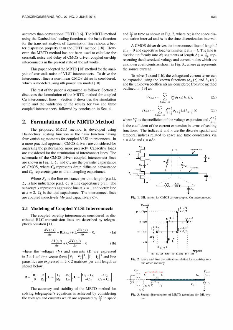
Daubechies’ scaling function as the basis function havingfour vanishing moments for coupled VLSI interconnects. Ina more practical approach, CMOS drivers are considered foranalyzing the performance more precisely. Capacitive loadsare considered for the termination of interconnect lines. Theschematic of the CMOS-driven coupled interconnect linesare shown in Fig. 1. Cd and Cm are the parasitic capacitanceof CMOS, where Cd represents drain diffusion capacitanceand Cm represents gate-to-drain coupling capacitance.
Where Rx is the line resistance per unit length (p.u.l.),Lx is line inductance p.u.l. Cx is line capacitance p.u.l. Thesubscript x represents aggressor line at x = 1 and victim lineat x = 2. CL is the load capacitance. The interconnect linesare coupled inductively MC and capacitively CC.
2.1 Modeling of Coupled VLSI InterconnectsThe coupled on-chip interconnects considered as dis-
tributed RLC transmission lines are described by telegra-pher’s equation [11].
∂V (z, t)∂z
+ RI (z, t) + L∂I (z, t)∂t
= 0, (1a)
∂I (z, t)∂z
+ C∂V (z, t)∂t
= 0 (1b)
where the voltages (V) and currents (I) are expressedin 2 × 1 column vector form
[V1 V2
]T,[I1 I2
]T and lineparasitics are expressed in 2 × 2 matrices per unit length asshown below.
R =[R1 00 R2
], L =
[L1 MCMC L2
], C =
[C1 + CC −CC−CC C2 + CC
].
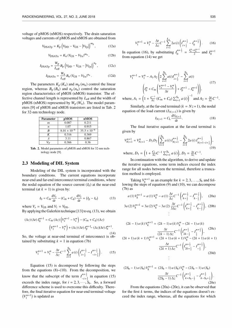
The accuracy and stability of the MRTD method forsolving telegrapher’s equations is achieved by consideringthe voltages and currents which are separated by ∆z2 in space
and ∆t2 in time as shown in Fig. 2, where ∆z is the space dis-cretization interval and ∆t is the time discretization interval.
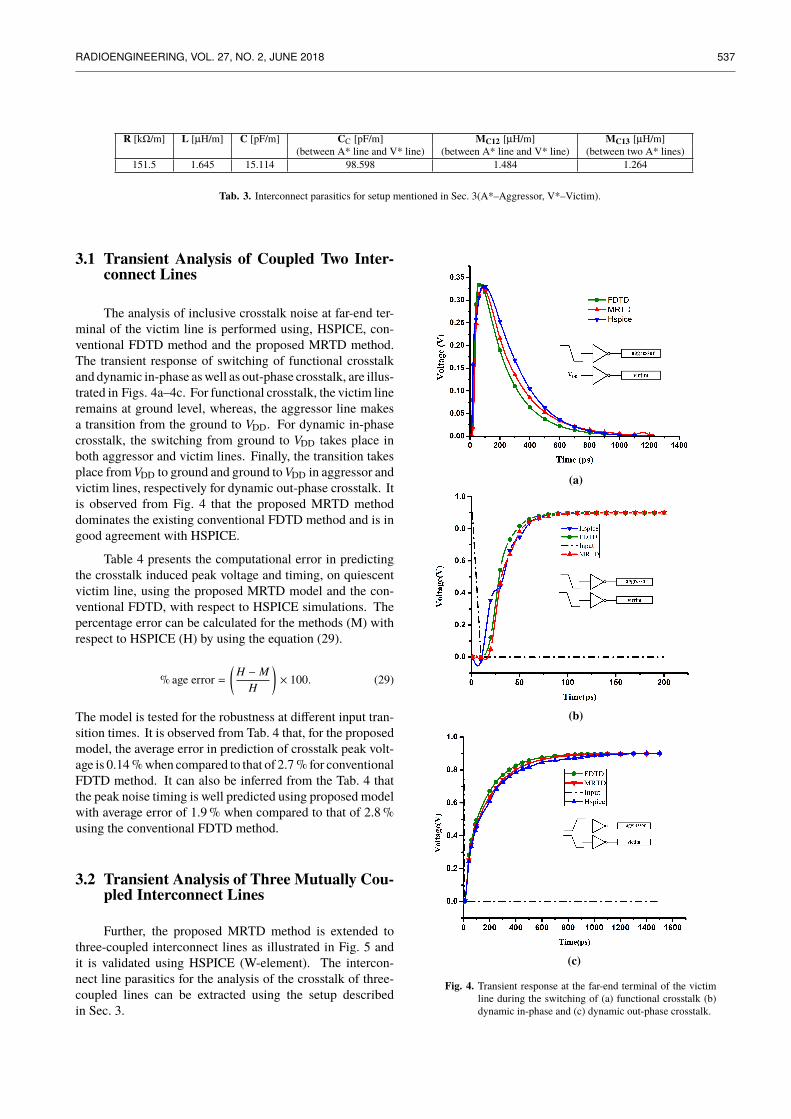
A CMOS driver drives the interconnect line of length lat z = 0 and capacitive load terminates it at z = l. The line isdivided uniformly into Nz segments of length ∆z = l
Nz , rep-resenting the discretized voltage and current nodes which areunknown coefficients as shown in Fig. 3., where I0 representsthe source current.
To solve (1a) and (1b), the voltage and current terms canbe expanded using the known functions (φk (z) and hn (t) )and the unknown coefficients are considered from themethodoutlined in [13] as:
V (z, t) =+∞∑
k,n=−∞
Vnk φk (z) hn (t) , (2a)
I (z, t) =+∞∑
k,n=−∞
In+ 1
2k+ 1
2φk+ 1
2(z) hn+ 1
2(t) (2b)
whereVnkis the coefficient of the voltage expansion and I
n+ 12
k+ 12
is the coefficient of the current expansion in terms of scalingfunctions. The indices k and n are the discrete spatial andtemporal indices related to space and time coordinates viaz = k∆z and t = n∆t.
Fig. 1. DIL system for CMOS driven coupled Cu interconnects.
Fig. 2. Space and time discretization relation for acquiring sec-ond order accuracy.
Fig. 3. Spatial discretization of MRTD technique for DIL sys-tem.
534 S. REBELLI, B. R. NISTALA, AN EFFICIENT MRTD MODEL FOR THE ANALYSIS OF CROSSTALK . . .
The function hn (t) and φk (z) is defined as:
hn (t) = h( t∆t− n
), (3)
φk (z) = φ(
z∆z− k
)(4)
where h (t) represents a Haar scaling function and φ (z) rep-resents a Daubechies’ scaling function.
To derive the MRTDmethod for equation (1a) and (1b),the following integrals [19] are considered:
〈hn (t) , hn′ (t)〉 = δn,n′∆t, (5a)
〈φk (z) , φk′ (z)〉 = δk,k′∆z, (5b)⟨hn (t) ,
∂hn′+ 12(t)
∂t
⟩= δn,n′ − δn,n′+1, (6a)⟨
φk (z) ,∂φk′+ 1
2(z)
∂z
⟩=
Sb−1∑i=−Sb
a (i) δk+i,k′ (6b)
where δk,k′ and δn,n′ represents the Kronecker symbol. Inequation (6b) Sb denotes the effective support size of thebasis functions. The coefficients a(i) are called connectioncoefficients. By considering Daubechies’ scaling functionhaving four vanishing moments (D4) as the basis functions,Tab. 1 shows a(i) for 1 ≤ i ≤ Sb, whereas a(i) for i > Sbare zero and for i < 1 it can be obtained by the symmetryrelation a(−1 − i) = −a(i).
Applying the Galerkin technique [13] to equations (1a)and (1b) using the test functions φk+ 1
2hn (t) and φkhn+ 1
2(t),
the following iterative equations for the currents and voltagesare obtained:
In+ 3
2k+ 1
2= B1I
n+ 12
k+ 12− B2
∆t∆z
L−1Sb∑i=1
a (i)(Vnk+i − Vn
k−i+1
), (7a)
Vn+1k = Vn
k −∆t∆z
C−1Sb∑i=1
a (i)(In+ 1
2k+i− 1
2− I
n+ 12
k−i+ 12
), (7b)
where B1 =(LR +
∆t2
)−1 (LR −
∆t2
), B2 =
(1 + ∆t2 RL−1
)−1.
In the iterative equations (7a) and (7b), not only thenear-end boundary voltage Vn+1
1 and far-end boundary volt-age Vn+1
Nz+1 are derived but also the iterative equations of thevoltages and currents near the boundaries also need to beupdated. Near the boundaries the voltages are representedby Vn+1
i and Vn+1Nz+1−ifor i = 2, 3, · · ·, Sb and the currents by
In+ 1
2i+ 1
2and I
n+ 12
Nz+1−i+ 12
i = 1, 2, 3, · · ·, Sb − 1. All these voltagesand currents have some terms that exceed the index range initerative equations (7a) and (7b).
i Connection coeff. a(i) for D41 1.31103407732 −0.15601001103 0.04199574604 −0.00865432365 0.00083086956 0.00001089997 0.0000000041
Tab. 1. Connection coefficients a(i) of Daubechies’ scalingfunctions (D4) [16].
For updating the iterative equations of voltages and cur-rents, equation (7a) and (7b) need to be decomposed usingthe relation in [20], which satisfies the coefficients a(i) givenby
Sb∑i=1(2i − 1)a(i) = 1. (8)
Substituting (8) into (7b), we get
Sb∑i=1(2i − 1) a (i)Vn+1
k =
Sb∑i=1(2i − 1) a (i)Vn
k −
Sb∑i=1
∆t(2i − 1)
∆zC−1[(2i − 1)a(i)
(In+ 1
2k+i− 1
2− I
n+ 12
k−i+ 12
)].
(9)
Considering the corresponding terms with i, we can decom-pose (7b) as:(2i − 1) a (i)Vn+1
k = (2i − 1) a (i)Vnk − (2i − 1) a (i)
∆t(2i − 1)∆z
C−1(In+ 1
2k+i− 1
2− I
n+ 12
k−i+ 12
),
for i = 1, 2, 3, . . . , Sb.
(10)
Equation (10) is further modified by applying theboundary conditions as illustrated in Sec. 2.2 and Sec. 2.3respectively.
2.2 Modeling of CMOS DriverThe CMOS drivers are modeled using nth power law
model that considers the effect of finite drain conductance pa-rameter (λ) along with velocity saturation. During transientsimulation the operation of the pMOS and nMOS transistorsare in either linear, saturation (or) cutoff regions [4].
The pMOS and nMOS current equations using nth
power law model are
Ip =
IDSATp(1 + λp (VDD − VDS)
) (2 − VDD−VDS
VDSATp
) (VDD−VDSVDSATp
)VDS > VDD − VDSATp
(linear)IDSATp
(1 + λp (VDD − VDS)
)VDS ≤ VDD − VDSATp
(saturation)0 VGS ≥ VDD −
VTp(cutoff)
(11a)
In =
IDSATn (1+λnVDS)(2− VDS
VDSATn
) (VDS
VDSATn
)VDS < VDSATn(linear)
IDSATn (1 + λnVDS) VDS ≥ VDSATn(saturation)
0 VGS ≤ VTn(cutoff)
(11b)
where IDSATp (IDSATn), λp (λn), VDSATp (VDSATn), andVTp (VTn) are the drain saturation current, finite drain conduc-tance parameter, drain saturation voltage and the threshold
RADIOENGINEERING, VOL. 27, NO. 2, JUNE 2018 535
voltage of pMOS (nMOS) respectively. The drain saturationvoltages and currents of pMOS and nMOS are obtained from
VDSATp = Kp(VDD − VGS −
VTp)mp, (12a)
VDSATn = Kn (VGS − VTn)mn , (12b)
IDSATp =WpLeff
Bp(VDD − VGS −
VTp)np , (12c)
IDSATn =WnLeff
Bn (VGS − VTn)nn . (12d)
The parameters Kp (Kn) and mp (mn) control the linearregion, whereas Bp (Bn) and np (nn) control the saturationregion characteristics of pMOS (nMOS) transistor. The ef-fective channel length is represented by Leff and the width ofpMOS (nMOS) represented by Wp (Wn). The model param-eters [9] of pMOS and nMOS transistors are listed in Tab. 2for 32-nm technology node.
Tab. 2. Model parameters of pMOS and nMOS for 32-nm tech-nology node [9].
2.3 Modeling of DIL SystemModeling of the DIL system is incorporated with the
boundary conditions. The current equations incorporatenear-end and far-end interconnect terminal conditions, wherethe nodal equation of the source current (I0) at the near-endterminal (at k = 1) is given by:
I0 = CmdVsdt− (Cm + Cd)
dV1dt+
(Ip − In
)(13)
where Vs = VGS and V1 = VDS.Byapplying theGalerkin technique [13] to eq. (13), we obtain
(∆z) (∆t) In+10 = Cm (∆z)
(Vn+1s − Vn
s
)− (Cm + Cd) (∆z)(
Vn+11 − Vn
1
)+ (∆z) (∆t) In+1
p − (∆z)(∆t) In+1n .
(14)So, the voltage at near-end terminal of interconnect is ob-tained by substituting k = 1 in equation (7b)
Vn+11 = Vn
1 −∆t∆z
C−1Sb∑i=1
a (i)(In+ 1
2i+ 1
2− I
n+ 12
−i+ 32
). (15)
Equation (15) is decomposed by following the stepsfrom the equations (8)–(10). From the decomposition, weknow that the subscript of the term I
n+ 12
−i+ 32in equation (15)
exceeds the index range, for i = 2, 3, · · ·, Sb. So, a forwarddifference scheme is used to overcome this difficulty. There-fore, the final iterative equation for near-end terminal voltage(Vn+1
1)is updated as
Vn+11 = Vn
1 −∆t∆z
C−1Ls∑i=1
2a (i)(In+ 1
2i+ 1
2− I
n+ 12
0
). (16)
In equation (16), by substituting In+ 1
20 =
In0 +In+10
2 and In+10
from equation (14) we get
Vn+11 = Vn
1 − A1 A2
(2
Sb∑i=1
a(i)In+ 1
2i+ 1
2−
Sb∑i=1
a(i)(In0 + Cm
(Vn+1s − Vn
s
∆t
)+ In+1
p − In+1n
)),
(17)
where, A1 =(1 + C−1
∆z (Cm + Cd)∑Sb
i=1 a (i))−1
and A2 =∆t∆zC−1.
Similarly, at the far-end terminal (k = Nz+1), the nodalequation of the load current (INz+1) is given by
INz+1 = CLdVNz+1
dt. (18)
The final iterative equation at the far-end terminal isgiven by
Vn+1Nz+1 = Vn
Nz+1 − D1D2
(Sb∑i=1
a (i) In+ 1
2Nz+1 −
Sb∑i=1
2a (i) In+ 1
2Nz+1−i+ 1
2
),
(19)where, D1 =
(1 + CL
∆z C−1 ∑Sbi=1 a (i)
), D2 =
∆t∆zC−1.
In continuation with the algorithm, to derive and updatethe iterative equations, some term indices exceed the indexrange for all nodes between the terminal, therefore a trunca-tion method is employed.
Taking Vn+1k
as an example for k = 2, 3, . . . , Sb and fol-lowing the steps of equation (9) and (10), we can decompose(7b) as
a (1)Vn+1k = a (1)Vn
k − a (1)∆t∆z
C−1(In+ 1
2k+ 1
2− I
n+ 12
k− 12
), (20a)
3a (2)Vn+1k = 3a (2)Vn
k − 3a (2)∆t
3∆zC−1
(In+ 1
2k+ 3
2− I
n+ 12
k− 32
), (20b)
...
(2k − 1) a (k)Vn+1k = (2k − 1) a (k)Vn
k − (2k − 1) a (k)∆t
(2k − 1)∆zC−1
(In+ 1
22k− 1
2− I
n+ 12
12
),
(20c)
(2k + 1) a (k + 1)Vn+1k = (2k + 1) a (k + 1)Vn
k − (2k + 1) a (k + 1)∆t
(2k + 1)∆zC−1
(In+ 1
22k+ 1
2− I
n+ 12
− 12
),
(20d)...
(2Sb − 1) a (Sb)Vn+1k = (2Sb − 1) a (Sb)Vn
k − (2Sb − 1) a (Sb)∆t
(2Sb − 1)∆zC−1
(In+ 1
2k+Sb−
12− I
n+ 12
k−Sb+12
).
(20e)From the equations (20a)–(20e), it can be observed that
for the first k terms, the indices of the equations doesn’t ex-ceed the index range, whereas, all the equations for which
536 S. REBELLI, B. R. NISTALA, AN EFFICIENT MRTD MODEL FOR THE ANALYSIS OF CROSSTALK . . .
the index terms exceed the index range appear in the restSb − k terms. As Sb − k terms go out-of-bounds, these equa-tions are unavailable for forming iterative equations inMRTDmethod. To avoid this problem, a truncation is made in theequations where the index range is exceeding.
By summing up the first k terms in equa-tions (20a)–(20e), we can obtain the modified iterative equa-tions for k = 2, 3, · · ·, Sb
Vn+1k = Vn
k −
(k∑i=1(2i − 1) a (i)
)−1
D2
(k∑i=1
a (i)(In+ 1
2k+i− 1
2− I
n+ 12
k−i+ 12
)).
(21)
Using the same steps illustrated in equa-tions (20a)−(20e), a modified iterative equations of voltagesat interior points as shown in equation (22) and voltages nearthe load as shown in equation (23).
For k = Sb + 1, Sb + 2, · · ·,Nz − Sb,Nz − Sb + 1,
Vn+1k = Vn
k − D2
(Sb∑i=1
a (i)(In+ 1
2k+i− 1
2− I
n+ 12
k−i+ 12
)), (22)
for k = Nz − Sb + 2,Nz − Sb + 3, · · ·,Nz,
Vn+1k = Vn
k −
(Nz−k+1∑i=1
(2i − 1) a (i)
)−1
D2
(Nz−k+1∑i=1
a (i)(In+ 1
2k+i− 1
2− I
n+ 12
k−i+ 12
)).
(23)
The iterative equations of current can be updated byfollowing the same steps of voltage iterative equations witha slight difference. As shown in Fig. 3, it is observed thatthe current nodes appear at the half-integer points, whichmeans that all the currents are located at the interior pointsof terminals. So, the currents near the terminals need to bemodified.
For the iterative equations of current near the terminals,we need to decompose (7a) by using the steps from volt-age iterative equations. The final modified current iterativeequations are obtained as
for k = 1, near the source
In+ 3
21+ 1
2= B1I
n+ 12
1+ 12− B2
∆t∆z
L−1(Sb∑i=1
a (i)(Vn+1i+1 − Vn+1
1
)), (24)
for k = 2, 3, · · ·, SbIn+ 3
2k+ 1
2= B1I
n+ 12
k+ 12− B2
(k∑i=1(2i − 1) a (i)
)−1
∆t∆z
L−1(
k∑i=1
a (i)(Vn+1k+i − Vn+1
k−i+1
)),
(25)
for k = Sb + 1, Sb + 2, · · ·,Nz − Sb,Nz − Sb + 1 , iterativeequations at interior points are
In+ 3
2k+ 1
2= B1I
n+ 12
k+ 12− B2
∆t∆z
L−1(Sb∑i=1
a (i)(Vn+1k+i − Vn+1
k−i+1
)), (26)
for k = Nz − Sb + 2,Nz − Sb + 3, · · ·,Nz, iterative equationsnear the load are
In+ 3
2k+ 1
2= B1I
n+ 12
k+ 12− B2
(Nz−k+1∑i=1
(2i − 1) a (i)
)−1
∆t∆z
L−1(Nz−k+1∑
i=1a (i)
(Vn+1k+i − Vn+1
k−i+1
)).
(27)
A bootstrapping approach is used for evaluating the updatedvoltage and current iterative equations. Foremost, the volt-age iterative equations are solved at fixed time using equa-tions (17), (19), (21)–(23) in terms of past values of voltagesand currents. Thereafter, the iterative equations of currentsare solved from equations (24)–(27) in terms of voltages eval-uated initially and past values of currents. So, to get the stableoutput for theMRTD iterative equations, the courant stabilitycondition [18], [20] is considered as
∆t ≤q∆zϑ
(28)
which states that the propagation time must be greater thanthe time step, over each cell. where q is a Courant numbergiven by q = 1∑Ls
i=1 |a(i) |= ϑ∆t∆z and ϑ is the phase velocity of
propagation on the line.
3. Simulation Setup and Validation ofResultsThe proposed MRTD method is validated in HSPICE
using W-element method and compared with the conven-tional FDTD method. The coupled interconnect lines aredriven using symmetric CMOS drivers. To maintain thesymmetry in operation of CMOS inverter, the aspect ratio ofWp toWn is chosen to be 2 : 1, with thewidth of pMOS (Wp) ischosen to be 3.2 µm. A ramp signal falling from 0.9V(VDD)to 0V with a transition time of 10 ps, is given as an inputto the CMOS driver of aggressor line. The technology usedis 32-nm with thickness and width of the interconnect lineas 0.66 µm and 0.22 µm respectively, with an aspect ratio of3:1 [9]. The height from the ground plane is considered to beequal to the thickness of the interconnect line and the spacingbetween the two interconnect lines is assumed to be equal toits width. The global level interconnect length, load capac-itance and inter-layer metal-insulator dielectric constant ofthe line are 1 mm, 2 fF and 2.2 respectively. The line para-sitics extracted using the setup mentioned above are shownin Tab. 3.
The corresponding mode velocities, for givenline parasitics, are calculated as odd mode ve-locity ϑo = 1.71 × 10⁸ m/s and even mode velocityϑe = 1.45 × 10⁸ m/s. To obtain high accuracy, the value ofspace discretization (∆z) is computed to be less than 0.46mm,by considering break frequency of 32 GHz and even modevelocity. The time discretization (∆t) value is calculated tobe 1.869 ps by using the value of (∆z) and odd mode velocityfor the Courant number q = 0.7.
RADIOENGINEERING, VOL. 27, NO. 2, JUNE 2018 537
R [kΩ/m] L [µH/m] C [pF/m] CC [pF/m] MC12 [µH/m] MC13 [µH/m](between A* line and V* line) (between A* line and V* line) (between two A* lines)
151.5 1.645 15.114 98.598 1.484 1.264
Tab. 3. Interconnect parasitics for setup mentioned in Sec. 3(A*–Aggressor, V*–Victim).
3.1 Transient Analysis of Coupled Two Inter-connect Lines
The analysis of inclusive crosstalk noise at far-end ter-minal of the victim line is performed using, HSPICE, con-ventional FDTD method and the proposed MRTD method.The transient response of switching of functional crosstalkand dynamic in-phase aswell as out-phase crosstalk, are illus-trated in Figs. 4a–4c. For functional crosstalk, the victim lineremains at ground level, whereas, the aggressor line makesa transition from the ground to VDD. For dynamic in-phasecrosstalk, the switching from ground to VDD takes place inboth aggressor and victim lines. Finally, the transition takesplace fromVDD to ground and ground toVDD in aggressor andvictim lines, respectively for dynamic out-phase crosstalk. Itis observed from Fig. 4 that the proposed MRTD methoddominates the existing conventional FDTD method and is ingood agreement with HSPICE.
Table 4 presents the computational error in predictingthe crosstalk induced peak voltage and timing, on quiescentvictim line, using the proposed MRTD model and the con-ventional FDTD, with respect to HSPICE simulations. Thepercentage error can be calculated for the methods (M) withrespect to HSPICE (H) by using the equation (29).
% age error =(
H − MH
)× 100. (29)
The model is tested for the robustness at different input tran-sition times. It is observed from Tab. 4 that, for the proposedmodel, the average error in prediction of crosstalk peak volt-age is 0.14%when compared to that of 2.7% for conventionalFDTD method. It can also be inferred from the Tab. 4 thatthe peak noise timing is well predicted using proposed modelwith average error of 1.9% when compared to that of 2.8%using the conventional FDTD method.
3.2 Transient Analysis of Three Mutually Cou-pled Interconnect Lines
Further, the proposed MRTD method is extended tothree-coupled interconnect lines as illustrated in Fig. 5 andit is validated using HSPICE (W-element). The intercon-nect line parasitics for the analysis of the crosstalk of three-coupled lines can be extracted using the setup describedin Sec. 3.
(a)
(b)
(c)
Fig. 4. Transient response at the far-end terminal of the victimline during the switching of (a) functional crosstalk (b)dynamic in-phase and (c) dynamic out-phase crosstalk.
538 S. REBELLI, B. R. NISTALA, AN EFFICIENT MRTD MODEL FOR THE ANALYSIS OF CROSSTALK . . .
Tab. 4. Computational error involved for peak crosstalk noise and peak noise timing on victim line (conv.*–conventional).
The coupling capacitance between the two aggressor lines canbe neglected safely as the spacing between them is large [21].
R =R1 0 00 R2 00 0 R3
, L =
L1 MC12 MC13MC12 L2 MC12MC13 MC12 L3
,
C =C1 + CC −CC 0−CC C1 + 2CC −CC
0 −CC C1 + CC
.The comparison of the transient response of crosstalk
switching on victim line for three-coupled interconnect linesbetween the proposed MRTD method, HSPICE and the con-ventional FDTD method for two different test cases are il-lustrated in Fig. 6. It is observed that the proposed MRTDmethod is in good agreement with the HSPICE simulationresults. From Figs. 6a and 6b it is also observed that a peak isresulted in the response using the conventional FDTDmethoddue to its numerical dispersion properties. However, theproposed MRTD method with its great advantages in nu-merical dispersion properties [14]–[17] dominates over theconventional FDTDmethodwith respect to accuracy. Table 5presents the computational error involved in predicting thecrosstalk induced 50% delay on victim line due to aggressorlines using the proposed MRTD method and the conven-tional FDTDmethod with respect to HSPICE. Table 5 showsthat the proposed model has an average error less than 1%,whereas, the conventional FDTDmethod has an average errormore than 3%.
The elapsed CPU time for the proposed MRTDmethod, the conventional FDTD method and theHSPICE (W-Element method) is determined using theIntel Core i7 - 3770 CPU (3.40GHz). Table 6 shows the cor-responding elapsed CPU times of eachmethod. It is observedthat both MRTD and conventional FDTD methods are fasterthan HSPICE with respect to simulation time, conventionalFDTD being slightly faster than the proposedMRTD, since itrequires slightly more number of iterations than conventionalFDTD. Therefore, there is a trade-off between accuracy andsimulation time.
Fig. 5. Schematic of CMOS driven three-coupled interconnectlines.
(a)
(b)Fig. 6. Crosstalk induced 50% Delay analysis on victim line
due to aggressor lines (a) test case-1, (b) test case-2 forthree-coupled interconnect lines.
RADIOENGINEERING, VOL. 27, NO. 2, JUNE 2018 539
Input Switching Mode 50% Delay [ps] on Victim line%age error
Test Aggressor Victim Aggressor HSPICE Proposed conv.* Proposed conv.*Cases line1 line line2 HSPICE Model FDTD Model FDTD1 VDD to 0 VDD to 0 VDD to 0 35 34.43 33.89 1.91 3.452 VDD to 0 VDD to 0 VDD 66.088 66.88 64.2 -1.198 2.86
Tab. 5. Computational error involved for 50% Delay on victim line of three-coupled interconnects (conv.*–conventional).
Tab. 6. Comparison of elapsed CPU time of the methodsfor two and three mutually coupled interconnects(conv.*–conventional).
4. ConclusionAn accurate model to analyze the crosstalk effects in
coupled VLSI interconnects is proposed in this paper. TheCMOS driver analyzed using the nth power law model andcoupled distributive RLC interconnects are modeled usingthe MRTD method. For different number of test cases, theproposed method shows an average error of 0.14% and 1.9%with respect to the peak crosstalk noise and the peak noisetiming, respectively, compared to HSPICE results. For three-mutually-coupled interconnect lines, the average error for theproposed model is less than 1% whereas the average errorfor the conventional FDTD method is more than 3%. It isobserved that the proposed MRTD method is in good agree-ment with HSPICE simulations and dominates the conven-tional FDTD method. Besides, the proposed MRTD methodis more time efficient than HSPICE, although the elapsedCPU time of the proposed MRTD method is higher than theconventional FDTD method. Further, the proposed methodis highly useful for precise estimation of crosstalk in thenext-generation VLSI interconnects.
References
[1] RABAEY, J. M., CHANDRAKASAN, A., NIKOLIC, B. Digital In-tegrated Circuits, A Design Perspective. 2nd ed., Englewood Cliffs(US): Prentice-Hall, 2003. ISBN: 0130909963
[2] AGARWAL,K., SYLVESTER,D., BLAAUW,D.Modeling and anal-ysis of crosstalk noise in coupled RLC interconnects. IEEE Transac-tions on Computer-Aided Design of Integrated Circuits and Systems,2006, vol. 25, no. 5, p. 892–901.DOI: 10.1109/TCAD.2005.855961
[3] CUI, J. P., ZHAO, W. S., YIN, W. Y., et al. Signal transmission anal-ysis of multilayer graphene nano-ribbon (MLGNR) interconnects.IEEE Transactions on Electromagnetic Compatibility , 2012, vol. 54,no. 1, p. 126–132. DOI: 10.1109/TEMC.2011.2172947
[4] KANG, S.-M., LEBLEBICI, Y. CMOS Digital Integrated Circuits:Analysis and Design . 3rd ed., New York (US): McGraw-Hill, 2003.ISBN: 0-07-246053-9
[5] KAUSHIK, B. K., SARKAR, S. Crosstalk analysis for a CMOS-gate-driven coupled interconnects. IEEE Transactions on Computer-Aided Design of Integrated Circuits and Systems, 2008, vol. 27, no. 6,p. 1150–1154. DOI: 10.1109/TCAD.2008.923259
[6] LI, X. C., MAO, J. F., SWAMINATHAN, M. Transient analy-sis of CMOS-gate-driven RLGC interconnects based on FDTD.IEEE Transactions on Computer-Aided Design of IntegratedCircuits and Systems, 2011, vol. 30, no. 4, p. 574–583.DOI: 10.1109/TCAD.2010.2095650
[7] KAUSHIK, B. K., SARKAR, S., AGARWAL, R. P., et al.An analytical approach to dynamic crosstalk in coupled intercon-nects. Microelectronics Journal, 2010, vol. 41, no. 2, p. 85–92.DOI: 10.1016/j.mejo.2009.12.011
[8] VOBULAPURAM, R. K., KAUSHIK, B. K., AMALENDU, P.An accurate model for dynamic crosstalk analysis of CMOSgate driven on-chip interconnects using FDTD method. Mi-croelectronics Journal, 2014, vol. 45, no. 4, p. 441–448.DOI: 10.1016/j.mejo.2014.02.004
[9] VOBULAPURAM, R. K., KAUSHIK, B. K., AMALENDU, P.An accurate FDTD model for crosstalk analysis of CMOS gatedriven coupled RLC interconnects. IEEE Transactions on Elec-tromagnetic Compatibility, 2014, vol. 56, no. 5, p. 1185–1193.DOI: 10.1109/TEMC.2014.2305801
[10] SAKURAI, T., NEWTON, A. R. A simple MOSFET model for cir-cuit analysis. IEEE Transactions on Electron Devices, 1991, vol. 38,no. 4, p. 887–894. DOI: 10.1109/16.75219
[11] PAUL, C. R. Incorporation of terminal constraints in the FDTDanalysis of transmission lines. IEEE Transactions on Elec-tromagnetic Compatibility, 1994, vol. 36, no. 2, p. 85–91.DOI: 10.1109/15.293284
[12] IBRAHIM, M., MICHEL, M.N. Computational Electromagnetics—Retrospective and Outlook. Singapore: Springer Singapore, 2015.(A hybrid MRTD–FDTD technique for efficient field computation.)ISBN: 978-981-287-095-7
[13] KRUMPHOLZ, M., KATEHI, L. P. B. MRTD: new time-domainschemes based on multiresolution analysis. IEEE Transactions onMicrowave Theory and Techniques, 1996, vol. 44, no. 4, p. 555–571.DOI: 10.1109/22.491023
[14] TENTZERIS, E. M., ROBERTSON, R. L., HARVEY, J. F., et al.Stability and dispersion analysis of Battle-Lemarie-based MRTDschemes. IEEE Transactions on Microwave Theory and Techniques,1999, vol. 47, no. 7, p. 1004–1013. DOI: 10.1109/22.775432
[15] GRIVET-TALOCIA, S. On the accuracy of Haar-based multireso-lution time-domain schemes. IEEE Microwave and Guided WaveLetters, 2000, vol. 10, no. 10, p. 397–399. DOI: 10.1109/75.877224
[16] FUJII, M., HOEFER, W. J. R. Dispersion of time domain waveletGalerkin method based on Daubechies’ compactly supported scal-ing functions with three and four vanishing moments. IEEE Mi-crowave and Guided Wave Letters, 2000, vol. 10, no. 4, p. 125–127.DOI: 10.1109/75.846920
[17] ALIGHANBARI, A., SARRIS, C. D. Dispersion properties and ap-plications of the Coifman scaling function based S-MRTD. IEEETransactions on Antennas and Propagation, 2006, vol. 54, no. 8,p. 2316–2325. DOI: 10.1109/TAP.2006.879194
540 S. REBELLI, B. R. NISTALA, AN EFFICIENT MRTD MODEL FOR THE ANALYSIS OF CROSSTALK . . .
[18] TONG, Z., SUN, L., LI, Y., et al. Multiresolution time-domainscheme for terminal response of two-conductor transmission lines.Mathematical Problems in Engineering, 2016, p. 15. ArticleID: 8045749. DOI: 10.1155/2016/8045749
[19] PAN, G. W. Wavelets in Electromagnetics and Device Modeling.Hoboken (US): John Wiley & Sons, 2003. ISBN: 0-471-41901-X
[20] DOGARU, T., CARIN, L. Multiresolution time-domain algorithmusing CDF biorthogonal wavelets. IEEE Transactions on Mi-crowave Theory and Techniques, 2001, vol. 49, no. 5, p. 902–912.DOI: 10.1109/22.920147
[21] DAVIS, J. A., MEINDL, J. D. Compact distributed RLC interconnectmodels-Part II: Coupled line transient expressions and peak crosstalkinmultilevel networks. IEEETransactions onElectronDevices, 2000,vol. 47, no. 11, p. 2078–2087. DOI: 10.1109/16.877169
About the Authors . . .
Shashank REBELLI is currently a Ph.D student in the de-partment of E.C.E at NIT, Warangal India. His researchinterest includes on-chip interconnect modeling and Devicemodeling.
Bheema Rao NISTALA received his Ph.D degree in E.C.Efrom IIT, Bombay, India in 2008. He is currently work-ing as an associate professor in the department of E.C.E atNIT, Warangal India. His research interest includes on-chipinterconnect modeling, on-chip passive components, devicemodeling.