32
Another way to implement a folding ADC J. Van Valburg and R. van de Plassche, An 8-b 650 MHz Folding ADC, IEEE JSSC, vol 27, #12, pp. 1662-6, Dec 1992
| Date post: | 01-May-2018 |
| Category: |
Documents |
| Upload: | trinhthuan |
| View: | 214 times |
| Download: | 1 times |

Another way to implement a folding ADC
J. Van Valburg and R. van de Plassche, An 8-b 650 MHz Folding ADC, IEEE JSSC, vol 27, #12, pp. 1662-6, Dec 1992
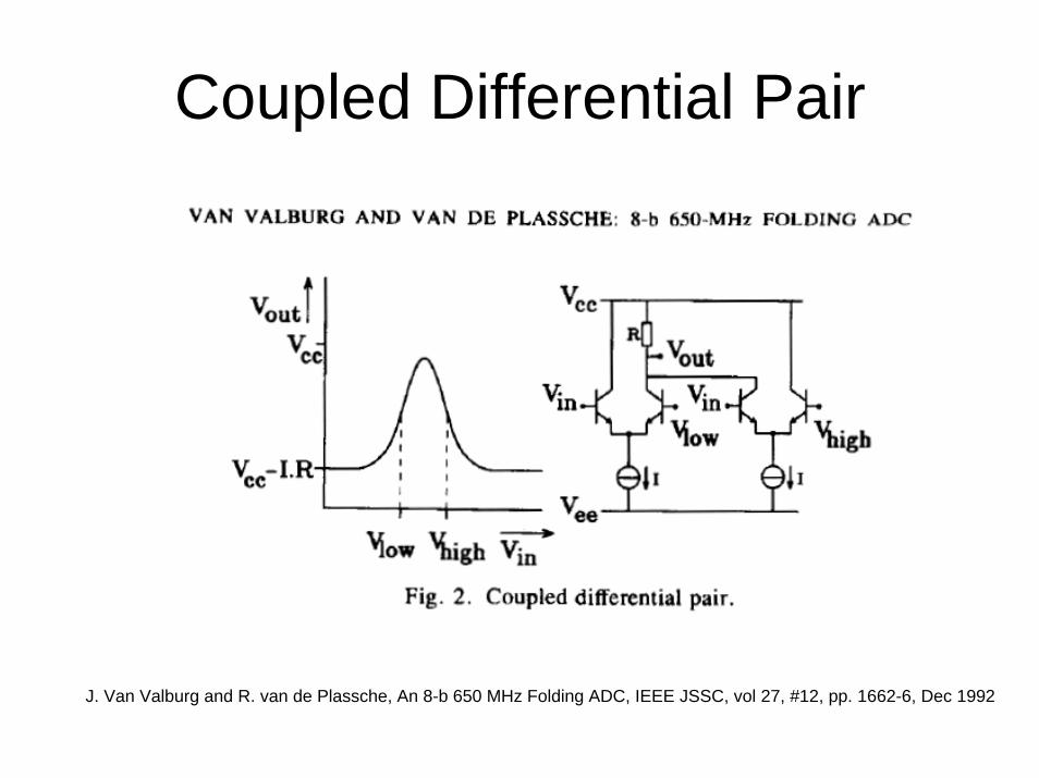
Coupled Differential Pair
J. Van Valburg and R. van de Plassche, An 8-b 650 MHz Folding ADC, IEEE JSSC, vol 27, #12, pp. 1662-6, Dec 1992
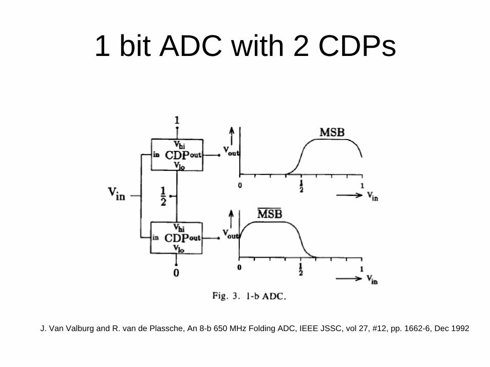
1 bit ADC with 2 CDPs
J. Van Valburg and R. van de Plassche, An 8-b 650 MHz Folding ADC, IEEE JSSC, vol 27, #12, pp. 1662-6, Dec 1992

2-b ADC with 4 CDPs
Folding rate = 44x fIN
J. Van Valburg and R. van de Plassche, An 8-b 650 MHz Folding ADC, IEEE JSSC, vol 27, #12, pp. 1662-6, Dec 1992
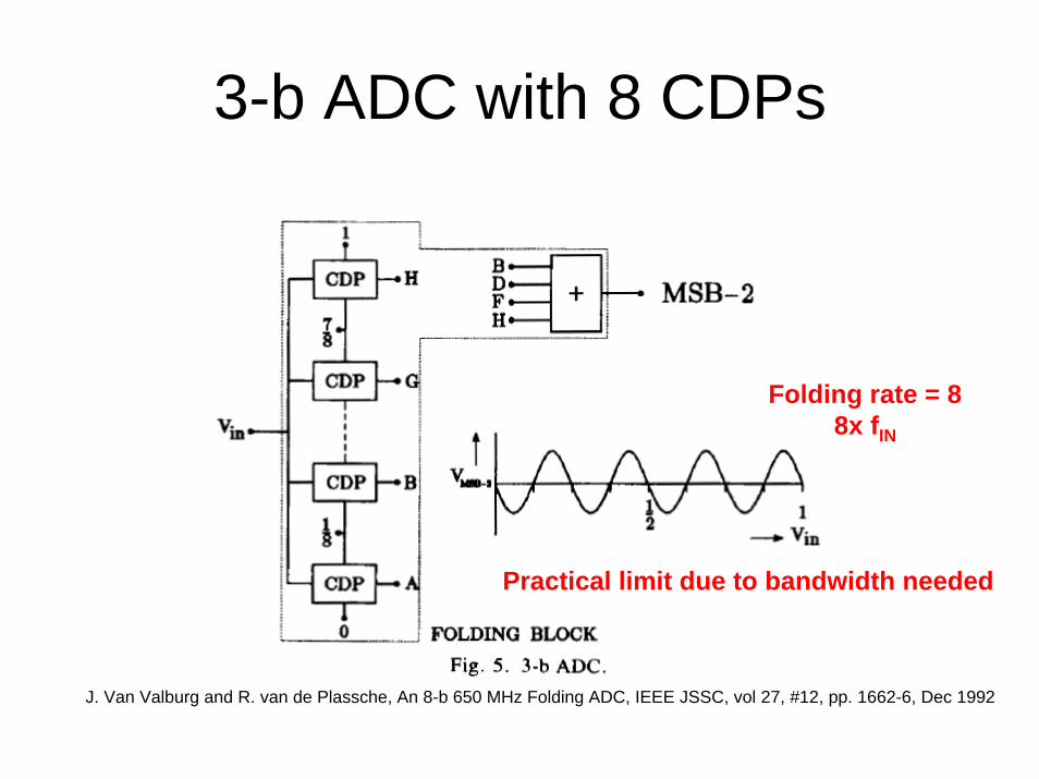
3-b ADC with 8 CDPs
J. Van Valburg and R. van de Plassche, An 8-b 650 MHz Folding ADC, IEEE JSSC, vol 27, #12, pp. 1662-6, Dec 1992
Folding rate = 88x fIN
Practical limit due to bandwidth needed

I-Q folding; offset by ½ LSBResolution can be increased by 1 bit using parallelismwithout increasing folding rate. 4 folding blocks neededto get to 5 bits by folding alone.
You could build all 8 bits this way, but the complexity would be as greatAs a flash converter. So, use interpolation to get the last 3 bits.
J. Van Valburg and R. van de Plassche, An 8-b 650 MHz Folding ADC, IEEE JSSC, vol 27, #12, pp. 1662-6, Dec 1992
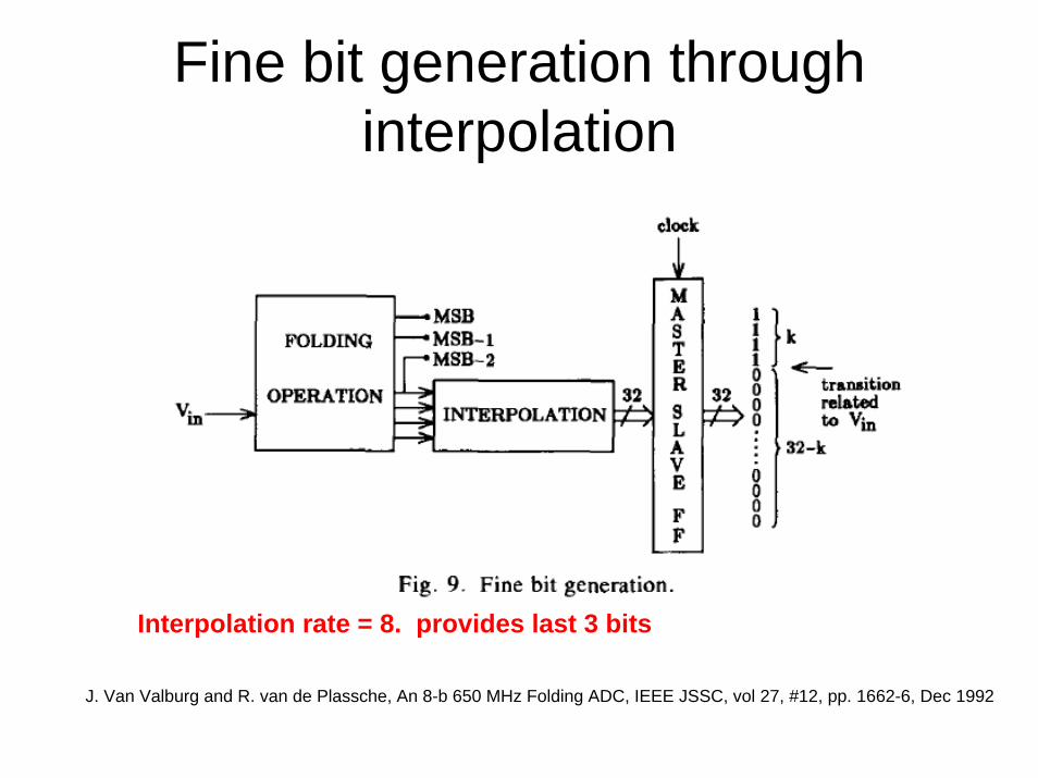
Fine bit generation through interpolation
Interpolation rate = 8. provides last 3 bits
J. Van Valburg and R. van de Plassche, An 8-b 650 MHz Folding ADC, IEEE JSSC, vol 27, #12, pp. 1662-6, Dec 1992

Resistive interpolator
Interpolation rate = 8. provides last 3 bits
J. Van Valburg and R. van de Plassche, An 8-b 650 MHz Folding ADC, IEEE JSSC, vol 27, #12, pp. 1662-6, Dec 1992

Now, the MSFF comparators are all referenced to zero diff input. They are sensing zero crossings
Total number of comparators is reduced (from flash) by folding rate: 256/8=32
J. Van Valburg and R. van de Plassche, An 8-b 650 MHz Folding ADC, IEEE JSSC, vol 27, #12, pp. 1662-6, Dec 1992
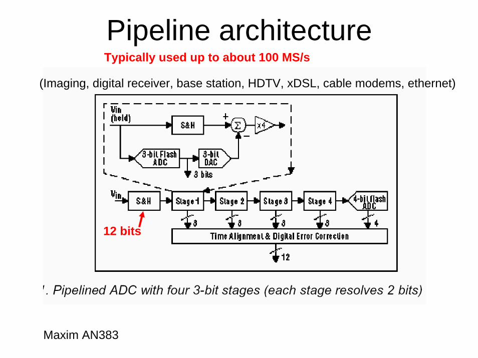
Pipeline architectureTypically used up to about 100 MS/s
(Imaging, digital receiver, base station, HDTV, xDSL, cable modems, ethernet)
12 bits
Maxim AN383

Pipeline example
• Increased sampling rate in exchange for latency• First 4 stages: S/H; 3 bit flash; DAC; residue
multiplied by 4x; 4 bit accuracy.• 2 bits output per stage. Digital error correction
uses 3rd bit to allow extra range in next stage. This can correct for offset errors.
• Final stage must have >4 bit accuracy.• Shift registers needed for digital time alignment

14 bits; 105 MS/s
Analog Devices AD6645 6/2003
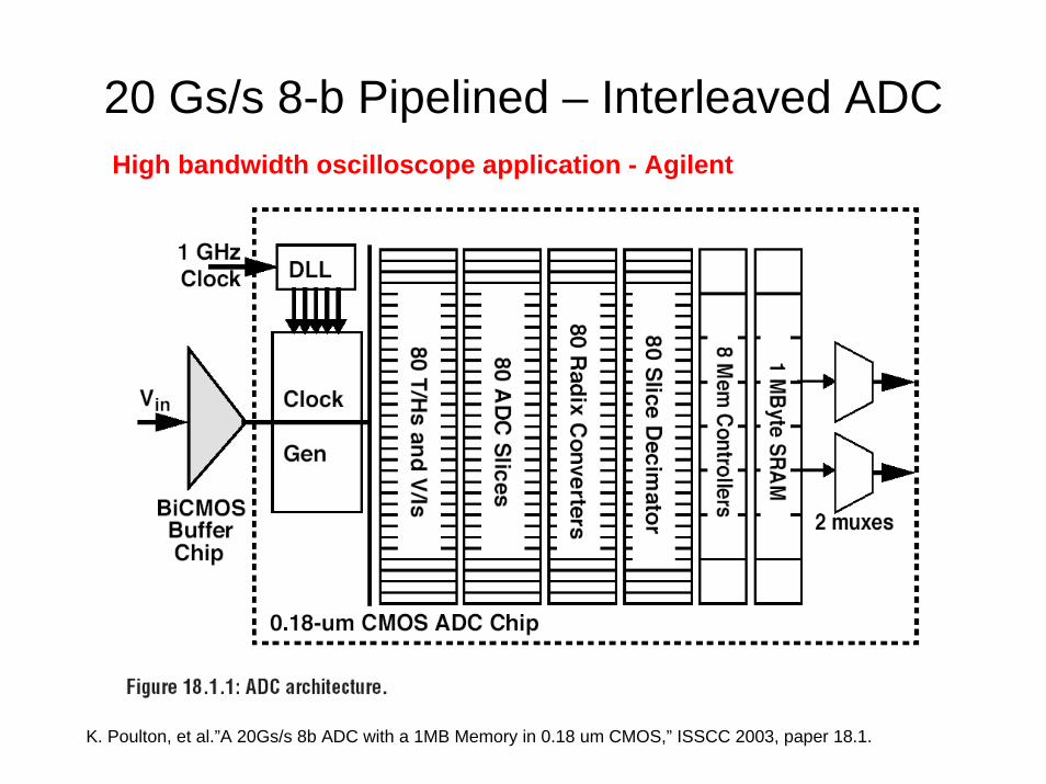
20 Gs/s 8-b Pipelined – Interleaved ADCHigh bandwidth oscilloscope application - Agilent
K. Poulton, et al.”A 20Gs/s 8b ADC with a 1MB Memory in 0.18 um CMOS,” ISSCC 2003, paper 18.1.

Design details
• BiCMOS buffer chip used to drive the 4pF input capacitance of the ADC
• ADC is organized in 80 slices – parallelism used to increase throughput– Each block works at 250 MS/s– T/H, V-I converter, current-mode pipelined 1-bit ADC– Residue is amplified by 1.6X– Radix 1.6 to binary conversion– Data capture in 1MB on-chip SRAM

L-C-L t-lineAdjustable gm to control damping
K. Poulton, et al.”A 20Gs/s 8b ADC with a 1MB Memory in 0.18 um CMOS,” ISSCC 2003, paper 18.1.
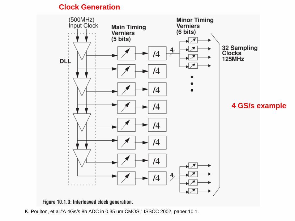
Clock Generation
4 GS/s example
K. Poulton, et al.”A 4Gs/s 8b ADC in 0.35 um CMOS,” ISSCC 2002, paper 10.1.
Clock generation
• The 20 GS/s ADC requires 80 250 MHz clocks, each offset by 50 ps with error < 1ps
• 1 GHz clock; 5 DLL stages => 5 diff clocks• Interpolate to get 20 clocks• Divide by 4 to get 80 clocks• Each has digital time adjustment

Track-Hold slice
Differential transconductor
K. Poulton, et al.”A 4Gs/s 8b ADC in 0.35 um CMOS,” ISSCC 2002, paper 10.1.

Cgs provides hold functionWidth scaling provides gain
ThresholdDetection
Bit outresidue
12 stages of radix 1.6 produces 12 bits; convert to 8 bits binary
K. Poulton, et al.”A 20Gs/s 8b ADC with a 1MB Memory in 0.18 um CMOS,” ISSCC 2003, paper 18.1.
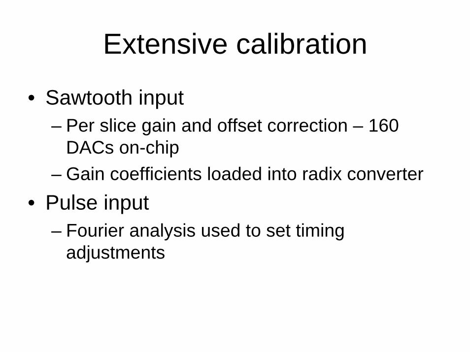
Extensive calibration
• Sawtooth input– Per slice gain and offset correction – 160
DACs on-chip– Gain coefficients loaded into radix converter
• Pulse input– Fourier analysis used to set timing
adjustments

K. Poulton, et al.”A 20Gs/s 8b ADC with a 1MB Memory in 0.18 um CMOS,” ISSCC 2003, paper 18.1.

K. Poulton, et al.”A 20Gs/s 8b ADC with a 1MB Memory in 0.18 um CMOS,” ISSCC 2003, paper 18.1.
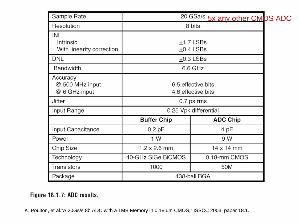
5x any other CMOS ADC
K. Poulton, et al.”A 20Gs/s 8b ADC with a 1MB Memory in 0.18 um CMOS,” ISSCC 2003, paper 18.1.
Analog Devices 4/2005


Analog Devices 11/2004
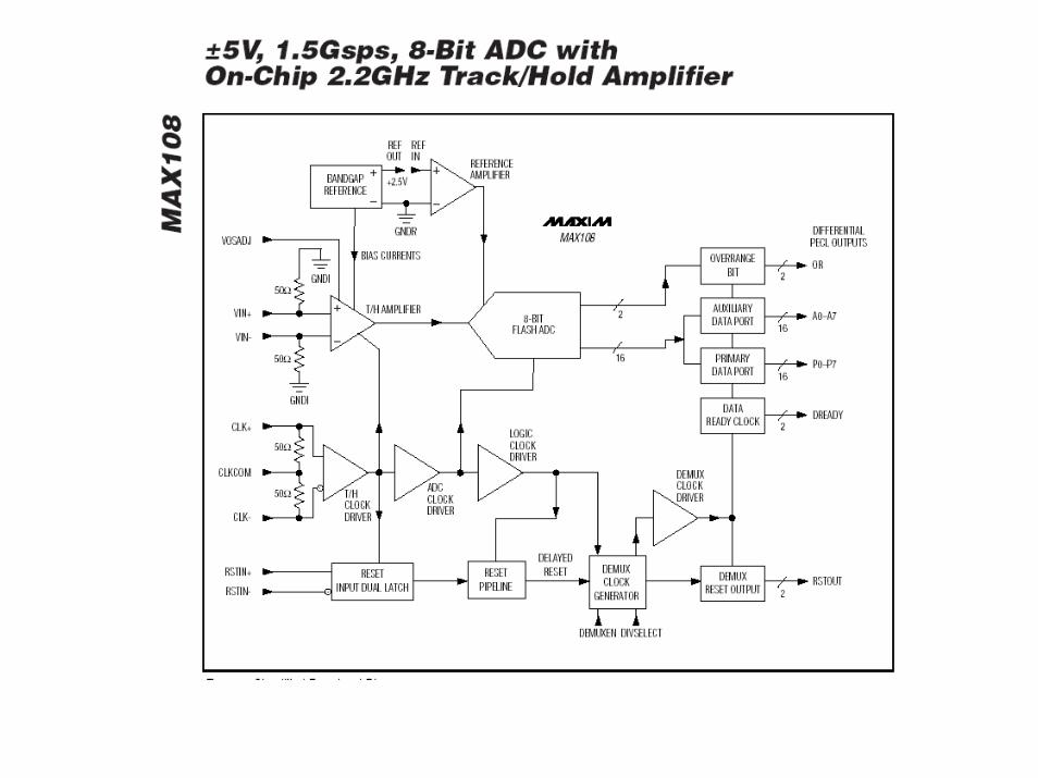

Maxim Integrated Products MAX108

Maxim Integrated Products MAX108

Successive Approximation ADC (SAR ADC)Up to 5 MS/s
8 to 18 bitsLow power
Binary search algorithmStart at midscale: MSB = 1Works down to LSB onebit per cycle
Is VIN < VDAC orVIN > VDAC ?
Maxim AN387

Maxim AN387


