58
Appendix RF Manual 6 th edition May 2005 Semiconductors

Appendix RF Manual 6th edition
May 2005
S e m i c o n d u c t o r s

date of release: May 2005document order number : 9397 750 15125
Contents
1. RF Application-Basics . . . . . . . . . . . . . . . . . . . . . . . . . . . . . . . . . . . . . . . . . . . . . . . . . . . . . . . . . . 51.1 Frequency spectrum . . . . . . . . . . . . . . . . . . . . . . . . . . . . . . . . . . . . . . . . . . . . . . . . . . . . . . . . . . . . . . . 51.2 Function of an antenna . . . . . . . . . . . . . . . . . . . . . . . . . . . . . . . . . . . . . . . . . . . . . . . . . . . . . . . . . . . . . 61.3 Transistor Semiconductor Process . . . . . . . . . . . . . . . . . . . . . . . . . . . . . . . . . . . . . . . . . . . . . . . . . . . . 8
1.3.1 General-Purpose Small-Signal bipolar . . . . . . . . . . . . . . . . . . . . . . . . . . . . . . . . . . . . . . . . . . . . . . . . . 8
1.3.2 Double Polysilicon . . . . . . . . . . . . . . . . . . . . . . . . . . . . . . . . . . . . . . . . . . . . . . . . . . . . . . . . . . . . . . . . 9
2. RF Design-Basics . . . . . . . . . . . . . . . . . . . . . . . . . . . . . . . . . . . . . . . . . . . . . . . . . . . . . . . . . . . . . 102.1 Fundamentals . . . . . . . . . . . . . . . . . . . . . . . . . . . . . . . . . . . . . . . . . . . . . . . . . . . . . . . . . . . . . . . . . . . 10
2.1.1 RF waves . . . . . . . . . . . . . . . . . . . . . . . . . . . . . . . . . . . . . . . . . . . . . . . . . . . . . . . . . . . . . . . . . . . . . . 10
2.1.2 The reflection coefficient . . . . . . . . . . . . . . . . . . . . . . . . . . . . . . . . . . . . . . . . . . . . . . . . . . . . . . . . . . 12
2.1.3 Differences between ideal and practical passive devices . . . . . . . . . . . . . . . . . . . . . . . . . . . . . . . . . 16
2.1.4 The Smith Chart . . . . . . . . . . . . . . . . . . . . . . . . . . . . . . . . . . . . . . . . . . . . . . . . . . . . . . . . . . . . . . . . 17
2.2 Small Signal RF amplifier parameters . . . . . . . . . . . . . . . . . . . . . . . . . . . . . . . . . . . . . . . . . . . . . . . . . . 222.2.1 Transistor parameters DC to microwave . . . . . . . . . . . . . . . . . . . . . . . . . . . . . . . . . . . . . . . . . . . . . 22
2.2.2 Definition of the s-parameters . . . . . . . . . . . . . . . . . . . . . . . . . . . . . . . . . . . . . . . . . . . . . . . . . . . . . 23
2.2.2.1 2-Port network definition . . . . . . . . . . . . . . . . . . . . . . . . . . . . . . . . . . . . . . . . . . . . . . . . . 24
2.2.2.2 3-Port network definition . . . . . . . . . . . . . . . . . . . . . . . . . . . . . . . . . . . . . . . . . . . . . . . . . 25
2.3 RF Amplifier design Fundamentals . . . . . . . . . . . . . . . . . . . . . . . . . . . . . . . . . . . . . . . . . . . . . . . . . . . . 262.3.1 DC bias point adjustment at MMICs . . . . . . . . . . . . . . . . . . . . . . . . . . . . . . . . . . . . . . . . . . . . . . . . . 26
2.3.2 DC bias point adjustment at Transistors . . . . . . . . . . . . . . . . . . . . . . . . . . . . . . . . . . . . . . . . . . . . . . 26
2.3.3 Gain Definition . . . . . . . . . . . . . . . . . . . . . . . . . . . . . . . . . . . . . . . . . . . . . . . . . . . . . . . . . . . . . . . . . . 27
2.3.4 Amplifier stability . . . . . . . . . . . . . . . . . . . . . . . . . . . . . . . . . . . . . . . . . . . . . . . . . . . . . . . . . . . . . . . . 28
3. Introduction into noise . . . . . . . . . . . . . . . . . . . . . . . . . . . . . . . . . . . . . . . . . . . . . . . . . . . . . . . . 303.1 Definition of the equivalent noise source and noise temperature . . . . . . . . . . . . . . . . . . . . . . . . . . . . .303.2 Determine the equivalent noise sources . . . . . . . . . . . . . . . . . . . . . . . . . . . . . . . . . . . . . . . . . . . . . . .313.3 Noisy two-port device: the noise figure and SNR . . . . . . . . . . . . . . . . . . . . . . . . . . . . . . . . . . . . . . . . .323.4 Noise Figure terminated by the amplifiers own semiconductor noise . . . . . . . . . . . . . . . . . . . . . . . . . .333.5 Noise Figure versus noise temperature . . . . . . . . . . . . . . . . . . . . . . . . . . . . . . . . . . . . . . . . . . . . . . . .343.6 Noise Figure versus noise temperature . . . . . . . . . . . . . . . . . . . . . . . . . . . . . . . . . . . . . . . . . . . . . . . .343.7 Noise temperature of a lossy device (attenuator, cable etc.) . . . . . . . . . . . . . . . . . . . . . . . . . . . . . . . .353.8 Noise temperature of a resistor . . . . . . . . . . . . . . . . . . . . . . . . . . . . . . . . . . . . . . . . . . . . . . . . . . . . .353.9 Cascading noisy blocks . . . . . . . . . . . . . . . . . . . . . . . . . . . . . . . . . . . . . . . . . . . . . . . . . . . . . . . . . . . .363.10 Example: a main satellite receiver system design . . . . . . . . . . . . . . . . . . . . . . . . . . . . . . . . . . . . . . . . .363.11 Antenna noise . . . . . . . . . . . . . . . . . . . . . . . . . . . . . . . . . . . . . . . . . . . . . . . . . . . . . . . . . . . . . . . . . . .383.12 Example:A radar system . . . . . . . . . . . . . . . . . . . . . . . . . . . . . . . . . . . . . . . . . . . . . . . . . . . . . . . . . . .393.13 Input and output related noise temperature . . . . . . . . . . . . . . . . . . . . . . . . . . . . . . . . . . . . . . . . . . . .403.14 Amplifier sourced by a noisy generator . . . . . . . . . . . . . . . . . . . . . . . . . . . . . . . . . . . . . . . . . . . . . . . .403.15 Noise Figure, noise temperature & sensitivity of a receiver . . . . . . . . . . . . . . . . . . . . . . . . . . . . . . . . .413.16 Noise sources in semiconductor devices . . . . . . . . . . . . . . . . . . . . . . . . . . . . . . . . . . . . . . . . . . . . . . .413.17 Frequency range of the noise contributions . . . . . . . . . . . . . . . . . . . . . . . . . . . . . . . . . . . . . . . . . . . . .443.18 Sideband noise in oscillators and mixers . . . . . . . . . . . . . . . . . . . . . . . . . . . . . . . . . . . . . . . . . . . . . . .443.19 Equivalent input related noise source . . . . . . . . . . . . . . . . . . . . . . . . . . . . . . . . . . . . . . . . . . . . . . . . . .46
4. Performance of cascaded RF Blocks . . . . . . . . . . . . . . . . . . . . . . . . . . . . . . . . . . . . . . . . . . . . . . 484.1 Receiver dynamic range . . . . . . . . . . . . . . . . . . . . . . . . . . . . . . . . . . . . . . . . . . . . . . . . . . . . . . . . . . . .484.2 Cascaded gain . . . . . . . . . . . . . . . . . . . . . . . . . . . . . . . . . . . . . . . . . . . . . . . . . . . . . . . . . . . . . . . . . . .484.3 Cascaded noise . . . . . . . . . . . . . . . . . . . . . . . . . . . . . . . . . . . . . . . . . . . . . . . . . . . . . . . . . . . . . . . . . .484.4 Cascaded intermodulation . . . . . . . . . . . . . . . . . . . . . . . . . . . . . . . . . . . . . . . . . . . . . . . . . . . . . . . . . .494.5 Cascaded compression . . . . . . . . . . . . . . . . . . . . . . . . . . . . . . . . . . . . . . . . . . . . . . . . . . . . . . . . . . . .514.6 Transmission distance . . . . . . . . . . . . . . . . . . . . . . . . . . . . . . . . . . . . . . . . . . . . . . . . . . . . . . . . . . . . .524.7 Example: transmission distance limited by frequency and receiver quality . . . . . . . . . . . . . . . . . . . . . . .534.8 Filters in the receiver rail . . . . . . . . . . . . . . . . . . . . . . . . . . . . . . . . . . . . . . . . . . . . . . . . . . . . . . . . . .544.9 Relationships and conversion of distortion parameters . . . . . . . . . . . . . . . . . . . . . . . . . . . . . . . . . . . .54
5. Introduction GPS Front-End . . . . . . . . . . . . . . . . . . . . . . . . . . . . . . . . . . . . . . . . . . . . . . . . . . . 55

A survey of the frequency bands and related wavelengths:
Band Frequency Definition Wavelength - p CCIR Bandacc. DIN40015
VLF 3kHz to 30kHz Very Low Frequency 100km to 10km 4LF 30kHz to 300kHz Low Frequency 10km to 1km 5MF 300kHz to 1650kHz Medium Frequency 1km to 100m 6
1605KHz to 4000KHz Boundary WaveHF 3MHz to 30MHz High Frequency 100m to 10m 7
VHF 30MHz to 300MHz Very High Frequency 10m to 1m 8UHF 300MHz to 3GHz Ultra High Frequency 1m to 10cm 9SHF 3GHz to 30GHz Super High Frequency 10cm to 1cm 10EHF 30GHz to 300GHz Extremely High Frequency 1cm to 1mm 11… 300GHz to 3THz … 1mm-100µm 12
Philips RF Manual 6th Edition – Appendix 5
1. RF Application-Basics
1.1 Frequency spectrum
Radio spectrum and wavelengths Each material’s composition creates a unique pattern in the radiationemitted.This can be classified in the “frequency” and “wavelength” ofthe emitted radiation.As electro-magnetic (EM) signals travel withthe speed of light, they do have the character of propagation waves.
VLF LF MF
HF
VH
F
UH
F
SHF
EHF
Infr
ared
Vis
ible
ligh
t
Ultr
a vi
olet
X-r
ay
Gam
ma
radi
atio
n
Cos
mic
rad
iatio
n
10kH
z
100k
Hz
1MH
z
10M
Hz
100M
Hz
1GH
z
10G
Hz
100G
Hz
750n
m -
400
nm
380n
m -
100
nm
Ionized radiation
104eV 106eV 1015eV
750nm 400nm
Colour scale of the visible light for human

Literature researches according to the Microwave’s sub-bands showeda lot of different definitions with very few or none description of thearea of validity. Due to it, the following table will try to give anoverview but can’t act as a reference.
1.2 Function of an antenna
In standard application the RF output signal of a transmitter poweramplifier is transported via a coaxial cable to a suitable locationwhere the antenna is installed.Typically the coaxial cable has animpedance of 50Ω (75Ω for TV/Radio).The ether, that is the roombetween the antenna and infinite space, also has an impedance value.This ether is the transport medium for the traveling wireless RFwaves from the transmitter antenna to the receiver antenna. Foroptimum power transfer from the end of the coaxial cable (e.g. 50Ω)into the ether (theoretical Z=120 πΩ=377Ω), we need a “powermatching” unit.This matching unit is the antenna. It does match the cable’s impedance to the space’s impedance. Depending on thefrequency and specific application needs there are a lot of antennaconfigurations and construction variations available.The simplest oneis the isotropic ball radiator, which is a theoretical model used as amathematical reference.
The next simplest configuration and a practical antenna in wide use is the dipole, also called the dipole radiator. It consists of two axialarranged sticks (Radiator). Removal of one Radiator results in to the“vertical monopole” antenna, as illustrated in the adjacent picture.The vertical monopole has a “donut-shaped” field centered on theradiating element.
Philips RF Manual 6th Edition – Appendix 6
Source Nührmann Nührmann www.werweiss www.atcnea.de Siemens Siemens ARRL Wikipedia-was.de Online Lexicon Online Lexicon Book No. 3126
Validity IEEE Radar US Military Satellite Primary Frequency Microwave … Dividing ofStandard 521 Band Uplink Radar bands in the bands Sat and Radar
GHz Area techniquesBand GHz GHz GHz GHz GHz GHz GHz
A 0,1 - 0,225C 4 - 8 3,95 - 5,8 5 - 6 4 - 8 4 - 8 4 - 8 3,95 - 5,8D 1 - 3E 2 - 3 60 - 90 60 - 90F 2 - 4 90 - 140G 4 - 6 140 - 220H 6 - 8I 8 - 10J 10 - 20 5,85 - 8,2 5,85 - 8,2K 18 - 27 20 - 40 18,0 - 26,5 18 - 26,5 10,9 - 36 18 - 26.5 18 - 26,5Ka 27 - 40 26,5 - 40 17 - 31 26.5 - 40 26,5 - 40Ku 12 - 18 ≈16 12,6 - 18 15,3 - 17,2 12.4 - 18 12,4 - 18L 1 - 3 40 - 60 1,0 - 2,6 ≈1,3 1 - 2 0,39 - 1,55 1 - 2 1 - 2,6M 60 - 100
mm 40 - 100P 12,4 - 18,0 0,225 - 0,39 110 - 170 0,22 - 0,3R 26,5 - 40,0Q 36 - 46 33 - 50 33 - 50S 3 - 4 2,6 - 3,95 ≈3 2 - 4 1,55 - 3,9 2 - 4 2,6 - 3,95U 40,0 - 60,0 40 - 60 40 - 60V 46 - 56 50 - 75 50 - 75W 75 - 110 75 - 110X 8 - 12 8,2 - 12,4 ≈10 8 - 12,5 6,2 - 10,9 8 - 12.4 8,2 - 12,4

Philips RF Manual 6th Edition – Appendix 7
Higher levels of circuitry integration and cost reductions also influenceantenna design. Based on the EM field radiation of strip-lines made by printed circuit boards (PCBs), PCB antenna structures weredeveloped called ‘patch-antennas’ (see diagram). Use of ceramicinstead of epoxy dielectric shrinks mechanical dimensions.
In the LF-MF-HF application range, ferrite-rod antennas werecommonly used.They compress magnetic fields into a ferrite core,which acts like an amplifier for RF magnetic fields. Coils pick upsignals like a transformer.They are a part of the pre-selectionLC tank for image rejection and channel selection.The tuner shownis part of a Nordmende Elektra vacuum-tube radio (at least 40 yearsold and still working).To illustrate its dimensions, a MonolithicMicrowave IC is placed in front of a solder point.
bra434
x
y
z
εn, hn
Bxp(n)
Byq(n)
Patch
Logarithmic periodic antenna for 406-512 MHz UHF broadband discone antenna
BGA2003
ECC85 Tuningcapacitor
BGA2003 Ferrite RodAntenna

Philips RF Manual 6th Edition – Appendix 8
1.3 Transistor semiconductor process
1.3.1 General-purpose small-signal bipolar The transistor is built up from three different layers:• Highly-doped emitter layer• Medium-doped base area• Low-doped collector area.
The highly doped substrate serves as a carrier and conductor only.
During the assembly process, the transistor die is attached to a lead-frame by gluing or eutectic soldering.The emitter and basecontacts are connected to the lead-frame (leads) through bond wires (e.g. gold, aluminum, …) using, for example, an ultrasonicwelding process. NPN Transistor cross section
Die of BC337, BC817
bra437
Epitaxial-Layer:≈20 µm
Substrate:150 to 200 µm
Collector
BaseEmitter
n+
n-
p
n+
bra439
E B
2 1
C
3
bra438
SOT23 standard lead-frame
The Arecibo observatory, in Puerto Rico, is a radio telescope with a dish antenna 305 m in diameter and 51 m deep.The secondaryreflector & receiver are located on a 900-ton platform, suspended137 m in the air above the dish.This is the feed point of an L-bandmicrowave antenna and 50 MHz - 10 GHz antennas used for theSETI@home project.The receiver is cooled down to 50 K usingliquid Helium for low-noise operation, to receive weak, distant signalstransmitted (potentially) by extraterrestrial intelligence.The observatory can respond to incoming signals using a transmitterwith a balanced klystron amplifier (2.5 kW output peak power;120 kV / 4.4 A power supply).
The Arecibo observatory, in Puerto Rico
Feed
150 m
Dish

Philips RF Manual 6th Edition – Appendix 9
1.3.2 Double polysilicon The mobile communications market and the use of ever-higher fre-quencies mean there is a demand for low-voltage/high-performanceRF wideband transistors, amplifier modules and MMICs.To meet thatdemand, Philips has developed a double-polysilicon process toachieve excellent performance.The ‘double-poly’ diffusion processuses an advanced transistor technology that is vastly superior toexisting bipolar technologies.
Advantages of double-poly-Si RF process:• Higher frequencies (>23GHz)• Higher power gain Gmax, e.g., 22dB/2GHz• Lower noise operation • Higher reverse isolation • Simpler matching • Lower current consumption • Optimized for low supply voltages • High efficiency • High linearity • Better heat dissipation • Higher integration for MMICs (SSI= Small-Scale-Integration)
ApplicationsCellular and cordless markets, low-noise amplifiers, mixers andpower amplifier circuits operating at 1.8 GHz and higher),high-performance RF front-ends, pagers and satellite TV tuners.
Typical products manufactured in double-poly-Si:• MMIC Family: BGA20xy, and BGA27xy• 6th generation wideband transistors: BFG403W/410W/
425W/480W• RF power amplifier modules: BGY240S/241/212/280
bra440collector
substrate
epilayer
basebase
oxide
emitter
Existing advanced bipolar transistor
bra441
emitter
SIC: selectively implanted collector
collector
n+ polyp+ polybase
n− epi
p− substrate
n+ buried layer
n+
base
p
oxide
SIC p
With double-poly, a polysilicon layer is used to diffuse and connect the emitterwhile another polysilicon layer is used to contact the base region.Via a buriedlayer, the collector is brought out on the top of the die. As with standardtransistors, the collector is contacted via the back substrate and attached to the lead-frame.

Philips RF Manual 6th Edition – Appendix 10
2.1 RF fundamentals
2.1.1 RF wavesRF electromagnetic (EM) signals travel outward like waves ina pond that has had a stone dropped into it.The EM waves aregoverned by the laws that particularly apply to optical signals.In a homogeneous vacuum, without external influences, EM wavestravel at a speed of Co=299792458 m/s. Waves traveling insubstrates, wires, or within a non-air dielectric material put into the traveling path slow down and their speed is proportional to the root of the dielectric constant:
εreff is the substrate’s dielectric constant.
With ‘ν‘ we can calculate the wavelength, as:
2. RF design basics
OCvε
=reff
v
f=λ
Example1: Calculate the speed of an electromagnetic wave in a Printed Circuit Board (PCB) manufactured using a FR4 epoxy material and in a metal-dielectric-semiconductor capacitor of an integrated circuit.
Calculation: In a metal-dielectric-semiconductor capacitor, the dielectric material can be Silicon-Dioxide (SiO2) or Silicon-Nitride (Si3N4).
FR4 εreff = 4.6 v = 139.8•106m/sSiO2 εreff = 2.7 to 4.2 v = 182.4•106m/s to 139.8•106m/sSi3N4 εreff = 3.5 to 9 v = 160.4•106m/s to 99.9•106m/s
Example2: What is the wavelength transmitted from a commercial SW radio broadcasting program (SWR3 in the 49 meter band) at 6030 kHz in air, and within a FR4 PCB?
Calculation: The εreff of air is close to vacuum. εreff ≈ 1 ν = cO
Wavelength in air:
From Example 1 we take the FR4 dielectric constant to be εreff = 4.6, then ν = 139.8•106m/s and calculate the wavelength in the PCB as: λFR4 = 23.18 meters
m/ssmC
vreff
O 1078.1396.4
/299792458 6•===ε
mKHz
m/s
f
COair 72.49
6030
299792458 ===λ

Philips RF Manual 6th Edition – Appendix 11
In Fig.6, reflections of the forward-traveling main wave (red) arecaused between materials with different impedance values (Z1, Z2, Z3).As shown, a backward-reflected wave (green) can again be reflectedinto a forward-traveling wave in the direction towards the load(shown as violet in Fig.6). In the case of optimum matching betweendifferent dielectric mediums, no signal reflection will occur andmaximum power is forwarded.The amount of reflection caused byjunctions of lines with different impedances, or line discontinuities,is determined by the reflection coefficient.This is explained in thenext chapter.
A forward-traveling wave is transmitted (or injected) by the sourceinto the traveling medium (whether it be the ether, a substrate,a dielectric, wire, microstrip, waveguide or other medium) andtravels to the load at the opposite end of the medium. At junctionsbetween two different dielectric materials, a part of the forward-traveling wave is reflected back towards the source.The remainingpart continues traveling towards the load.
bra442
V1 ZoLOSSY
ZoT3T2T1
Junction Junction
Backwards traveling wave
Forwards traveling wave
Junction Junction
Z3Z2Z1LoadSource
LOSSY LOSSY
Fig.6: Multiple reflections between lines with different impedances Z1-Z3
102
10
103
Wavelength
1
bra443
MHz1 10610510410 103102
[mm]
[µm]
[m]
Example: Select your frequency (ISM433) crossing a trace (blue) you can read the wavelength (70cm)

Philips RF Manual 6th Edition – Appendix 12
2.1.2 The reflection coefficientAs discussed previously, a forward-traveling wave is partially reflectedback at junctions with line impedance discontinuities, or mismatches.Only the portion of the forward traveling wave (arriving at the load)will be absorbed and processed by the load. Because of the frequen-cy-dependent speed of the propagating waves in a dielectric medium,there will be a delay in the arrival of the wave at the load point overwhat a wave traveling in free space would have (phase shift).Mathematically this behavior is modeled with a vector in the complexGaussian space.At each location of the travel medium (or wire),wave-fronts with different amplitude and phase delay are hetero-dyned.The resulting energy envelope of the waves along the wireappears as a ripple with maximum and minimum values.The phasedifference between maximums has the same value as the phase difference between minimums.This distance is termed the half-wavelength, or λ/2 (also termed the normalized phaseshift of 180°).
Example: A line with mismatched ends driven from a source will have standing waves.These will result in minimum and maximumsignal amplitudes at defined locations along the line. Determine the approximate distance between worst-case voltagepoints for a Bluetooth signal processed in a printed circuit on a FR4 based substrate.
Calculation: Assumed speed in FR4: ν = 139.8•106m/s
Wavelength:
At the minimum we have minimum voltage, but maximum current. At the maximum we have maximum voltage, but minimum current. The distance between a minimum and a maximum voltage (or current) point is equal to Ï/4.
The reflection coefficient is defined by the ratio between the backward-traveling voltage wave and the forward-traveling voltage wave:
Reflection coefficient:
Reflection loss or return loss:
The index ‘(x)’ indicates different reflection coefficients along the line.This is caused by the distribution of the standing wave along the line.The return loss (in dB) indicates how much of the wave is reflected, compared to the forward-traveling wave.
Often the input reflection performance of a 50ø RF device is specified by the Voltage Standing Wave Ratio (VSWR or just SWR).
VSWR: Matching factor:
Some typical values of the VSWR:100% mismatch caused by an open or shorted line: r = 1 and VSWR = ∞Optimum (theoretical) matched line: r = 0 and VSWR = ∞In all practical situations ‘r’ varies between 0 < r < 1 and 1 < VSWR < ∞

Philips RF Manual 6th Edition – Appendix 13
Calculating the reflection factor:
Using some mathematical manipulation: results in:
Reflection coefficients of certain impedances (e.g. a load) leads to:
with Zo = nominal system impedance (50Ω, 75Ω).
As explained, the standing waves cause different amplitudes of voltage and current along the wire.
The ratio of these two parameters is the impedance at each location, (x). This means a line with length (L), and a
mismatched load Z(x = L) at the wire-end location (x=L), will show a wire-length dependent impedance at the source location (x=0):
Example: There are several special cases (tricks) that can be used in microwave designs.
Mathematically it can be shown that a wire with the length of and an impedance ZL will be a quarter wavelength transformer:
- impedance transformer:
This can be used in SPDT (single pole, double throw) based PIN diode switches or in DC bias circuits because an RF short (like a large capacitor) is transformed into infinite impedance with low resistive dc path (under ideal conditions).
As indicated in Fig.6, and shown by the RF traveling-wave basic rules, matching, reflection and individual wire performances affect bench meas-urement results caused by impedance transformation along the wire. Due to this constraint, each measurement set-up must be calibrated byprecision references.
Examples of RF calibration references are:- Open - Through- Short - Sliding Load-Match
The set-up calibration tools can undo unintended wire transformations, discontinuities from connectors, and similar measurement intrusionissues.This prevents Device Under Test (DUT) measurement parameters from being affected by mechanical bench set-up configurations.

Philips RF Manual 6th Edition – Appendix 14
Example: a) Determine the input VSWR of BGA2711 MMIC wideband amplifier for 2GHz, based on data sheet characteristics.b) What kind of resistive impedance(s) can theoretically cause this VSWR? c) What is the input return loss measured on a 50Ω coaxial cable in a distance of λ/4?
Calculation: BGA2711 at 2 GHz: rIN = 10dB
Comparison: &
We know only the magnitude of (r) but not it’s angle. By definition, the VSWR must be larger than 1.We then get two possible solutions:
and Zmax=1.92*50Ω=96.25Ω; Zmin=50Ω/1.92=25.97Ω
We can then examine r:
The λ/4 transformer transforms the device impedance to:
ZIN1=96.25Ω and for ZIN2=25.97Ω 96.25Ω
Results: At 2GHz, the BGA2711 offers an input return loss of 10dB or VSWR=1.92. This reflection can be caused by a 96.25Ωor a 25.97Ω impedance. Of course there are infinite results possible if one takes into account all combinations of L andC values.Measuring this impedance at 2GHz with the use of a non-50Ω cable will cause extremely large errors in λ/4 distance,because the Zin1 = 96.25Ω appears as 25.97Ω and the second solution Zin2=25.97Ω appears as 96.25Ω!
As illustrated in the above example, the VSWR (or return loss) quickly indicates the quality of a device’s input matching without any calculations,but does not tell about its real (vector) performance (missing or phase information). Detailed mathematical network analysis of RF amplifiersdepends on the device’s input impedance versus output load (S12 issue).The output device impedance is dependent on the impedance of thesource driving the amplifier (S21 issue). Due to this interdependence, the use of s-parameters in linear small signal networks offers reliableand accurate results.This s-parameter theory will be presented in the next chapters.
Philips RF Manual 6th Edition – Appendix 15
Return Loss / [dB]0 403010 20
b ra 4 4 4
VSWR ReflectionCoefficient / [%]
and Zmin,Zmax / [Ohm]
3
4
2
5
6
1
40
60
20
80
100
0
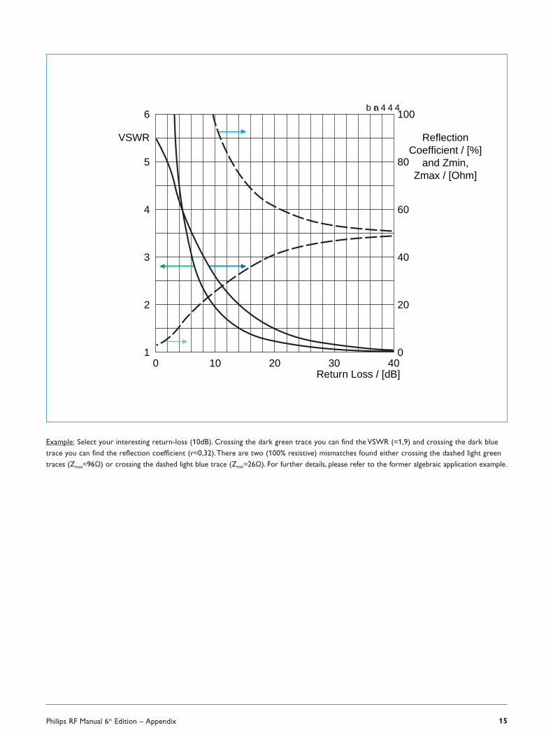
Example: Select your interesting return-loss (10dB). Crossing the dark green trace you can find the VSWR (≈1,9) and crossing the dark bluetrace you can find the reflection coefficient (r≈0,32).There are two (100% resistive) mismatches found either crossing the dashed light greentraces (Zmax≈96Ω) or crossing the dashed light blue trace (Zmin≈26Ω). For further details, please refer to the former algebraic application example.

Philips RF Manual 6th Edition – Appendix 16
2.1.3 Differences between ideal and practical passive devices
Practical devices have so-called parasitic elements at very high frequencies.
Resistor Has an inductive parasitic action and acts like a low-pass filtering function.Inductor Has a capacitive and resistive parasitic, causing it to act like a damped parallel resonant tank circuit with a certain self
resonance.Capacitor Has an inductive and resistive parasitic, causing it to act like a damped tank circuit with Series Resonance Frequency (SRF).
The inductor’s and the capacitor’s parasitic reactance causes self-resonances.
b ra 4 4
L
Cx
L Rx
Rx1
Rresistor model
capacitor model
inductor model
Cx
R Lx
C
C
Lx Rx2
Fig.7 Equivalent models of passive lumped elements
The use of a passive component above its SRF is possible, but must be critically evaluated.A capacitor above its SRF appears as an inductorwith DC blocking capabilities.
Philips RF Manual 6th Edition – Appendix 17
2.1.4 The Smith chart
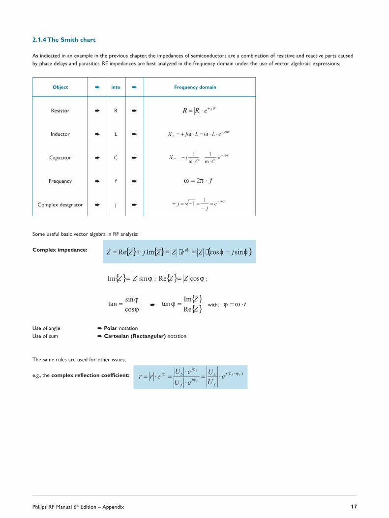
As indicated in an example in the previous chapter, the impedances of semiconductors are a combination of resistive and reactive parts causedby phase delays and parasitics. RF impedances are best analyzed in the frequency domain under the use of vector algebraic expressions:
Object into Frequency domain
Resistor R
Inductor L
Capacitor C
Frequency f
Complex designator j
Some useful basic vector algebra in RF analysis:
Complex impedance:
with;
Use of angle Polar notationUse of sum Cartesian (Rectangular) notation
The same rules are used for other issues,
e.g., the complex reflection coefficient:
( )ϕϕϕ sincosImRe jZeZZjZZ j −⋅=⋅=+=

Philips RF Manual 6th Edition – Appendix 18
Special cases:
• Resistive mismatch: reflection coefficient:
• Inductive mismatch: reflection coefficient:
• Capacitive mismatch: reflection coefficient:
The Gaussian number area (Polar Diagram) allows charting rectangular two-dimensional vectors:
Dots on the Re-Line are 100% resistiveDots on the Im-Line are 100% reactiveDots some their above the Re-Line are inductive + resistiveDots some their below the Re-Line are capacity + resistive
b ra 4 4
Im (Z)
Re (Z)
Im
180 Reresistive-axis
reactive-axis
0
Z
ϕ
Resistive-Axis
Resistive-Axis
In applications, RF designers try to remain close to a 50 Ω resistive impedance.The polar diagram’s origin is 0 Ω. In RF circuits, relatively largeimpedances can occur but we try to remain close to 50 Ω by special network design for maximum power transfer. Practically, very low andvery high impedances don’t need to be known accurately.The Polar diagram can’t show simultaneous large impedances and the 50 Ω regionwith acceptable accuracy, because of limited paper size.
b ra 4 4 7
50 Ω
2 nH
100 pF
S11
f MHzStop1000
Start10
SRF = 355.9 MHz
10 MHz0 Ω
1 GHzr = 4
a
a
r = 1
b
bcc
∞ Ω
Using this fact Mr. Phillip Smith, an engineer at Bell Laboratories,developed the so-called Smith Chart in the 1930s.The chart’s ori-gin is at 50Ω. Left and right resistive values along the real axis end in0Ω and at ?Ω.The imaginary reactive axis (imaginary axis, or Im-Axis)ends in 100% reactive (L or C). High resolution is provided close tothe 50Ω origin. Far away of the chart’s centre the resolution drops.Further from the centre of the chart, the resolution / error increases.The standard Smith Chart only displays positive resistancesand has a unit radius (r=1). Negative resistances generated byinstability (e.g. oscillation) lie outside the unit circle. In this non-linear scaled diagram, the infinite dot of the Re-Axis is ‘theoretically’bent to the zero point of the Smith Chart. Mathematically it can beshown that this will form the Smith Chart’s unit circle (r=1).All dotslying on this circle represent a reflection coefficient magnitude of 1(100% mismatch).Any positive L/C combination with a resistor willbe mathematically represented by its polar notation reflection coeffi-cient inside the Smith Chart’s unity circle. Because the Smith Chart isa transformed linear-scale polar diagram, we can use 100% of thepolar diagram rules. Cartesian-diagram rules are changed due to non-linear scaling.

Philips RF Manual 6th Edition – Appendix 19
Special cases:• Dots below the horizontal axis represent impedance with a capacitive part ( 180° < ϕ < 360° )• Dots laying on the horizontal axis (ordinate) are 100% resistive ( ϕ = 0° )• Dots laying on the vertical axis (abscissa) are 100% reactive ( ϕ = 90° )
b ra 4 4 8
0
0.2
0.6
0.4
0.8
1.0
1.0
+5
+2
+1
+0.5
+0.2
0
−0.2
−0.5
−1
−2
−5
0.2 0.5
Scaling rulefor determinethe Magnitude
(vector distance)of the reflection
coefficient
25 Ω
1 2 5180°
−135°
−90°
−45°
0°
45°
90°
135°
100 MHz
200 MHz500 MHz
1 GHz2 GHz
3 GHz
100 Ω
Z = 0 Ω Z = 0 Ω
C-Area
L-Area
L-Area
C-
Z=0 Z=∞
Fig.8: BGA2003 output Smith chart (S22)
The special cases for zero and infinitely large impedance are illustrated (above).The upper half circle is the inductive region.The lower half of the circle is the capacitive region.The origin is the 50Ω system reference (ZO).To be more flexible, numbers printed in the chart are normalized to ZO.
Normalizing impedance procedure: ZO = System reference impedance (e.g., 50Ω, 75Ω)
Example: Plot a 100Ω & 50Ω resistor into the upper BGA2003’s output Smith chart.Calculation: Znorm1=100Ω/50Ω=2; Znorm2=25Ω/50Ω=0.5Result: The 100Ω resistor appears as a dot on the horizontal axis at the location 2.
The 25Ω resistor appears as a dot on the horizontal axis at the location 0.5
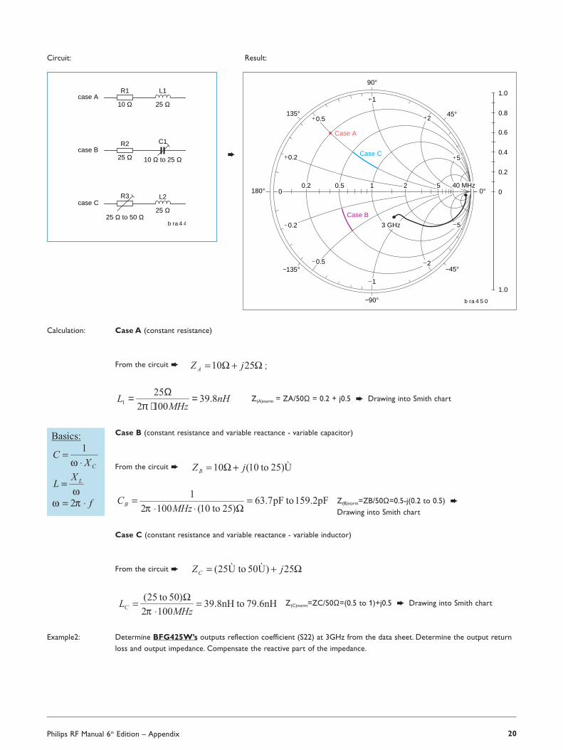
Example1: In the following three circuits, capacitors and inductors are specified by the amount of reactance @ their 100MHz designfrequency. Determine the value of the parts. Plot their impedance in to the BFG425W’s output (S22) Smith chart.
Philips RF Manual 6th Edition – Appendix 20
Circuit: Result:
b ra 4 4
R1
10 Ωcase A
L1
25 Ω
case B
case CR3
25 Ω to 50 Ω
L2
25 Ω
R2
25 Ω
C1
10 Ω to 25 Ω
b ra 4 5 0
0
0.2
0.6
0.4
0.8
1.0
1.0
5
2
1
0.5
0.2
0
0.2
0.5
1
2
5
0.2 0.5
Case A
Case C
Case B
1 2 5180°
−135°
−90°
−45°
0°
45°
90°
135°
40 MHz
3 GHz
Calculation: Case A (constant resistance)
From the circuit
Z(A)norm = ZA/50Ω = 0.2 + j0.5 Drawing into Smith chart
Case B (constant resistance and variable reactance - variable capacitor)
From the circuit
Z(B)norm=ZB/50Ω=0.5-j(0.2 to 0.5) Drawing into Smith chart
Case C (constant resistance and variable reactance - variable inductor)
From the circuit
Z(C)norm=ZC/50Ω=(0.5 to 1)+j0.5 Drawing into Smith chart
Example2: Determine BFG425W’s outputs reflection coefficient (S22) at 3GHz from the data sheet. Determine the output returnloss and output impedance. Compensate the reactive part of the impedance.
nHMHz
L 8.391002
251 =
⋅Ω=
π

Philips RF Manual 6th Edition – Appendix 21
Calculation: The data in the Smith chart can be read withimproved resolution by using the vector reflec-tion coefficient in Polar notation.
Procedure: 1) Mechanically measure the scalar length from the chart origin to the 3GHz (vector distance).2) On the chart’s right side is printed a rulerwith the numbers of 0 to 1. Read from it theequivalent scaled scalar length |r| = 0.34
3) Measure the angle ∠ (r) = ϕ = -50°.Write the reflection coefficient in vector polar notation
Normalized impedance:
Because the transistor was characterized in a50Ω bench test set-up Zo = 50Ω
Impedance:
The output of BFG425W has an equivalentcircuit of 65.2Ω with 1.38pF series capacitance.Output return loss, not compensated: RLOUT= -20log(|r|)=9.36dB resulting in VSWROUT=2
For compensation of the reactive part of theimpedance, we take the conjugate complex ofthe reactance:Xcon=-ImZ = --j38.4Ω = +j38.4Ω resulting in
A 2nH series inductor will compensate thecapacitive reactance.The new input reflectioncoefficient is calculated to:
Output return loss, compensated: RLOUT= -20log(0.132)=17.6dB resulting in VSWROUT=1.3
Please note: In practical situations the output impedance is afunction of the input circuit.The input and out-put matching circuits are defined by the stabilityrequirements, the need gain and noise-matching.Investigation is done by using network analysisbased on s-parameters.
b ra 4 5 1
0
0.2
0.6
0.4
0.8
1.0
1.0
5
2
1
1
2
5
−50
1 2 5
−90°
−45°
0°
45°
90°
40 MHz
3 GHz

Philips RF Manual 6th Edition – Appendix 22
2.2 Small signal RF amplifier parameters
2.2.1 Transistor parameters, DC to microwave
At low DC currents and voltages, one can assume a transistor acts like a voltage-controlled current source with diode clamping action in thebase-emitter input circuit. In this model, the transistor is specified by its large-signal DC-parameters, i.e., DC-current gain (B, ß, hfe), maximumpower dissipation, breakdown voltages and so forth.
b ra 4 5
rb rc
re
re' Dbe Ic = β*lb
E
CB
Thermal Voltage:VT=kT/q≈26mV@25°CICO = Collector reverse saturation current
Low frequency voltage gain
Current gain
Increasing the frequency to the audio frequency range, the transis-tor’s parameters change due to frequency-dependent phase shift andparasitic capacitance effects. For characterization of these effects,small signal h-parameters are used.These hybrid parameters aredetermined by measuring voltage and current at one terminal andusing open or short (standards) at the other port.The h-parameter matrix is shown below.
h-parameter Matrix:
Increasing the frequency to the HF and VHF ranges, open portsbecome inaccurate due to electrically stray field radiation.This resultsin unacceptable errors. Due to this phenomenon, y-parameterswere developed.They again measure voltage and current, but use onlya ‘short’ standard.This ‘short’ approach yields more accurate resultsin this frequency region. The y-parameter matrix is shown below.
y-parameter Matrix:
Further increasing the frequency, the parasitic inductance of a ‘short’causes problems due to mechanical-dependent parasitics.Additionally,measuring voltage, current and phase is quite tricky.The scatteringparameters, or s-parameters, were developed based on the measurement of the forward and backward traveling waves to deter-mine the reflection coefficients on a transistor’s terminals (or ports).The s-parameter matrix is shown below.
s-parameter Matrix:
∗
=
2
1
2221
1211
2
1
u
i
hh
hh
i
u
∗
=
2
1
2221
1211
2
1
u
u
yy
yy
i
i
∗
=
2
1
2221
1211
2
1
a
a
SS
SS
b
b

Philips RF Manual 6th Edition – Appendix 23
b ra 4 5
(s) portport
a1
b1
a2
b2
Matrix:
Equation:
2.2.2 Definition of the s-parameters
Every amplifier has an input port and an output port (a 2-port network).Typically the input port is labeled Port-1 and the output is labeled Port-2.
Fig.10:Two-port network’s (a) and (b) waves
The forward-traveling waves (a) are traveling into the DUT’s (input or output) ports.The backward-traveling waves (b) are reflected back from the DUT’s ports The expression ‘port ZO terminate’ means the use of a 50ø-standard.This is not a conjugate complex power match! In the previous chapter the reflection coefficient was defined as:
Reflection coefficient:
Calculating the input reflection factor on port 1: with the output terminated in ZO.
That means the source injects a forward-traveling wave (a1) into Port-1. No forward-traveling power (a2) injected into Port-2.The same proce-dure can be done at Port-2 with the
Output reflection factor: with the input terminated in ZO.
Gain is defined by:
The forward-traveling wave gain is calculated by the wave (b2) traveling out of Port-2 divided by the wave (a1) injected into Port-1.
The backward traveling wave gain is calculated by the wave (b1) traveling out of Port-1 divided by the wave (a2) injected into Port-2.
The normalized waves (a) and (b) are defined as:
= signal into Port-1
= signal into Port-2
= signal out of Port-1
= signal out of Port-2
Forward transmission:
Isolation:
Input return loss:
Output return loss:
Insertion loss:

Philips RF Manual 6th Edition – Appendix 24
The normalized waves have units of and are referenced to thesystem impedance ZO, shown by the following mathematical analyses:The relationship between U, P an ZO can be written as:
O
O
ZiPZ
u ⋅== Substituting: O
O
ZZ
Z =0
O
O
O
O
O Z
iZP
Z
iZ
Z
Va
2222
11111
⋅+=⋅+=
2222
1111
1
PPiZPa O +=
⋅+= Ë 11 Pa = (Ë Unit =
Ohm
VoltWatt = )
Rem:
Because , the normalized waves can be determined by the measuring the voltage of a forward-traveling wave referenced to
the system impedance constant . Directional couplers or VSWR bridges can divide the standing waves into the forward- and
backward-traveling voltage wave. (Diode) Detectors convert these waves to the Vforward and Vbackward DC voltage.After easy processing of both
DC voltages, the VSWR can be read.
A 50Ω VHF-SWR-meter built from a kit (Nuova Elettronica). It con-sists of three strip-lines.The middle line passes the main signal fromthe input to the output. The upper and lower strip-lines select a partof the forward and backward traveling waves by special electrical andmagnetic cross-coupling. Diode detectors at each coupled strip-line-end rectify the power to a DC voltage, which is passed to an exter-nal analog circuit for processing and monitoring of the VSWR.Applications include: power antenna match control, PA output powerdetector, vector voltmeter, vector network analysis,AGC, etc.Thesekinds of circuit kits are discussed in amateur radio literature and inseveral RF magazines.b ra 4 5 4
IN
Detector Vbackward
OUT
Vforward
2.2.2.1 2-Port Network definition
b ra 4 5
forward
backward
Port-1
S21
S11 S22
S12
Port-2
Input return loss
Output return loss
Forward transmission loss (insertion loss)
Reverse transmission loss (isolation)
Fig.11: S-parameters in the two-port network
Philips’ data sheet parameter Insertion power gain

Philips RF Manual 6th Edition – Appendix 25
Example: Calculate the insertion power gain for the BGA2003 at 100MHz, 450MHz, 1800MHz, and 2400MHz for the bias set-upVVS-OUT=2.5V, IVS-OUT=10mA.
Calculation: Download the s-parameter data file [2_510A3.S2P] from the Philips website page for the Silicon MMIC amplifierBGA2003.
This is a section of the file:
# MHz S MA R 50
! Freq S11 S21 S12 S22 :
100 0.58765 -9.43 21.85015 163.96 0.00555 83.961 0.9525 -7.204
400 0.43912 -28.73 16.09626 130.48 0.019843 79.704 0.80026 -22.43
500 0.39966 -32.38 14.27094 123.44 0.023928 79.598 0.75616 -25.24
1800 0.21647 -47.97 4.96451 85.877 0.07832 82.488 0.52249 -46.31
2400 0.18255 -69.08 3.89514 76.801 0.11188 80.224 0.48091 -64
Results: 100MHz 20?log(21.85015) = 26.8 dB
450MHz
1800MHz 20?log(4.96451) = 13.9 dB
2400MHz 20?log(3.89514) = 11.8 dB
2.2.2.2 3-Port Network definition
Typical products for 3-port s-parameters are: directional couplers,power splitters, combiners, and phase splitters.
Fig.12:Three-port networks (a) and (b) waves
b ra 4 5
(s) port2port1
port3
a1
a3
b1
b3
a2
b2
3-Port s-parameter definition:
• Port reflection coefficient / return loss:
Port 1
Port 2
Port 3
• Transmission gain:
Port 1=>2
Port 1=>3
Port 2=>3
Port 2=>1
Port 3=>1
Port 3=>2

Philips RF Manual 6th Edition – Appendix 26
2.3 RF amplifier design fundamentals
2.3.1 DC bias point adjustment for MMICs
S-parameters are dependent on the bias point and the frequency, as shown in the previous chapter. Consequently, s-parameter files do includethe DC bias-setting data. It’s recommended to use this setup because the s-parameter will not be valid for a different bias point.An exampleof DC bias-circuit design is illustrated with the BGU2003 for Vs=2.5V; Is=10mA.The supply voltage is chosen to be VCC=3V.
LNA DC bias setup
b ra 4 5 7
1
1
2
2
3 4
IN
IN
U1 C5
C1
C3
C2
C4 R1
R2
L1
+VCC
CONTROL
GND
CTRL
OUT
Vs+OUT
2.5 V/10 mA1.2 V/1 mA
b ra 4 5
Q4 C2C1
Rb
RcQ5
In
GND
Vp-OutCtrl
Ra
BGA2003 equivalent circuit: Q5 is the main RF transistor. Q4 formsa current mirror with Q5.The input current of this current mirror isdetermined by the current into Ctrl.pin. Rb limits the current when acontrol voltage is applied directly to the Ctrl input. RC, C1, and C2decouple the bias circuit from the RF input signal. Because Q4 and Q5are located on the same die, Q5’s bias point is very temperature-stable.
DC bias point adjustment for transistors
b ra 4 5
0 0.5
0.5
1
1.5
2
1 1.5 2102030IVS-OUT (mA) VCTRL (V)
ICTRL (mA)From the BGA2003 datasheet, Figs 4 and 5 were combined (see adjacent graph) to better illustrate the MMIC’s I/O DCrelationship.
The red line shows the graphical con-struction starting with the requirement ofIVS-OUT=10mA, automatically crossing theordinate ICTRL=1mA, and finishing intothe abscissa at VCTRL=1.2V
2.3.2 DC bias point adjustment for transistors
In contrast to the easy bias setup for MMICs, here is the design of a setup used, for example, in audio or IF amplifiers.
URCURB
b ra 4 6
IN
RB
IbIc
RC
C1
VCC
OUT
Q1
UBE
UCE

Philips RF Manual 6th Edition – Appendix 27
DC bias setup with stabilization via voltage feedbackThe advantage of this setup is a very highly resistive, resistor RB. Its lowering of the input impedance at terminal [IN] can be negated, and theIF-band filter is less loaded. Because there is no emitter feedback resistor, high gain is achieved from Q1.This is needed for narrow bandwidth,high-gain IF amplifiers.The disadvantage is a very low stability of the operating point caused by the Si BE-diodes’ relatively linear negative
temperature coefficient of ca.VBE≈ -2.5mV/K into amplified
This can be lowered by adding an extra resistor between ground and the emitter.
bra461
L9
C11
C1
L8
L2
L3 L5
L4
L1
C10
C14, C15,C16
C12 C13
C2, C3,C4, C5
C6, C7,C8
R1 T1
R2
L10
Vbias
50 Ωinput
50 Ωoutput
C9DUT
L6
L7
VS
An emitter resistor has the disadvantage of gain loss or the need fora bypassing capacitor.Additionally, the transistor will loose quality inits gnd performance (instability) and will have an emitter heat sinkinginto the gnd plane.At medium output power, the bias setup must bestabilized due to the increased junction temperature causing DCdrifting.Without stabilization the transistor will burn out or distortioncan rise.A possible solution is illustrated in the adjacent picture(BFG10). Comparable to the BGA2003, a current mirror is designedtogether with the DC transistor T1.T1 works like a diode with a VCE
(VBE) drift close to the RF transistor (DUT) in the case of close thermalcoupling.With ‚β1=βDUT and VBE-1≈VBE-DUT we can do a very simplifiedalgebraic analysis:
finalizing into a very temperature-independent relation ship of IC-DUT ≈ IC1 ≈ (Vbias-VBE)/R2 For best current imaging, the BE diestructure areas should have similar dimensions.
2.3.3 Gain definitions
The gain of an amplifier is specified in several ways depending on how the (theoretical) measurement is implemented, on stability conditions,and on way of matching (e.g. best power processing, max. gain, lowest noise figure or a certain stability performance). Often certain powergains are calculated for the upper and lower possible parameter extremes.Additionally calculating circles in the smith chart (power gain circles,stability circles) can be used to select a useful working range in the input or output.The algebraic expressions used can vary from one literaturesource to the other. In reality S12 cannot be neglected, causing the output being a function of the required source and the input being a functionof the required load.This makes matching complicated and is a part of the GA and GP design procedure.
Transducer power gain:
This includes the effect of I/O matching and device gain but doesn’t take into account the losses in components.
Power gain or operating power gain:
Used in the case of non-negligible S12, GP is independent of the source impedance.
Available power gain:
GA is independent of the load impedance.

Philips RF Manual 6th Edition – Appendix 28
Maximum available gain (MAG):
The MAG you could ever hope to get from a transistor is under simultaneous conjugated I/O match with a Rollett stability factor of K>1.K is calculated from the s-parameters in several sub steps.At a frequency of unconditional stability, MAG (GT,max=GP,max=GA,max) is plotted intransistor data sheets.
Maximum stable gain:
MSG is a figure of merit for a potentially unstable transistor and valid for K=1 (subset of MAG).At a frequency of potential instability, MSG isplotted in transistor data sheets.
Further examples of used definitions in the design of amplifiers:- GT,max = Maximum transducer power gain under simultaneous conjugated match conditions- GT,min = Minimum transducer power gain under simultaneous conjugated match conditions- GTU = Unilateral transducer power gain- GP,min = Minimum operating power gain for potential unstable devices
- Unilateral figure of merit determine the error caused by assuming S12=0.
The adjacent example shows the BGU2003’s gain as a function of frequency
In the frequency range of 100 MHz to 1 GHz the MMIC is potentiallyunstable.Above 1.2 GHz the MMIC is unconditionally stable (withinthe 3 GHz range of measurement)
GUM is the maximum unilateral transducer power gain assuming S12=0and a conjugated I/O match:A S12=0 (=unilateral figure of merit)specify an unilateral 2-port network resulting in K=infinite and DS=S11*S22
For further details please refer to books e.g. Pozar, Gonzalez, Bowick, etc.
f (MHz)102 104103
bra462
20
10
30
40
gain(dB)
0
MSG
Gmax
GUM
2.3.4 Amplifier stability
All variables must be processed with complex data.The evaluated K-factor is only valid for the frequency and bias setup for the selecteds-parameter quartet [S11, S12, S21, S22]
Determinant:
Rollett stability factor:

Philips RF Manual 6th Edition – Appendix 29
References — RF Application - Basics & Design - Basics1. Philips Semiconductors, RF Wideband Transistors and MMICs, Data Handbook SC14 2000, S-parameter Definitions, page 39 2. Philips Semiconductors, Datasheet, 1998 Mar 11, Product Specification, BFG425W, NPN 25GHz wideband transistor 3. Philips Semiconductors, Datasheet, 1999 Jul 23, Product Specification, BGA2003, Silicon MMIC amplifier 4. Philips Semiconductors, Datasheet, 2000 Dec 04, Product Specification, BGA2022, MMIC mixer 5. Philips Semiconductors, Datasheet, 2001 Oct 19, Product Specification, BGA2711, MMIC wideband amplifier 6. Philips Semiconductors, Datasheet, 1995 Aug 31, Product Specification, BFG10; BFG10/X, NPN 2GHz RF power transistor7. Philips Semiconductors, Datasheet, 2002 May 17, Product Specification, BGU2703, SiGe MMIC amplifier8. Philips Semiconductors, Discrete Semiconductors, FACT SHEET NIJ004, Double Polysilicon – the technology behind silicon MMICs,
RF transistors & PA modules 9. Philips Semiconductors, Hamburg, Germany,T. Bluhm,Application Note, Breakthrough In Small Signal - Low VCEsat (BISS) Transistors
and their Applications,AN10116-02, 2002 10. H.R. Camenzind, Circuit Design for Integrated Electronics, page34, 1968,Addison-Wesley,11. Prof. Dr.-Ing. K. Schmitt,Telekom Fachhochschule Dieburg, Hochfrequenztechnik 12. C. Bowick, RF Circuit Design, page 10-15, 1982, Newnes13. Nührmann,Transistor-Praxis, page 25-30, 1986, Franzis-Verlag14. U.Tietze, Ch. Schenk, Halbleiter-Schaltungstechnik, page 29, 1993, Springer-Verlag15. W. Hofacker,TBB1,Transistor-Berechnungs- und Bauanleitungs-Handbuch, Band1, page 281-284, 1981, ING.W. HOFACKER16. MicroSim Corporation, MicroSim Schematics Evaluation Version 8.0, PSpice, July 199817. Karl H. Hille, DL1VU, Der Dipol in Theorie und Praxis, Funkamateur-Bibliothek, 199518. PUFF, Computer Aided Design for Microwave Integrated Circuits, California Institute of Technology, 199119. Martin Schulte, ‘Das Licht als Informationsträger’,Astrophysik, 07.Feb. 2001,Astrophysik%20Teil%201%20.pdf20. http://www.microwaves101.com/encyclopedia/basicconcepts.cfm21. http://www.k5rmg.org/bands.html22. http://www.unki.de/schulcd/physik/radar.htm23. SETI@home, http://www.planetary.org/html/UPDATES/seti/SETI@home/Update_022002.htm
http://www.naic.edu/about/ao/telefact.htm24. Kathrein, Dipl. Ing. Peter Scholz, Mobilfunk-Antennentechnik.pdf, log.-per.Antenne K7323225. Siemens Online Lexikon26. http://wikipedia.t-st.de/data/Frequenzband27. www.wer-weiss-was.de/theme134/article1180346.html28. www.atcnea.at/flusitechnik/themen1/radartechnik-grundlagen.html29. Nührmann, Das große Werkbuch Elektronik,Teil A, 5.Auflage, Franzis-Verlag, 198930. ARRL,American Radio Relay League
In some literature sources, the size of DS isn’t take into account for dividing into the following stability qualities.
K>1 & |Ds|<1Unconditionally stable for any combination of source and load impedance
K<1Potentially unstable and will most likely oscillate with certain combinations of source and load impedance. It does not mean that the transistorwill not be useable for the application. It means the transistor is more tricky to use.A simultaneous conjugated match for the I/O isn’t possible.
-1<K<0Used in oscillator designs
K>1 & |Ds|>1This potentially unstable transistors with the need SWR(IN)=SWR(OUT)=1 are not manufactured and do have a gain of GT,min.
Philips RF Manual 6th Edition – Appendix 30
3. Introduction to noise
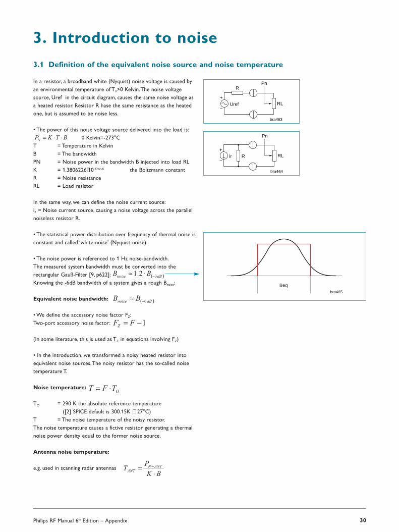
3.1 Definition of the equivalent noise source and noise temperature
In a resistor, a broadband white (Nyquist) noise voltage is caused byan environmental temperature of TU>0 Kelvin.The noise voltagesource, Uref in the circuit diagram, causes the same noise voltage asa heated resistor. Resistor R hase the same resistance as the heatedone, but is assumed to be noise less.
• The power of this noise voltage source delivered into the load is:0 Kelvin=-273°C
T = Temperature in KelvinB = The bandwidthPN = Noise power in the bandwidth B injected into load RLK = 1.3806226⋅10-23Ws/K the Boltzmann constantR = Noise resistanceRL = Load resistor
In the same way, we can define the noise current source:iR = Noise current source, causing a noise voltage across the parallelnoiseless resistor R.
• The statistical power distribution over frequency of thermal noise isconstant and called ‘white-noise’ (Nyquist-noise).
• The noise power is referenced to 1 Hz noise-bandwidth.The measured system bandwidth must be converted into the rectangular Gauß-Filter [9, p622]:Knowing the -6dB bandwidth of a system gives a rough Bnoise:
Equivalent noise bandwidth:
• We define the accessory noise factor FZ:Two-port accessory noise factor:
(In some literature, this is used as TZ in equations involving FZ)
• In the introduction, we transformed a noisy heated resistor intoequivalent noise sources.The noisy resistor has the so-called noisetemperature T.
Noise temperature:
TO = 290 K the absolute reference temperature([2] SPICE default is 300.15K ≅ 27°C)
T = The noise temperature of the noisy resistor.The noise temperature causes a fictive resistor generating a thermalnoise power density equal to the former noise source.
Antenna noise temperature:
e.g. used in scanning radar antennas
bra463
R
+
−
Pn
RLUref
bra464
R+
−
Pn
RLir
bra465
Beq

Philips RF Manual 6th Edition – Appendix 31
3.2 Determine the equivalent noise sources
Normally, power matches are used in RF designs:
(1) and (2)
At power match, the voltage delivered to the load is the half of thegenerator quantity and the delivered current is the half of the shuntedsource, resulting in the maximum power delivered into the load.Maximum current IL(max) (current match) is found at RL=0 generating
This P0 100% grilled in Rg. Maximum available power from the source
is found at RL=Rg with . PRg=P0-PL is burned by Rg.
R
UIUPPL
2
0000
4
1
222⋅=⋅==
LL RPU ⋅⋅= 40
LL
LL
L RPRPU
U ⋅=⋅⋅
==2
4
2
0
LL UU ⋅= 2ˆ
LLL RBTKU ⋅⋅⋅⋅= 2ˆ
LNL RBTKU ⋅⋅⋅⋅= 2ˆ
NN RBTKU ⋅⋅⋅⋅= 40
(3) with U0 and I0 in RMS quantity
(4)
(5) RMS load noise voltage; UL=0.5*U0 valid for power match
(6)
(7) At power match: RN=RL consequently TN=TL
(8)Noise peak-voltage across the load
(9) RMS voltage of the equivalent noise source’s generator
In the introduction, we mentioned UL dependence on the shunt, open and matched source.This indicates that the noise available into a two-portis a function of the return loss (load and source impedance relationship). In LNAs, the input impedance must be matched to the equivalentnoise-source impedance specified in the datasheets by the characteristic noise-parameters. For cascaded amplifiers, typically the rating of thenoise-figure or noise temperature for the ideal (noise matched) condition is given.A mismatch is a noise-source too.This mismatch can be seenas a loss of delivered power into a two-port. Furthermore, loss of power can be caused in e.g. a resistive power attenuator. At such attenuatorbuilding blocks, the noise-figure is identical to the attenuation (explained in a later chapter).
The resulting equation (12) is confirmed by [10, p161] but without explanations and algebraic rooting.
Some literature e.g. for operational amplifiers, uses the unit expressions and
Normalized to a 1 Hz bandwidth gives the bandwidth independent normalized noise voltage quantity:
for simplification the comparison of noise performances measured under different conditions andapplications.NN RTKHzU ⋅⋅⋅= 40

Philips RF Manual 6th Edition – Appendix 32
A two-port device (amplifier, attenuator, detector, filter), just loadedwith the characteristic impedances at the input and output, generatesan outgoing noise power towards the load RL without any two-portinput signal.This noise power is found at a temperature TU>0K.Replacing the input-matching resistor by a source shows that thisnoise power adds to the device’s output signal as shown in the diagram.The noise power Pan is caused by the amplifier itself (e.g. semiconductor noise)
There is
Pon = Sum of all noise power out of the two-portPin = Noise power caused by the input sourcePan = Additional noise power caused by the two-port itselff(PI) = Two-port transfer-function (=frequency-dependent gain)
bra467
Po
+
−
PiPis and Pin
Pan
Po = f(Pi)Pos and Pon
Noise-Factor:
Signal to Noise Ratio:
Gn = Noise gainGs = Signal gain
Noise Figure:
Two-port’s equivalent noise temperature
can be found from the noise factor by:
vice versus
The expression noise temperature is used in e.g. extremely low noise amplifiers like Radar applications (amplifier, antenna), in cooled CCD-image cameras, in infrared-emission-microscopes (used in failure analysis labs for investigating semiconductors), in infrared cameras, etc.The cooling is made by Peltier elements down to about -50°C or by liquid nitrogen down to about -196°C.
Ratio Noise toSignalOutput
Ratio Noise toSignalInput
)(
)( ==OUT
IN
SNR
SNRF
in
isIN
P
PSNR =)(
on
osOUT
P
PSNR =)(
s
n
is
os
in
on
in
on
os
is
on
os
in
is
OUT
IN
G
G
P
P
P
P
P
P
P
P
P
P
P
P
SNR
SNRF ==⋅===
)(
)( sn GFG ⋅=
3.3 Noisy two-port device: the noise figure and SNR
acc. [23]
SNR / [dB] Quality
0 MDS = minimum detectable signal
10 Minimal quality for understanding of voice
20 Good quality of understanding the voice
30 Minimum quality need for music
Philips RF Manual 6th Edition – Appendix 33
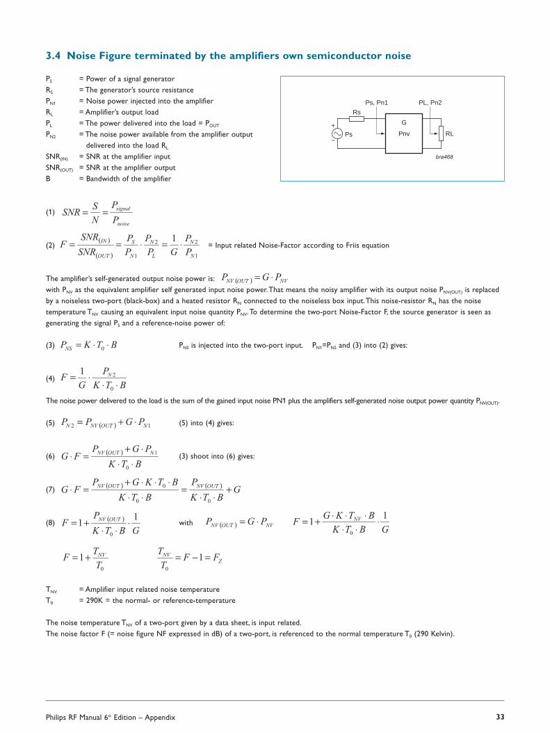
3.4 Noise Figure terminated by the amplifiers own semiconductor noise
PS = Power of a signal generatorRS = The generator’s source resistancePN1 = Noise power injected into the amplifierRL = Amplifier’s output loadPL = The power delivered into the load = POUT
PN2 = The noise power available from the amplifier output delivered into the load RL
SNR(IN) = SNR at the amplifier inputSNR(OUT) = SNR at the amplifier outputB = Bandwidth of the amplifier
(1)
(2) = Input related Noise-Factor according to Friis equation
The amplifier’s self-generated output noise power is:with PNV as the equivalent amplifier self generated input noise power.That means the noisy amplifier with its output noise PNV(OUT) is replacedby a noiseless two-port (black-box) and a heated resistor RN connected to the noiseless box input.This noise-resistor RN has the noise temperature TNV causing an equivalent input noise quantity PNV.To determine the two-port Noise-Factor F, the source generator is seen asgenerating the signal PS and a reference-noise power of:
(3) PNS is injected into the two-port input. PN1=PNS and (3) into (2) gives:
(4)
The noise power delivered to the load is the sum of the gained input noise PN1 plus the amplifiers self-generated noise output power quantity PNV(OUT).
(5) (5) into (4) gives:
(6) (3) shoot into (6) gives:
(7)
(8) with
TNV = Amplifier input related noise temperatureT0 = 290K = the normal- or reference-temperature
The noise temperature TNV of a two-port given by a data sheet, is input related.The noise factor F (= noise figure NF expressed in dB) of a two-port, is referenced to the normal temperature T0 (290 Kelvin).
G
Pnv
bra468
Rs
+
−
PL, Pn2
RLPs
Ps, Pn1
Philips RF Manual 6th Edition – Appendix 34
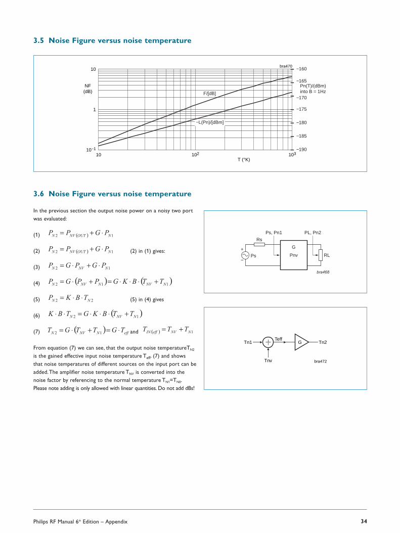
3.5 Noise Figure versus noise temperature
bra470
T (°K)10 103102
1
10
NF(dB)
10−1
Pn(T)/(dBm)into B = 1Hz
−160
−165
−170
−175
−180
−185
−190
F/[dB]
−L(Pn)/[dBm]
3.6 Noise Figure versus noise temperature
In the previous section the output noise power on a noisy two portwas evaluated:
(1)
(2) (2) in (1) gives:
(3)
(4)
(5) (5) in (4) gives
(6)
(7) and
From equation (7) we can see, that the output noise temperatureTN2
is the gained effective input noise temperature Teff. (7) and showsthat noise temperatures of different sources on the input port can beadded.The amplifier noise temperature TNV is converted into thenoise factor by referencing to the normal temperature TN1=TN0.Please note adding is only allowed with linear quantities. Do not add dBs!
G
Pnv
bra468
Rs
+
−
PL, Pn2
RLPs
Ps, Pn1
bra472
GTn1 Tn2
Tnv
Teff
Philips RF Manual 6th Edition – Appendix 35
3.7 Noise temperature of a lossy device (attenuator, cable etc.)
The attenuator is a two-port with the gain: (1) D= Attenuation factor
Its noise factor is: (2) (for details refer to previous chapters)
Because the Friis Noise-Factor is referenced to T0: (3)
The attenuator is a passive two-port. It does not generate additional pink-noise into the pass-band bandwidth B, as happens in a semiconductordevice. Due to its resistive behavior working on the system impedance Z0, the output Nyquist noise power is: (4)
(3) and (4) into (2) gives: (5)
For an attenuator with a temperature TATN=T0 follows the noise factor:
From the definition is found
That means e.g. a cable in a system adds white noise, modeled by a noise factor equal to the damping (attenuation) factor D. For example,a filter with 3 dB insertion-loss has a noise figure of NF = 3 dB.
This behavior can be explained in the following practical way too:An ideal signal generator injects a clean signal into the attenuator.This signal generator has the impedance Z0 heated with the temperature T0 causing a certain SNR(IN) referenced to the system Z0 noise power N0.The attenuator drops down the signal power by its attenuation.The attenuator does not create self-noise power but its output is again referenced to Z0 causing the equal reference noise power N0, becauseonly the signal power is changed by the attenuation factor by the same, N0 at the input and output ( S(in)=D*S(out); N(in)=N(out) )
for linear quantity [u]
At a resistively lossy two-port: (6) for quantity in [dB]
At a two-port is defined: (7) for quantity in [dB]
Subtracting (6) - (7) gives again: NF=Losses in [dB]
Cables and attenuators are sources of white noise!
The problem of noise caused by resistive loss is valid for a lot of circuits, like passive filters, resonators used in oscillators, strip-lines, and so on.In strip-lines, there are frequency-dependent conductive losses and dielectric losses. In some CAD programs, these can be separately defined.
3.8 Noise temperature of a resistor
The noise temperature of a resistor is equal to its body temperature. Its noise factor is

Philips RF Manual 6th Edition – Appendix 36
3.9 Cascading noisy blocks
(1) (2)
(1) in (2) gives
(3) (4)
(5)
(6)
This is equal to an amplifier (eff. gain = G1·G2) with its own equal input noise temperature TNV1+TNV2/G1.TN1 is the reference temperature injected into the cascaded amplifier to determine the Friis Noise factor.
The resulting amplifier noise temperature of a cascaded amplifier results in:
(7)
(8) (8) into (7) results in the effective system access noise factor.T0 can be canceled out.
(9).
(10) (11)
The resulting effective system noise factor becomes:
(12) Noise Figure: (13)
3.10 Example: a main satellite receiver system design
A receiver system ( TSYS(eff) ) is build by a dish (TANT) with built-in LNA (G1;TLNA), followed by a lossy cable (damping factor Dcabel=1/G2;temperature Tcabel) ending in the SAT receiver (G3;TSATR):
Scheme of cascading noise temperatures: (0) Applied to the present case:
(1) (TANT=TN1 from the previous section)
bra473
GTn2
Tn3
Tnv2
Teff2GTn1
Tnv1
Teff1

Philips RF Manual 6th Edition – Appendix 37
(2)
Noise factor of the cable is (3)
(4)
The resulting input-related noise temperature of the satellite system is:
(5) (in linear quantity [u])
The effective system noise figure is: (6) (antenna dish included)
For a certain allowed maximum bit error rate BER (demodulated signal) at the baseband processor output, the equivalent min basebandSNR(SATRBB) can be determined.The relationship for BER versus SNR depends on the modulation used.The SNR(ANT) at the dish input must bebetter by at least the factor FSYS(eff).
(7) (in linear quantity [u])
The effective noise power at the SAT-dish can be determined by: (8)
The min. signal for operation is then easily found by: (9)
An antenna signal power of >PSant(min) ensures the min. BER in the SAT-receiver’s baseband processor, and this quantity appears to be theSAT-system sensitivity for the requested BER.
The level of the noise floor at the baseband processor output is given by: (10)
In [25, p8] the BER is given as a function of SNR by … ‘the Defense Science and Technology Organization (DSTO) to support the ModernizedHigh Frequency Communications System (MHFCS) [1], (also referred to by its project nomenclature JP2043), to be built to serve the AustralianDefense Force.’... ‘This work covers a wide range of topics including characterization of expected HF noise and channel distortion, waveformdesign, protocol design, radio access scheme design, provision of HF Internet services, overall system design, and modeling and simulation ofend-user service performance. ...’
bra474
SNR in 3 kHz Channel (dB)−10 503010
10−3
10−4
10−1
10−2
1Bit-Error
Rate
10−5
1 - Turbo-Coded Chirp, 75 bps, 64 s int.2 - Conv.-Coded Chirp, 75 bps, 64 s int.3 - TCM-16, 300 bps, 20 s int.4 - TCM-16, 600 bps, 20 s int.5 - TCM-16, 1200 bps, 20 s int.6 - TCM-16, 2400 bps, 20 s int.7 - 52-tone, 4800 bps, 30 s interleaving8 - Single-tone (std), 2400 bps, 9.6 s int.9 - Single-tone, 3200 bps, 9.6 s int.10- Single-tone, 4800 bps, 9.6 s int.
1 2 3 4 5 6
78910

3.11 Antenna noise
Antenna noise is sometimes called sky noise.The antenna receives noise from several sources [20, p5]:
• Terrestrial noise (man-made noise) sources• Solar noise sources• Galactic sources• Noise caused by the antenna radiation food impedance
The size of the noise source depends on the antenna elevation angle, time of day, sun activity, and the frequency.These noises are modeled as an increased thermal-noise temperature of the antenna.
Philips RF Manual 6th Edition – Appendix 38
[21, p2] says ‘antennas radiate broadband ‘blackbody’ noise corresponding to their surface temperature. If the beam of an antennais narrower than the noise’, it ‘sees’ the background with noise temperature Tb=290k.A satellite dish aimed at the earth surface onlyreceiving the earth’s surface black body noise will have an antennatemperature of TANT=290K. If the antenna’s beam loop sees only theearth’s noise, the effective antenna temperature is the rated sharesum of all responsible temperature noise sources in the main loop:
Example for TSKY is given in the upper table.
The International Telecommunication Union (ITU) has defined (in the CCIR report 322) the frequency dependent atmospheric interferencesand (in CCIR report 258-4) man-made noise.
For further details see at e.g.:http://www.veron.nl/tech/noise/noiserefs.htmhttp://www.spawar.navy.mil/sti/publications/pubs/td/2813/nradtd2813homepg.html
Frequency Range Sky temperature Root cause30KHz - 300KHz >108K Very high atmospheric noise300KHz - 3MHz >108K High atmospheric noise3MHz - 30MHz 108 - 105K Atmospheric noise30MHz - 300MHZ 105 - 103K High Galactic noise300MHz - 3GHz 103 - 10K Galactic noise and cosmic background noise3GHz - 30GHz 10 - 100K Atmospheric thermal noise, O2, H2O resonance<30MHz Noise due to lighting discharges or ‘atmospherics’30MHz to 1GHz Galactic or cosmic noise1GHz to 10GHz Noise is generated in the atmosphere.A vertical antenna will receive less noise than a horizontal antenna.
The sky noise temperature can approach the minimum of 3K set by cosmic background radiation (relic of the ‘Big Bang’)
2GHz to 8GHz The low-noise window used in radio-telescopes and space telemetry>10GHz The noise temperature rises in peaks due to resonance effects in water vapor and oxygen molecules
(O2 H2O resonance), finally reaching a steady value of around 290Kelvin.
bra475
Zenith
Horizon
Elevationangleθ f (GHz)
0 907040 6010 30 50 8020
bra476
100
200
300
TB(K)
0H2O O2
θ = 0°
θ = 5°
θ = 10°
θ = 90°

Philips RF Manual 6th Edition – Appendix 39
According to [24, p5-6]: The statistical behavior of the antenna noisefactor, Fa, can be shown by plotting the distribution on a normalprobability graph where random variables that are Gaussian distributed form a straight line with a slope equal to its standarddeviation and a median equal to its mean.The graph is used to determine the median antenna noise figure Fam of a rural, residential,or business environment. Further analysis of Fa includes determiningwithin-the-hour-, hour-to-hour-, and location-to-location-variability.’
F is the measured noise factorFr is the receiver noise factorFa is the antenna noise factor
Adjacent is the average interference power produced by man-maderadiation, received by a short vertical antenna with ideal GND earth[26, p5] (acc. ITU-R P.372-7 ‘Radio noise’, Figure 10)
Fam in dBf in MHz
3.12 Example: A radar system
Antenna: TQ=350kReceiver: TV=380kBandwidth: BW=1MHzGain: G=100dBBaseband: SNR(OUT)=10dB
Effective system input related temperature:
The noise temperatures can be un-weighted added, because Tq
is a source.
Tv=Amplifier Tq=Antenna
Frequency (MHz)0.1 10001001 10
bra493
40
80
120
Fam(dB above
KT0b)
0
Night
Day
Galactic
BusinessResidentialRural
Atmospheric
Quiet Rural
bra478
40
60
20
80
100
Fam(dB)
0
f (MHz)10−1 1031021 10
ABCDE
bra479
Tv
SNR(OUT)Tq
Environment c dBusiness area (trace A) 76.8 27.7Residual area (trace B) 72.5 27.7Countrified area (trace C) 67.2 27.7Calm countrified area (trace D) 53.6 28.6Galactic noise (trace E) 52 23

Philips RF Manual 6th Edition – Appendix 40
13.2dB
-96.8dBm
3.13 Input and output related noise temperature
Available is the effective input noise temperature Teff of an amplifier. Its Teff is the sum of the sourcenoise temperature Tsource and the amplifier itself generate equivalent input noise temperature TV.
Teff is the sum of all system related noise sources referenced to the noise free gain block.This gain block was made noise free by using the equivalent input related noise temperature TV.The output related effective noise temperature is:
for the equivalent gain block with NF=0dB.The effective output noise power is:
with G as the gain of the amplifier.
3.14 Amplifier sourced by a noisy generator
bra480
+
−Signal
Noise signal generator
SNR(g)Png ToutRngNF, Tv
Amplifier
Tg
+
−Noise
Ps
G
bra481
+
−Noise(eff)
Pneff
SNR(out)
RneffTeff+
−Signal
ToutPsPnoutPsout
SNR(in)
Converted system
NF = 0
Amplifier
G

Philips RF Manual 6th Edition – Appendix 41
3.15 Noise Figure, noise temperature & sensitivity of a receiver
The equivalent noise temperature of a two-port (e.g. receiver) is Te.The Noise factor F of the two-port (four pole device) isdetermined by referring to the reference temperature (room temperature) of typically 290K (sometimes 300k).
(1) (2)
Te is the temperature of the theoretically resistor causing the same two-port output noise power than the noisy two-port it self.The noise power into 1 Hz bandwidth is:
-174dBm
A receiver with a noise figure NF (in dB) does have an equivalent input related noise power of:
This is called the receivers noise floor.The term ‘ + NF ‘ in the equation comes from the SNR’s definition:
A minimum detectable signal MDS must at least break through the receivers noise floor: MDS=PNiRec
Third order intermodulation-free dynamic range, IMD3, is the range where a signal can be processed and detected without distortion:
in dBm
In analog to digital converters (ADCs) the term spurious free dynamic range (SFDR) is used too.The noise floor in ADCs is evaluated from the binary resolution terminated quasi-random quantization noise.That means an ADC does have a noise figuretoo.This NF causes an ADC output signal to noise relation SNR(OUT)=SNR(IN)-NF in dB.This is used for receiver system analysis with a digital baseband processing DSP.The ADC can either sit behind the demodulator or (at modern designs) in theend of the IF rail replacing the analog demodulator.
In some literature, the term noise floor power density (NFPD) is used.That’s the equivalent noise temperature terminatedreceivers noise floor in a theoretically 1 Hz wide Gauß-filter.
in dBm
in dBm
3.16 Noise sources in semiconductor devices
The noise source can be defined by the noise figure:
Noise voltage source: Noise current source:
Ur2 and Ir2 are the square quantity of the equivalent noise sources [2].R is the noise source’s generator resistance.
u and i come out of the relation: with we do get
The amount of noise power delivered into the load is different, because of power matching the current and thevoltage; each one is the half quantity:

Philips RF Manual 6th Edition – Appendix 42
Noise source current:
Noise source voltage:
Effective noise voltage: unit [V2]
Power noise spectral density:
Voltage noise spectral density: unit [V2/HZ] [5]
Equivalent noise voltage: unit [V/√Hz] [5]
Current noise spectral density:
Noise spectra:
Shot noise: NF = model parameter
Shot noise current: caused in a PN junction [33, p42]
Short noise voltage: for rPN ref. to [34, p77]
rPN=dynamic junction impedance (base emitter diode)
Electron charge: e=q=1.6·10-19Coulombs; 1C=1J/Kelvin
Transistor forward transconductance: (small signal):
Generation-recombination noise: KB, AB, FB = model parameters
The generation-recombination noise is alternatively called combination-, recombination-, burst- or popcorn-noise.
Flicker noise: AF, KF, b=model parameter ‘B’
Normally B=1
Sometimes the Shot noise and the Flicker noise are called excess noise.
Flicker noise current: [34, p44-45]
Flicker Noise = 1/f noise

Philips RF Manual 6th Edition – Appendix 43
A coarse model of the heterodyned 1st order flick noise (1/f-noise) and broadband white noise versus frequency is given by [10, p149]:
fC = Flicker noise corner frequency
White noise is:
The diagram shows the noise power versus frequency for e.g. a transistor.In oscillators this noise distribution envelopes the carrier.
More accurate modeling is used by a higher order polynomial power density equation [10, p149]:
FM random walk noise: (1/δf4)
FM flicker noise: (1/δf3)
Random walk noise & white FM noise: (1/δf2)
PM Flicker noise: (1/δf1)
White Nyquist noise floor: (1/δf0)
Root cause of the different noise envelope selections:
PM noise in a resonator causes an FM-modulation with a 1/f2 frequency response.This 1/f2 FM modulation can be converted back into a PMmodulation with 1/f3 trace.Temperature instability and microphonic (mechanical) noise cause the so-called random walk noise with 1/f2 noisesidebands.This can be converted into 1/f3 FM noise.
According to [19, p250-252]
bra482
white noise
fc
f
1/f flicker noise
bra483
1/df^4
dP/df
1/df^3
1/df^1
1/df^2
1/df^0
f
Spectrum Name Root causeenvelope tangent1/f4 Random walk FM External physical environment influencing the oscillator. mechanical shock, vibration, temperature, …1/f3 Flicker FM Physical resonance mechanism of the active oscillator, the design or choice of parts used for electronic,
power supply or environmental properties. In high quality oscillators marked by 1/f 2 or 1/f noise.1/f2 White FM White frequency, random walk of frequency. Noise in passive-resonator frequency standards like cesium
and rubidium frequency standards1/f1 Flicker φM Flicker modulation of phase. Common in high-quality oscillators. Introduced by next-stage noisy
electronics.Amplifiers for gain the oscillator carrier or multiplier.1/f0 White φM Produced in the same way like Flicker φM.The late amplifier stage is usually responsible.
Narrow-band filter at the output can help.
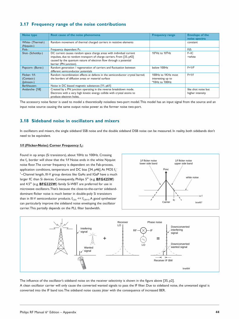
Philips RF Manual 6th Edition – Appendix 44
3.17 Frequency range of the noise contributions
The accessory noise factor is used to model a theoretically noiseless two-port model.This model has an input signal from the source and aninput noise source causing the same output noise power as the former noise two-port.
3.18 Sideband noise in oscillators and mixers
In oscillators and mixers, the single sideband SSB noise and the double sideband DSB noise can be measured. In reality, both sidebands don’tneed to be equivalent.
1/f (Flicker-Noise) Corner Frequency fC:
Found in op amps (Si transistors), about 10Hz to 100Hz. Crossing the fC border will show that the 1/f Noise ends in the white Nyquistnoise floor.The corner frequency is dependent on the Fab-process,application conditions, temperature and DC bias [34, p46].At MOS fC
-
1~Channel length, III-V group devices like GaAs and IGaP have a muchlarger fC than Si devices. Consequently, Philips 5th (e.g. BFG425W)and 4.5th (e.g. BFG325W) family Si-WBT are preferred for use inmicrowave oscillators.That’s because the close-to-the-carrier sideband-dominant flicker noise is much better in double-poly Si transistorsthan in III-V semiconductor products. fC(Si) << fC(III-V).A good synthesizercan particularly improve the sideband noise enveloping the oscillatorcarrier.This partially depends on the PLL filter bandwidth.
The influence of the oscillator’s sideband noise on the receiver selectivity is shown in the figure above [35, p2].A clean oscillator carrier will only cause the converted wanted signals to pass the IF filter. Due to sideband noise, the unwanted signal isconverted into the IF band too.The sideband noise causes jitter with the consequence of increased BER.
Noise type Root cause of the noise phenomena Frequency range Envelope of the noise spectra
White- (Thermal-) Random movement of thermal charged carriers in resistive elements constant(Nyquist-)Pink- Frequency dependent PN F(f)Shot- (Schottky-) DC current causes random space charge areas with individual current 104Hz to 109Hz F~IC
impulses, due to random transport of charge carriers. From [33, p42] ≈whitecaused by the quantum nature of electron flow through a potential barrier (PN junction).
Popcorn- (Burst-) Random generation / regeneration of carriers and fluctuation between below 100Hz F=1/f2
different semiconductor potentialsFlicker- 1/f- Random recombination effects at defects in the semiconductor crystal barred; 100Hz to 1KHz most F=1/f(Contact-) the borders of diffusion areas or material surface interesting up to (Johnson-) ª10Hz to 100HzBarkhausen- Noise in DC biased magnetic substances [11, p61]Avalanche- [18] Created by a PN junction operating in the reverse breakdown mode. like shot noise but
Electrons with a very high kinetic energy collide with crystal atoms to higher intensityproduce electron holes.
bra487
Posc
white noise
1/f flicker noiseupper side band
1/f flicker noiselower side band
f
fcCarrier
bra484
ReceiverLO Downconverted
interferingsignal
Downconvertedwanted signal
Phase noise
Receiver IF BW
Inteferingsignal
Wantedsignal
LO
IFRF
Philips RF Manual 6th Edition – Appendix 45
In transmitter oscillators, the carrier noise causes channel powerinjection into the next closed channel, as illustrated [35, p2].
Mixers and oscillators can be built with our dual gate MOSFETs, JFETs., MMICs and RF transistors.As an example, Philips Semiconductors offers the MMIC Mixer BGA2022 (half balanced structure).
Adjacent is an idea for a mixer with a varicap-tuned JFET VCO.This example uses the PMBFJ620,which can be used in various applications from DC through audio into the VHF range.
The oscillator J3 works in the classical common Darin-Colpitts circuit, with low output impedance.The LO buffer and amplifier J4 work in a common gate circuit like a differential amplifier circuit. Common source would be possible too. Both FETs are self-biasing with VGS<0V.The symmetrically D6, D7 Varactor tuning circuit reduces harmonics, drift by DC rectifying, temperature effects and offers a tuning voltagerange down to Vr=0V. Eventually a diode will be need from Gate-J3 to GND.The tapped C19 - C20 - L5 transformer resonator sets thepositive feedback.The C19, C20 are parallel to D6, D7 and shrink the frequency variation range.To reduce phase noise, the Varactor voltagetuning range should be maximum.A parallel capacitor reduces the required frequency variation range for L5, and C19, C20, CGS and CGD the parallel quantity for J3.At very high frequencies, a Hartley configuration (taped L) is interesting because it allows the removal of R8 — a potential source for Nyquist noise.
bra485CH2CH1
ACP
Effect of phasenoise on ACPR
bra486
100 kΩ
50
RF-IN
LO
ColpittsVCD
LO-Amp
HB1
Mixer
C1C7
C2
L1 L2
L12
IF-OUT
R9Filterload
Filterload
R10
R1
L5
U1
C6
C5
C20 C18
Vr
tuningC19 D7
D6
C23
C21
C17
PMBFJ620SW to VHF
J4 J3
R7
R6
R8
IF-FILTER
1 2 3
456
BGA2022
BIASCONTROL
SYNTHESIZERCPU g gd
s
d
s

Philips RF Manual 6th Edition – Appendix 46
A passive highly-linear double-balanced mixer (DBM) based on two PMBFJ620 JFETs is shown. Because VDS=0, the FETs work in the linear(resistive) mode.The LO amplitude must drive the FETs clear into the switch mode.Applications include up- and down- conversion mixers,phase comparators, and frequency doublers.The Baluns Tx1 to Tx3 are used to convert the none-balanced signal into an balanced one and for impedance transformation. If a balanced signal (without DC) is available, it can be directly connected to the FET-quartet without the affectedBalun. For further improved IP3, several DBMs can be combined. Because this is a passive mixer, it has insertion loss IL.The Noise Figureapproximately equals the IL and because there is no DC supply current, the amount of semiconductor Shot-Noise is reduced.
3.19 Equivalent input related noise source
The equivalent noise power of the two-port is:
with K = 1.3806226_10-23Ws/k
|10log()
Input related equivalent noise floor of a two-port:
This relationship is often used in receivers and spectrum analyzers for specifying the sensitivity of these systems.
The minimum power of a signal for demodulation must at least break through the noise floor.This quantity is the so-called Minimum
Detectable Signal MDS [10, p118].
The two-tone dynamic range of a receiver is [12, p113]:
This DR equation shows that the dynamic range lower limit is determined by the receiver sensitivity and the upper limit is caused by distortions.
bra488
Pan
Pis and Pin
Pis and Pin
Pos and Pon
Pos and Pon
Pi PoPo = f(Pi)
Pi
Pian
PoPo = f(Pi)
−
+
−
+
bra489
Vn1+ −
−
+In1
Two-port generating the noise power by itself
Noiseless two-port with a separate input noise source

Philips RF Manual 6th Edition – Appendix 47
References — Introduction into noise [1] Becker, Bonfig, Höing, Handbuch Elektrische Meßtechnik, Hüthing / Hewlett Packard, 1998, page 558-565[2] SPICE, E.E.E. Hoefer, H. Nielinger, Springer-Verlag, 1985, page 101-102[3] SPICE,A guide to circuit simulation & analysis using PSpice, P.W.Tuinenga, Prentice Hall, 2nd ed. 1988, page 111[4] Agilent,ADS, Diode_Model (PN-Junction Diode Model), page 7,
http://eesof.tm.agilent.com/docs/iccap2002/MDLGBOOK/7DEVICE_MODELING/2DIODE/PUBLICATIONS/ADS_docu.pdf[5] Agilent Technologies, München, F. Sischka, 2002, „1/f Noise Modeling for Semiconductors’,
http://eesof.tm.agilent.com/docs/iccap2002/MDLGBOOK/7DEVICE_MODELING/6NOISE/NOISEdoc.pdf[6] http://wwwce.web.cern.ch/wwwce/newsletter/issue21/cse21_noisePSpice.pdf[7] MicroSim Corporation,The Design Center, Circuit Analysis - Reference Manual,Ver. 5.3, Jan. 1993, page 114-118[8] http://scienceworld.wolfram.com/physics/ElectronCharge.html[9] Hoffmann, Hochfrequenztechnik, Ein systemtheoretischer Zugang, Springer, 1997[10] Thumm/Wiesbeck/Kern, Hochfrequenzmeßtechnik,Verfahren und Meßsysteme,Teubner, 1997[11] Ulrich L. Rohde, J.Whitaker,T.T.N. Bucher, Communications Receivers, 1997, 2nd edition[12] W. Hagward, D. DeMaw, Solide State Design for radio amateurs,ARRL, 1986[13] ifr, 006.All you need about SINAD, www.ifrsys.com/news/articles/data/sinad.htm, 28.8.2002[14] Densitron Microwave Limited[15] Noise/Com, catalog Noise Figure Measurement Devices[16] Signetics GmbH, Integrierte Schaltungen, ‘Das Signetics-Rauschverfahren am TBA120S’, 4.6.1975[17] Signetics, ‘An analog technology presentation’, Signetics Corporation, 1977[18] Texas Instruments,Application Report Noise in Operational Amplifiers, SLVA043, 1998[19] INFRARED AND MILLIMETER WAVES.VOL. II, Copyright 0 1984 Academic Press. Reprinted, with permission, from Infrared and
Millimeter Waves,Vol. 11, pp. 239-289, 1984. CHAPTER 7, Phase Noise and AM Noise Measurements in the Frequency Domain,Algie L.Lance,Wendell D. Seal. and Frederik Labaar TRW Operations and Support Group One Space Park Redondo Beach. California,Tn190.pdf
[20] Heriot-Watt University Edinburgh, Electrical, Electronic & Computer Engineering, ‘Digital Communications 5 - Noise in Communication Systems’, Feb. 2003, Cl_5_03.doc
[21] Veron,Antenna and Receiver Noise, D. B. Lesson, 2002, http://www.veron.nl/amrad/art/sysnoise.pdf[22] The Search for Extraterrestrial Intelligence, NASA SP-419, 1977, http://history.nasa.gov/SP-419/sp419.htm[23] Rothammels Antennenbuch, 12.Auflage,Alois Krischle, DARC Verlag[24] Man-Made Noise in the 136 to 138-MHz VHF Meteorological Satellite Band, Robert J.Achatz,Yeh Lo
Peter B. Papazian, Roger A. Dalke, George A. Hufford, U.S. DEPARTMENT OF COMMERCE William M. Daley, 1997,http://www.its.bldrdoc.gov/pub/ntia-rpt/98-355/report.pdf
[25] RESEARCH TO SUPPORT THE SYSTEMS ENGINEERING OF THE MODERNISED HIGHFREQUENCY COMMUNICATION SYSTEM, S C Cook, B Vyden, J Sunde and J Ball,ACTE, University of South Australia,The Levels Campus, Mawson Lakes, SA, 5095 Defence Science and Technology Organisation, PO Box 1500 Salisbury, SA 5081,http://www.unisa.edu.au/seec/pubs/98papers/Research%20to%20support%20the%20systems%20engineering%20of%20MHFCS.pdf
[26] Deutscher Amateur-Radio-Club e.V., Referat für Öffentlichkeitsarbeit, Erläuterungen zum Gutachten der Radio Niederlande vom 3. Mai 2002, Radio Nederland Wereldomroep, Programme Distribution Department Boy Kentrop, http://www.darc.de/aktuell/plc/pdf/studie.pdf
[27] Rudolf Mäusl, Digitale Modulationverfahren, 3.Auflage, 1991, Hüthig[28] Conrad Electronic, ‘Satelliten Fernsehen,Alle Programme,Technik Montage Betrieb, Poster’[30] Agilent, Fundamentals of RF and Microwave Noise Figure Measurements,Application Note 57-1, 5952-8255E.pdf[31] Low Frequency Indoor Radiolocation, Matthew Stephen Reynolds, Doctor of Philosophy, MASSACHUSETTS INSTITUTE OF TECHNO
LOGY, February 2003, 03.02.reynolds.pdf[32] Fachhochschule Ulm, Prof. Petri, Mikrowellentechnik, Sep. 03, http://www.rz.fh-ulm.de/~petri/MIWT67_109,.PDF[33] Joshua Israelsohn,Technical Editor, Noise 101, EDN, January 8, 204, http://www.edn.com/contents/images/371088.pdf[34] H. R. Camenzind, Circuit design for integrated electronics,Addison-Wesley, 1968[35] Agilent,Application Note, 7 Hints for Making Innovative Signal Source Measurements in Wireless RF Design and Verification Using the
Signal Source Analyzer, 5989-1618EN.pdf[36] ‘Introduction GPS Front-End’, 5th Edition Philips RF-Manual,Appendix C,A. Fix, October 2004

Philips RF Manual 6th Edition – Appendix 48
4. Performance of cascaded RF blocks
4.1 Receiver dynamic range
The minimum power of a signal needed for demodulation must break through the noise floor [10, p118].This input signal quantity is the so called
Minimum Detectable Signal:
Two tone dynamic range of a receiver: [12, p113]
4.2 Cascaded gain
n = running index of the involved gain affecting stage
System gain: (Quantities in dB)
4.3 Cascaded noise
All factors in linear quantity [u].Example Amplifier-1:Gain: G1 in [u]Gain: L1 in [dB]Noise Temperature:TN1 in [Kelvin]Noise Figure: NF1 in [dB]Noise Factor: FN1 in [u]
System noise temperature:
with
System access noise factor:
with
System noise factor:
System noise figure:
System gain: in [u]
in [dB]
The algebraic root cause is shown in the chapter ‘Cascading of noise specified devices’
Philips RF Manual 6th Edition – Appendix 49
4.4 Cascaded intermodulation
References: [1], [2, p120], [3, p2], [4, p1], [5, p1, p24-25], [9], [11, p6]
Third order intermodulation products are caused by two signal sources, f1 and f2 , interfering on a nonlinear transfer function and a device’snonlinear inputs.This transfer function can be successively approximated by an nth order Taylor series polynomial:
An applied single tone will be converted into a simple be filtered out mesh of harmonics.Two applied signals start interfering (mixing). On the nonlinear transmission function’s cubic term k3 , new 3rd order harmonic signals (intermodulation products) are generated with the frequencies: 2·f1+f2 ; 2·f1-f2 ; 2·f2+f1 ; 2·f2-f1 ; 3f1 ; 3f2 e.g.: 3·f2 is the third harmonic of f2.The two-tone intermodulation product’s frequencies relation is given by:
with M, N = 0, 1, 2, 3, … The final order of the distortion product is: e.g. at 2·f1+f2 is M=2 and N=1 M+N=3 ≅ THD = 3rd order harmonicdistortions.The difference signals 2·f1-f2 and 2·f2-f1 (M+N=3) are most dangerous, because the effective mixed-out difference frequency signals are very close to the original tones. Due to this, the THD passes the receiver’s filters carrying the information of both original signals.The principle function of a mixer is based on the interfering of two signals (LO and RF) on the second order quadratic term k2 [15, p235-236].That means a mixer should have an infinitely long quadratic transfer function causing the intermodulation products: f1±f2 ; 2◊f2 and 2◊f1. So, amixer can be used as a frequency doubler by sourcing LO and RF input ports with the same signal.A phase-shift between both will cause anoutput DC offset used in e.g. PLL phase detectors.
bra490
IM-Products
non wanted
wanted
IF-filter
Pre Selector
f1
IM1 IM2
f2
fxTwo tones f1, f2 with a difference of ∆f causes 3rd order IM signals in a distance of ∆f to each tone f1, f2. In the example, the wanted signalfX and the non-wanted signals f1, f2 passes the pre-selection filter. f1and f2 caused 3rd order IM products IM1 and IM2 in the front-endamplifier.The problem: IM2 is heterodyning the wanted signal fX withthe information of f1 and f2 carriers.A THD distortion product likeIM2 falling into the IF pass-band can no longer be filtered out.Thissignal must be rejected through demodulation processing gain, limitersuppression (FM-systems) or digital error correction algorithms.
Example:
Input signals f2-f1 IM1=2⋅f1-f2 IM2=2◊f2-f1 f1-IM1 IM2-f2
f1=99.95MHz 100KHz 99.85MHz 100.15MHz 100KHz 100KHzf2=100.05MHzfX=100.15MHz !
[15] Increasing the input tones by 1dB will cause the 2nd order IMDs rising by 2dB and the 3rd order IMDs by 3dB. In general [2, p121]:with n=order of the ∆IM, ∆PIN the change of fundamental tone in dB and ∆IM(n) change of the nth order IM in dB. In high-linearity devices, likePhilips’ BAP70 family PIN-diodes, there is a need to take care and test equipment self-generated harmonics and distortions. In a cascade ofamplifiers of e.g. three amplifiers, the last (3rd) amplifier will start clipping first. By further increasing the system input power, the 2nd amplifierstarts clipping and by total input overload, the 1st amplifier clips. Because the last amplifier of the rail is the first overdrive one, its IP3 qualityhas the primary degree of responsibility on the effective system linearity.
The 3rd order intercept point can be input related (iIP3) and output related (oIP3):
nth order input intercept point: all quantities in dBm and dB.
Example 3rd order:
Philips RF Manual 6th Edition – Appendix 50
Cascaded input related IP3:
The fist amplifier’s iIP3 is unit weighted. Each amplifiers iIP3 coming more close to the end is higher weighted by multiplying with the gainfactor of the former blocks.
Cascaded output related IP3:
The equation shows the output IMD of the first amplifier is amplified by all following amplifiers.This happens at each following amplifier.At the final cascaded output, all IMD signals are heterodyning.
Example:
Note:The shown equations are only valid for in-phase (coherent) heterodyning intermodulation products.
Conclusion:• The gain and noise figure of the first amplifier determines the system’s noise performance.The higher the gain of the first one, and lower
its noise, the better the overall noise system performance.• The last amplifiers 3rd order intermodulation determines the system’s IP3.The lower the IP3 and lower gain of all amplifiers, the better
the overall linearity system performance for a certain input power level.• Both conclusions can be applied to cascaded systems from e.g. audio up to microwave applications.• Mixers are multiplying devices with a quadratic transfer function cause 2nd order intermodulation.• Two input tones applied on nonlinear device causes problematic 3rd order difference intermodulation products very close to the originator tones.
Example: a front-end
bra491
D
Filter Amplifier MIX
LO
IF
GaolP3a
GmolP3a
D is the preselector (image rejection filter) pass-band insertion loss.
Preselector output 3rd order intercept point: oIP3(f)=∝In CAD simulation something like oIP3=40 or 50dBm is used.
Example:An input attenuator in front of the front-end does increase the input related IP3 by its attenuation factor.This relationship can be used by measurement with e.g. spectrum analyzers. It is used in shortwave receivers e.g. the actual received man-made noise causes inter-modulation problems.The disadvantage is an increase of the noise floor proportional to the attenuation factor.
Out-of-phase (incoherent) heterodyning intermodulation productsare added by the discretes quadratic quantities below the overallsumming square root [5, p1, p24-25].

Philips RF Manual 6th Edition – Appendix 51
Working with voltage quantities instead of measured power will change the equations’ form [6, p21]:
Cascaded noise factor:
Cascaded input IP3:
4.5 Cascaded compression
A signal reaching the 1dB input compression point PL1 will compress the receiver front-end and lower the gain for the wanted signal.Thisdesensitizing of the receiver causes a loss in sensitivity and in limiter margin at FM and PM based demodulators and distortions in AM demo-dulators.As shown before, the gain has a positive effect on reducing the system’s noise figure and sensitivity (MDS). On the other side, a largergain causes the RF blocks located at end of the rail to clip much earlier.A trade-off between noise figure and input intercept point must bemade in receiver.As an example, low noise amplifiers have relatively low supply current. Increasing the transistor collector current improves itslinearity but raises the proportion of Shot noise.The front-end linearity must be designed to handle input signals as large as necessary and aslow-noise as necessary for the worse case in the application.The range between these specification limit borders is the so-called intermodula-tion free dynamic range DR. In analog to digital converters, as used for digitizing the IF for processing in the following DSP, there is spokenfrom the spurious free dynamic range SFDR. Offense this noise and linearity spec limits will cause problems. For example, the design may havegreat sensitivity and transmission distance for small signals, but when the transmitter and receiver get close, they will not work because ofsaturation.Alternatively, the front-end can fight every income signal but work only close to the transmitter.A solution is the use of high-lineari-ty devices in the front-end rail, like the BGA6589, and use of a voltage-controlled variable gain amplifier BGA2031/1.This VGA can be ablock within the automatic gain loop (AGC) to prevent saturation at high antenna field-strength signals.
Because there is a linear approximation relationship between the 1dB compression point and the IP3 of oIP3≈oPL1dB+10.63dB, the form ofthe IP3 can be converted into the cascaded PL1 [11, p6].
Linear to log conversion:
Cascaded input related iPL1: linear qty
Using the next by shown I/O compression relation can determine the oPL1 from the cascaded IP3.
Output 1dB compression point: logarithmic quantity [dB] and [dBm]
linear quantity [W] and [u]
Cascaded output related oPL1: linear qty
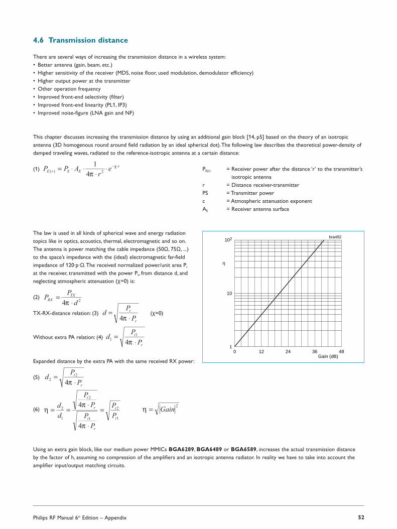
Philips RF Manual 6th Edition – Appendix 52
4.6 Transmission distance
There are several ways of increasing the transmission distance in a wireless system:• Better antenna (gain, beam, etc.)• Higher sensitivity of the receiver (MDS, noise floor, used modulation, demodulator efficiency) • Higher output power at the transmitter• Other operation frequency• Improved front-end selectivity (filter)• Improved front-end linearity (PL1, IP3)• Improved noise-figure (LNA gain and NF)
This chapter discusses increasing the transmission distance by using an additional gain block [14, p5] based on the theory of an isotropicantenna (3D homogenous round around field radiation by an ideal spherical dot).The following law describes the theoretical power-density ofdamped traveling waves, radiated to the reference-isotropic antenna at a certain distance:
(1) PE(r) = Receiver power after the distance ‘r’ to the transmitter’sisotropic antenna
r = Distance receiver-transmitterPS = Transmitter powerc = Atmospheric attenuation exponentAE = Receiver antenna surface
The law is used in all kinds of spherical wave and energy radiationtopics like in optics, acoustics, thermal, electromagnetic and so on.The antenna is power matching the cable impedance (50Ω, 75Ω, ...)to the space’s impedance with the (ideal) electromagnetic far-fieldimpedance of 120·p·Ω.The received normalized power/unit area Pr
at the receiver, transmitted with the power Pt, from distance d, andneglecting atmospheric attenuation (χ=0) is:
(2)
TX-RX-distance relation: (3) (χ=0)
Without extra PA relation: (4)
Expanded distance by the extra PA with the same received RX power:
(5)
(6)
bra492
10
102
η
1
Gain (dB)0 483612 24
Using an extra gain block, like our medium power MMICs BGA6289, BGA6489 or BGA6589, increases the actual transmission distance by the factor of h, assuming no compression of the amplifiers and an isotropic antenna radiator. In reality we have to take into account theamplifier input/output matching circuits.

Philips RF Manual 6th Edition – Appendix 53
Frequency (MHz)0.1 10001001 10
bra493
40
80
120
Fam(dB above
KT0b)
0
Night
Day
Galactic
BusinessResidentialRural
Atmospheric
Quiet Rural
4.7 Example: transmission distance limited by frequency and receiver quality
A receiver with a sensitivity of 0.1µV for 20dB SNR (=S/N) uses an antenna with effective surface of 3 cm2, 10 MHz. Determine the necessarytransmitter power for 1000 km distance neglecting the effects of atmospheric ionization anomalies, atmospheric attenuation and free spacepropagation.
PTX=84mW≅ +19.2dBm (χ=0)
The propagation loss caused by isotropic radiation is ARX=PTX-PIN=[19.2dBm-(-127dBm)]≈146.2dB
The median noise figure is Fam≈50dB at 10MHz.The receiver has an IF bandwidth of 10KHz.This gives a bandwidth terminated receiverNyquist noise floor of:
PNRflor=-134dBmª39.8◊10-18WPmed= PNRflor+Fam=-134dBm+50dB=-84dBmª3.98◊10-12W
At the present receiver, the effective equivalent front-end input noisefloor is specified to be 20dB below 0.1µV:PNRE=-127dBm-20dB=-147dBmª2◊10-18W
The effective resulting receiver input noise power is:PFR=PNRE+Pmed≈Pmed≈-84dBm
Resulting SNR(med)=PIN-PFR=-127dBm-(-84dBm)=-43dBand without man-made median noise +7dB
Two ideas for SNR improvement: Decrease of the BW, increase of the transmit power. Selected case: Increase of the transmitter power inorder of maintenance a SNR=20dB above the resulting median noise floor at the receiver’s location:
PINc= PFR+SNR=-84dBm+20dB=-64dBmPTXc=PINc+ARX=-64dBm+146.2dBm=+82.2dBmPTXc=166KW for a 10KHz bandwidths and SNR=20dB (Music)PTXc=166W for 100Hz bandwidth, SNR=10dB (e.g. Morse Code)
Conclusion:In shortwave (SW) bands, the necessary transmitter power is determined by the high amount of man-made noise. Due to that, the receiver’snoise figure in SW is not important. More important is the receiver’s input linearity (IP3) to handle the high-power man-made noise andintermodulation signals.Very important is the IF bandwidth and used modulation (min. bandwidth). Moving into the microwave range willdramatically reduce the man-made noise but the amount of galactic noise becomes the bottom-limiting factor.At such high frequencies,atmospheric absorption caused by water, oxygen and other gas molecules causes excessive rising of propagation losses. So a receiver’s noisefigure, gain and narrow bandwidth become increasingly important with rising frequency.
Philips RF Manual 6th Edition – Appendix 54
4.8 Filters in the receiver rail
The filters used and their primary responsibilities are:• A band-pass filter in front of the LNA, for image frequency band rejection• A band-pass filter after the LNA, for image noise suppression• A filter in the IF circuit, for selecting the RF transmission channel• A filter in the baseband, for selecting the baseband relevant frequency spectrum.
In spectrum analyzers and high-quality broadband short wave receivers, the first IF (Yig-Filters at SPA) is far above the received RF spectrum.Due to it, there is used a low pass filter preventing of front-end tuned tracking filters for image rejection purpose. Practically independent ofthe front-end pre-selection filter, the equivalent noise bandwidth is determined by the IF filter bandwidth.
4.9 Relationships and conversion of distortion parameters
oIP3≈oPL1dB+10.63dB in dBmiIP3≈oIP3-Gain in dBmiPL1dB≈oPL1dB-Gain in dBm
The offset factor of 10.63dB [1] can slightly vary. In other literature, 9.6dB is quoted. Ref. [1] is preferred, because of arithmetical detail explainingthe reason behind this value.
oIP3 = Output third order intercept point in dBmiIP3 = Input related third order intercept point in dBmoPL1 = Output 1dB gain compression point in dBmiPL1 = Input related 1dB gain compression point in dBmGain = Gain in dB
oIP3 typically used in transmitter systemsiIP3 typically used in receiver systems
References —Performance of cascaded RF blocks[1] Besser Associates, E. C. Niehenke, Ph.D.,Applied RF Techniques II, 2000[2] Thum/Wiesbeck/Kern, Hochfrequenzmeßtechnik,Verfahren und Meßsysteme,Tebner Stuttgart, 1997[3] Anritsu, Intermodulation (IMD) Measurements using 37300 Series Vector Network Analyzer, 11410-00257a.pdf[5] Keng Leong Fong,Thesis, Design and Optimization Techniques for Monolythic RF Downconversion Mixers, University of California,
Berkley, 1997, thesis.pdf[6] Halle Kivekäs, Dissertation, Design and characterization of downconversion mixers and the on-chip calibration techniques for
monolithic direct conversion radio receivers, Helsinki University of Technology, 2002, isbn9512261510.pdf[7] U.L.Rohde, J.Whitaker,T.T.N. Bucher, Communications Receievres, 2nd ed. Mc Graw Hill, 1996[9] Noise and Distortion in the RF Chain, Section 2.7, page 41, 41.pdf[10] Jin-Su Ko, High-Frequency Intermodulation Analysis of Cascode amplifiers, Media Team Samsung Electronics, Kyunggi-Do, Korea, 9-4.pdf[14] Philips Semiconductors, ‘2.4GHz Generic Front-End reference design’, 4th Edition Philips RF-Manual,Appendix A,A. Fix, March 2004[15] Bern University of Applied Since, Prof. F. Dellsperger, HTA-BE, Elektronik 2, Intermodulation, Dynamik, eq_IM.pdf

Philips RF Manual 6th Edition – Appendix 55
5. Introduction to GPS front-endsDue to the continuous size reductions and attractive pricing of semiconductor devices, GPS applications have become very popular in the pastfew years.A GPS navigation system is based on measuring and evaluating RF signals transmitted by GPS satellites.At least 24 active satellitesare necessary, at a distance of 20200 km above the Earth’s surface.All satellites transmit their civilian-use L1 signal simultaneously, down tousers at 1575.42 MHz in the so-called microwave L-band. Each satellite has its own C/A (Coarse Acquisition) code.
bra494
BASEBANDIC
RF-ICFRONT-END
INTERFACE
EARTH
IONOSPHAERE
Discrete genericfront-end
Antenna
GPSApplication
Satellite #1
Satellite #2
Satellite #....n
The U.S. navigation system, GPS, was originally started by the U.S. military in 1979. It will be updated to supply the L2 & L5 carriers for increa-sed performance in civil applications, while still providing the standard L1 RF carrier. GPS uses BPSK modulation on the L1 carrier and, begin-ning with launch of the modernized Block IIR, also on the L2 carrier.The L5 signal that will appear with the Block IIF satellites in 2006, will useQPSK modulation (Quadrature Phase Shift Keying).
Performance overview of current and up-coming GPS systems:
This satellite identifier C/A code is Pseudo Random and appears likeNoise in the frequency spectrum (=PRN C/A code).The L1 carrieris BPSK (Binary Phase Shift Keying) modulated by the C/A datacode, by the navigation data message and the encrypted P(Y)-code.Due to C/A’s PRN modulation, the carrier is DSSS modulated(Direct Sequence Spread Spectrum modulation).This DSSS spreadsthe former bandwidth signal to a satellite internal limited width of30 MHz.A GPS receiver must know the C/A code of each satellitefor selecting it out of the antenna’s RF spectrum. Because a satelliteis selected using an identification code, GPS is a CDMA system(Code Division Multiple Access).This RF signal is transmitted withenough power to ensure a minimum signal power level of -160 dBWon the Earth's surface.The absolute minimum receiver bandwidth is > 2 MHz.
The L1 carrier based GPS system uses:CDMA - DSSS - BPSK modulation
Need of a Topic Used Codes second reference Resolution Comments
base station
Today: basic Before May 2000:
positioning C/A Code on L1 No 25-100m Today - - -6-10m (resolution controlled by US)
Tomorrow: C/A Code on L1 Eliminates need for
basic positioning L2C Code on L2 No 1-5m costly DGPS in manyNew Code on L5 non-safety applications.
Today: advance L1 Code and Carrier max. distance to
positioning L2 Carrier Yes 2cm reference 10kmData Link
Tomorrow: L1 Code and Carrier max. distance to
advanced positioning L2 Code and Carrier Yes 2cm reference 100km;L5 Code and Carrier faster recovery following
Data Link signal interruption
Available GPS carrier frequenciesL1 Link 1 carrier frequency 1575.42 MHzL2 Link 2 carrier frequency 1227.6 MHzL3 Link 3 carrier frequency 1381.05 MHzL4 Link 4 carrier frequency 1379.913 MHzL5 Link 5 carrier frequency 1176.45 MHz

Philips RF Manual 6th Edition – Appendix 56
Competition in satellite-based navigation systems:In 2004, the European navigation system EGNOS was started. News forecasted the European system Galileo for 2008. GLONASS is a RussianNavigation System.
Comparison of the front-ends used in a GPS and in a GLONASS receiver:All GPS satellites use the same L1 frequency of 1575.42MHz, but different C/A codes, so a single front-end may be used.To achieve better skycoverage and accelerated operation, more than one antenna can be used. In this case, separate front-ends can be used. Using switches basedon Philips’ PIN-diodes makes it possible to select the antenna with the best signal in e.g. automotive applications, for operation in a city.
Each GLONASS satellite will use a different carrier frequency in the range of 1602.5625 MHz to 1615.5 MHz, with 562.5 kHz spacing, but allwith the same spread code.The normal method for receiving these signals uses several parallel working front-ends, perhaps with a commonfirst LNA and mixer, but certainly with different final local oscillators and IF mixers.
bra495
BASEBANDIC
RF - ICFRONT - END
INTERFACE
LOSS IN THE TRANSMISSIONMEDIUM
GLNA
Ax
Satellite #1...n
Ptx
PLNA
GANT
Pant = Ptx − AxPLNA = Pant + GantPrx = PLNA + GLNA
Pant
PRX
Satellite Generation Channe C/A Loop peek
II/IIA/IIR L1 -158.5dBW L2 -164.5dBW
IIR-M/IIF L1 -158.5dBWL2 -160.0dBW
The spread-spectrum modulated signal’s field strength is very weakand causes a negative SNR in the receiver input circuit — caused byNyquist noise determined by the analog front-end IF bandwidth:
Consumer
OEM Avionics
Survey /Mapping
Car Navigation
Military
Marine
Tracking /Machinecontrol
bra496
Application examples:• Personal Navigations• Railroads• Recreation, walking-tour• Off shore drilling• Satellite ops. ephemeris timing• Surveying & mapping• Network timing, synchronization• Fishing & boating• Arm clocks <Alarm clocks?>• Laptops and palms• Mobiles• Child safety• Car navigation systems• Fleet management systems• Telecom time reference • Highway toll systems• First-aid calls via mobiles
GPS Market & Applications

Philips RF Manual 6th Edition – Appendix 57
Simplified block diagram of a typical GPS receiver analog front-end IC
Typically, an integrated double-superhet receiver technology is used in the analog rail.The under sampling analog to digital converter (ADC) isintegrated in the analog front-end IC with a resolution of 1 to 2 bits. Due to under sampling, it acts as the third mixer for down-convertinginto to the digital stream IF band.After this ADC, comes the digital baseband processor. Up till this point, the SNR of the received satellitesignals is negative. In the baseband processor, the digital IF signal is parallel processed in several C/A correlators and NAV-data code discri-minators. During this processing, the effective Nyquest bandwidth is shrunk down to few Hertz. De-spreading and decoding of the GPS signalthen creates a positive SNR. Because typically, front-end ICs are produced in a highly integrated, low-power, relatively noisy semiconductortechnology, there is a need for an external Low-Noise-Amplifier (LNA) combined with band-pass filters. Because the available GPS IC chipsetson the market differ in their electrical performances like, gain, Noise Figure (NF), linearity and sensitivity, one and two-stage discrete front-endamplifiers are used.The numbers of filters in the front-end vary with the needs of the application’s target environment, costs and sizes.The processed number of GPS carriers, as well as the navigation accuracy, determines the min. allowed bandwidth of the analog front-end rail.
Philips Semiconductors offers MMICs with internal 50Ω matches at the input and output (I/O) and without internal matching.The internalmatched broadband MMICs typically need an output inductor for DC biasing and DC decoupling capacitors at the amplifier I/O.The internalnon-matched devices need an I/O matching network typically made by lumped LC circuits in an L-arrangement.This gives additional selectivity.Another advantage of this MMIC is the integrated temperature compensation in contrast to a transistor. In a system, typically the firstamplifier’s noise figure is very important. For example, the BGU2003 SiGe MMIC offers both (NF+IP3) with a good quality. Its silicon brotherBGA2003 comes with a lower IP3 and NF. IC chipsets that need high front-end gain made by one MMIC may be able to use the BGM1011or BGM1013.A two-stage design e.g. will use BGA2001, BGA2011 eventually combined with BGA2748 or BGA2715 or BGA2717.Some examples of configuration for an L1-carrier LNA are shown in the next two tables.
References:- Office of Space Commercialization, United States Department of Commerce- U.S. Coast Guard Navigation Center of Excellence- NAVSTAR Global Positioning System- NAVSTAR GPS USER EQUIPMENT INTRODUCTION- Royal school of Artillery, Basic science & technology section, BST, gunnery careers courses, the NAVSTAR Global Positioning System
bra497
RFamp BPrf MIX1 MIX2
RF(in)
BP1 IF1 BP2 A/Dconverter
Digital
IF2
LO2LO1 Sampler
AD
Single front-end amplifier:Amplifier BFG BFU BGU BGM BGM BFG BGA BGA BGA BGA BGA
325W 540 2003 1013 1011 410W 2011 2001 2003 2715 2748Gain 14dB 20dB 14dB 34dB 35dB 18dB 12dB 14dB 14dB 23.2dB 21dBNF 1dB 0.9dB 1.1dB 4.7dB 4.7dB 1.1dB 1.5dB 1.3dB 1.8dB 2.7dB 2dBIP3o(out) +24dBm +21dBm +21dBm +21dBm +20dBm +15dBm +10dBm +9.5dBm +9.2dBm +1dBm -1.6dBmMatching External External External Internal Internal External External External External Internal Internal
Two-stage cascaded circuit front-end amplifier:1st Stage BFG325W BFG410W BFG410W BFU540 BFG325W BGA2011 BGU2003 BGA2011 BGA2003 BGA20112nd Stage BFU540 BFU540 BGU2003 BFG410W BFG410W BGA2011 BGA2001 BGA2715 BGA2715 BGA2748Cascaded Gain 31dB 35dB 29dB 35dB 29dB 21dB 25dB 32.2dB 34dB 30dBCascaded NF 1.19dB 1.25dB 1.32dB 1.11dB 1.28dB 2dB 1.5dB 2.5dB 2.6dB 2.2dBCascaded IP3o +21dBm +21dBm +21dBm +15dBm +15dBm +10dBm +9.5dBm +1dBm +1dBm -1.6dBm
Note: [1] Gain=|S21|2; data @ 1.8GHz or the next one / approximated, found in the data sheet / diagrams[2] For cascaded amplifier equations refer to e.g. 4th edition RF Manual appendix, 2.4GHz Generic Front-End reference design[3] The evaluated cascaded amplifier includes an example interstage filter with 3dB insertion loss (NF=+3dB; IP3=+40dBm).[4] MMICs: BGAxxxx, BGMxxxx, BGUxxxx Transistors: BFGxxx, BFUxxx

Phil ips SemiconductorsPhilips Semiconductors is one of the world’s top semiconductor suppliers,with 20 manufacturing and assembly sites and a sales organization thatdelivers in 60 countries. For a complete up-to-date list of our sales officesplease visit our website http://www.semiconductors.philips.com/sales
All rights reserved. Reproduction in whole or in part is prohibited without the prior written consent of the copyright owner. The information presented in this document does not form part of anyquotation or contract, is believed to be accurate and reliable andmay be changed without notice. No liability will be accepted by the publisher for any consequence of its use. Publication thereof does notconvey nor imply any license under patent- or other industrial or intellectual property rights.
date of release: May 2005document order number: 9397 750 15125
Printed in the Netherlands
www.semiconductors.philips.com


