35
Semiconductors 5 th edition Product and design manual for RF Products October 2004 Appendix RF Manual

S e m i c o n d u c t o r s
5th editionProduct and design manual for RF Products
October 2004
Appendix RF Manual
Philips Semiconductors RF Manual 5th edition APPENDIX Product and design manual for RF Products
4322 252 06394 © Koninklijke Philips Elec tronics N.V.
RF Manual Appendix October 2004 2 of 35
Koninklijke Philips Electronics N.V. 2004 All rights reserved. Reproduction in whole or in part is prohibited without the prior written consent of the copyright owner. The information presented in this document does not form part of any quotation or contract, is believed to be accurate and reliable and may be changed without notice. No liability will be accepted by the publisher for any consequence of its use. Publication thereof does not convey nor imply any license under patent- or other industrial or intellectual property rights. Date of release: October 2004
Philips Semiconductors RF Manual 5th edition APPENDIX Product and design manual for RF Products
4322 252 06394 © Koninklijke Philips Elec tronics N.V.
RF Manual Appendix October 2004 3 of 35
Content appendix: Application notes:
Appendix A: BGA2715-17 general purpose
wideband amplifier, 50 Ohm Gain Blocks page: 4 - 8
Appendix B: BGA6x89 general purpose medium power amplifier, 50 Ohm Gain Blocks page: 9 -14
Appendix C: Introduction into the GPS Front-End page: 15 -18
Reference work: Appendix D: 2.4GHz Generic Front-End
reference design page: 19 - 25 Appendix E: RF Application-basics page: 26 - 29 Appendix F: RF Design-basics page: 30 - 34
Philips Semiconductors RF Manual 5th edition APPENDIX Product and design manual for RF Products
4322 252 06394 © Koninklijke Philips Elec tronics N.V.
RF Manual Appendix October 2004 4 of 35
Appendix A: BGA2715-17 general purpose wideband amplifiers, 50 Ohm Gain Blocks
APPLICATION INFORMATION BGA2715-17 Figure 2 shows a typical application circuit for the BGA2715-17 MMIC. The device is internally matched to 50 O, and therefore does not need any external matching. The value of the input and output DC blocking capacitors C2 and C3 should not be more than 100 pF for applications above 100 MHz. However, when the device is operated below 100 MHz, the capacitor value should be increased. The 22 nF supply decoupling capacitor C1 should be located as close as possible to the MMIC. The PCB top ground plane, connected to the pins 2, 4 and 5 must be as close as possible to the MMIC, preferably also below the MMIC. When using via holes, use multiple via holes, as close as possible to the MMIC. Application examples
RF output
Vs
RF input
GND2
RF in
Vs
RF out
C2 C3
C1
GND1
Philips Semiconductors RF Manual 5th edition APPENDIX Product and design manual for RF Products
4322 252 06394 © Koninklijke Philips Elec tronics N.V.
RF Manual Appendix October 2004 5 of 35
The MMIC is very suitable as IF amplifier in e.g. LNB's. The exellent wideband characteristics make it an easy building block.
As second amplifier after an LNA, the MMIC offers an easy matching, low noise solution.
to IF circuitor demodulatorfrom RF circuit
Mixer
Oscillator
widebandamplifier
to IF circuitor demodulator
antenna
Mixer
Oscillator
widebandamplifier
LNA
Philips Semiconductors RF Manual 5th edition APPENDIX Product and design manual for RF Products
4322 252 06394 © Koninklijke Philips Elec tronics N.V.
RF Manual Appendix October 2004 6 of 35
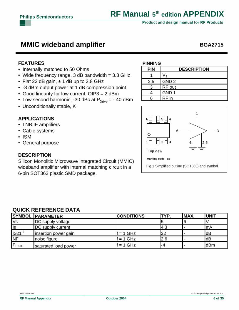
MMIC wideband amplifier BGA2715
FEATURES PINNING PIN
1 VS
2,5 GND 23 RF out4 GND 16 RF in
QUICK REFERENCE DATASYMBOL CONDITIONS TYP. MAX. UNITVs 5 6 VIs 4.3 - mA|S21|2 f = 1 GHz 22 - dBNF f = 1 GHz 2.6 - dBPL sat f = 1 GHz -4 - dBm
DESCRIPTION
noise figure
saturated load power
DC supply currentinsertion power gain
PARAMETERDC supply voltage
Fig.1 Simplified outline (SOT363) and symbol.
Top view
FEATURES • Internally matched to 50 Ohms• Wide frequency range, 3 dB bandwidth = 3.3 GHz• Flat 22 dB gain, ± 1 dB up to 2.8 GHz• -8 dBm output power at 1 dB compression point• Good linearity for low current, OIP3 = 2 dBm• Low second harmonic, -30 dBc at PDrive = - 40 dBm • Unconditionally stable, K APPLICATIONS• LNB IF amplifiers• Cable systems• ISM• General purpose
DESCRIPTIONSilicon Monolitic Microwave Integrated Circuit (MMIC)wideband amplifier with internal matching circuit in a6-pin SOT363 plastic SMD package.
Marking code: B6-
2,5
6
1
3
41 2 3
6 5 4
1 2 3
6 5 4
Philips Semiconductors RF Manual 5th edition APPENDIX Product and design manual for RF Products
4322 252 06394 © Koninklijke Philips Elec tronics N.V.
RF Manual Appendix October 2004 7 of 35
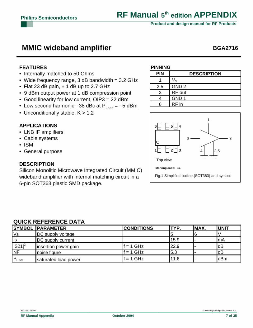
MMIC wideband amplifier BGA2716
FEATURES PINNING PIN
1 VS
2,5 GND 23 RF out4 GND 16 RF in
QUICK REFERENCE DATASYMBOL CONDITIONS TYP. MAX. UNITVs 5 6 VIs 15.9 - mA|S21|2 f = 1 GHz 22.9 - dBNF f = 1 GHz 5.3 - dBPL sat f = 1 GHz 11.6 - dBm
DESCRIPTION
noise figure
saturated load power
DC supply currentinsertion power gain
PARAMETERDC supply voltage
Fig.1 Simplified outline (SOT363) and symbol.
Top view
FEATURES • Internally matched to 50 Ohms• Wide frequency range, 3 dB bandwidth = 3.2 GHz• Flat 23 dB gain, ± 1 dB up to 2.7 GHz• 9 dBm output power at 1 dB compression point• Good linearity for low current, OIP3 = 22 dBm• Low second harmonic, -38 dBc at PLoad = - 5 dBm • Unconditionally stable, K > 1.2 APPLICATIONS• LNB IF amplifiers• Cable systems• ISM• General purpose
DESCRIPTIONSilicon Monolitic Microwave Integrated Circuit (MMIC)wideband amplifier with internal matching circuit in a6-pin SOT363 plastic SMD package.
Marking code: B7-
2,5
6
1
3
41 2 3
6 5 4
1 2 3
6 5 4
Philips Semiconductors RF Manual 5th edition APPENDIX Product and design manual for RF Products
4322 252 06394 © Koninklijke Philips Elec tronics N.V.
RF Manual Appendix October 2004 8 of 35
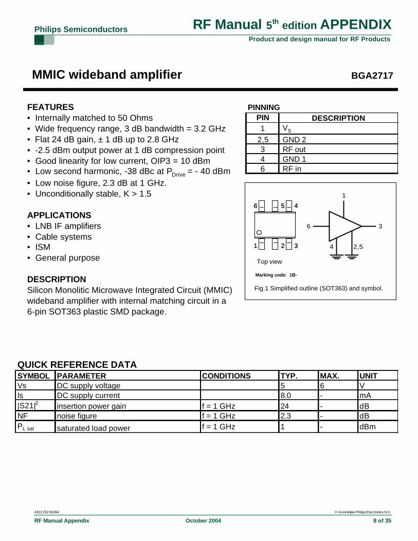
MMIC wideband amplifier BGA2717
FEATURES PINNING PIN
1 VS
2,5 GND 23 RF out4 GND 16 RF in
QUICK REFERENCE DATASYMBOL CONDITIONS TYP. MAX. UNITVs 5 6 VIs 8.0 - mA|S21|2 f = 1 GHz 24 - dBNF f = 1 GHz 2.3 - dBPL sat f = 1 GHz 1 - dBm
DESCRIPTION
noise figure
saturated load power
DC supply currentinsertion power gain
PARAMETERDC supply voltage
Fig.1 Simplified outline (SOT363) and symbol.
Top view
FEATURES • Internally matched to 50 Ohms• Wide frequency range, 3 dB bandwidth = 3.2 GHz• Flat 24 dB gain, ± 1 dB up to 2.8 GHz• -2.5 dBm output power at 1 dB compression point• Good linearity for low current, OIP3 = 10 dBm• Low second harmonic, -38 dBc at PDrive = - 40 dBm • Low noise figure, 2.3 dB at 1 GHz.• Unconditionally stable, K > 1.5 APPLICATIONS• LNB IF amplifiers• Cable systems• ISM• General purpose
DESCRIPTIONSilicon Monolitic Microwave Integrated Circuit (MMIC)wideband amplifier with internal matching circuit in a6-pin SOT363 plastic SMD package.
Marking code: 1B-
2,5
6
1
3
41 2 3
6 5 4
1 2 3
6 5 4
Philips Semiconductors RF Manual 5th edition APPENDIX Product and design manual for RF Products
4322 252 06394 © Koninklijke Philips Elec tronics N.V.
RF Manual Appendix October 2004 9 of 35
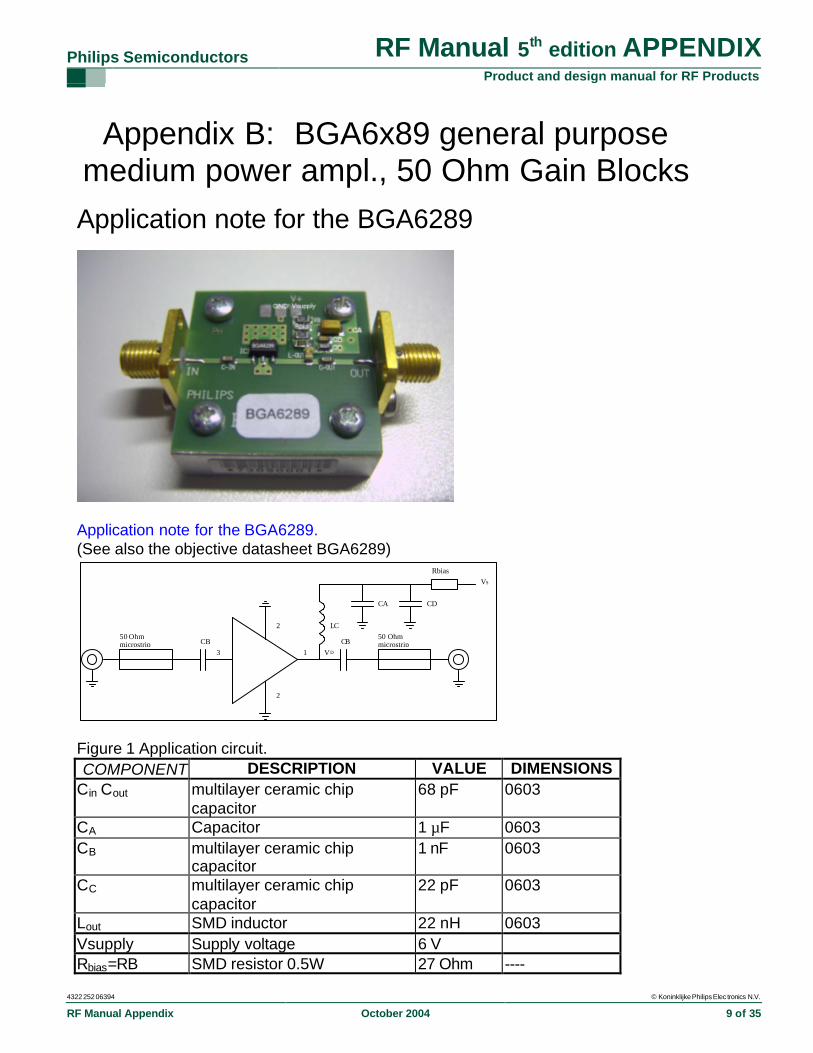
Appendix B: BGA6x89 general purpose medium power ampl., 50 Ohm Gain Blocks
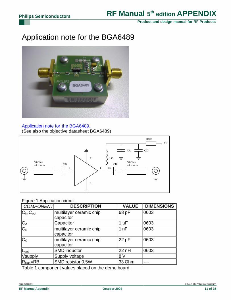
Application note for the BGA6289
Application note for the BGA6289. (See also the objective datasheet BGA6289)
Figure 1 Application circuit. COMPONENT DESCRIPTION VALUE DIMENSIONS
Cin Cout multilayer ceramic chip capacitor
68 pF 0603
CA Capacitor 1 µF 0603 CB multilayer ceramic chip
capacitor 1 nF 0603
CC multilayer ceramic chip capacitor
22 pF 0603
Lout SMD inductor 22 nH 0603 Vsupply Supply voltage 6 V Rbias=RB SMD resistor 0.5W 27 Ohm ----
VD
CB CB
CA CD
LC50 Ohmmicrostrip
50 Ohmmicrostrip
2
2
13
VS
Rbias
Philips Semiconductors RF Manual 5th edition APPENDIX Product and design manual for RF Products
4322 252 06394 © Koninklijke Philips Elec tronics N.V.
RF Manual Appendix October 2004 10 of 35
Table 1 component values placed on the demo board. CA is needed for optimal supply decoupling . Depending on frequency of operation the values of C in Cout and Lout can be changed (see table 2). COMPONENT Frequency (MHz)
500 800 1950 2400 3500 Cin Cout 220 pF 100 pF 68 pF 56 pF 39 pF CA 1 µF 1 µF 1 µF 1 µF 1 µF CB 1 nF 1 nF 1 nF 1 nF 1 nF CC 100 pF 68 pF 22 pF 22 pF 15 pF Lout 68 nH 33 nH 22 nH 18 nH 15 nH Table 2 component selection for different frequencies. Vsupply depends on Rbias used. Device voltage must be approximately 4 V (i.e. device current = 80mA). With formula 1 it is possible to operate the device under different supply voltages. If the temperature raises the device will draw more current, the voltage drop over Rbias will increase and the device voltage decrease, this mechanism provides DC stability. Measured small signal performance.
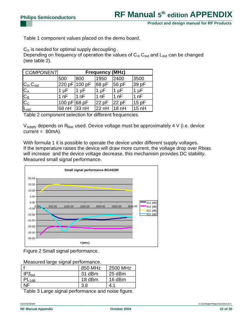
Figure 2 Small signal performance. Measured large signal performance. f 850 MHz 2500 MHz IP3out 31 dBm 25 dBm PL1dB 18 dBm 16 dBm NF 3.8 4.1 Table 3 Large signal performance and noise figure.
Small signal performance BGA6289
-30.00
-25.00
-20.00
-15.00
-10.00
-5.00
0.00
5.00
10.00
15.00
20.00
0.00 500.00 1000.00 1500.00 2000.00 2500.00 3000.00
f [MHz]
S11 [dB]S12 [dB]S21 [dB]S22 [dB]
Philips Semiconductors RF Manual 5th edition APPENDIX Product and design manual for RF Products
4322 252 06394 © Koninklijke Philips Elec tronics N.V.
RF Manual Appendix October 2004 11 of 35
Application note for the BGA6489
Application note for the BGA6489. (See also the objective datasheet BGA6489)
Figure 1 Application circuit. COMPONENT DESCRIPTION VALUE DIMENSIONS
Cin Cout multilayer ceramic chip capacitor
68 pF 0603
CA Capacitor 1 µF 0603 CB multilayer ceramic chip
capacitor 1 nF 0603
CC multilayer ceramic chip capacitor
22 pF 0603
Lout SMD inductor 22 nH 0603 Vsupply Supply voltage 8 V Rbias=RB SMD resistor 0.5W 33 Ohm ---- Table 1 component values placed on the demo board.
VD
CB CB
CA CD
LC50 Ohmmicrostrip
50 Ohmmicrostrip
2
2
13
VS
Rbias
Philips Semiconductors RF Manual 5th edition APPENDIX Product and design manual for RF Products
4322 252 06394 © Koninklijke Philips Elec tronics N.V.
RF Manual Appendix October 2004 12 of 35
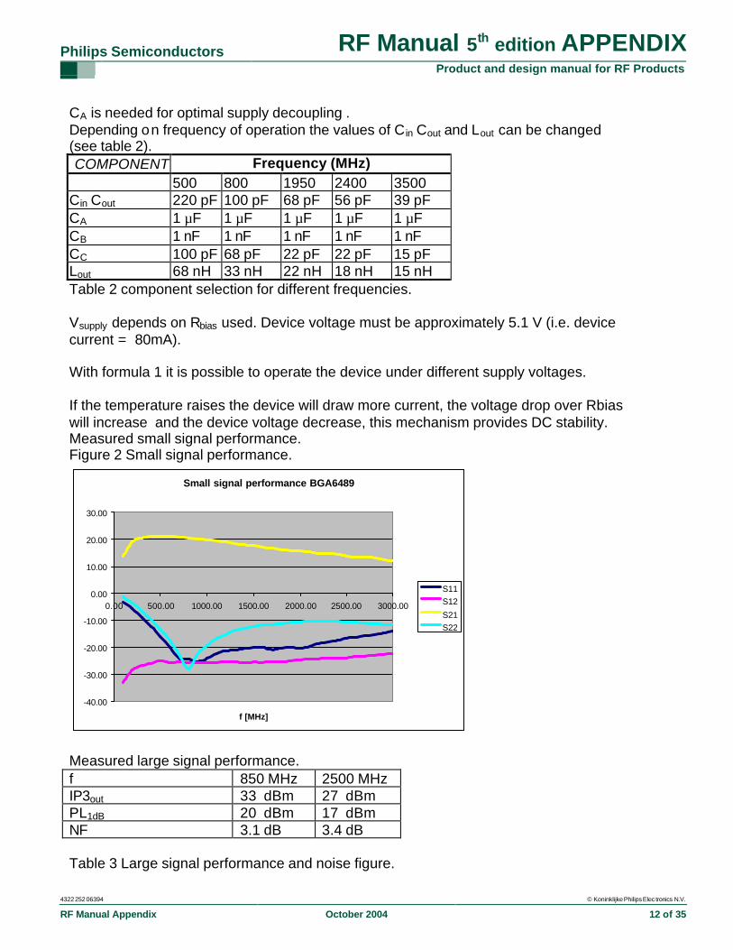
CA is needed for optimal supply decoupling . Depending on frequency of operation the values of C in Cout and Lout can be changed (see table 2). COMPONENT Frequency (MHz)
500 800 1950 2400 3500 Cin Cout 220 pF 100 pF 68 pF 56 pF 39 pF CA 1 µF 1 µF 1 µF 1 µF 1 µF CB 1 nF 1 nF 1 nF 1 nF 1 nF CC 100 pF 68 pF 22 pF 22 pF 15 pF Lout 68 nH 33 nH 22 nH 18 nH 15 nH Table 2 component selection for different frequencies. Vsupply depends on Rbias used. Device voltage must be approximately 5.1 V (i.e. device current = 80mA). With formula 1 it is possible to operate the device under different supply voltages. If the temperature raises the device will draw more current, the voltage drop over Rbias will increase and the device voltage decrease, this mechanism provides DC stability. Measured small signal performance. Figure 2 Small signal performance.
Measured large signal performance. f 850 MHz 2500 MHz IP3out 33 dBm 27 dBm PL1dB 20 dBm 17 dBm NF 3.1 dB 3.4 dB Table 3 Large signal performance and noise figure.
Small signal performance BGA6489
-40.00
-30.00
-20.00
-10.00
0.00
10.00
20.00
30.00
0.00 500.00 1000.00 1500.00 2000.00 2500.00 3000.00
f [MHz]
S11S12
S21S22
Philips Semiconductors RF Manual 5th edition APPENDIX Product and design manual for RF Products
4322 252 06394 © Koninklijke Philips Elec tronics N.V.
RF Manual Appendix October 2004 13 of 35
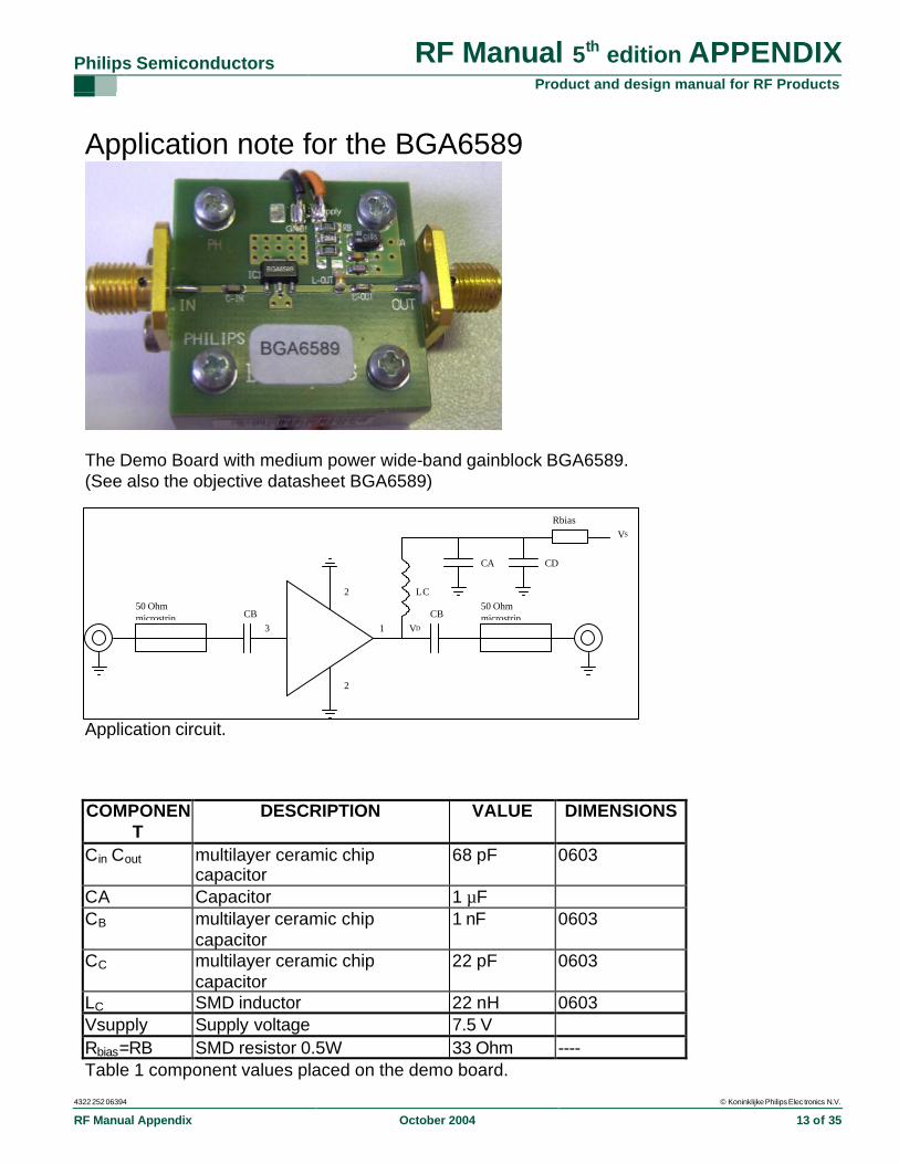
Application note for the BGA6589
The Demo Board with medium power wide-band gainblock BGA6589. (See also the objective datasheet BGA6589)
Application circuit. COMPONEN
T DESCRIPTION VALUE DIMENSIONS
Cin Cout multilayer ceramic chip capacitor
68 pF 0603
CA Capacitor 1 µF CB multilayer ceramic chip
capacitor 1 nF 0603
CC multilayer ceramic chip capacitor
22 pF 0603
LC SMD inductor 22 nH 0603 Vsupply Supply voltage 7.5 V Rbias=RB SMD resistor 0.5W 33 Ohm ---- Table 1 component values placed on the demo board.
VD
CB CB
CA CD
LC50 Ohmmicrostrip
50 Ohmmicrostrip
2
2
13
VS
Rbias
Philips Semiconductors RF Manual 5th edition APPENDIX Product and design manual for RF Products
4322 252 06394 © Koninklijke Philips Elec tronics N.V.
RF Manual Appendix October 2004 14 of 35
CA is needed for optimal supply decoupling . Depending on frequency of operation the values of C in Cout and Lout can be changed (see table 2). COMPONENT Frequency (MHz)
500 800 1950 2400 3500 Cin Cout 220 pF 100 pF 68 pF 56 pF 39 pF CA 1 µF 1 µF 1 µF 1 µF 1 µF CB 1 nF 1 nF 1 nF 1 nF 1 nF CC 100 pF 68 pF 22 pF 22 pF 15 pF Lout 68 nH 33 nH 22 nH 18 nH 15 nH Table 2 component selection for different frequencies. Vsupply depends on Rbias used. Device voltage must be approximately 4.8 V (i.e. device current = 83mA). With formula 1 it is possible to operate the device under different supply voltages. If the temperature raises the device will draw more current, the voltage drop over Rbias will increase and the device voltage decrease, this mechanism provides DC stability. Measured small signal performance.
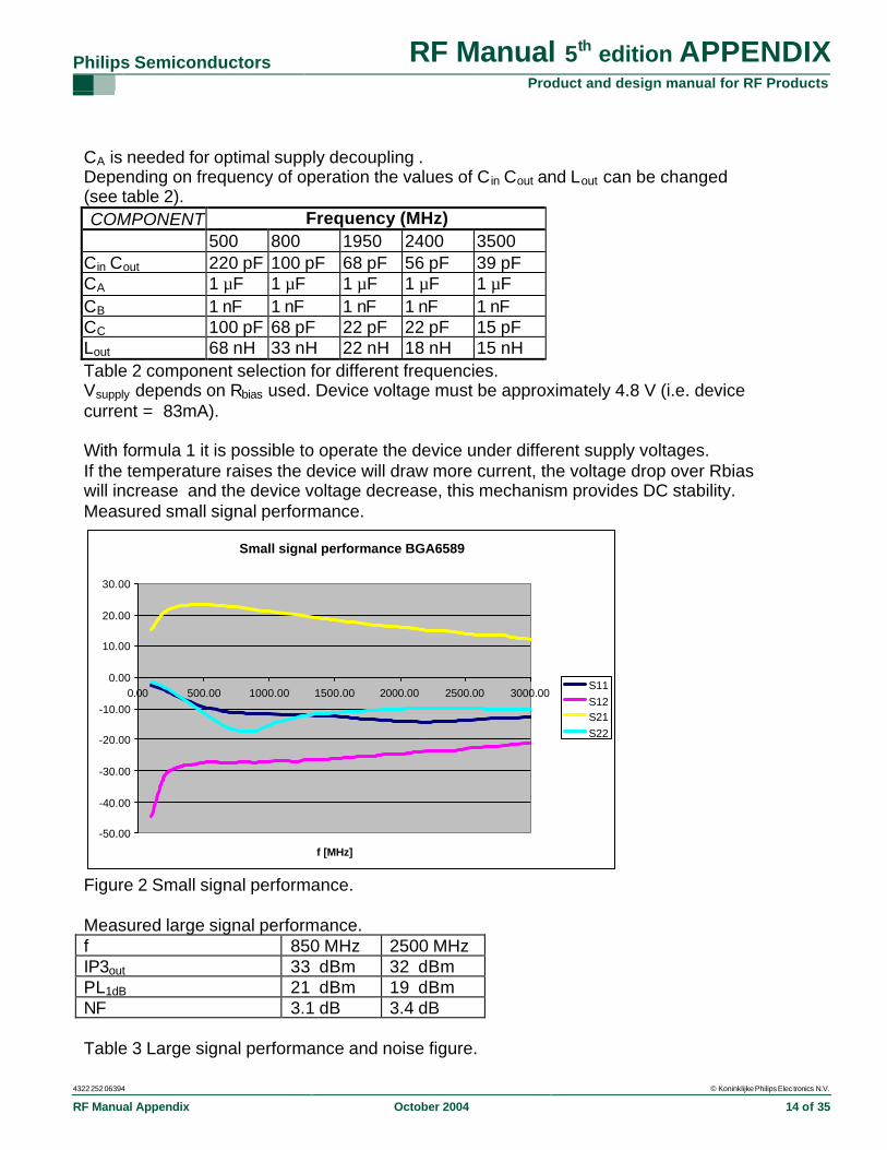
Figure 2 Small signal performance. Measured large signal performance. f 850 MHz 2500 MHz IP3out 33 dBm 32 dBm PL1dB 21 dBm 19 dBm NF 3.1 dB 3.4 dB Table 3 Large signal performance and noise figure.
Small signal performance BGA6589
-50.00
-40.00
-30.00
-20.00
-10.00
0.00
10.00
20.00
30.00
0.00 500.00 1000.00 1500.00 2000.00 2500.00 3000.00
f [MHz]
S11S12S21S22
Philips Semiconductors RF Manual 5th edition APPENDIX Product and design manual for RF Products
4322 252 06394 © Koninklijke Philips Elec tronics N.V.
RF Manual Appendix October 2004 15 of 35
Appendix C: Introduction GPS Front-End
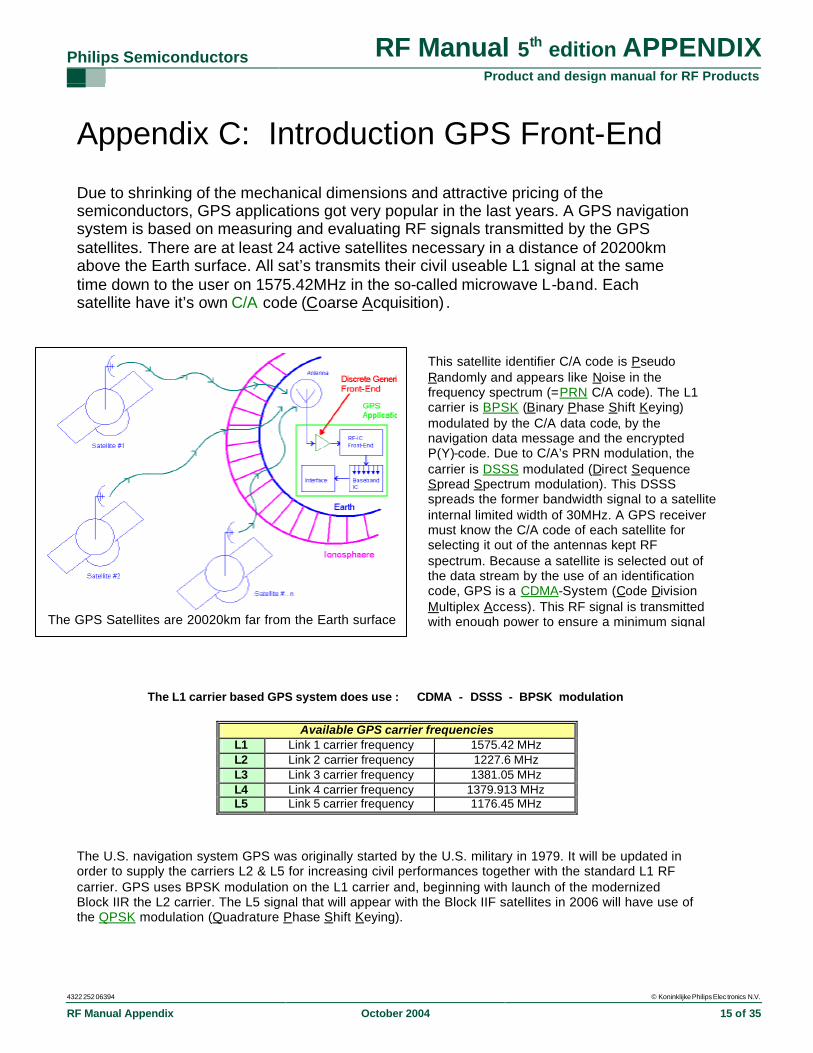
Due to shrinking of the mechanical dimensions and attractive pricing of the semiconductors, GPS applications got very popular in the last years. A GPS navigation system is based on measuring and evaluating RF signals transmitted by the GPS satellites. There are at least 24 active satellites necessary in a distance of 20200km above the Earth surface. All sat’s transmits their civil useable L1 signal at the same time down to the user on 1575.42MHz in the so-called microwave L-band. Each satellite have it’s own C/A code (Coarse Acquisition) .
The L1 carrier based GPS system does use : CDMA - DSSS - BPSK modulation
Available GPS carrier frequencies L1 Link 1 carrier frequency 1575.42 MHz L2 Link 2 carrier frequency 1227.6 MHz L3 Link 3 carrier frequency 1381.05 MHz L4 Link 4 carrier frequency 1379.913 MHz L5 Link 5 carrier frequency 1176.45 MHz
The U.S. navigation system GPS was originally started by the U.S. military in 1979. It will be updated in order to supply the carriers L2 & L5 for increasing civil performances together with the standard L1 RF carrier. GPS uses BPSK modulation on the L1 carrier and, beginning with launch of the modernized Block IIR the L2 carrier. The L5 signal that will appear with the Block IIF satellites in 2006 will have use of the QPSK modulation (Quadrature Phase Shift Keying).
The GPS Satellites are 20020km far from the Earth surface
This satellite identifier C/A code is Pseudo Randomly and appears like Noise in the frequency spectrum (=PRN C/A code). The L1 carrier is BPSK (Binary Phase Shift Keying) modulated by the C/A data code, by the navigation data message and the encrypted P(Y)-code. Due to C/A’s PRN modulation, the carrier is DSSS modulated (Direct Sequence Spread Spectrum modulation). This DSSS spreads the former bandwidth signal to a satellite internal limited width of 30MHz. A GPS receiver must know the C/A code of each satellite for selecting it out of the antennas kept RF spectrum. Because a satellite is selected out of the data stream by the use of an identification code, GPS is a CDMA-System (Code Division Multiplex Access). This RF signal is transmitted with enough power to ensure a minimum signal
Philips Semiconductors RF Manual 5th edition APPENDIX Product and design manual for RF Products
4322 252 06394 © Koninklijke Philips Elec tronics N.V.
RF Manual Appendix October 2004 16 of 35
The performances overview of the actual and the next up-coming GPS system:
Topic Used Codes
Need of a second
reference base station
Resolution Comments
Today basic positioning C/A Code on L1 No
Before May 2000: 25-100m Today 6-10m
(resolution controlled by US)
- - -
Tomorrow basic positioning
C/A Code on L1 L2C Code on L2 New Code on L5
No 1-5m
Eliminates need for costly DGPS in many
non-safety applications.
Today advance positioning
L1 Code and Carrier
L2 Carrier Data Link
Yes 2cm max. distance too reference 10km
Tomorrow advanced
positioning
L1 Code and Carrier
L2 Code and Carrier
L5 Code and Carrier
Data Link
Yes 2cm
max. distance too reference 100km;
faster recovery following signal
interruption
Competition Satellite based navigation systems: In 2004 will be start the European navigation system EGNOS. News forecasted the European system Galileo for 2008. GLONASS is a Russian Navigation System.
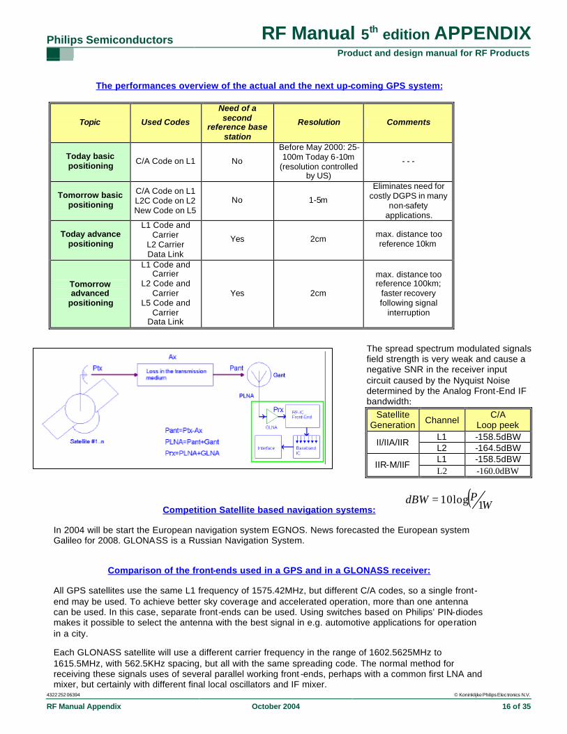
Comparison of the front-ends used in a GPS and in a GLONASS receiver: All GPS satellites use the same L1 frequency of 1575.42MHz, but different C/A codes, so a single front-end may be used. To achieve better sky coverage and accelerated operation, more than one antenna can be used. In this case, separate front-ends can be used. Using switches based on Philips’ PIN-diodes makes it possible to select the antenna with the best signal in e.g. automotive applications for operation in a city. Each GLONASS satellite will use a different carrier frequency in the range of 1602.5625MHz to 1615.5MHz, with 562.5KHz spacing, but all with the same spreading code. The normal method for receiving these signals uses of several parallel working front -ends, perhaps with a common first LNA and mixer, but certainly with different final local oscillators and IF mixer.
The spread spectrum modulated signals field strength is very weak and cause a negative SNR in the receiver input circuit caused by the Nyquist Noise determined by the Analog Front-End IF bandwidth:
Satellite Generation Channel
C/A Loop peek
L1 -158.5dBW II/IIA/IIR
L2 -164.5dBW L1 -158.5dBW
IIR-M/IIF L2 -160.0dBW
( )WPdBW 1log10=
Philips Semiconductors RF Manual 5th edition APPENDIX Product and design manual for RF Products
4322 252 06394 © Koninklijke Philips Elec tronics N.V.
RF Manual Appendix October 2004 17 of 35
GPS Marked & Applications
Marked of GPS Applications
Consumer
OEM Avionics
Survey / Mapping
Car Navigation
Military
Marine
Tracking / Machine Control
References: - Office of Space Commercialization, United States Department of Commerce - U.S. Coast Guard Navigation Center of Excellence - NAVSTAR Global Positioning System - NAVSTAR GPS USER EQUIPMENT INTRODUCTION - Royal school of Artillery, Basic science & technology section, BST, gunnery careers courses, the NAVSTAR Global Positioning System , …
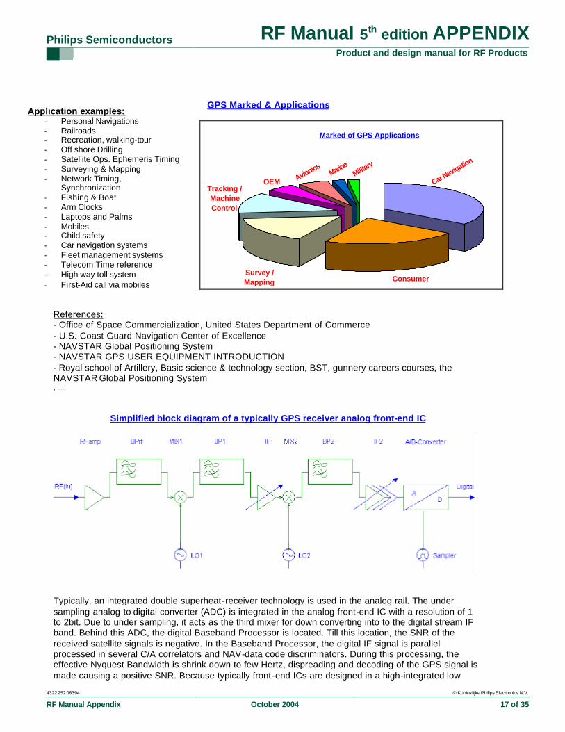
Simplified block diagram of a typically GPS receiver analog front-end IC
Typically, an integrated double superheat-receiver technology is used in the analog rail. The under sampling analog to digital converter (ADC) is integrated in the analog front-end IC with a resolution of 1 to 2bit. Due to under sampling, it acts as the third mixer for down converting into to the digital stream IF band. Behind this ADC, the digital Baseband Processor is located. Till this location, the SNR of the received satellite signals is negative. In the Baseband Processor, the digital IF signal is parallel processed in several C/A correlators and NAV-data code discriminators. During this processing, the effective Nyquest Bandwidth is shrink down to few Hertz, dispreading and decoding of the GPS signal is made causing a positive SNR. Because typically front-end ICs are designed in a high-integrated low
Application examples: - Personal Navigations - Railroads - Recreation, walking-tour - Off shore Drilling - Satellite Ops. Ephemeris Timing - Surveying & Mapping - Network Timing,
Synchronization - Fishing & Boat - Arm Clocks - Laptops and Palms - Mobiles - Child safety - Car navigation systems - Fleet management systems - Telecom Time reference - High way toll system - First-Aid call via mobiles
Philips Semiconductors RF Manual 5th edition APPENDIX Product and design manual for RF Products
4322 252 06394 © Koninklijke Philips Elec tronics N.V.
RF Manual Appendix October 2004 18 of 35
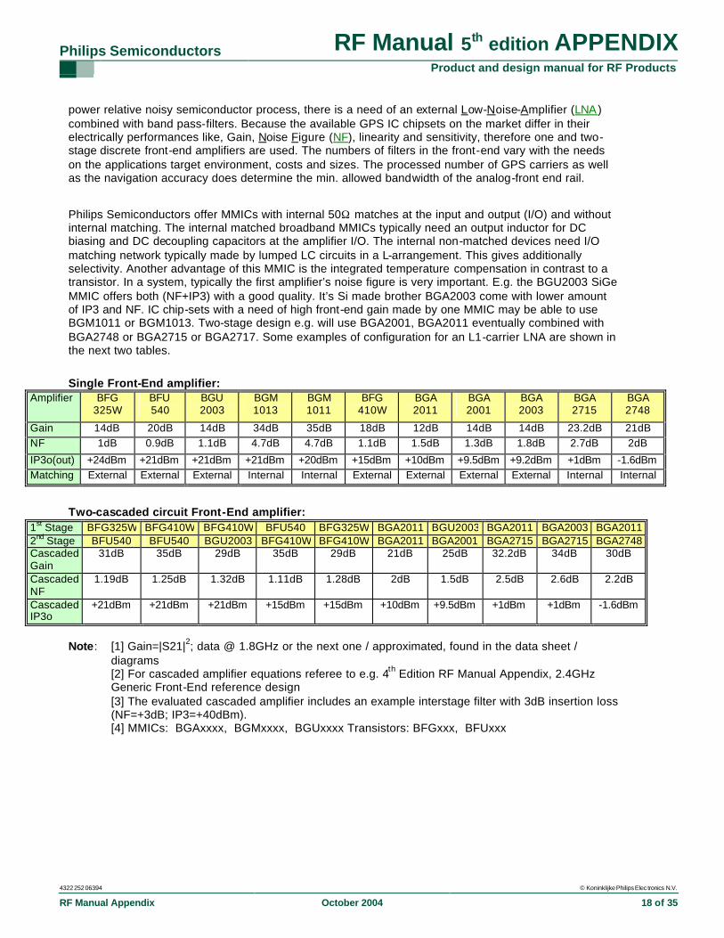
power relative noisy semiconductor process, there is a need of an external Low-Noise-Amplifier (LNA) combined with band pass-filters. Because the available GPS IC chipsets on the market differ in their electrically performances like, Gain, Noise Figure (NF), linearity and sensitivity, therefore one and two-stage discrete front-end amplifiers are used. The numbers of filters in the front-end vary with the needs on the applications target environment, costs and sizes. The processed number of GPS carriers as well as the navigation accuracy does determine the min. allowed bandwidth of the analog-front end rail.
Philips Semiconductors offer MMICs with internal 50Ω matches at the input and output (I/O) and without internal matching. The internal matched broadband MMICs typically need an output inductor for DC biasing and DC decoupling capacitors at the amplifier I/O. The internal non-matched devices need I/O matching network typically made by lumped LC circuits in a L-arrangement. This gives additionally selectivity. Another advantage of this MMIC is the integrated temperature compensation in contrast to a transistor. In a system, typically the first amplifier’s noise figure is very important. E.g. the BGU2003 SiGe MMIC offers both (NF+IP3) with a good quality. It’s Si made brother BGA2003 come with lower amount of IP3 and NF. IC chip-sets with a need of high front-end gain made by one MMIC may be able to use BGM1011 or BGM1013. Two-stage design e.g. will use BGA2001, BGA2011 eventually combined with BGA2748 or BGA2715 or BGA2717. Some examples of configuration for an L1-carrier LNA are shown in the next two tables.
Single Front-End amplifier:
Amplifier BFG 325W
BFU 540
BGU 2003
BGM 1013
BGM 1011
BFG 410W
BGA 2011
BGA 2001
BGA 2003
BGA 2715
BGA 2748
Gain 14dB 20dB 14dB 34dB 35dB 18dB 12dB 14dB 14dB 23.2dB 21dB NF 1dB 0.9dB 1.1dB 4.7dB 4.7dB 1.1dB 1.5dB 1.3dB 1.8dB 2.7dB 2dB
IP3o(out) +24dBm +21dBm +21dBm +21dBm +20dBm +15dBm +10dBm +9.5dBm +9.2dBm +1dBm -1.6dBm Matching External External External Internal Internal External External External External Internal Internal
Two-cascaded circuit Front-End amplifier:
1st Stage BFG325W BFG410W BFG410W BFU540 BFG325W BGA2011 BGU2003 BGA2011 BGA2003 BGA2011 2nd Stage BFU540 BFU540 BGU2003 BFG410W BFG410W BGA2011 BGA2001 BGA2715 BGA2715 BGA2748 Cascaded Gain
31dB 35dB 29dB 35dB 29dB 21dB 25dB 32.2dB 34dB 30dB
Cascaded NF
1.19dB 1.25dB 1.32dB 1.11dB 1.28dB 2dB 1.5dB 2.5dB 2.6dB 2.2dB
Cascaded IP3o
+21dBm +21dBm +21dBm +15dBm +15dBm +10dBm +9.5dBm +1dBm +1dBm -1.6dBm
Note: [1] Gain=|S21|2; data @ 1.8GHz or the next one / approximated, found in the data sheet /
diagrams [2] For cascaded amplifier equations referee to e.g. 4th Edition RF Manual Appendix, 2.4GHz Generic Front-End reference design [3] The evaluated cascaded amplifier includes an example interstage filter with 3dB insertion loss (NF=+3dB; IP3=+40dBm).
[4] MMICs: BGAxxxx, BGMxxxx, BGUxxxx Transistors: BFGxxx, BFUxxx
Philips Semiconductors RF Manual 5th edition APPENDIX Product and design manual for RF Products
4322 252 06394 © Koninklijke Philips Elec tronics N.V.
RF Manual Appendix October 2004 19 of 35
Appendix D: 2.4GHz Generic Front-End Reference design
Complete design description in previous RF Manual (4th edition),
including datasheet. Downloadable via RF Manual website: http://www.philips.semiconductors.com/markets/mms/products/discretes/documentation/rf_manual
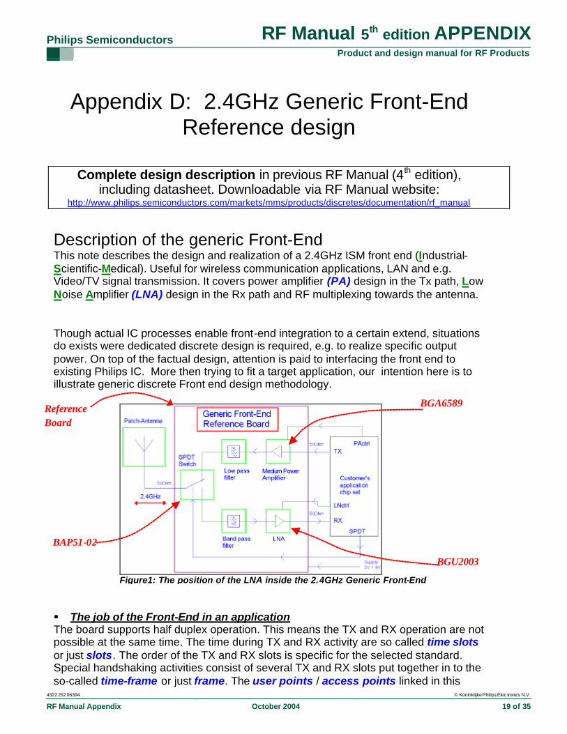
Description of the generic Front-End This note describes the design and realization of a 2.4GHz ISM front end (Industrial-Scientific-Medical). Useful for wireless communication applications, LAN and e.g. Video/TV signal transmission. It covers power amplifier (PA) design in the Tx path, Low Noise Amplifier (LNA) design in the Rx path and RF multiplexing towards the antenna. Though actual IC processes enable front-end integration to a certain extend, situations do exists were dedicated discrete design is required, e.g. to realize specific output power. On top of the factual design, attention is paid to interfacing the front end to existing Philips IC. More then trying to fit a target application, our intention here is to illustrate generic discrete Front end design methodology.
§ The job of the Front-End in an application The board supports half duplex operation. This means the TX and RX operation are not possible at the same time. The time during TX and RX activity are so called time slots or just slots. The order of the TX and RX slots is specific for the selected standard. Special handshaking activities consist of several TX and RX slots put together in to the so-called time-frame or just frame. The user points / access points linked in this
Figure1: The position of the LNA inside the 2.4GHz Generic Front-End
BAP51-02
BGU2003
BGA6589 Reference Board
Philips Semiconductors RF Manual 5th edition APPENDIX Product and design manual for RF Products
4322 252 06394 © Koninklijke Philips Elec tronics N.V.
RF Manual Appendix October 2004 20 of 35
wireless application must follow the same functionality of slots, same order of frames and timing procedure (synchronization). These kind of issues must be under the control of specific rules (standard) normally defined by Institutes or Organization like ETSI, IEEE, NIST, FCC, CEPT, and so on.
Applications for the Reference Board Some application ideas for the use of the Generic Front-End Reference Board § 2.4GHz WLAN § Wireless video, TV and remote control signal transmission § PC to PC data connection § PC headsets § PC wireless mouse, key board, and printer § Palm to PC, Keyboard, Printer connectivity § Supervision TV camera signal transmission § Wireless loudspeakers § Robotics § Short range underground walky-talky § Short range snow and stone avalanche person detector § Key less entry § Identification § Tire pressure systems § Garage door opener § Remote control for alarm-systems § Intelligent kitchen (cooking place, Microwave cooker and washing machine operator reminder) § Bluetooth § DSSS 2.4GHz WLAN (IEEE802.11b) § OFDM § 2.4GHz WLAN (IEEE802.11g) § Access Points § PCMCIA § PC Cards § 2.4GHz Cordless telephones § Wireless pencil as an input for Palms and PCs § Wireless hand scanner for a Palm § Identification for starting the car engine § Wireless reading of gas counters § Wireless control of soft-drink /cigarette/snag - SB machine § Communication between bus/taxi and the stop lights § Panel for ware house stock counting § Printers § Mobiles § Wireless LCD Display § Remote control § Cordless Mouse § Automotive, Consumer, Communication Please note: The used MMICs and PIN diodes can be used in other frequency ranges e.g. 300MHz to 3GHz for applications like communication, networking and ISM too.
Philips Semiconductors RF Manual 5th edition APPENDIX Product and design manual for RF Products
4322 252 06394 © Koninklijke Philips Elec tronics N.V.
RF Manual Appendix October 2004 21 of 35
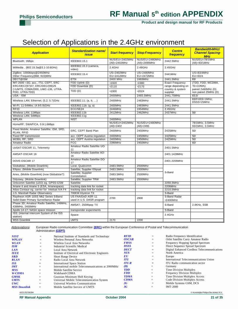
Selection of Applications in the 2.4GHz environment Application Standardization name/
issue Start frequency Stop Frequency Centre frequency
Bandwidth-MHz/ Channel Spacing-
MHz Bluetooth; 1Mbps IEEE802.15.1 NUS/EU=2402MHz
(All)=2402MHz NUS/EU=2480MHz (All)=2495MHz
2442.5MHz NUS/EU=78/1MHz (All)=93/1MHz
WiMedia , ([email protected]) IEEE802.15.3 (camera, video)
2.4GHz 2.49GHz 2.45GHz
ZigBee; 1000kbps@2450MHz Other Frequency(868; 915)MHz
IEEE802.15.4 US=2402MHz EU=2412MHz
US=2480MHz EU=2472MHz
2441MHz US=83/4MHz EU=60/4
DECT@ISM ETSI 2400 MHz 2483MHz 2441.5MHz 83/ FDD Uplink (D) ≈1920 ≈1980 FDD Downlink (D) ≈2110 ≈2170
IMT-2000 =3G; acc., ITU, CEPT, ERC ERC/DEC/(97)07; ERC/DEC/(99)25 (=UMTS, CDMA2000, UWC-136, UTRA-FDD, UTRA-TDD) TDD (D) ≈1900 ≈2024
Exact Frequency range depending on country & system supplier
(TDD, FDD; WCDMA, TD-CDMA); paired 2x60MHz (D) non paired 25MHz (D)
USA - ISM 2400MHz 2483.5MHz 2441.75MHz 83.5/
Wireless LAN; Ethernet; (5.2; 5.7)GHz IEEE802.11; (a, b, …) 2400MHz 2483MHz 2441.5MHz 83/FHSS=1MHz; DSSS=25MHz
Wi-Fi; 11-54Mbs; (4.9-5.9)GHz IEEE802.11b; (g, a) 2400MHz 2483MHz 2441.5MHz RFID ECC/SE24 2446MHz 2454MHz 2.45GHz Wireless LAN; 11Mbps IEEE802.11b 2412MHz 2462MHz 2437MHz 56/ Wireless LAN; 54Mbps IEEE802.11g WPLAN NIST 2400MHz
HomeRF; SWAP/CA, 0.8-1.6Mbps NUS/EU=2402MHz (All)=2402
NUS/EU=2480MHz (All)=2495
78/1MHz, 3.5MHz 93/1MHz, 3.5MHz
Fixed Mobile; Amateur Satellite; ISM, SRD, RLAN, RFID
ERC, CEPT Band Plan 2400MHz 2450MHz 2425MHz 50/
Fixed RF transmission acc. CEPT Austria regulation 2400MHz 2450MHz 2425MHz 50/ MOBIL RF; SRD acc. CEPT Austria regulation 2400MHz 2450MHz 2425MHz 50/ Amateur Radio FCC 2390MHz 2450MHz 60/
UoSAT-OSCAR 11, Telemetry Amateur Radio Satellite UO-11
2401.5MHz
AMSAT-OSCAR 16 Amateur Radio Satellite AO-16
2401.1428MHz
DOVE-OSCAR 17 Amateur Radio Satellite DO-17
2401.2205MHz
Globalstar, (Mobile Downlink) Loral, Qualcomm 2483.5MHz 2500MHz Ellipso, (Mobile Downlink) Satellite; Supplier Ellipsat 2483.5MHz 2500MHz
Aries, (Mobile Downlink) (now Globalstar?) Satellite; Supplier Constellation
2483.5MHz 2500MHz
Odyssey, (Mobile Downlink) Satellite; Supplier TRW 2483.5MHz 2500MHz
S-Band
Orbcomm Satellite (LEO) eg. GPSS-GSM Satellite 2250,5MHz Ariane 4 and Ariane 5 (ESA, Arianespace) tracking data link for rocket 2206MHz Atlas Centaur eg. carrier for Intelsat IVA F4 tracking data link for rocket 2210,5MHz J.S. Marshall Radar Observatory 700KW Klystron TX S-Band Raytheon ASR-10SS Mk2 Series S-Band Solid-State Primary Surveillance Radar
US FAA/DoD ASR-11 used in U.S. DASR program
2700 2900 S-Band Radar ≈2400MHz
Phase 3D; Amateur Radio Satellite; 146MHz, 436MHz, 2400MHz
AMSAT; 250Wpep TX S-Band 2.4KHz, SSB
Apollo 14-17; NASA space mission transponder experiments S-Band ISS; (internal Intercom System of the ISS station)
Space 2.4GHz
MSS Downlink UMTS 2170 2200
Abbreviations: European Radio communication Committee (ERC) within the European Conference of Postal and Telecommunication Administration (CEPT)
NIST = National Institute of Standards and Technology WPLAN = Wireless Personal Area Networks WLAN = Wireless Local Area Networks ISM = Industrial Scientific Medical LAN = Local Area Network IEEE = Institute of Electrical and Electronic Engineers SRD = Short Range Device RLAN = Radio Local Area Network ISS = International Space Station IMT = International mobile Telecommunications at 2000MHzMSS = Mobile Satellite Service W-CDMA = Wideband-CDMA GMSK = Gaussian Minimum Shift Keying UMTS = Universal Mobile Telecommunication System UWC = Universal Wireless Communication MSS Downlink = Mobile Satellite Service of UMTS
RFID = Radio Frequency Identification OSCAR = Orbit Satellite Carry Amateur Radio FHSS = Frequency Hopping Spread Spectrum DSSS = Direct Sequence Spread Spectrum DECT = Digital Enhanced Cordless Telecommunications NUS = North America EU = Europe ITU = International Telecommunications Union ITU-R = ITU Radio communication sector (D) = Germany TDD = Time Division Multiplex FDD = Frequency Division Multiplex TDMA = Time Division Multiplex Access CDMA = Code Division Multiplex Access 2G = Mobile Systems GSM, DCS 3G = IMT-2000
Philips Semiconductors RF Manual 5th edition APPENDIX Product and design manual for RF Products
4322 252 06394 © Koninklijke Philips Elec tronics N.V.
RF Manual Appendix October 2004 22 of 35
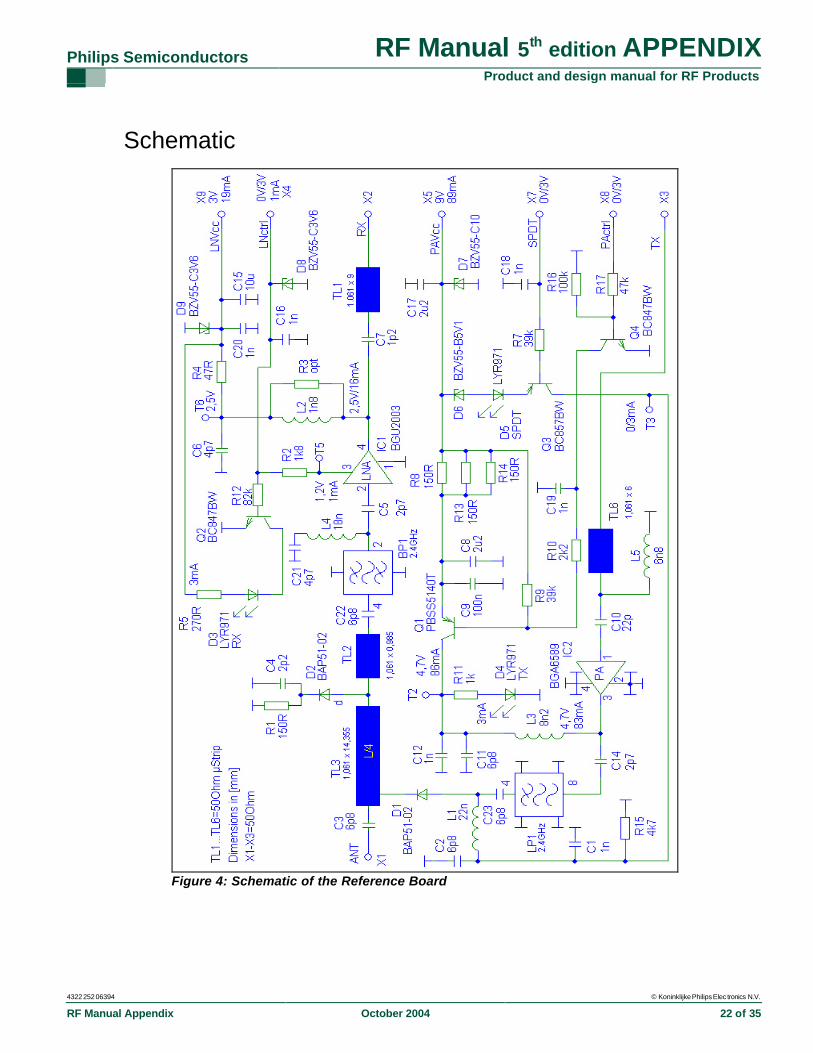
Schematic
Figure 4: Schematic of the Reference Board
Philips Semiconductors RF Manual 5th edition APPENDIX Product and design manual for RF Products
4322 252 06394 © Koninklijke Philips Elec tronics N.V.
RF Manual Appendix October 2004 23 of 35
Part List Part
Number Value Size Function / Short explanation Manufacturer Order Code Order
source IC1 BGU2003 SOT363 LNA-MMIC Philips Semiconductors BGU2003 PHL IC2 BGA6589 SOT89 TX-PA-MMIC Philips Semiconductors BGA6589 PHL Q1 PBSS5140T SOT23 TX PA-standby control Philips Semiconductors PBSS5140T PHL Q2 BC847BW SOT323 Drive of D3 Philips Semiconductors BC847BW PHL Q3 BC857BW SOT323 SPDT switching Philips Semiconductors BC857BW PHL Q4 BC847BW SOT323 PA logic level compatibility Philips Semiconductors BC847BW PHL D1 BAP51-02 SOD523 SPDT-TX; series part of the PIN diode switch Philips Semiconductors BAP51-02 PHL D2 BAP51-02 SOD523 SPDT-RX; shunt part of the PIN diode switch Philips Semiconductors BAP51-02 PHL D3 LYR971 0805 LED, yellow, RX and bias current control of IC1 OSRAM 67S5126 Bürklin D4 LYR971 0805 LED, yellow; TX OSRAM 67S5126 Bürklin D5 LYR971 0805 LED, yellow; SPDT; voltage level shifter OSRAM 67S5126 Bürklin D6 BZV55-B5V1 SOD80C Level shifting for being 3V/5V tolerant Philips Semiconductors BZV55-B5V1 PHL D7 BZV55-C10 SOD80C Board DC polarity & over voltage protection Philips Semiconductors BZV55-C10 PHL D8 BZV55-C3V6 SOD80C Board DC polarity & over voltage protection Philips Semiconductors BZV55-C3V6 PHL D9 BZV55-C3V6 SOD80C Board DC polarity & over voltage protection Philips Semiconductors BZV55-C3V6 PHL
R1 150Ω 0402 SPDT bias Yageo RC0402 Vitrohm512
26E558 Bürklin
R2 1k8 0402 LNA MMIC current CTRL Yageo RC0402 Vitrohm512
26E584 Bürklin
R3 optional 0402 L2 resonance damping; optional --- optional
R4 47Ω 0402 LNA MMIC collector bias Yageo RC0402 Vitrohm512
26E546 Bürklin
R5 270Ω 0402 RX LED current adj. Yageo RC0402 Vitrohm512
26E564 Bürklin
R7 39k 0402 Q3 bias SPDT Yageo RC0402 Vitrohm512
26E616 Bürklin
R8 150Ω 0805 PA-MMIC collector current adjust and temperature compensation
Yageo RC0805 Vitrohm503
11E156 Bürklin
R9 39k 0402 Helps switch off of Q1 Yageo RC0402 Vitrohm512
26E616 Bürklin
R10 2k2 0402 Q1 bias PActrl Yageo RC0402 Vitrohm512 26E586 Bürklin
R11 1kΩ 0402 LED current adjust; TX-PA Yageo RC0402 Vitrohm512
26E578 Bürklin
R12 82k 0402 Q2 drive Yageo RC0402 Vitrohm512 26E624 Bürklin
R13 150Ω 0805 PA-MMIC collector current adjust Yageo RC0805 Vitrohm503
11E156 Bürklin
R14 150Ω 0805 PA-MMIC collector current adjust Yageo RC0805 Vitrohm503 11E156 Bürklin
R15 4k7 0402 Improvement of SPDT-Off Yageo RC0402 Vitrohm512
26E594 Bürklin
R16 100k 0402 PActrl; logic level conversion Yageo RC0402 Vitrohm512 26E626 Bürklin
R17 47k 0402 PActrl; logic level conversion Yageo RC0402 Vitrohm512
26E618 Bürklin
L1 22nH 0402 SPDT RF blocking for biasing Würth Elektronik, WE-MK 744 784 22 WE L2 1n8 0402 LNA output matching Würth Elektronik, WE-MK 744 784 018 WE L3 8n2 0402 PAout Matching Würth Elektronik, WE-MK 744 784 082 WE L4 18nH 0402 LNA input match Würth Elektronik, WE-MK 744 784 18 WE L5 6n8 0402 PA input matching Würth Elektronik, WE-MK 744 784 068 WE C1 1nF 0402 medium RF short for SPDT bias Murata, X7R GRP155 R71H 102 KA01E Murata
C2 6p8 0402 medium RF short for SPDT bias Murata, C0G GRP1555 C1H 6R8 DZ01E
Murata
C3 6p8 0402 Antenna DC decoupling Murata, C0G GRP1555 C1H 6R8 DZ01E
Murata
C4 2p2 0402 RF short SPDT shunt PIN Murata, C0G GRP1555 C1H 2R2 CZ01E
Murata
C5 2p7 0402 DC decoupling LNA input + match Murata, C0G GRP1555 C1H 2R7 CZ01E
Murata
C6 4p7 0402 RF short output match Murata, C0G GRP1555 C1H 4R7 CZ01E Murata
C7 1p2 0402 LNA output matching Murata, C0G GRP1555 C1H 1R2 CZ0E Murata
C8 2u2/10V 0603 Removes the line ripple together with R8-R14 from PA supply rail
Murata, X5R GRM188 R61A 225 KE19D
Murata
C9 100nF/16V 0402 Ripple rejection PA Murata, Y5V GRM155 F51C 104 ZA01D Murata C10 22pF 0402 DC decoupling PA input Murata, C0G GRP1555 C1H 220 JZ01E Murata
C11 6p8 0402 RF short-bias PA Murata, C0G GRP1555 C1H 6R8 DZ01E Murata
C12 1nF 0402 PA, Supply RF short Murata, X7R GRP155 R71H 102 KA01E Murata
Philips Semiconductors RF Manual 5th edition APPENDIX Product and design manual for RF Products
4322 252 06394 © Koninklijke Philips Elec tronics N.V.
RF Manual Appendix October 2004 24 of 35
Part
Number Value Size Function / short explanation Manufacturer Order Code Order
source C14 2p7 0402 TX-PAout DC decoupling + matching Murata, C0G GRP1555 C1H 2R7
CZ01E Murata
C15 10u/6.3V 0805 dc rail LNVcc Murata, X5R GRM21 BR60J 106 KE19B Murata C16 1nF 0402 dc noise LNctrl Murata, X7R GRP155 R71H 102 KA01E Murata C17 2u2/10V 0603 PA dc rail Murata, X5R GRM188 R61A 225 KE34B Murata C18 1nF 0402 dc noise SPDT control Murata, X7R GRP155 R71H 102 KA01E Murata C19 1nF 0402 dc noise PActrl Murata, X7R GRP155 R71H 102 KA01E Murata C20 1nF 0402 dc noise LNVcc Murata, X7R GRP155 R71H 102 KA01E Murata
C21 4p7 0402 RF short for optional LNA input match Murata, C0G GRP1555 C1H 4R7 CZ01E
Murata
C22 6p8 0402 dc removal of RX-BP filter and matching Murata, C0G GRP1555 C1H 6R8 DZ01E
Murata
C23 6p8 0402 dc removal of TX-LP filter and matching Murata, C0G GRP1555 C1H 6R8 DZ01E Murata
BP1 fo=2.4GHz 1008 RX band pass input filtering Würth Elektronik 748 351 024 WE LP1 fc=2.4GHz 0805 TX low pass spurious filtering Würth Elektronik 748 125 024 WE
X1 SMA, female µStrip tab pin
12.7mm flange
1.3mm tab
Antenna connector, SMA, panel launcher, female, bulkhead receptacle with flange, PTFE, CuBe, CuNiAu
Telegärtner J01 151 A08 51 Telegärtner
X2 SMA, female µStrip tab pin
12.7mm flange
1.3mm tab
RX-Out connector, SMA, panel launcher, female, bulkhead receptacle with flange, PTFE, CuBe, CuNiAu
Telegärtner J01 151 A08 51 Telegärtner
X3 SMA, female µStrip tab pin
12.7mm flange
1.3mm tab
TX-IN connector, SMA, panel launcher, female, bulkhead receptacle with flange, PTFE, CuBe, CuNiAu
Telegärtner J01 151 A08 51 Telegärtner
X4 BÜLA30K green LNctrl, BÜLA30K, Multiple spring wire plugs, Solder terminal
Hirschmann 15F260 Bürklin
X5 BÜLA30K red PAVcc, BÜLA30K, Multiple spring wire plugs, Solder terminal Hirschmann 15F240 Bürklin
X6 BÜLA30K black GND, BÜLA30K, Multiple spring wire plugs, Solder terminal
Hirschmann 15F230 Bürklin
X7 BÜLA30K yellow SPDT, BÜLA30K, Multiple spring wire plugs, Solder terminal Hirschmann 15F250 Bürklin
X8 BÜLA30K blue PActrl, BÜLA30K, Multiple spring wire plugs, Solder terminal
Hirschmann 15F270 Bürklin
X9 BÜLA30K red LNVcc, BÜLA30K, Multiple spring wire plugs, Solder terminal Hirschmann 15F240 Bürklin
Y1 blue PActrl
40cm, 0.5qmm
Insulated stranded hook-up PVC wire, LiYv, blue, CuSn
VDE0812/9.72 92F566 Bürklin
Y2 red PAVcc
40cm, 0.5qmm,
Insulated stranded hook-up PVC wire, LiYv, red, CuSn
VDE0812/9.72 92F565 Bürklin
Y3 green LNctrl
40cm, 0.5qmm,
Insulated stranded hook-up PVC wire, LiYv, green, CuSn
VDE0812/9.72 92F567 Bürklin
Y4 black GND
40cm, 0.5qmm
Insulated stranded hook-up PVC wire, LiYv, black, CuSn
VDE0812/9.72 92F564 Bürklin
Y5 yellow SPDT
40cm, 0.5qmm,
Insulated stranded hook-up PVC wire, LiYv, yellow, CuSn
VDE0812/9.72 92F568 Bürklin
Y6 white LNVcc
40cm, 0.5qmm,
Insulated stranded hook-up PVC wire, LiYv, white, CuSn
VDE0812/9.72 92F569 Bürklin
Z1 - Z6 M2 M2 x 3mm Screw for PCB mounting Paul-Korth GmbH NIRO A2 DIN7985-H Paul-Korth
Z7 - Z12 M2,5 M2,5 x 4mm Screw for SMA launcher mounting Paul-Korth GmbH NIRO A2 DIN7985-H Paul-Korth
W1 FR4 compatible
47,5mm X 41,5mm
Epoxy 560µm; Cu=17.5µm; Ni=5µm; Au=0.3µm two layer double side
www.isola.de www.haefele-leiterplatten.de
DURAVER®-E-Cu, Qualität 104 MLB-DE 104
ML/2
Häfele Leiterplat -tentechnik
W2
Aluminum metal
finished yellow Aludine
47,5mm X 41,5mm X
10mm Base metal caring the pcb and SMA connectors --- --- ---
Philips Semiconductors RF Manual 5th edition APPENDIX Product and design manual for RF Products
4322 252 06394 © Koninklijke Philips Elec tronics N.V.
RF Manual Appendix October 2004 25 of 35
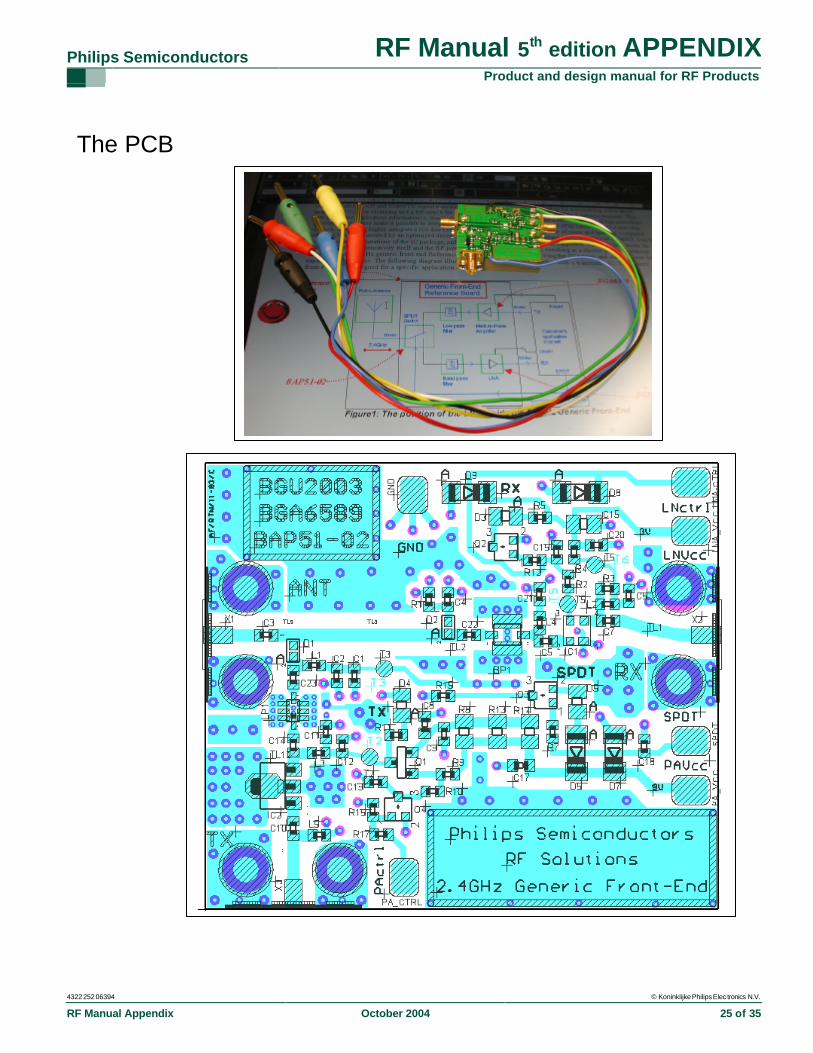
The PCB
Philips Semiconductors RF Manual 5th edition APPENDIX Product and design manual for RF Products
4322 252 06394 © Koninklijke Philips Elec tronics N.V.
RF Manual Appendix October 2004 26 of 35
Appendix E: RF Application-basics
Complete RF Application-basics in previous RF Manual (4th edition) which is downloadable via RF Manual website:
http://www.philips.semiconductors.com/markets/mms/products/discretes/documentation/rf_manual
1.1 Frequency spectrum 1.2 RF transmission system 1.3 RF Front-End For: Function of an antenna, examples of PCB design, Transistor Semiconductor Process, see RF Manual 4th edition on the RF Manual website.
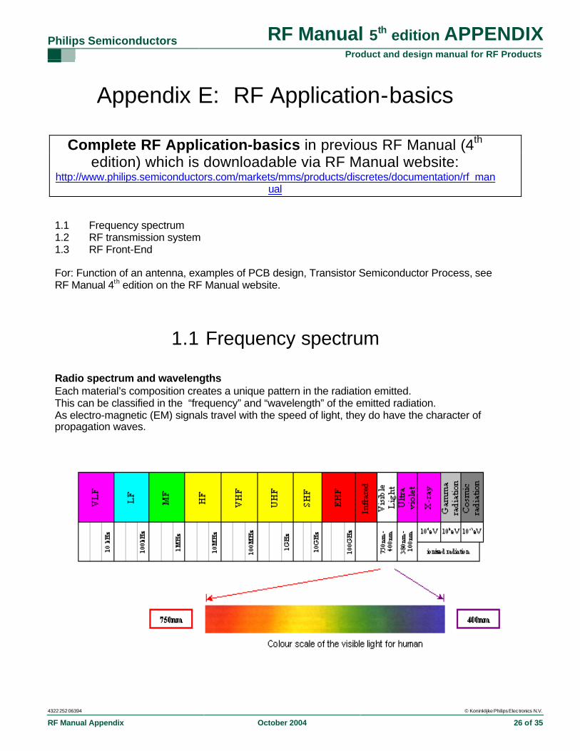
1.1 Frequency spectrum Radio spectrum and wavelengths Each material’s composition creates a unique pattern in the radiation emitted. This can be classified in the “frequency” and “wavelength” of the emitted radiation. As electro-magnetic (EM) signals travel with the speed of light, they do have the character of propagation waves.
Philips Semiconductors RF Manual 5th edition APPENDIX Product and design manual for RF Products
4322 252 06394 © Koninklijke Philips Elec tronics N.V.
RF Manual Appendix October 2004 27 of 35
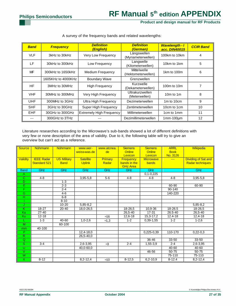
A survey of the frequency bands and related wavelengths:
Band Frequency Definition (English)
Definition (German)
Wavelength - λ acc. DIN40015
CCIR Band
VLF 3kHz to 30kHz Very Low Frequency Längswellen (Myriameterwellen) 100km to 10km 4
LF 30kHz to 300kHz Low Frequency Langwelle (Kilometerwellen) 10km to 1km 5
MF 300kHz to 1650kHz Medium Frequency Mittelwelle (Hektometerwellen) 1km to 100m 6
1605KHz to 4000KHz Boundary Wave Grenzwellen
HF 3MHz to 30MHz High Frequency Kurzwelle (Dekameterwellen) 100m to 10m 7
VHF 30MHz to 300MHz Very High Frequency Ultrakurzwellen (Meterwellen) 10m to 1m 8
UHF 300MHz to 3GHz Ultra High Frequency Dezimeterwellen 1m to 10cm 9
SHF 3GHz to 30GHz Super High Frequency Zentimeterwellen 10cm to 1cm 10
EHF 30GHz to 300GHz Extremely High Frequency Millimeterwellen 1cm to 1mm 11
--- 300GHz to 3THz --- Dezimillimeterwellen 1mm-100µm 12 Literature researches according to the Microwave’s sub-bands showed a lot of different definitions with very few or none description of the area of validity. Due to it, the following table will try to give an overview but can’t act as a reference.
Source Nührmann Nührmann www.wer-weiss-was.de
www.atcnea.de
Siemens Online
Lexicon
Siemens Online
Lexicon
ARRL Book
No. 3126
Wikipedia
Validity IEEE Radar Standard 521
US Military Band
Satellite Uplink
Primary Radar
Frequency bands in the GHz Area
Microwave bands
--- Dividing of Sat and Radar techniques
Band GHz GHz GHz GHz GHz GHz GHz A 0,1-0,225 C 4-8 3,95-5,8 5-6 4-8 4-8 4-8 3,95-5,8 D 1-3 E 2-3 60-90 60-90 F 2-4 90-140 G 4-6 140-220 H 6-8 I 8-10 J 10-20 5,85-8,2 5,85-8,2 K 18-27 20-40 18,0-26,5 18-26,5 10,9-36 18-26.5 18-26,5 Ka 27-40 26,5-40 17-31 26.5-40 26,5-40 Ku 12-18 ≈16 12,6-18 15,3-17,2 12.4-18 12,4-18 L 1-3 40-60 1,0-2,6 ≈1,3 1-2 0,39-1,55 1-2 1-2,6 M 60-100
mm 40-100 P 12,4-18,0 0,225-0,39 110-170 0,22-0,3 R 26,5-40,0 Q 36-46 33-50 33-50 S 3-4 2,6-3,95 ≈3 2-4 1,55-3,9 2-4 2,6-3,95 U 40,0-60,0 40-60 40-60 V 46-56 50-75 50-75 W 75-110 75-110 X 8-12 8,2-12,4 ≈10 8-12,5 6,2-10,9 8-12.4 8,2-12,4
Philips Semiconductors RF Manual 5th edition APPENDIX Product and design manual for RF Products
4322 252 06394 © Koninklijke Philips Electronics N.V.
RF Manual Appendix October 2004 28 of 35
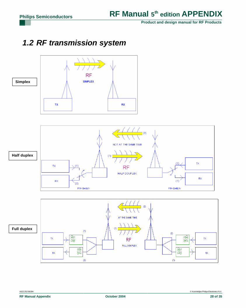
1.2 RF transmission system
Simplex
Half duplex
Full duplex
Philips Semiconductors RF Manual 5th edition APPENDIX Product and design manual for RF Products
4322 252 06394 © Koninklijke Philips Electronics N.V.
RF Manual Appendix October 2004 29 of 35
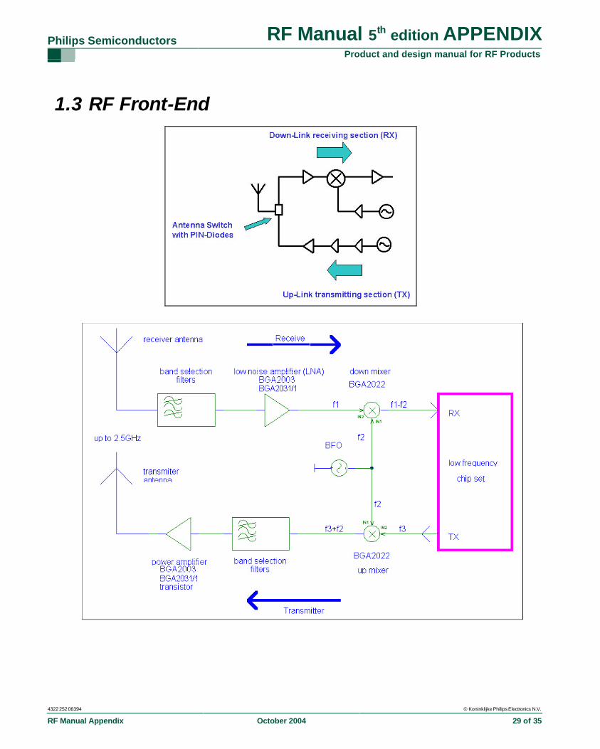
1.3 RF Front-End
Philips Semiconductors RF Manual 5th edition APPENDIX Product and design manual for RF Products
4322 252 06394 © Koninklijke Philips Electronics N.V.
RF Manual Appendix October 2004 30 of 35
Appendix F: RF Design-basics
Complete RF Design-basics in previous RF Manual (4th edition). RF Manual 4th edition downloadable via RF Manual website:
http://www.philips.semiconductors.com/markets/mms/products/discretes/documentation/rf_manual For: Fundamentals and RF Amplifier design Fundamentals, download RF Manual 4th edition on the RF Manual website.
Small signal RF amplifier parameters
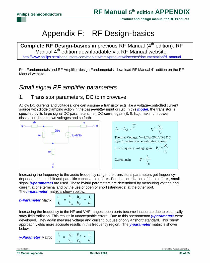
1. Transistor parameters, DC to microwave
At low DC currents and voltages, one can assume a transistor acts like a voltage-controlled current source with diode clamping action in the base-emitter input circuit. In this model, the transistor is specified by its large signal DC-parameters, i.e., DC-current gain (B, ß, hf e), maximum power dissipation, breakdown voltages and so forth.
Increasing the frequency to the audio frequency range, the transistor’s parameters get frequency-dependent phase shift and parasitic capacitance effects. For characterization of these effects, small signal h-parameters are used. These hybrid parameters are determined by measuring voltage and current at one terminal and by the use of open or short (standards) at the other port. The h-parameter matrix is shown below.
h-Parameter Matrix:
∗
=
2
1
2221
1211
2
1
ui
hhhh
iu
Increasing the frequency to the HF and VHF ranges, open ports become inaccurate due to electrically stray field radiation. This results in unacceptable errors. Due to this phenomenon y-parameters were developed. They again measure voltage and current, but use of only a “short” standard. This “short” approach yields more accurate results in this frequency region. The y-parameter matrix is shown below.
y-Parameter Matrix:
∗
=
2
1
2221
1211
2
1
uu
yyyy
ii
T
BE
VU
COC eII ⋅= E
Te I
Vr ='
Thermal Voltage: VT=kT/q≈26mV@25°C ICO=Collector reverse saturation current
Low frequency voltage gain: 'e
Cu r
RV ≈
Current gain B
C
II
ß =
Philips Semiconductors RF Manual 5th edition APPENDIX Product and design manual for RF Products
4322 252 06394 © Koninklijke Philips Electronics N.V.
RF Manual Appendix October 2004 31 of 35
Further increasing the frequency, the parasitic inductance of a “short” causes problem due to mechanical depending parasitic. Additionally, measuring voltage, current and it’s phase is quite tricky. The scattering parameters, or S-parameters, were developed based on the measurement of the forward and backward traveling waves to determine the reflection coefficients on a transistor’s terminals (or ports). The S-parameter matrix is shown below.
S-Parameter Matrix:
∗
=
2
1
2221
1211
2
1
aa
SSSS
bb
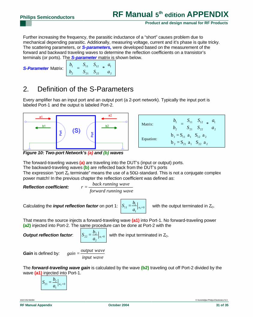
2. Definition of the S-Parameters Every amplifier has an input port and an output port (a 2-port network). Typically the input port is labeled Port-1 and the output is labeled Port-2.
Figure 10: Two-port Network’s (a) and (b) waves The forward-traveling waves (a) are traveling into the DUT’s (input or output) ports. The backward-traveling waves (b) are reflected back from the DUT’s ports The expression “port ZO terminate” means the use of a 50Ω-standard. This is not a conjugate complex power match! In the previous chapter the reflection coefficient was defined as:
Reflection coefficient: nning waveforward rung waveback runni
r =
Calculating the input reflection factor on port 1: 01
111 2== aa
bS with the output terminated in ZO.
That means the source injects a forward-traveling wave (a1) into Port-1. No forward-traveling power (a2) injected into Port-2. The same procedure can be done at Port-2 with the
Output reflection factor: 02
222 1== aa
bS with the input terminated in ZO.
Gain is defined by: waveinputwaveoutput
gain
=
The forward-traveling wave gain is calculated by the wave (b2) traveling out off Port-2 divided by the wave (a1) injected into Port-1.
01
221 2 == aa
bS
Matrix:
∗
=
2
1
2221
1211
2
1
aa
SSSS
bb
Equation: 2221212
2121111
aSaSbaSaSb⋅+⋅=⋅+⋅=
Philips Semiconductors RF Manual 5th edition APPENDIX Product and design manual for RF Products
4322 252 06394 © Koninklijke Philips Electronics N.V.
RF Manual Appendix October 2004 32 of 35
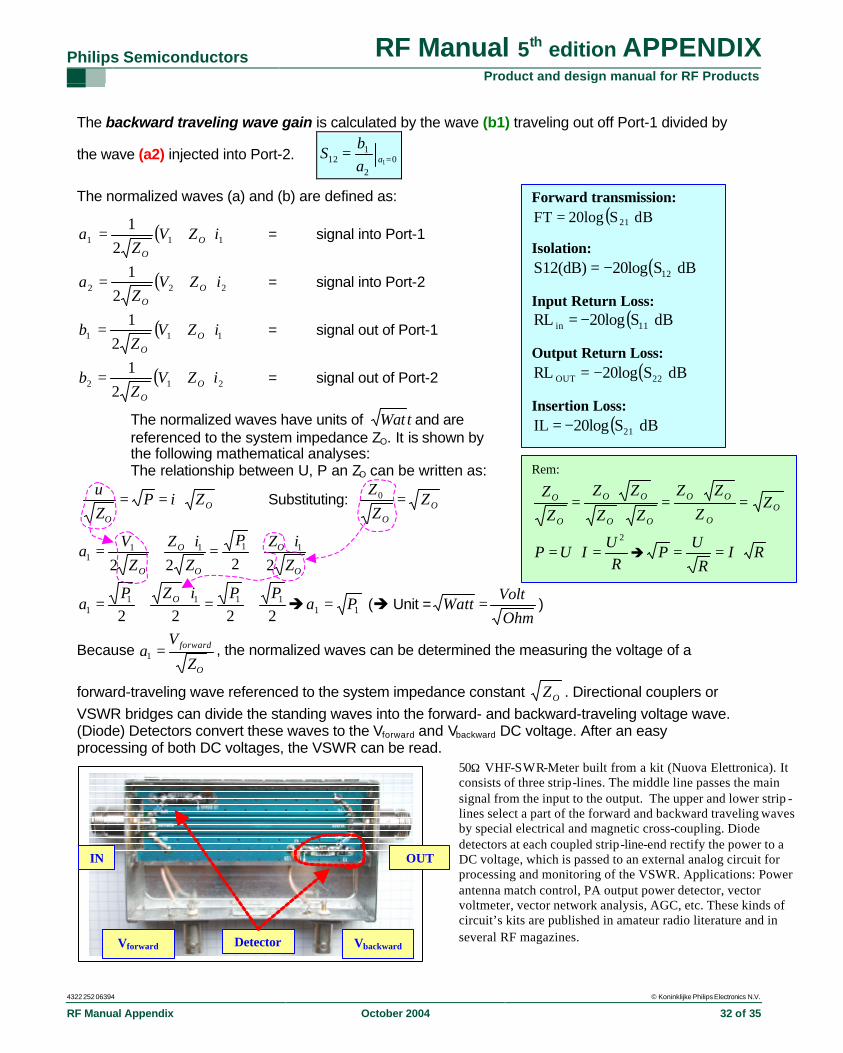
The backward traveling wave gain is calculated by the wave (b1) traveling out off Port-1 divided by
the wave (a2) injected into Port-2. 02
112 1== aa
bS
The normalized waves (a) and (b) are defined as:
( )1112
1iZV
Za O
O
⋅+= = signal into Port-1
( )2222
1iZV
Za O
O
⋅+= = signal into Port-2
( )1112
1iZV
Zb O
O
⋅+= = signal out of Port-1
( )2122
1iZV
Zb O
O
⋅+= = signal out of Port-2
The normalized waves have units of tWat and are referenced to the system impedance ZO. It is shown by the following mathematical analyses: The relationship between U, P an ZO can be written as:
OO
ZiPZu
⋅== Substituting: OO
ZZZ
=0
O
O
O
O
O ZiZP
ZiZ
ZV
a2222
11111
⋅+=
⋅+=
22221111
1
PPiZPa O +=
⋅+= è 11 Pa = (è Unit =
OhmVolt
Watt = )
Because O
forward
Z
Va =1 , the normalized waves can be determined the measuring the voltage of a
forward-traveling wave referenced to the system impedance constant OZ . Directional couplers or VSWR bridges can divide the standing waves into the forward- and backward-traveling voltage wave. (Diode) Detectors convert these waves to the Vforward and Vbackward DC voltage. After an easy processing of both DC voltages, the VSWR can be read.
Rem:
OO
OO
OO
OO
O
O ZZ
ZZ
ZZ
ZZ
ZZ
=⋅
=⋅
⋅=
RU
IUP2
=⋅= è RIR
UP ⋅==
50Ω VHF-SWR-Meter built from a kit (Nuova Elettronica). It consists of three strip-lines. The middle line passes the main signal from the input to the output. The upper and lower strip -lines select a part of the forward and backward traveling waves by special electrical and magnetic cross-coupling. Diode detectors at each coupled strip-line-end rectify the power to a DC voltage, which is passed to an external analog circuit for processing and monitoring of the VSWR. Applications: Power antenna match control, PA output power detector, vector voltmeter, vector network analysis, AGC, etc. These kinds of circuit’s kits are published in amateur radio literature and in several RF magazines.
IN OUT
Vforward Vbackward Detector
Forward transmission: ( )dBS20logFT 21=
Isolation:
( )dBS20logS12(dB) 12−=
Input Return Loss: ( )dBS20logRL 11in −=
Output Return Loss: ( )dBS20logRL 22OUT −=
Insertion Loss:
( )dBS20logIL 21−=
Philips Semiconductors RF Manual 5th edition APPENDIX Product and design manual for RF Products
4322 252 06394 © Koninklijke Philips Electronics N.V.
RF Manual Appendix October 2004 33 of 35
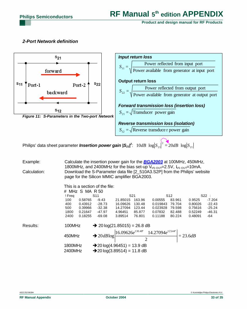
2-Port Network definition
Figure 11: S-Parameters in the Two-port Network
Philips’ data sheet parameter Insertion power gain |S21|2: 212
21 log20log10 SdBSdB ⋅=⋅ Example: Calculate the insertion power gain for the BGA2003 at 100MHz, 450MHz,
1800MHz, and 2400MHz for the bias set-up VVS-OUT=2.5V, IVS-OUT=10mA. Calculation: Download the S-Parameter data file [2_510A3.S2P] from the Philips’ website
page for the Silicon MMIC amplifier BGA2003.
This is a section of the file: # MHz S MA R 50 ! Freq S11 S21 S12 S22 : 100 0.58765 -9.43 21.85015 163.96 0.00555 83.961 0.9525 -7.204 400 0.43912 -28.73 16.09626 130.48 0.019843 79.704 0.80026 -22.43 500 0.39966 -32.38 14.27094 123.44 0.023928 79.598 0.75616 -25.24 1800 0.21647 -47.97 4.96451 85.877 0.07832 82.488 0.52249 -46.31 2400 0.18255 -69.08 3.89514 76.801 0.11188 80.224 0.48091 -64
Results: 100MHz è 20⋅log(21.85015) = 26.8 dB
450MHz è dBee
dB 6.232
27094.1409626.16log20
44.12348.130
=+ °°
1800MHz è20⋅log(4.96451) = 13.9 dB 2400MHz è20⋅log(3.89514) = 11.8 dB
Input return loss
portinput at generator from availablePower portinput from reflectedPower
11 =S
Output return loss
portoutput at generator from availablePower portoutput from reflectedPower
22 =S
Forward transmission loss (insertion loss)
gainpower Transducer21 =S Reverse transmission loss (isolation)
gainpower r transduceReverse12 =S
Philips Semiconductors RF Manual 5th edition APPENDIX Product and design manual for RF Products
4322 252 06394 © Koninklijke Philips Electronics N.V.
RF Manual Appendix October 2004 34 of 35
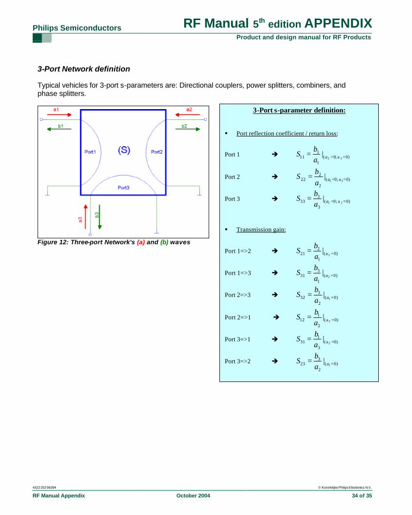
3-Port Network definition Typical vehicles for 3-port s-parameters are: Directional couplers, power splitters, combiners, and phase splitters.
Figure 12: Three-port Network's (a) and (b) waves
3-Port s-parameter definition: § Port reflection coefficient / return loss:
Port 1 è 0)a ;0(1
111 32
| === aab
S
Port 2 è 0)a ;0(2
222 31
| === aab
S
Port 3 è 0)a ;0(3
333 21
| === aab
S
§ Transmission gain:
Port 1=>2 è 0)a(1
221 3
| ==ab
S
Port 1=>3 è )0(1
331 2
| == aab
S
Port 2=>3 è )0(2
332 1
| == aab
S
Port 2=>1 è 0)a(2
112 3
| ==ab
S
Port 3=>1 è 0)a(3
131 2
| ==ab
S
Port 3=>2 è )0(2
323 1
| == aab
S
Philips Semiconductors RF Manual 5th edition APPENDIX Product and design manual for RF Products
4322 252 06394 © Koninklijke Philips Electronics N.V.
RF Manual Appendix October 2004 35 of 35
MAIN FILE RF Manual In separate file !
Download main RF Manual from internet:
http://www.philips.semiconductors.com/markets/mms/products/discretes/documentation/rf_manual
© Koninklijke Philips Electronics N.V. 2004
All rights are reserved. Reproduction in whole or in part is prohibited without the prior written consent of the copyright owner. The information presented in this document does not form part of any quotation or contract, is believed to be accurate and reliable and may be changed without notice. No liability will be accepted by the publisher for any consequence of its use. Publication thereof does not convey nor imply any license under patent- or other industrial or intellectual property rights.
Date of release: October 2004 Document order number: 4322 252 06394
Published in The Netherlands


