ams Datasheet Page 1 [v1-62] 2014-Nov-27 Document Feedback AS3930 Single Channel Low Frequency Wakeup Receiver The AS3930 is a single-channel low power ASK receiver that is able to generate a wake-up upon detection of a data signal which uses a LF carrier frequency between 110 - 150 kHz. The integrated correlator can be used for detection of a programmable 16-bit wake-up pattern. The AS3930 provides a digital RSSI value, it supports a programmable data rate. The AS3930 offers a real-time clock (RTC), which is either derived from a crystal oscillator or the internal RC oscillator. The programmable features of AS3930 enable to optimize its settings for achieving a longer distance while retaining a reliable wake-up generation. The sensitivity level of AS3930 can be adjusted in presence of a strong field or in noisy environments. The device is available in a 16-pin TSSOP and a 16-LD QFN (4x4) package. Ordering Information and Content Guide appear at end of datasheet. Key Benefits & Features The benefits and features of AS3930, Single Channel Low Frequency Wakeup Receiver are listed below: Figure 1: Added Value of Using AS3930 Benefits Features Enables low power active tags Single channel ASK wake-up receiver Selectable carrier frequency Carrier frequency range 110 – 150 kHz Highly resistant to false wake-ups 16-bit programmable wake-up pattern Improved immunity to false wake-ups Supporting doubling of wake-up pattern Allows frequency only detection Wake-up without pattern detection selectable Improved range with best-in-class sensitivity Wake-up sensitivity 100μVRMS (typ.) Adjustable range Sensitivity level adjustable Provides tracking of false wake-ups False wake-up counter Ensures wake-up in a noise environment Periodical forced wake-up supported (1s – 2h) Extended battery life Current consumption in listening mode 1.37 μA (typ.) Flexible clock configuration RTC based 32 kHz XTAL, RC-OSC, or external clock General Description
Transcript
AS3930Single Channel Low Frequency Wakeup Receiver
The AS3930 is a single-channel low power ASK receiver that is able to generate a wake-up upon detection of a data signal which uses a LF carrier frequency between 110 - 150 kHz. The integrated correlator can be used for detection of a programmable 16-bit wake-up pattern.
The AS3930 provides a digital RSSI value, it supports a programmable data rate. The AS3930 offers a real-time clock (RTC), which is either derived from a crystal oscillator or the internal RC oscillator.
The programmable features of AS3930 enable to optimize its settings for achieving a longer distance while retaining a reliable wake-up generation. The sensitivity level of AS3930 can be adjusted in presence of a strong field or in noisy environments. The device is available in a 16-pin TSSOP and a 16-LD QFN (4x4) package.
Ordering Information and Content Guide appear at end of datasheet.
Key Benefits & FeaturesThe benefits and features of AS3930, Single Channel Low Frequency Wakeup Receiver are listed below:
Figure 1:Added Value of Using AS3930
Benefits Features
Enables low power active tags Single channel ASK wake-up receiver
Selectable carrier frequency Carrier frequency range 110 – 150 kHz
Highly resistant to false wake-ups 16-bit programmable wake-up pattern
Improved immunity to false wake-ups Supporting doubling of wake-up pattern
Allows frequency only detection Wake-up without pattern detection selectable
Improved range with best-in-class sensitivity Wake-up sensitivity 100μVRMS (typ.)
Adjustable range Sensitivity level adjustable
Provides tracking of false wake-ups False wake-up counter
Ensures wake-up in a noise environment Periodical forced wake-up supported (1s – 2h)
Extended battery life Current consumption in listening mode 1.37 μA (typ.)
Flexible clock configuration RTC based 32 kHz XTAL, RC-OSC, or external clock
ApplicationsThe AS3930, Single Channel Low Frequency Wakeup Receiver is ideal for Active RFID tags, real-time location systems, operator identification, access control, and wireless sensors.
Figure 2:AS3930 Typical Application Diagram with Crystal Oscillator
Operates from a 3V battery Operating supply range 2.4V – 3.6V (TA = 25°C)
Industrial temperature range Operation temperature range -40°C to +85°C
Stresses beyond those listed in Absolute Maximum Ratings may cause permanent damage to the device. These are stress ratings only. Functional operation of the device at these or any other conditions beyond those indicated in Electrical Characteristics is not implied. Exposure to absolute maximum rating conditions for extended periods may affect device reliability.
Figure 9:Absolute Maximum Ratings
Parameter Min Max Unit Note
Electrical Parameters
DC supply voltage (VDD) -0.5 5 V
Input pin voltage (VIN) -0.5 5 V
Input current (latch up immunity) (ISOURCE) -100 100 mA Norm: Jedec 78
Electrostatic Discharge
Electrostatic discharge (ESD) ±2 kV Norm: MIL 883 E method 3015 (HBM)
Continuous Power Dissipation
Total power dissipation (all supplies and outputs)
(Pt) 0.07 mW
Temperature Ranges and Storage Conditions
Storage temperature (Tstrg) -65 150 °C
Package body temperature (Tbody) 260 °C
Norm: IPC/JEDEC J-STD-020 The reflow peak soldering temperature
(body temperature) is specified according IPC/JEDEC J-STD-020 “Moisture/Reflow
Sensitivity Classification for Non-hermetic Solid State Surface Mount Devices”.
Humidity non-condensing 5 85 %
Moisture Sensitivity Level (MSL) 3Represents a maximum floor life time of
The AS3930 is a one-dimensional low power low-frequency wake-up receiver. The AS3930 is capable of detecting the presence of an inductive coupled carrier and extract the envelope of the ON-OFF-Keying (OOK) modulated carrier. In case the carrier is Manchester coded, then the clock is recovered from the transmitted signal and the data can be correlated with a programmed pattern. If the detected pattern corresponds to the stored one, then a wake-up signal (IRQ) is risen up. The pattern correlation can be bypassed in which case the wake-up detection is based only on the frequency detection.
The AS3930 is made up of a single receiving channel, one envelop detector, one data correlator, 8 programmable registers with the main logic and a real time clock.
The digital logic can be accessed by an SDI. The real time clock can be based on a crystal or on an internal RC. If the internal RC oscillator is used, a calibration procedure can be performed to improve its accuracy.
Figure 16:Block Diagram of LF Wake-up Receiver AS3930
• 32.768 kHz crystal with its two pulling capacitors - XTAL and CL - (it is possible to omit these components if the internal RC oscillator is used instead of the crystal oscillator).
• Input LC resonator.
In case the internal RC-oscillator is used (no crystal oscillator is mounted), the pin XIN has to be connected to the supply, while pin XOUT should stay floating. Application diagrams with and without crystal are shown in Figure 2 and Figure 3.
Operating Modes
Power Down ModeIn Power Down Mode AS3930 is completely switched OFF. The typical current consumption is 400 nA.
Listening ModeIn listening mode only the channel amplifier and the RTC are running. In this mode the system detects the presence of a carrier. In case the carrier is detected, the RSSI can be displayed.
In this mode it is possible to distinguish the following three sub modes:
Standard Listening Mode
The channel amplifier that is capable of detecting the presence of the carrier frequency, is active all the time.
ON/OFF Mode (Low Power mode )
The channel amplifier is active for one millisecond after which it is switched OFF. The OFF-time is programmable (see R4<7:6>).
Further, for both sub modes, it is possible to enable a feature called Artificial Wake-up. If the Artificial Wake-up is enabled, then the AS3930 produces an interrupt after a certain time regardless of whether any activity is detected on the input. The period of the Artificial Wake-up is defined in the register R8<2:0>. The user can distinguish between Artificial Wake-up and Wake-up based on the field detection (frequency or pattern detection) since the Artificial Wake-up interrupt lasts only 128μs. With this interrupt the microcontroller (μC) can get feedback on the surrounding environment (e.g. read the false wake-up register R13<7:0>) and/or take actions in order to change the setup.
Preamble Detection / Pattern CorrelationThe preamble detection and pattern correlation are only considered for the wake-up when the data correlator function is enabled (see R1<1>). The correlator searches first for preamble frequency (constant frequency of Manchester clock defined according to bit-rate transmission, see Figure 36) and then for data pattern.
If the pattern is matched, then the wake-up interrupt is displayed on the WAKE output and the chip goes in data receiving mode. If the pattern fails, then the internal wake-up is terminated and no IRQ is produced.
Data ReceivingAfter a successful wake-up the chip enters the data receiving mode. In this mode the chip can be retained a normal OOK receiver. The received data are streamed out on the pin DAT. It is possible to put the chip back to listening mode either with a direct command (CLEAR_WAKE see Figure 24) or by using the timeout feature. This feature automatically sets the chip back to listening mode after a certain time R7<7:5>.
Serial Data Interface (SDI)This 4-wires interface is used by the Microcontroller (μC) to program the AS3930. The maximum clock frequency of the SDI is 2MHz.
Figure 20:Serial Data Interface (SDI) pins
Note(s): SDO is set to tristate if CS is low. In this way more than one device can communicate on the same SDO bus.
SDI Command Structure. To program the SDI the CS signal has to go high. A SDI command is made up by a two bytes serial command and the data is sampled on the falling edge of SCLK. Figure 21 shows how the command looks like, from the MSB (B15) to LSB (B0). The command stream has to be sent to the SDI from the MSB (B15) to the LSB (B0).
Figure 21:SDI Command Structure
The first two bits (B15 and B14) define the operating mode. There are three modes available (write, read, direct command) plus one spare (not used), as shown in Figure 22.
Figure 22:Bits B15, B14
Name Signal Signal Level Description
CS Digital Input with pull down CMOS Chip Select
SDI Digital Input with pull down CMOS Serial Data input for writing registers, data to transmit and/or writing addresses to select readable register
SDO Digital Output CMOS Serial Data output for received data or read value of selected registers
SCLK Digital Input with pull down CMOS Clock for serial data read and write
Mode Register address / Direct Command Register Data
In case a write or read command happens the next 6 bits (B13 to B8) define the register address which has to be written respectively read, as shown in Figure 23.
Figure 23:Bits B13-B8
The last 8 bits are the data that has to be written respectively read. A CS toggle high-low-high terminates the command mode.
If a direct command is sent (B15-B14=11) the bits from B13 to B8 defines the direct command while the last 8 bits are omitted. Figure 24 shows all possible direct commands:
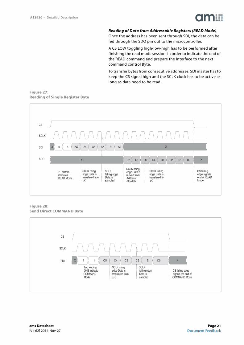
Reading of Data from Addressable Registers (READ Mode). Once the address has been sent through SDI, the data can be fed through the SDO pin out to the microcontroller.
A CS LOW toggling high-low-high has to be performed after finishing the read mode session, in order to indicate the end of the READ command and prepare the Interface to the next command control Byte.
To transfer bytes from consecutive addresses, SDI master has to keep the CS signal high and the SCLK clock has to be active as long as data need to be read.
Figure 27:Reading of Single Register Byte
Figure 28:Send Direct COMMAND Byte
CS
SCLK
SDI 0 1 A5 A4 A3 A2 A1 A0 XX
SCLK rising edge Data is moved from Address <A5-A0>
Channel Amplifier and Frequency DetectorThe channel amplifier consists of a variable gain amplifier (VGA), an automatic gain control, and a frequency detector. The latter detects the presence of a carrier. As soon as the carrier is detected the AGC is enabled, the gain of the VGA is reduced and set to the right value and the RSSI can be displayed.
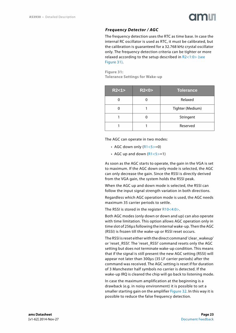
Frequency Detector / AGCThe frequency detection uses the RTC as time base. In case the internal RC oscillator is used as RTC, it must be calibrated, but the calibration is guaranteed for a 32.768 kHz crystal oscillator only. The frequency detection criteria can be tighter or more relaxed according to the setup described in R2<1:0> (see Figure 31).
Figure 31:Tolerance Settings for Wake-up
The AGC can operate in two modes:
• AGC down only (R1<5>=0)
• AGC up and down (R1<5>=1)
As soon as the AGC starts to operate, the gain in the VGA is set to maximum. If the AGC down only mode is selected, the AGC can only decrease the gain. Since the RSSI is directly derived from the VGA gain, the system holds the RSSI peak.
When the AGC up and down mode is selected, the RSSI can follow the input signal strength variation in both directions.
Regardless which AGC operation mode is used, the AGC needs maximum 35 carrier periods to settle.
The RSSI is stored in the register R10<4:0>.
Both AGC modes (only down or down and up) can also operate with time limitation. This option allows AGC operation only in time slot of 256μs following the internal wake-up. Then the AGC (RSSI) is frozen till the wake-up or RSSI reset occurs.
The RSSI is reset either with the direct command 'clear_wakeup' or 'reset_RSSI'. The 'reset_RSSI' command resets only the AGC setting but does not terminate wake-up condition. This means that if the signal is still present the new AGC setting (RSSI) will appear not later than 300μs (35 LF carrier periods) after the command was received. The AGC setting is reset if for duration of 3 Manchester half symbols no carrier is detected. If the wake-up IRQ is cleared the chip will go back to listening mode.
In case the maximum amplification at the beginning is a drawback (e.g. in noisy environment) it is possible to set a smaller starting gain on the amplifier Figure 32. In this way it is possible to reduce the false frequency detection.
Antenna DamperThe antenna damper allows the chip to deal with higher field strength, it is enabled by register R1<4>. It consists of shunt resistors which degrade the quality factor of the resonator by reducing the signal at the input of the amplifier. In this way the resonator sees a smaller parallel resistance (in the band of interest) which degrades its quality factor in order to increase the linear range of the channel amplifier (the amplifier doesn't saturate in presence of bigger signals). Figure 33 shows the bit setup.
Demodulator / Data SlicerThe performance of the demodulator can be optimized according to bit rate and preamble length as described in Figure 34 and Figure 35.
Figure 34:Bit Setup for Envelop Detector for Different Symbol Rates
If the bit rate gets higher, the time constant in the envelop detector must be set to a smaller value. This means that higher noise is injected because of the wider band. The next table is a rough indication of how the envelop detector looks like for different bit rates. By using proper data slicer settings it is possible to improve the noise immunity paying the penalty of a longer preamble. In fact if the data slicer has a bigger time constant it is possible to reject more noise, but every time a transmission occurs, the data slicer need time to settle. This settling time will influence the length of the preamble. Figure 35 gives a correlation between data slicer setup and minimum required preamble length.
Figure 35:Bit Setup for Data Slicer for Different Preamble Length
Note(s): These times are minimum required, but it is recommended to prolong the preamble.
The comparator of the data slicer can work only with positive or with symmetrical threshold R3<6>. In addition the threshold can be 20 or 40 mV R3<7>. In case the length of the preamble is an issue the data slicer can also work with an absolute threshold R1<7>. In this case the bits R3<2:0> would not influence the performance. It is even possible to reduce the absolute threshold in case the environment is not particularly noisy R2<7>.
CorrelatorAfter frequency detection the data correlation is only performed if the correlator is enabled (R1<1>=1).
The data correlation consists of checking the presence of a preamble (ON/OFF modulated carrier) followed by a certain pattern.
After the frequency detection the correlator waits 16 bits (see bit rate definition in Figure 36) and if no preamble is detected the chip is set back to listening mode and the false wake-up register (R13<7:0>) is incremented by one.
To get started with the pattern correlation the correlator needs to detect at least 4 bits of the preamble (ON/OFF modulated carrier).
The bit duration is defined in the register R7<4:0>(Figure 36) as function of the Real Time Clock (RTC) periods.
If the preamble is detected correctly the correlator keeps searching for a data pattern. The duration of the preamble plus the pattern should not be longer than 40 bits (see bit rate definition in Figure 36). The data pattern can be defined by the user and consists of two bytes which are stored in the registers R5<7:0> and R6<7:0>. The two bytes define the pattern consisting of 16 half bit periods. This means the pattern and the bit period can be selected by the user. The only limitation is that the pattern (in combination with preamble) must obey Manchester coding and timing. It must be noted that according to Manchester coding a down-to-up bit transition represents a symbol "0", while a transition up-to-down represents a symbol "1". If the default code is used (96 [hex]) the binary code is (10 01 01 10 01 10 10 01). MSB has to be transmitted first.
The user can also select (R1<2>) if single or double data pattern is used for wake-up. In case double pattern detection is set, the same pattern has to be repeated 2 times.
Additionally it is possible to set the number of allowed missing zero bits (not symbols) in the received bitstream (R2<6:5>), as shown in the Figure 37.
Figure 37:Allowed Pattern Detection Errors
If the pattern matches the wake-up, interrupt is displayed on the WAKE output.
If the pattern detection fails, the internal wake-up (on all active channels) is terminated with no signal sent to MCU and the false wake-up register will be incremented (R13<7:0>).
The wake-up state is terminated with the direct command ‘clear_wake’ (see Figure 24). This command terminates the MCU activity. The termination can also be automatic in case there is no response from MCU. The time out for automatic termination is set in a register R7<7:5>, as shown in theFigure 38.
In case the data correlation is disabled (R1<1>=0) the AS3930 wakes up upon detection of the carrier frequency only as shown in Figure 39. In order to ensure that AS3930 wakes up the carrier burst has to last longer than 550 μs. To set AS3930 back to listening mode there are two possibilities: either the microcontroller sends the direct command clear_wake via SDI or the time out option is used ( R7<7:5>). In case the latter is chosen, AS3930 is automatically set to listening mode after the time defined in T_OUT ( R7<7:5>), counting starts at the low-to-high WAKE edge on the WAKE pin.
Single Pattern DetectionThe Figure 40 shows the wake-up protocol in case the pattern correlation is enabled (R1<1>=1) for a 125 kHz carrier frequency. The initial carrier burst has to be longer than 550 μs and can last maximum 16 bits (see bit rate definition in Figure 36). If the ON/OFF mode is used ( R1<5>=1), the minimum value of the maximum carrier burst duration is limited to 10 ms. This is summarized in Figure 41. In case the carrier burst is too long the internal wake-up will be set back to low and the false wake-up counter (R13<7:0>) will be incremented by one.
The carrier burst must be followed by a preamble (0101... modulated carrier with a bit duration defined in Figure 36) and the wake-up pattern stored in the registers R5<7:0> and R6<7:0>. The preamble must have at least 4 bits and the preamble duration together with the pattern should not be longer than 40 bits. If the wake-up pattern is correct, the signal on the WAKE pin goes high one bit after the end of the pattern and the data transmission can get started. To set the chip back to listening mode the direct command clear_wake, as well as the time out option ( R7<7:5>) can be used.
Figure 40:Wake-up Protocol Overview with Single Pattern Detection
False Wake-up RegisterThe wake-up strategy in the AS3930 is based on 2 steps:
1. Frequency Detection: In this phase the frequency of the received signal is checked.
2. Pattern Correlation: Here the pattern is demodulated and checked whether it corresponds to the valid one.
If there is a disturber or noise capable to overcome the first step (frequency detection) without producing a valid pattern, then a false wake-up call happens.Each time this event is recognized a counter is incremented by one and the respective counter value is stored in a memory cell (false wake-up register). Thus, the microcontroller can periodically look at the false wake-up register, to get a feeling how noisy the surrounding environment is and can then react accordingly (e.g. reducing the gain of the LNA during frequency detection, set the AS3930 temporarily to power down etc.), as shown in the Figure 42. The false wake-up counter is a useful tool to quickly adapt the system to any changes in the noise environment and thus avoid false wake-up events.
Most wake-up receivers have to deal with environments that can rapidly change. By periodically monitoring the number of false wake-up events it is possible to adapt the system setup to the actual characteristics of the environment and enables a better use of the full flexibility of AS3930.
Figure 42:Concept of the False Wake-up Register Together with System
Real Time Clock (RTC)The RTC can be based on a crystal oscillator (R1<0>=1), the internal RC-oscillator (R1<0>=0), or an external clock source (R1<0>=1). The crystal has higher precision of the frequency but a higher current consumption and needs three external components (crystal plus two capacitors). The RC-oscillator is completely integrated and can be calibrated if a reference signal is available for a very short time to improve the frequency accuracy. The calibration gets started with the trim_osc direct command. Since no non-volatile memory is available the calibration must be done every time after the RCO was turned OFF. The RCO is turned OFF when the chip is in power down mode, a POR happened, or the crystal oscillator is enabled. Since the RTC defines the time base of the frequency detection, the selected frequency (frequency of the crystal oscillator or the reference frequency used for calibration of the RC oscillator) should be about one forth of the carrier frequency:
Where:
FCAR is the carrier frequency
FRTC is the RTC frequency
Note(s): The third option for the RTC is the use of an external clock source, which must be applied directly to the XIN pin (XOUT floating).
To trim the RC-Oscillator, set the chip select (CS) to high before sending the direct command trim_osc over SDI. Then 65 digital clock cycles of the reference clock (e.g. 32.768 kHz) have to be sent on the clock bus (SCLK), as shown in Figure 45. After that the signal on the chip select (CS) has to be pulled down.
The calibration is effective after the 65th reference clock edge and it will be stored in a volatile memory. In case the RC-oscillator is switched OFF or a power-ON-reset happens (e.g. battery change) the calibration has to be repeated.
Figure 45:RC-Oscillator Calibration via SDI
External Clock SourceTo clock the AS3930 with an external signal the crystal oscillator has to be enabled (R1<0>=1). As shown in the Figure 4 the clock must be applied on the pin XIN while the pin XOUT must stay floating. The RC time constant has to be 100μs with a tolerance of ±10% (e.g. R=680 kΩ and C=22pF). In the Figure 46 the clock characteristics are summarized.
Parameter Conditions Min Typ Max Units
Frequency If no calibration is performed 27 32.768 42 kHz
If calibration is performed 31 32.768 34.5 kHz
Calibration time Periods of reference clock 65 cycles
1. Dimensions and tolerancing conform to ASME Y14.5M-1994.
2. All dimensions are in millimeters. Angles are in degrees.
3. Dimension b applies to metallized terminal and is measured between 0.25mm and 0.30mm from terminal tip. Dimension L1 represents terminal full back from package edge up to 0.15mm is acceptable.
4. Coplanarity applies to the exposed heat slug as well as the terminal.
RoHS: The term RoHS compliant means that ams AG products fully comply with current RoHS directives. Our semiconductor products do not contain any chemicals for all 6 substance categories, including the requirement that lead not exceed 0.1% by weight in homogeneous materials. Where designed to be soldered at high temperatures, RoHS compliant products are suitable for use in specified lead-free processes.
ams Green (RoHS compliant and no Sb/Br): ams Green defines that in addition to RoHS compliance, our products are free of Bromine (Br) and Antimony (Sb) based flame retardants (Br or Sb do not exceed 0.1% by weight in homogeneous material).
Important Information: The information provided in this statement represents ams AG knowledge and belief as of the date that it is provided. ams AG bases its knowledge and belief on information provided by third parties, and makes no representation or warranty as to the accuracy of such information. Efforts are underway to better integrate information from third parties. ams AG has taken and continues to take reasonable steps to provide representative and accurate information but may not have conducted destructive testing or chemical analysis on incoming materials and chemicals. ams AG and ams AG suppliers consider certain information to be proprietary, and thus CAS numbers and other limited information may not be available for release.
Copyright ams AG, Tobelbader Strasse 30, 8141 Unterpremstaetten, Austria-Europe. Trademarks Registered. All rights reserved. The material herein may not be reproduced, adapted, merged, translated, stored, or used without the prior written consent of the copyright owner.
Devices sold by ams AG are covered by the warranty and patent indemnification provisions appearing in its General Terms of Trade. ams AG makes no warranty, express, statutory, implied, or by description regarding the information set forth herein. ams AG reserves the right to change specifications and prices at any time and without notice. Therefore, prior to designing this product into a system, it is necessary to check with ams AG for current information. This product is intended for use in commercial applications. Applications requiring extended temperature range, unusual environmental requirements, or high reliability applications, such as military, medical life-support or life-sustaining equipment are specifically not recommended without additional processing by ams AG for each application. This product is provided by ams AG “AS IS” and any express or implied warranties, including, but not limited to the implied warranties of merchantability and fitness for a particular purpose are disclaimed.
ams AG shall not be liable to recipient or any third party for any damages, including but not limited to personal injury, property damage, loss of profits, loss of use, interruption of business or indirect, special, incidental or consequential damages, of any kind, in connection with or arising out of the furnishing, performance or use of the technical data herein. No obligation or liability to recipient or any third party shall arise or flow out of ams AG rendering of technical or other services.
Information in this datasheet is based on product ideas in the planning phase of development. All specifications are design goals without any warranty and are subject to change without notice
Preliminary Datasheet Pre-Production
Information in this datasheet is based on products in the design, validation or qualification phase of development. The performance and parameters shown in this document are preliminary without any warranty and are subject to change without notice
Datasheet Production
Information in this datasheet is based on products in ramp-up to full production or full production which conform to specifications in accordance with the terms of ams AG standard warranty as given in the General Terms of Trade
Datasheet (discontinued) Discontinued
Information in this datasheet is based on products which conform to specifications in accordance with the terms of ams AG standard warranty as given in the General Terms of Trade, but these products have been superseded and should not be used for new designs
1 General Description1 Key Benefits & Features2 Applications
4 Pin Assignments4 16-pin TSSOP5 QFN 4x4 16 LD
6 Absolute Maximum Ratings7 Electrical Characteristics10 Typical Operating Characteristics
12 Detailed Description13 Operating Modes13 Power Down Mode13 Listening Mode13 Standard Listening Mode13 ON/OFF Mode (Low Power mode )14 Preamble Detection / Pattern Correlation14 Data Receiving15 System and Block Specification15 Main Logic and SDI16 Register Table Description and Default Values18 Serial Data Interface (SDI)22 SDI Timing22 Channel Amplifier and Frequency Detector23 Frequency Detector / AGC24 Antenna Damper25 Demodulator / Data Slicer26 Correlator29 Wake-up Protocol - Carrier Frequency 125 kHz29 Without Pattern Detection30 Single Pattern Detection32 False Wake-up Register33 Real Time Clock (RTC)33 Crystal Oscillator34 RC-Oscillator34 External Clock Source


![Programming and Interfacing Guide - ScioSense...Programming and Interfacing Guide CCS811 Programming guide ams Application Note Page 2 [v2-00] 2017-Sep-26 Document Feedback Content](https://static.documents.pub/doc/80x56/60f6c596329dbc0a591877d2/programming-and-interfacing-guide-sciosense-programming-and-interfacing-guide.jpg)


