+ All Categories
Home > Documents > ASIP DATA-PLANE PROCESSOR FOR MULTI-STANDARD …

ASIP DATA-PLANE PROCESSOR FOR MULTI-STANDARD …

Date post: 23-Feb-2022
Category:
Upload: others
View: 1 times
Download: 0 times
Share this document with a friend
96
ASIP DATA-PLANE PROCESSOR FOR MULTI-STANDARD WIRELESS PROTOCOL PROCESSING BY MOHIT GOPAL WANI A thesis submitted to the Graduate School—New Brunswick Rutgers, The State University of New Jersey in partial fulfillment of the requirements for the degree of Master of Science Graduate Program in Electrical and Computer Engineering Written under the direction of Prof. Predrag Spasojevi´ c and approved by New Brunswick, New Jersey October, 2010
Transcript

ASIP DATA-PLANE PROCESSOR FOR

MULTI-STANDARD WIRELESS PROTOCOL

PROCESSING

BY MOHIT GOPAL WANI

A thesis submitted to the

Graduate School—New Brunswick

Rutgers, The State University of New Jersey

in partial fulfillment of the requirements

for the degree of

Master of Science

Graduate Program in Electrical and Computer Engineering

Written under the direction of

Prof. Predrag Spasojevic

and approved by

New Brunswick, New Jersey

October, 2010

c© 2010

Mohit Gopal Wani

ALL RIGHTS RESERVED

ABSTRACT OF THE THESIS

ASIP Data-plane Processor for Multi-Standard Wireless

Protocol Processing

by Mohit Gopal Wani

Thesis Director: Prof. Predrag Spasojevic

Evolving Multi-Protocol Multi-Band Software Defined Radio (SDR) devices aim at sup-

porting multiple protocols seamlessly and efficiently. The design of such radios necessi-

tates flexibility in physical layer processing, flexibility in routing packets through pro-

cessing engines and flexibility in radio frequency reception/transmission. This disserta-

tion addresses an efficient implementation of flexible physical layer processing (PHY) for

Interleaving, De-Interleaving and linear Minimum Mean Square Error (MMSE) detec-

tion in Multiple Input Multiple Output (MIMO) receivers through Application Specific

Instruction Set Processors (ASIPs). The thesis defines and develops a WINLAB cog-

nitive radio (WiNC2R) compatible data-plane ASIP architecture along with suitable

hardware-software partitioning of the Processing Engine unit.

Given the requirement of very significant design time and the lack of the flexibil-

ity after design, dedicated ASIC for PHY may not be a viable option although it has

the best performance among all available options. The software application running

on general purpose processor cannot satisfy the throughput requirements of the wire-

less standards. ASIPs provide a better trade-off between flexibility and performance,

with the advantage of considerably lower design time than ASICs. We design an effi-

cient multi-standard (802.11a, 802.16e/m) supporting Interleaver/De-Interleaver ASIP,

ii

satisfying the throughput requirements for all the modulation-schemes/data-rates in

both of the standards. It can be programmed to scale for supporting future wireless

standards (that use Block Interleaving/De-Interleaving). We also study viability of a

flexible MIMO MMSE detector ASIP supporting variable MR (Number of receiving

antennas) * MT (Number of transmitting antennas) operations. We have analyzed the

implementation of an hardware-centric algorithm for MIMO detection on an ASIP and

also improved its performance with the help of techniques such as fixed point imple-

mentation, Single Instruction Multiple Data (SIMD) and Very Long Instruction Word

(VLIW). Analysis of the design performance results for MIMO ASIP indicates the lim-

itations of hardware-implementation-specific algorithms on ASIP. We also provide the

account of design decisions such as custom ports, memory interfaces and registers that

are added to the data-plane processor ASIPs in order to substitute them for dedicated

hardware engines in the WiNC2R platform.

iii

Acknowledgements

First, I would like to thank my advisors Prof. Zoran Miljanic and Prof. Predrag

Spasojevic for their continuous support, vision, guidance and encouragement in the

development of this thesis work. I am indebted to them for their confidence about

my work in this challenging area in the intersection of communication processing and

computer architecture fields. They gave me complete freedom in my work, although I

had to literally start without any substantial background in both of the areas. Many

thanks to them for clarifying my concepts from time to time and for the care they

provided throughout the period.

I am thankful to Jerry Redington (Tensilica, Inc.) for his patient support. The thesis

was not possible without getting the insights of computer architecture from Jerry. I

was lucky to have him as someone whom I can approach for any silly doubt on Tensilica

architecture. I would also like to thank Khanh Le for all those brainstorming sessions

and lively discussions that helped me getting better in understanding the hardware

design. I truly appreciate his readiness to help anytime, be it related to this project or

otherwise. Thanks to Ivan Seskar for providing help whenever requested for.

It was an enjoyable experience to work with WINLAB mates: Akshay, Onkar, Mad-

hura, Prashant and VLSI-lab mates: Wen and Raghuveer. I thank them for their

friendship and support. Special thanks to Chandru for providing daily rides to WIN-

LAB and helping me numerous times during my entire stay at Rutgers.

Most importantly, I would like to thank my parents, Mrs. Lata Wani and Mr.

Gopal Wani, my brother Mr. Milind Wani and sister Mrs. Meghana Amritkar, for

always supporting me in all my pursuits academic, personal or otherwise. My every

success, big or small, is owed to their love, support and sacrifices.

iv

Table of Contents

Abstract . . . . . . . . . . . . . . . . . . . . . . . . . . . . . . . . . . . . . . . . ii

Acknowledgements . . . . . . . . . . . . . . . . . . . . . . . . . . . . . . . . . iv

List of Tables . . . . . . . . . . . . . . . . . . . . . . . . . . . . . . . . . . . . . viii

List of Figures . . . . . . . . . . . . . . . . . . . . . . . . . . . . . . . . . . . . ix

1. Introduction . . . . . . . . . . . . . . . . . . . . . . . . . . . . . . . . . . . 1

1.1. Software Defined Radio . . . . . . . . . . . . . . . . . . . . . . . . . . . 2

1.2. Implementation of Software Defined Radio . . . . . . . . . . . . . . . . . 3

1.3. WiNC2R Architecture . . . . . . . . . . . . . . . . . . . . . . . . . . . . 5

2. Data-Plane Processor . . . . . . . . . . . . . . . . . . . . . . . . . . . . . . 8

2.1. Introduction . . . . . . . . . . . . . . . . . . . . . . . . . . . . . . . . . . 8

2.1.1. Data Plane . . . . . . . . . . . . . . . . . . . . . . . . . . . . . . 8

2.1.2. Control Plane . . . . . . . . . . . . . . . . . . . . . . . . . . . . . 9

2.1.3. ASIP as a Data Plane Processor . . . . . . . . . . . . . . . . . . 10

2.1.3.1. ASIPs and Other Microprocessors . . . . . . . . . . . . 12

2.1.3.2. Advantages of ASIPs . . . . . . . . . . . . . . . . . . . 13

2.1.3.3. Place of Data Plane Processors in Programmable Radio

Platforms . . . . . . . . . . . . . . . . . . . . . . . . . . 14

2.2. Tensilica Xtensa ASIP architecture . . . . . . . . . . . . . . . . . . . . . 14

2.2.1. Why Tensilica Processor? . . . . . . . . . . . . . . . . . . . . . . 17

2.3. Configurability . . . . . . . . . . . . . . . . . . . . . . . . . . . . . . . . 18

2.4. The ASIP Design Cycle . . . . . . . . . . . . . . . . . . . . . . . . . . . 19

v

3. Processing Engine . . . . . . . . . . . . . . . . . . . . . . . . . . . . . . . . 22

3.1. Virtual Flow Description . . . . . . . . . . . . . . . . . . . . . . . . . . . 24

3.2. Integration of ASIP based PE into WiNC2R platform . . . . . . . . . . 25

3.2.1. Designing ASIP Processor for dedicated PE framework: Method-

ology . . . . . . . . . . . . . . . . . . . . . . . . . . . . . . . . . . 26

3.2.2. Communicating with the outside logic . . . . . . . . . . . . . . . 27

3.2.2.1. Import wires . . . . . . . . . . . . . . . . . . . . . . . . 27

3.2.2.2. Interrupts . . . . . . . . . . . . . . . . . . . . . . . . . . 28

3.2.2.3. Export States . . . . . . . . . . . . . . . . . . . . . . . 30

3.2.2.4. Queues . . . . . . . . . . . . . . . . . . . . . . . . . . . 30

3.2.3. Memories . . . . . . . . . . . . . . . . . . . . . . . . . . . . . . . 32

3.3. Software application flow . . . . . . . . . . . . . . . . . . . . . . . . . . 33

4. ASIP for Multi-Standard Interleaving and De-Interleaving . . . . . . 36

4.1. PHY description . . . . . . . . . . . . . . . . . . . . . . . . . . . . . . . 36

4.2. Interleaving algorithm . . . . . . . . . . . . . . . . . . . . . . . . . . . . 37

4.2.1. Algorithm Improvement . . . . . . . . . . . . . . . . . . . . . . . 41

4.3. De-Interleaving algorithm . . . . . . . . . . . . . . . . . . . . . . . . . . 45

4.3.1. Algorithm Improvement . . . . . . . . . . . . . . . . . . . . . . . 46

4.4. Cost benefit analysis . . . . . . . . . . . . . . . . . . . . . . . . . . . . . 49

4.4.1. Conclusion . . . . . . . . . . . . . . . . . . . . . . . . . . . . . . 54

5. ASIP for MIMO MMSE Detection . . . . . . . . . . . . . . . . . . . . . 55

5.1. MIMO systems introduction . . . . . . . . . . . . . . . . . . . . . . . . . 55

5.2. MIMO MMSE detection requirements and algorithm . . . . . . . . . . . 56

5.3. Implementation on ASIP . . . . . . . . . . . . . . . . . . . . . . . . . . . 58

5.3.1. Complexity analysis and Performance improvement analysis . . . 68

5.3.2. Cost Analysis . . . . . . . . . . . . . . . . . . . . . . . . . . . . . 70

5.4. Conclusion . . . . . . . . . . . . . . . . . . . . . . . . . . . . . . . . . . 71

vi

6. Conclusion and Future Work . . . . . . . . . . . . . . . . . . . . . . . . . 79

6.1. Future work . . . . . . . . . . . . . . . . . . . . . . . . . . . . . . . . . . 80

Glossary . . . . . . . . . . . . . . . . . . . . . . . . . . . . . . . . . . . . . . . . 81

References . . . . . . . . . . . . . . . . . . . . . . . . . . . . . . . . . . . . . . . 83

vii

List of Tables

3.1. Control Options for Interrupt/Polling facilitator module . . . . . . . . . 29

5.1. Complexity Analysis of MIMO MMSE detection using Burg’s algorithm 58

viii

List of Figures

1.1. WiNC2R top level SoC view . . . . . . . . . . . . . . . . . . . . . . . . . 6

2.1. Control-Plane vs. Data-Plane . . . . . . . . . . . . . . . . . . . . . . . . 9

2.2. Classification of Microprocessors . . . . . . . . . . . . . . . . . . . . . . 13

2.3. Data Plane Processors in WiNC2R Layered Radio Architecture . . . . . 15

2.4. Processor Design Space - Baseline Options . . . . . . . . . . . . . . . . . 17

2.5. How a custom instruction is added in ASIP . . . . . . . . . . . . . . . . 20

2.6. ASIP design algorithm . . . . . . . . . . . . . . . . . . . . . . . . . . . . 21

3.1. Functional Unit Architecture . . . . . . . . . . . . . . . . . . . . . . . . 23

3.2. Processing Engine Architecture . . . . . . . . . . . . . . . . . . . . . . . 24

3.3. Tensilica ASIP Interface . . . . . . . . . . . . . . . . . . . . . . . . . . . 28

3.4. Interrupt and Polling facilitator Module . . . . . . . . . . . . . . . . . . 29

3.5. Output Queue Data Format . . . . . . . . . . . . . . . . . . . . . . . . . 31

3.6. Custom ports declaration in TIE . . . . . . . . . . . . . . . . . . . . . . 32

3.7. Instructions for accessing custom ports . . . . . . . . . . . . . . . . . . . 32

3.8. Memory map for Tensilica ASIP based functional units . . . . . . . . . . 33

3.9. Software flow on the ASIP . . . . . . . . . . . . . . . . . . . . . . . . . . 34

3.10. ASIPs in WiNC2R SoC . . . . . . . . . . . . . . . . . . . . . . . . . . . 35

4.1. 802.11a Transmitter Block Diagram . . . . . . . . . . . . . . . . . . . . 37

4.2. 802.11n Transmitter Block Diagram . . . . . . . . . . . . . . . . . . . . 38

4.3. 802.16e/m Transmitter Block Diagram . . . . . . . . . . . . . . . . . . . 39

4.4. WiFi (802.11a) and WiMax (802.16e/m) Details . . . . . . . . . . . . . 39

4.5. Interleaving: Bit Shuffling in the Register Matrix . . . . . . . . . . . . . 40

4.6. A custom instruction removing bottleneck in the interleaving algorithm 42

4.7. Interleaving application performance gain (in multiple times) . . . . . . 43

ix

4.8. Interleaving application: Performance improvement of Matrix Writing

function and Matrix shuffling (processing) function . . . . . . . . . . . . 44

4.9. Custom instructions’ impact on the CPI (Interleaving application) . . . 45

4.10. Custom instruction for filling registers row-wise . . . . . . . . . . . . . . 47

4.11. After processing, rearrangement of bits for reading out . . . . . . . . . . 48

4.12. De-Interleaving application performance gain (in multiple times) . . . . 49

4.13. De-Interleaving application: Performance improvement of Matrix writing

function and Matrix shuffling (processing) function . . . . . . . . . . . . 50

4.14. Custom instructions’s impact on the CPI (De-Interleaving application) . 51

4.15. A snippet of custom instruction filling the register matrix . . . . . . . . 52

4.16. Snippet of instruction scheduling through TIE . . . . . . . . . . . . . . . 53

4.17. Comparison of custom hardware addition cases . . . . . . . . . . . . . . 53

4.18. ASIP performance in MIPS . . . . . . . . . . . . . . . . . . . . . . . . . 54

5.1. MIMO System . . . . . . . . . . . . . . . . . . . . . . . . . . . . . . . . 55

5.2. VLIW logical layer . . . . . . . . . . . . . . . . . . . . . . . . . . . . . . 64

5.3. Snapshot of instructions on 3 issue VLIW processor . . . . . . . . . . . 65

5.4. SIMD implementation using state registers . . . . . . . . . . . . . . . . 66

5.6. MIMO Application Performance (4x4 Matrix) . . . . . . . . . . . . . . . 76

5.7. Gain in MIMO Application Performance (4x4 Matrix) . . . . . . . . . . 76

5.8. MIMO Application Performance (2x2 Matrix) . . . . . . . . . . . . . . . 77

5.9. Gain in MIMO Application Performance (2x2 Matrix) . . . . . . . . . . 77

5.10. 4x4 MIMO MMSE ASIP area trend-details . . . . . . . . . . . . . . . . 78

5.11. Flexible MIMO MMSE ASIP area analysis . . . . . . . . . . . . . . . . 78

x

1

Chapter 1

Introduction

This section briefly provides overview of the idea of Cognitive Radio (CR) and in general

Software Defined Radio (SDR) devices, requirements and trends in their architectures.

We also discuss about WiNLAB Network Centric Cognitive Radio (WiNC2R) platform

architecture with detailed view of the Virtual Flow Pipelining concept.

The objective of cognitive radio is to solve spectrum scarcity problem by means

of dynamic spectrum access. A Cognitive Radio (CR) is required to constantly sense

its environment and dynamically reconfigure its own parameters so as to communi-

cate reliably and efficiently. It should be able to alter its transmission rate, power,

frequency, modulation scheme and any combination of these to support wireless stan-

dards throughput requirements. The switching between the available channels across

different standards should be transparent to the user and fast enough to have no data

loss [1].

The main features of Cognitive Radios are listed below [2].

• Spectrum Sensing: A CR scans a wide spectrum and determine frequencies being

used as well as determines its own transmission characteristics

• Policy and configuration: A CR is subject to certain policies in each of the en-

vironment which it should adhere to and has configuration setting pertaining to

each of the policy.

• Modular architecture: CR should have modular level architecture within which

they can direct the flow of data dynamically

• Application oriented profiles: CRs can Create/maintain application specific (ex-

ample: long distance, moving with high speed etc.) profiles and incorporate those

2

transparent to the user

• Adaptive algorithms: CRs switch operating algorithms to improve their efficiency

of a network collectively.

• Distributed collaboration: CRs share their knowledge of operating environment

and application requirements, to determine policies for optimal network resources

utilization.

• Security: The security of the data won’t be compromised while CRs entering or

leaving network.

Cognitive radios are estimated to be useful in number of applications such as:

• Spectrum sensing and frequency adaptive abilities are useful where guaranteed

communication links are a necessity

• Flexibility to support various communication technologies is big advantage for

military applications

• Multiple Networks supporting ability can serve as a bridge between two devices/

networks based on different communication standards

• CRs can create separate user profiles which suite applications in specific environ-

ments and hence useful for providing location dependent services

• CR is always a secondary user if the spectrum is licensed even though it can sense

a free portion of spectrum and tune to it. This feature avoids priority conflicts

and leads to efficient network utilization.

1.1 Software Defined Radio

Software Defined Radio (SDR) is a technology that enables reconfigurable system for

wireless networks. SDR defines a combination of hardware and software technologies on

which the radios operating functions are implemented [3]. Cognitive Radio sits above

the SDR and lets it determine which mode of operation and parameters to choose [4].

3

1.2 Implementation of Software Defined Radio

There are several requirements that are identified for a SDR architecture as defined in

[5]:

• SDR platforms usually consists of a combination of different processing devices

such as Field Programmable Gate Arrays (FPGA), Digital Signal Processors (DSPs),

General Purpose Processors (GPPs), programmable System on Chip (SoC) or

other application specific programmable processors. The use of these technolo-

gies allows new wireless features and capabilities to be added to existing radio

systems without requiring new hardware. Thus a component model defining se-

mantics of components, the interfaces and the protocols for managing information

exchange is necessary.

• The flows should be developed independent of the platform since there may be

several platform under different application requirements. This independence also

assumes a common operational environment from the platforms.

• Launching of an application requires finding, loading, and instantiating each in-

dividual component on the appropriate device of the platform, connecting the

components (virtually) and performing any initialization tasks necessary to have

application running properly. There should be a module/processor for launching

the application.

• The applications should be stored in some kind of memory. Hence, there should

be a way to store, organize and access memory.

• There should be a communication mechanism (transport layer) to exchange in-

formation and data across different nodes in the platform.

• A mechanism (manager) is needed to manage and keep track of all the hardware

and software resources and provide interface with the user.

• There should be a way to interact with the heterogeneous hardware components

to configure them and facilitate control/data information exchange.

4

• The validation of platform’s capacity and available resources (capacity model) is

required for each application to be supported

• The flexibility of:

– Per packet selection that is required in computationally intensive PHY pro-

cessing

– Interoperability

– Support of new protocols that are in development and will emerge with the

completely new applications domain

Traditional SDR platforms consist of General Purpose Processors and DSP Proces-

sors which are inadequate for future high data-rate communications in terms of pro-

cessing speed and energy efficiency. The advances in VLSI technology has directed the

future development of SDR platforms towards Multi-Processor System-on-Chip (MP-

SoC) based platforms consisting of several heterogeneous processors tailored for differ-

ent processing tasks. A number of MPSoC based architectures have been proposed till

date. [6] proposes MPSoC where number of processing elements (GPP/ DSP/ ASIC/

reconfigurable hardware units are inter-connected to the Network-on-Chip (NoC). Both

the Programs running on each of the processing elements as well as flows between them

are dynamically configured at run-time. [7] describes a design paradigm for extensible

SDR architecture for including support for newer protocols. But it cannot dynamically

(per packet seamless) support multiple protocols. [8] has described an SDR architecture

where four processing engines (2-LIW processor with 32 bit SIMD ALU and local mem-

ory), a global memory and one Control processor (ARM) is connected to a central bus.

The powerful PEs offer performance for compute-intensive tasks (WCDMA, 2MHz).

However the architecture is not enough for supporting higher data-rates required in

WiFi and WiMax standards. [9] describes fine grain processing reconfigurable FPGA-

like fabrics connected through arrays. These are difficult to program for achieving

throughput.

The processing complexity of wireless protocol experiences the Compound Annual

Growth Rate (CAGR) of 78, while the SOC performance is increasing at CAGR of 22

5

[10]. This necessitates novel network centric architecture solutions that will suffice new

processing paradigms. WiNC2R is one of such solutions [1].

1.3 WiNC2R Architecture

Winlab Network Centric Cognitive Radio (WiNC2R)[1] is a programmable MPSoC

(based on hardware assisted virtualization) SDR platform. It is aimed at providing

a high performance platform for experimentation with various adaptive wireless net-

work protocols ranging from simple etiquettes to more complex ad-hoc collaboration.

It is designed for flexible processing of both Physical and MAC/network layers with

sustained bit rates of 10 MBpS and higher with adaptability to variety of network

interference conditions and protocol conditions. This is step towards an architecture

that will be scalable to adapt to future throughput increases, modifications of radio

and higher layers and complexity requirements of portable and fixed devices.

WinC2R is based on the concept of Virtual Flow Pipelining (VFP) [10] where the

underlying PHY resources are hidden from the higher network layers. It consists of mul-

tiple clusters, each made up of several heterogeneous Processing Engines(ASIPs, RTL

modules and Software entities running on GPP) connected via hierarchical AMBA AXI

bus. Each cluster has a VFP local-function module, while the centralized VFP Con-

troller is connected to the central AXI bus along with a global control memory structure

called as Global Task Table (GTT). Figure 1.1 shows the top level SoC architectural

view. The key features of platform are:

• Virtualization technique [10] is introduced to provide common interface to higher

layers which will hide the necessary details for resource reservations and sharing.

• Dynamic sharing of bandwidth is observed in IP packet based world by following

Service Level Agreement (SLA) Parameters.

• The allocations of the ’resources-share’ to the flow create the virtual flow consist-

ing of the sequence of the processing steps on the required processing modules.

• Resource scheduler takes care of full flow latency requirements of wireless protocol

6

Figure 1.1: WiNC2R top level SoC view

Source: Onkar Sarode. WinC2R architecture document (Centralized UCM arch.vsd),www.svn.winlab.rutgers.edu/cognitive, March 2010

processing

• The virtualization layer handles hardware resources to manage communication

bandwidth with responsibility for SLA reinforcement among sessions and pro-

tecting each of them.

• Each session treats its share of the physical bandwidth as a separate channel.

Virtual Flow consists of a set of functions and their scheduling requirements asso-

ciated with a higher protocol entity (application, session, IP or MAC address). VFP

functions are executed as tasks, where task can run on potentially multi functional

hardware engines or software programmable CPUs. VFP controller is responsible for

selecting each step of the task function and its associated parameters on each of the

processing engines. The sequencing is enforced by ordering, function (or thread on

CPU) selection and synchronization between processing units. The data flow paths

can be configured during the setup and initialization and also during the actual op-

eration. WiNC2R provides a backbone architecture with a uniform interface to all

7

modules, which supports plug-and-play ability. WiNC2R also supports run time re-

configurability inside the modules currently implemented.

The thesis focuses on designing the Application Specific Instruction Set Processors

(ASIPs) to be plugged as data-plane processors in VFP based programmable frame-

work of WiNC2R platform. Chapter 2 presents a detailed account of data-plane pro-

cessors. We will analyze the features of several processors design choices. Chapter 3

presents the architectural customizations of the ASIP for porting into the WiNC2R

platform. It also gives the account of architectural decisions and hardware-software

partitioning. Chapter 4 includes the design and performance improvement achieved

through Instruction Set Architecture (ISA) extensions for the processing engines of

Interleaving/De-Interleaving. Chapter 5 illustrates the analysis of implementation of

hardware-centric algorithm for MIMO MMSE detection. Chapter 5 also gives details

about the steps involved in the algorithm improvement, with the use of VLIW/ SIMD

techniques and other processor customizations. Chapter 6 completes the thesis work

by providing conclusion and future work.

8

Chapter 2

Data-Plane Processor

This section provides the background of concepts: data-plane processing and Applica-

tion Specific Instruction Set Processors. We also discuss the trade-offs of using ASIPs

as data-plane processors, with the comparison of options such as general purpose RISC

processors and dedicated ASIC implementations. This also includes general discussion

about processor design and ASIP design aspects.

2.1 Introduction

Multi-core System on Chips (SoCs) have become prominent in the high performance

real-time systems. The decision about the right kinds of processors to be put in to

this multi-processor chip is based on the concept of presence of two planes in the

design: Control plane and Data plane. In a typical SoC, control plane manages the

user interface, the system synchronization, and few more functions while the data plane

processing manages compute intensive tasks [11]. A tighter integration of these planes

is necessary for achieving optimal performance. Figure 2.1 shows the clear distinction

between these planes.

2.1.1 Data Plane

In networking or communications systems, the data plane processes each packet as it

passes through the system [12]. Data-plane tasks may include converting packets from

one protocol to another, encrypting or decrypting data, filtering unwanted packets, pri-

oritizing packets, routing them to their next destination and computational processing

of the physical layer. In short, all the data-intensive operations are carried out by data

plane. Data plane typically uses specialized CPUs (lacking caches and with limited

9

Figure 2.1: Control-Plane vs. Data-Plane

Source: http://www.tensilica.com

memory size) or Application Specific Integrated Circuits (ASIC) or dedicated FPGA

processing unit. A small local memory holds instructions, limiting the available code

space, often to several thousand instructions. These engines may include special in-

structions to extract and manipulate fields of arbitrary bit length, as these operations

are useful in some packet protocols. Short pipelines can be advantageous in data-plane

processing. Clock rates are often modest (1GHz or less) to minimize power dissipation.

They may include accelerators to offload specific tasks.

2.1.2 Control Plane

The control plane handles packets that require extra processing, user interface, higher

levels of protocol stacks, system synchronization and all other non-data intensive appli-

cations [11]. Moreover control plane handles the tasks of configuring data-plane layer

and managing the data-flow. The control plane typically uses standard General Pur-

pose Processors (GPP) since they are easily programmable. Control plane software

is designed assuming it will be running on a general purpose processor. It has fewer

computations and more conditional branches than typical applications. Hence, it will

perform better with short pipeline (small branch prediction penalty).

The control plane and data plane can share the same memory space to reduce cost and

eliminate the latency in moving the data across memories. Data-plane processors archi-

tecture and analysis is the focus of this research thesis. The data-plane engines can be

10

organized in two ways [12]. In a parallel model, one CPU is designated as the master,

receiving all packets and assigning them to engines as needed. The data-plane engines

can be arranged in a pipeline. For example, the first engine could classify packets, the

second could perform filtering, the third could perform encapsulations, and the fourth

could perform traffic management. It also ensures proper ordering and deterministic

latency.

2.1.3 ASIP as a Data Plane Processor

System developers are working to significantly reduce the resource levels required to

develop systems by making it easier to design the chips in those systems and also to

make SOCs sufficiently flexible so that every new system design does not require a

new SOC design. Hence, the data plane processor design is facing a very strong push

towards higher flexibility and computational requirements with power consumption

constraints. The algorithmic requirements are increasing at far higher rate than that of

architectural improvements to support it [13]. The important characteristics of ASIPs

from an algorithmic perspective are:

1. Highly regular computation intensive operations;

2. Considerable I/O /memory accesses;

3. Complicated controlling in less computationally intensive tasks.

The limits on the general purpose processor performance due to instruction level par-

allelism and power consumption in the compute intensive applications (that require

flexibility also) have given rise to an interesting idea. The idea is to take a general

purpose processor and improve its performance by moving often executed sequences

(functions) into a special hardware execution units requiring only one instruction to

implement such a function. The result is Application Specific Instruction-set Proces-

sors (ASIPs) which can perform specific tasks as efficiently as possible [14]. ASIP design

is a promising technique to meet the performance and cost goals of high-performance

systems. In recent years, ASIPs have become popular because they simultaneously

11

offer high performance and short design cycles. In contrast to off-the-shelf processor

cores, ASIPs include dedicated functional units and ISA customizations that speed up

execution of the ’hot spots’ in a given application. Whereas, they cannot offer the same

performance as ASICs due to limitations imposed by micro architectural constraints

and the tighter control exerted for the data movement in the processors. Dedicated

hardware is also cheaper in terms of cost and power as compared to ASIPs.

The programmability of ASIPs enables a larger volume, as multiple related ap-

plications, as well as different generations of an application can be mapped onto the

same ASIP. A programmable solution also provides a much lower risk as well as a pre-

dictable and shorter time-to-market solution since writing and debugging software is

cheaper than designing, debugging and manufacturing working hardware [15]. ASIPs

allow designers to extend the base processor with custom instructions, memories, ports

and even VLIW/SIMD extensions, making possible the best performance possible with

processor-centric implementation. Given the high customization in ASIPs, they have

essentially created a class for ’Data-plane Units’ (DPUs).

Hardwired RTL design has many attractive characteristics: small area, low power,

and high throughput. With the advent of multi million-gate SOCs, RTLs have become

difficult to design and have issues such as slow verification, and poor scalability for

increasingly complex problems. ASIP is a design methodology that retains most of

RTLs benefits while reducing design time and risk. ASIPs can implement data-path

operations that closely match those of RTL functions. The functional equivalents of

RTL logic blocks are implemented using application-specific processors by adding exe-

cution units to the processors existing integer pipeline, additional registers and register

files to the processors state, additional I/O ports, and other functions as needed by the

specific application.

Due to the high degree of specialization, there will be dedicated processors for dif-

ferent application domains like digital video, wireless communication, multimedia, etc.

Quantitative analysis has been done in [16], that shows energy efficiency measured in

mega-operations/instructions per mW (MOpS/mW) for different architectures running

the same benchmark along-with area required for each of the architectures. It shows

12

that there is roughly one order in magnitude of energy efficiency between a RISC em-

bedded processor, a domain specific DSP, and an ASIP optimized for this particular

benchmark. Also proved is a fact that in terms of architectural choices of flexibility

and efficiency, ASIP provides a best compromise between flexibility and performance.

2.1.3.1 ASIPs and Other Microprocessors

The microprocessors can be classified [17] on the basis of:

1. The Hardware (ISA) micro architecture:

• Reduced Instruction Set Computer (RISC)

• Complex Instruction Set Computer (CISC)

• Very Large Instruction Word (VLIW)

• Superscalar

2. Characteristics of the Application Areas

• General Purpose Processor (GPP)/ Micro-controller

• Special purpose processor (SPP)

– Application Specific Integrated Circuit (ASIC)

– Application Specific Instruction Set Processor (ASIP)

– Digital Signal Processor (DSP)

The classification of Microprocessors is also shown in the Figure 2.2.

The specialized nature of individual embedded applications creates two issues for

general-purpose processors in data-intensive embedded applications [18]. First, there is

a poor match between the critical functions needed by many embedded applications and

a fixed-ISA processor’s basic integer instruction set and register file. As a result of this

mismatch, these critical embedded applications often require an unacceptable number of

computation cycles when run on general-purpose processors. Second, narrowly focused,

low-cost embedded devices cannot take full advantage of a general-purpose processor’s

broad capabilities. Consequently, expensive silicon resources built into the processor

13

Figure 2.2: Classification of Microprocessors

Original concept: Daniel Kastner. Lecture on Embedded systems. 2002-2003

are wasted in these applications because they are not needed by the specific embedded

tasks assigned to the processor.

An ASIP sits between the high efficiency of an ASIC and the low cost of a GPP

and provides a good balance of hardware and software to meet requirements such as

flexibility, performance, fast time to market and power consumption.

2.1.3.2 Advantages of ASIPs

The benefits of ASIPs are [13]:

• Non permanent customization and application development after fabrication

• Time to market considering evolving requirements and new applications/ideas

• Economies of scale

• Flexible I/O and Interface functionality required for embedded systems

14

• Supports refinement and co-design of hardware and software, as well as behavior

and architecture

• All important metrics including Power-Delay-Area perspective are considered con-

tinuously in the design phase

These ASIP advantages do not come free but with certain disadvantages such as

2.1.3.3 Place of Data Plane Processors in Programmable Radio Platforms

New Multiprocessor System-on-Chip (MPSoC) based platforms are being defined at the

architecture - micro-architecture boundary which are inevitable for complex communi-

cation systems of the future. The goals are how to simultaneously optimize flexibility,

cost , energy and performance. System-on-Chip development has fostered platform as

well as communication based design [13]. These platforms tend to be component-based

and aim at providing a range of choices from custom structures to fully programmable

solutions at various cost-benefit ratios. There are two types of platforms: Software

platforms and Hardware platforms. Software platforms run the application on gen-

eral processor and offer maximum flexibility while the Hardware platforms are limited

in terms of flexibility but much faster in processing. In these platforms, application-

architectural exploration is focal part of implementation methodology.

WiNC2R [1] is such a programmable platform where ASIPs/ASICs are used as

data-plane processors providing an additional degree of freedom in functional process-

ing. Data-plane processors are essentially multi-standard protocol processing engines

in WiNC2R SoC platform. Figure 2.3 shows the data plane processors in WiNC2R

architecture.

We have designed the data-plane processors for WiNC2R platform using Tensilica

Xtensa R© ASIPs. The next section gives details of the Xtensa ASIP architecture.

2.2 Tensilica Xtensa ASIP architecture

The Xtensa architecture is highly flexible due to configurability. The following aspects

of the processor can be configured at the build time:

15

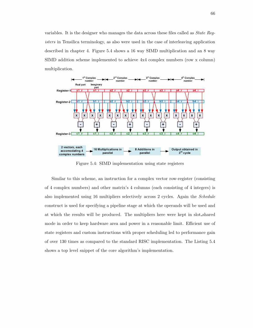
Figure 2.3: Data Plane Processors in WiNC2R Layered Radio Architecture

Base source: Onkar Sarode. Scalable VFP-SoC architecture poster at WINLAB-IAB,Dec.2009. Modified here to show control plane, data-plane and place of ASICs/ASIPs

• Core micro-architecture

• Core instructions (Width, floating point instructions, DSP instructions)

• Co-processors

• Memory system

– Caches

– Processor interface

– Local memories

• Exceptions and Interrupts

• Test and debug

The basic architecture can be pruned or augmented depending on the data processing

performance requirement of the application. The native processor pipeline is five stage

(or seven stage) pipelined architecture. The five stage pipeline has stages:

I: Instruction fetch

R: Register read

16

E: Execute

M: Memory write

W: Register write-back

The core pipeline is augmented or additional pipeline is added through the Tensilica

Instruction Extension (TIE) language defined instructions, optimizing the target algo-

rithm’s performance.

Extensive architecture exploration and refinement process is needed to realize an

optimal architecture for a given set of applications. Specifically following aspects in the

design space are to be taken into consideration [16].

1. Instruction Set: The degree of parallelism in the application code that can be

explored by the instruction-set using VLIW (Very Long Instruction-Word) in-

structions as well as the definition of special purpose instructions to accelerate

specific portions of the application code while reducing power consumption.

2. The processor micro-architecture: This includes definitions of instruction and

data pipelines, bypassing logic as well as the memory subsystem to reduce data

and instruction access latencies.

3. Implementation of the Processor: A reasonable estimate of on power consumption,

clock frequency and gate count can be gathered after a synthesis run with the

target technology. The design decisions would need to be revisited if any of the

parameters are out of the specification range.

4. System impact on the processor’s performance: The system behavior and in-

teraction with the processor has an immediate impact on the optimal processor

micro-architecture. For ex. If the shared memory is going to be shared by a

number of processors, it would be wise to have sufficient data-cache included in

the architecture.

For Tensilica xtensa processors, the baseline processor design-space is illustrated in

Figure 2.4.

17

Figure 2.4: Processor Design Space - Baseline Options

Original concept: Heinrich Meyr. System-on-Chip for Communications: The Dawn ofASIPs and the Dusk of ASICs, IEEE Workshop on Signal Processing Systems (SIPS),Seoul, Korea, 2003. (Modified here with respect to Tensilica Xtensa context)

2.2.1 Why Tensilica Processor?

Following points are precisely the reason for choosing Tensilica processors.

• Processors are modifiable through

– Instruction Sets

∗ Can simultaneously issue 24 bit and 16 bit instructions. If extended for

VLIW, it can issue 32 bit TIE instructions along with basic 16 and 24

bit instructions

– Processor I/O ports - to exactly match extensive computational application

needs

∗ Local and system interfaces

∗ Designer defined I/O interfaces

• Possibility for multi-processor design

– Availability of Single and Double precision floating point co-processors

– Availability of DSP specific Vectra processor

18

• Defining scheduling of extended instructions is possible

• Provided tools for design environment for:

– Multi-Processor System-on-Chip (MPSoC) architecture

– Exploration of design space for Cache and memory parameters such as lo-

cality, associativity etc.

– Simultaneous power analysis for variety of configurations

• Tensilica Instruction Extension (TIE) language is similar to Verilog HDL and

hence easier to learn if Verilog is familiar

• Multi Issue VLIW technology: The base LX3 processor can be configured as

3-issue VLIW (Flexible Length Instructions (FLIX)) processor

Since any set of DSP operations can be encapsulated into custom instructions, cus-

tomized Xtensa LX cores are capable of outperforming most DSPs and general-purpose

processors on most of DSP applications [19]. Custom instructions target a specific

application. An Xtensa LX may be more area-efficient than a processor core that at-

tempts to perform well on a wide range of applications but is only used for one specific

application.

2.3 Configurability

There are several approaches to a configurable processor design [19]:

• Manually inserting instructions (hand-coded RTL ) into the RTL description of

the processor

– Cannot guarantee operational correctness of the manually inserted instruc-

tions

– Associated software tools will not know about manually inserted instruc-

tions and hence they cannot exploit the instructions. Hence, ASIC firmware

developers have to write assembly function calls and subroutines to exploit

such instructions.

19

• Use specialized language to define the custom processor extensions

– Facilitates the high-level specification of new data-path functions in the form

of new processor instructions, registers, register files, I/O ports, and FIFO

queue interfaces.

– A configurable processor can implement wide, parallel, and complex data-

path operations that closely match those used in custom RTL hardware.

The equivalent data-paths are implemented by augmenting the base proces-

sor’s integer pipeline with additional execution units, registers, and other

functions developed by the chip architect for a target application.

The later option is widely used nowadays. The customized configuration is architected

through:

• Selecting from standard configuration options, such as bus widths, interfaces,

memories, and pre-configured execution units (floating-point units, DSPs, etc)

[19].

• Adding new registers, register files, and custom task-specific instructions that

support specialized data types and operations. If a custom instruction is added

to the xtensa processor, the execution logic and register files are added in the data-

path as can be seen from Figure 2.5. In this figure, the blue path denotes the base

pipeline of the processor whereas the orange portion denotes the custom data-path

created due to addition of custom instructions and supplimentary register files.

• Using programs that automatically analyze the C code and determine the best

processor configuration and ISA (instruction-set architecture) extensions

2.4 The ASIP Design Cycle

Here onwards, the terminology ’ASIP’ will be used interchangeably with ’Tensilica

Xtensa LX2/LX3’ processor. The Figure 2.6 illustrates the design methodology for

the ASIP design. The decisions such as whether to have SIMD/VLIW or only manual

20

Figure 2.5: How a custom instruction is added in ASIP

Source: Tensilica Xtensa LX2 product documentation

instructions to be inserted etc. depend completely on the kind of application to be

executed and power/area/frequency budget of the SoC. Once built, the processor can

be co-simulated with external RTL logic and SystemC simulation models to gauge

the performance of the complete SoC. The configuring of baseline processor has been

explained earlier in Figure 2.4 on Page 17. When the potential custom instructions

are decided, the register file and functions that can be called from custom instructions,

also need to be considered. Moreover depending on the memory load/store operation

frequency more custom/user registers may be included.

21

Figure 2.6: ASIP design algorithm

22

Chapter 3

Processing Engine

In this section, we discuss about the Processing Engine present in WiNC2R architecture.

We also discuss issues that were handled in the transition from dedicated hardware

processing engine architecture to ASIP-based architecture, the account of decisions

made and strategy adopted to have an efficient transition.

The WiNC2R platform is a cluster-based System-on-Chip (SoC) architecture where

each cluster contains a group of Functional Units (FUs) connected by low hierarchy

AMBA-AXI bus. Each of the FU is responsible for certain step in protocol processing

and is specific for that step. As shown in Figure 1.1 the clusters are connected through

centralized AMB-AXI bus. FUs are autonomous units of the SoC engaged by event

driven mechanisms. The reconfigurability of the data-flow is achieved using two memory

structures: Global Task-descriptor Table (GTT) and Task-Descriptor (TD) table [20]

[21]. GTT is connected to central AMBA AXI bus while TD table is present in each

of the FU respectively. Both of these tables are configured by the software for setting

up the flows. The processing in FU can be divided into two parts; data processing

and control processing. The data processing includes the core radio signal processing

functionality while the control processing is to achieve flexibility in the flow. FUs are

implemented in:

1. Register Transfer Logic (RTL) using hardware description languages: VHDL and

Verilog

2. Application Specific Instruction Set Processors (ASIPs)

3. C functions called through DPI interface in System Verilog logic block

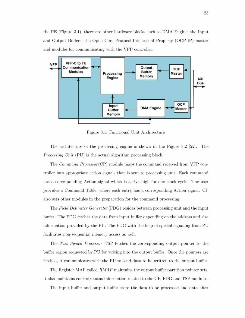
The Processing Engine (PE) forms the core computing block inside a FU. Alongside

23

the PE (Figure 3.1), there are other hardware blocks such as DMA Engine, the Input

and Output Buffers, the Open Core Protocol-Intellectual Property (OCP-IP) master

and modules for communicating with the VFP controller.

Figure 3.1: Functional Unit Architecture

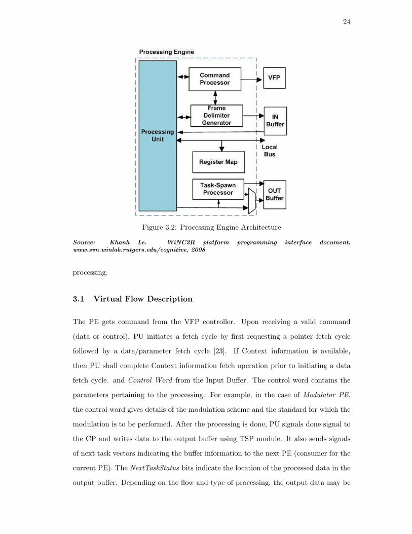
The architecture of the processing engine is shown in the Figure 3.2 [22]. The

Processing Unit (PU) is the actual algorithm processing block.

The Command Processor(CP) module maps the command received from VFP con-

troller into appropriate action signals that is sent to processing unit. Each command

has a corresponding Action signal which is active high for one clock cycle. The user

provides a Command Table, where each entry has a corresponding Action signal. CP

also sets other modules in the preparation for the command processing.

The Field Delimiter Generator(FDG) resides between processing unit and the input

buffer. The FDG fetches the data from input buffer depending on the address and size

information provided by the PU. The FDG with the help of special signaling from PU

facilitates non-sequential memory access as well.

The Task Spawn Processor TSP fetches the corresponding output pointer to the

buffer region requested by PU for writing into the output buffer. Once the pointers are

fetched, it communicates with the PU to send data to be written to the output buffer.

The Register MAP called RMAP maintains the output buffer partition pointer sets.

It also maintains control/status information related to the CP, FDG and TSP modules.

The input buffer and output buffer store the data to be processed and data after

24

Figure 3.2: Processing Engine Architecture

Source: Khanh Le. WiNC2R platform programming interface document,www.svn.winlab.rutgers.edu/cognitive, 2008

processing.

3.1 Virtual Flow Description

The PE gets command from the VFP controller. Upon receiving a valid command

(data or control), PU initiates a fetch cycle by first requesting a pointer fetch cycle

followed by a data/parameter fetch cycle [23]. If Context information is available,

then PU shall complete Context information fetch operation prior to initiating a data

fetch cycle. and Control Word from the Input Buffer. The control word contains the

parameters pertaining to the processing. For example, in the case of Modulator PE,

the control word gives details of the modulation scheme and the standard for which the

modulation is to be performed. After the processing is done, PU signals done signal to

the CP and writes data to the output buffer using TSP module. It also sends signals

of next task vectors indicating the buffer information to the next PE (consumer for the

current PE). The NextTaskStatus bits indicate the location of the processed data in the

output buffer. Depending on the flow and type of processing, the output data may be

25

stored at more than one location. The NextTaskRequest signal indicates the VFP Task

Termination (TT) block how the output data at locations indicated by status bits is

to be processed. The TT processing includes transferring the data to next FU/FUs in

the data flow. The NT Request tells the TT to which FU the data is to be sent.

3.2 Integration of ASIP based PE into WiNC2R platform

The most important issue while designing SDR based devices is flexibility along with

efficiency. The RTL design is certainly not flexible to add newer standards/protocols

on ad-hoc basis due to huge design time. Naturally to satisfy the programmability

requirement and also maintain a comparable performance, ASIP was considered as a

logical alternative. The design migrating from RTL to firmware control has following

implications [18]:

1. Flexibility: The block’s function can be changed or newer functions can be added

through firmware.

2. Sophisticated and low-cost software development methods can be used to develop

and debug most of the chip features

3. Faster system modeling is possible with the help of higher abstract description

and simulation ability

4. Control and Data processing is now integrated into the processor, which is easier

to manage

5. Design productivity increases due to processor-based SOC design approach, since

it sharply reduces risks of fatal logic bugs and permits graceful recovery when a

bug is discovered

For WiNC2R PHY layer functions, ASIP is handled at SoC architecture level and

programming model is maintained same as hardware based Processing Engines. To

augment the platform with processor-centric PEs, we had to deal with mainly the

following issues:

26

• An optimal combination of partitioned hardware and software is required. Some

of the functionality for supporting hardware in PE can be moved to software;

• Communication with the other Processing Engines should be transparent to them

and without hampering the performance;

• Memory organization: An optimal instruction and data memory size should be

chosen so as to accommodate all current and future application needs;

• Possibility of general enhancement to Xtensa architecture for one PHY function

proving useful for other PHY function;

• Strategies to achieve an optimal context switching between different tasks;

• Analysis of achievable throughput on ASIP implementation. For example in the

case of MIMO MMSE detection PE as explained in chapter 5, we had to sacrifice

precision accuracy since the throughput with floating point implementation was

outside acceptable rate.

3.2.1 Designing ASIP Processor for dedicated PE framework: Method-

ology

The CP module as explained in the earlier section, is responsible for interfacing with the

VFP controller, setting up other modules present in PE for data processing and mapping

the data/control command (sent by VFP) to action signals (sent to PU). The processor

(with the help of custom ports to be added) and programmable interrupt/exception

architecture would be able to communicate efficiently with the VFP controller. Setting

up other modules can also be done in synchronization when the command from VFP

comes. The mapping of the command to action signals can be efficiently done in

software. Hence, it is reasonable to remove the CP unit completely.

The FDG can also be scrapped completely since the ASIP to be substituted in-

herently has load and store unit which can handle data fetching from the input buffer

memory. Similar to FDG, TSP module should also be removed since the processor is

27

capable of storing the processed data into output buffer memory due to presence of

inherent load-store unit.

3.2.2 Communicating with the outside logic

The ASIP base version does not have any custom ports but only general Processor

Interface (PIF) and interrupts/exceptions structure defined at the time of the configu-

ration. The input buffer and output buffer can be connected to a bus where the ASIP

is connected through PIF. With this type of connection, the processor has to go to

the bus every time it wants to fetch the data or send the data. Moreover this scheme

won’t work if it has to send pulse to the outside RTL logic. In that case, there is no

guarantee that the outside RTL logic would receive the response in the definite estimate

of time, due to possible contention on the bus as well as set priorities of incoming and

outgoing data-signals to use the communication resources. All these issues have hin-

dered the inclusion of a general purpose processor in the data-plane of computationally

intensive/real-time systems.

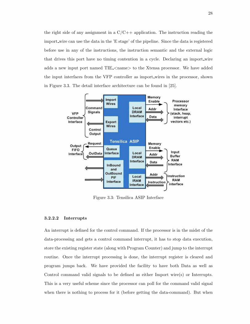
3.2.2.1 Import wires

The inclusion of custom ports for communicating with the external RTL logic is the

only way to solve the above mentioned issues. Xtensa architecture allows the addition

of custom ports the processor interface. To use the external ports, they need to be

defined in the Tensilica Instruction Extension (TIE) language [24] as Operations(custom

instructions) and should be compiled with the desired processor configuration before

start building the configuration. Before describing the details of the interfaces and how

the data is used in the pipeline, we recall the stages in the 5-stage pipelined processor

as described in section 2.1.3.3 on Page 14.

The import wire construct defines an input to the ASIP that can be read by designer-

defined instructions [24]. The import wire is typically to read the status of some external

logic, device, or another processor in a system. The name of the import wire can be

included in the state-interface-list of an operation. The name of the import wire then

becomes a valid variable name inside the operation or semantic body that can appear on

28

the right side of any assignment in a C/C++ application. The instruction reading the

import wire can use the data in the ’E stage’ of the pipeline. Since the data is registered

before use in any of the instructions, the instruction semantic and the external logic

that drives this port have no timing contention in a cycle. Declaring an import wire

adds a new input port named TIE <name> to the Xtensa processor. We have added

the input interfaces from the VFP controller as import wires in the processor, shown

in Figure 3.3. The detail interface architecture can be found in [25].

Figure 3.3: Tensilica ASIP Interface

3.2.2.2 Interrupts

An interrupt is defined for the control command. If the processor is in the midst of the

data-processing and gets a control command interrupt, it has to stop data execution,

store the existing register state (along with Program Counter) and jump to the interrupt

routine. Once the interrupt processing is done, the interrupt register is cleared and

program jumps back. We have provided the facility to have both Data as well as

Control command valid signals to be defined as either Import wire(s) or Interrupts.

This is a very useful scheme since the processor can poll for the command valid signal

when there is nothing to process for it (before getting the data-command). But when

29

it starts processing it can not poll without hampering the performance; and hence

the control command comes as an interrupt although its costlier to implement. The

mapping of either or both of the command valid signals on either interrupt or just

a import wire is achieved with the help of intr poll facilitator block [25]. The Figure

3.4 shows the interrupt facilitator block, while Table 3.1 refers to the programmability

feature of the module.

Figure 3.4: Interrupt and Polling facilitator Module

Table 3.1: Control Options for Interrupt/Polling facilitator module

Case Description RMAP Bits[1:0]

Control-command as interrupt and Data-command polling 00

Control-command as interrupt and Data-command as interrupt 01

Control command as polling and Data-command as interrupt 10

Control command as polling and Data command as polling 11

30

3.2.2.3 Export States

A state defines a construct to create registers where the values are stored prior to the

instruction execution [24]. An instruction can also assign a value to a state, which is

then updated with this new value after the execution of the instruction. Instructions

that provide a well-defined, but general purpose way to read and write states, are

automatically created by the TIE compiler when a state is declared with the optional

argument add read write. When a state is defined with export keyword, it is made

primary output of the processor. The externally visible value on the port changes only

when the architectural value of the state changes. The exact cycle in which the port is

updated (with the value of a recent write to the state) is implementation dependent. To

avoid synchronization problems with the outside logic, base instruction EXTW helps

ensuring that all externally visible actions from earlier instructions from the processor

prior to the EXTW instruction are executed before the pipeline can proceed to the

next instruction. All the signals going to VFP are defined as export states, as shown

in Figure 3.3 on Page 28.

3.2.2.4 Queues

Once the ASIP finishes data-processing, it has to write the processed data into the

output buffer. In order to reduce the time taken by the ASIP for this operation, there

should be no waiting time for the processor to carry out this operation. To achieve this,

we have segregated output buffer from the ASIP by a synchronous First-In First-Out

(FIFO) buffer. The ASIP is connected to the FIFO by a custom interface called Queue.

The data port TIE <name> is the output of the Xtensa processor that is connected to

the data input of the queue and has the same name and width as specified in the queue

declaration. Like any operand input to the processor, a queue read request is issued

in E stage and used in the M stage of the pipeline. For output queue data must be

available in M stage and sent to the output queue in W stage. The width of the queue

interface for the ASIP is kept at 34 bit. The lower 32 bits are used for the data, and

the upper 2 bits are used for controlling purposes indicating either start of the burst

31

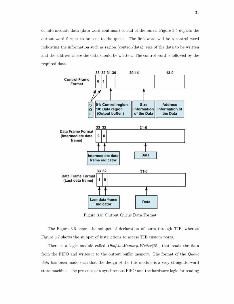
or intermediate data (data word continual) or end of the burst. Figure 3.5 depicts the

output word format to be sent to the queue. The first word will be a control word

indicating the information such as region (control/data), size of the data to be written

and the address where the data should be written. The control word is followed by the

required data.

Figure 3.5: Output Queue Data Format

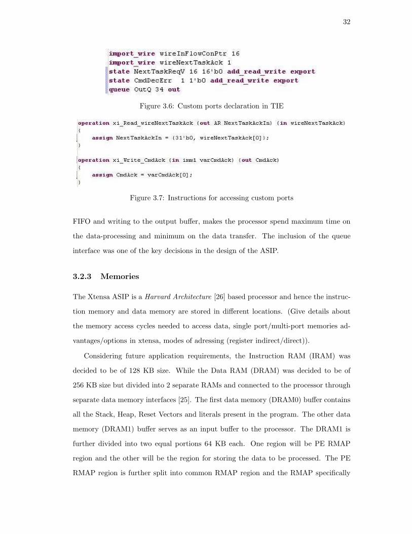
The Figure 3.6 shows the snippet of declaration of ports through TIE, whereas

Figure 3.7 shows the snippet of instructions to access TIE custom ports.

There is a logic module called Obuf to Memory Writer [25], that reads the data

from the FIFO and writes it to the output buffer memory. The format of the Queue

data has been made such that the design of the this module is a very straightforward

state-machine. The presence of a synchronous FIFO and the hardware logic for reading

32

Figure 3.6: Custom ports declaration in TIE

Figure 3.7: Instructions for accessing custom ports

FIFO and writing to the output buffer, makes the processor spend maximum time on

the data-processing and minimum on the data transfer. The inclusion of the queue

interface was one of the key decisions in the design of the ASIP.

3.2.3 Memories

The Xtensa ASIP is a Harvard Architecture [26] based processor and hence the instruc-

tion memory and data memory are stored in different locations. (Give details about

the memory access cycles needed to access data, single port/multi-port memories ad-

vantages/options in xtensa, modes of adressing (register indirect/direct)).

Considering future application requirements, the Instruction RAM (IRAM) was

decided to be of 128 KB size. While the Data RAM (DRAM) was decided to be of

256 KB size but divided into 2 separate RAMs and connected to the processor through

separate data memory interfaces [25]. The first data memory (DRAM0) buffer contains

all the Stack, Heap, Reset Vectors and literals present in the program. The other data

memory (DRAM1) buffer serves as an input buffer to the processor. The DRAM1 is

further divided into two equal portions 64 KB each. One region will be PE RMAP

region and the other will be the region for storing the data to be processed. The PE

RMAP region is further split into common RMAP region and the RMAP specifically

33

pertaining to the respective PE which is substituted by Processor-centric solution, PU-

RMAP. The Output buffer memory is not visible to the processor and hence it won’t

be writing to it directly but via the queue interface to the FIFO. The top level memory

partition is shown in Figure 3.8.

Figure 3.8: Memory map for Tensilica ASIP based functional units

There is no requirement of data-cache in the ASIP as the load handled will be

real time data which is updated in the input buffer continuously. However there is

Instruction cache of size 1KB (2 way set-associative). This is the minimal size possible

and no change in the performance was observed with the size/set associativity was

changed.

3.3 Software application flow

In order to maintain modularity in the software and make it easily extensible, the func-

tions are designed such that replacing few specific functions are needed to change the

kind of PHY application rather than change entire program flow consisting of almost

34

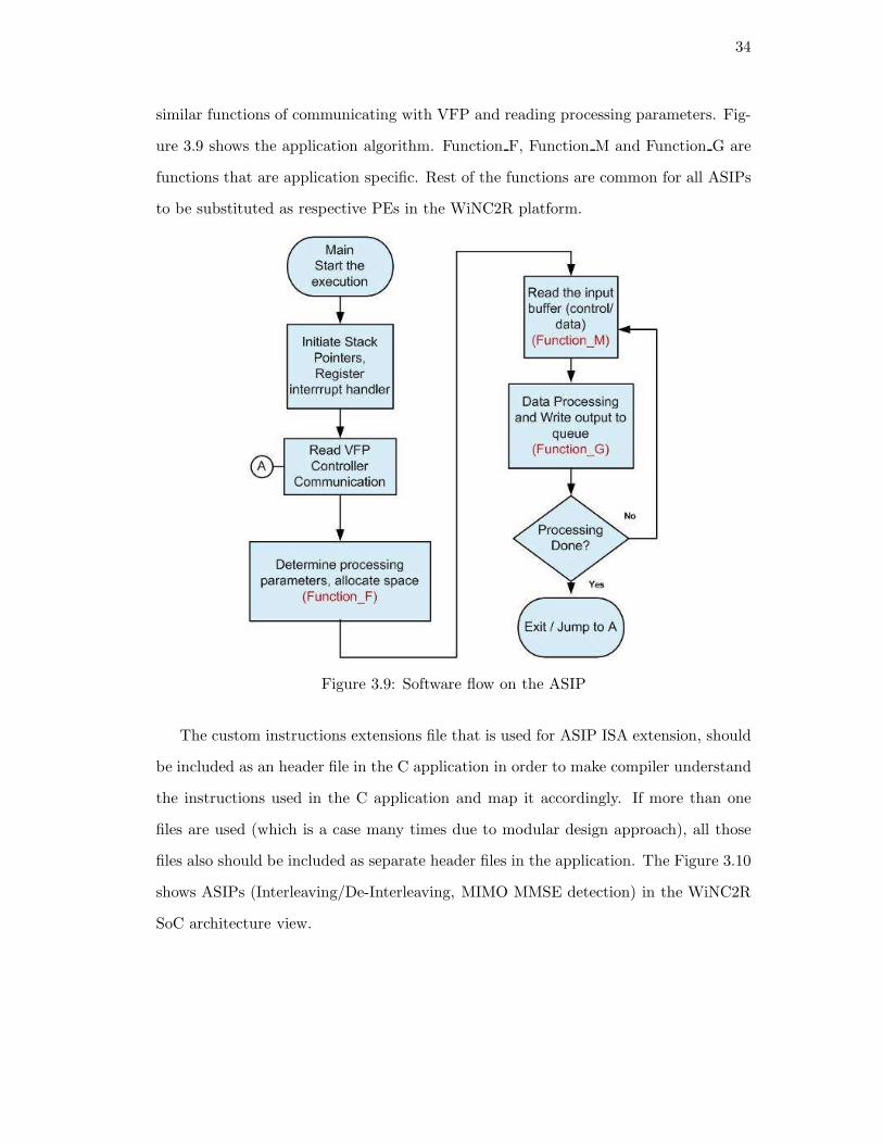
similar functions of communicating with VFP and reading processing parameters. Fig-

ure 3.9 shows the application algorithm. Function F, Function M and Function G are

functions that are application specific. Rest of the functions are common for all ASIPs

to be substituted as respective PEs in the WiNC2R platform.

Figure 3.9: Software flow on the ASIP

The custom instructions extensions file that is used for ASIP ISA extension, should

be included as an header file in the C application in order to make compiler understand

the instructions used in the C application and map it accordingly. If more than one

files are used (which is a case many times due to modular design approach), all those

files also should be included as separate header files in the application. The Figure 3.10

shows ASIPs (Interleaving/De-Interleaving, MIMO MMSE detection) in the WiNC2R

SoC architecture view.

35

Figure 3.10: ASIPs in WiNC2R SoC

Concept: Onkar Sarode. Scalable VFP SoC architecture, Winlab-IAB meet, Dec. 2009.Modified here to include ASIPs of Interleaving/DeIntelreaving and MIMO-MMSE detection

36

Chapter 4

ASIP for Multi-Standard Interleaving and De-Interleaving

In this section, we describe the design of the ASIP. We also describe the performance

vs. cost trade off analysis of the ASIP for multi-standard (Currently 802.11a, 802.11n

[27] and 802.16e/m [28] standards) Interleaving and De-Interleaving operations of the

PHY layer. The ASIP design methodology was highlighted in Figure 2.6 on Page 21.

Accordingly the first step was to study and implement the algorithm on the Xtensa

base processor.

4.1 PHY description

802.11a is IEEE standard for wireless communication. It was adopted first in 1997 and

then revised in 1999. IEEE defines a MAC sublayer, MAC management protocols and

services, and three physical (PHY) layers. The goals of the standard are:

• Deliver services same as found in wired networks

• Guaranteed high throughput

• Provide very reliable data delivery

• Provide continuous network connection

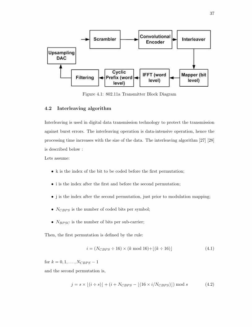
The transmitter block digram for 802.11a is shown in the Figure 4.1.

For 802.11n, the only difference is that there will be multiple streams to be operated

upon simultaneously. These can be handled by having a processor each stream. The

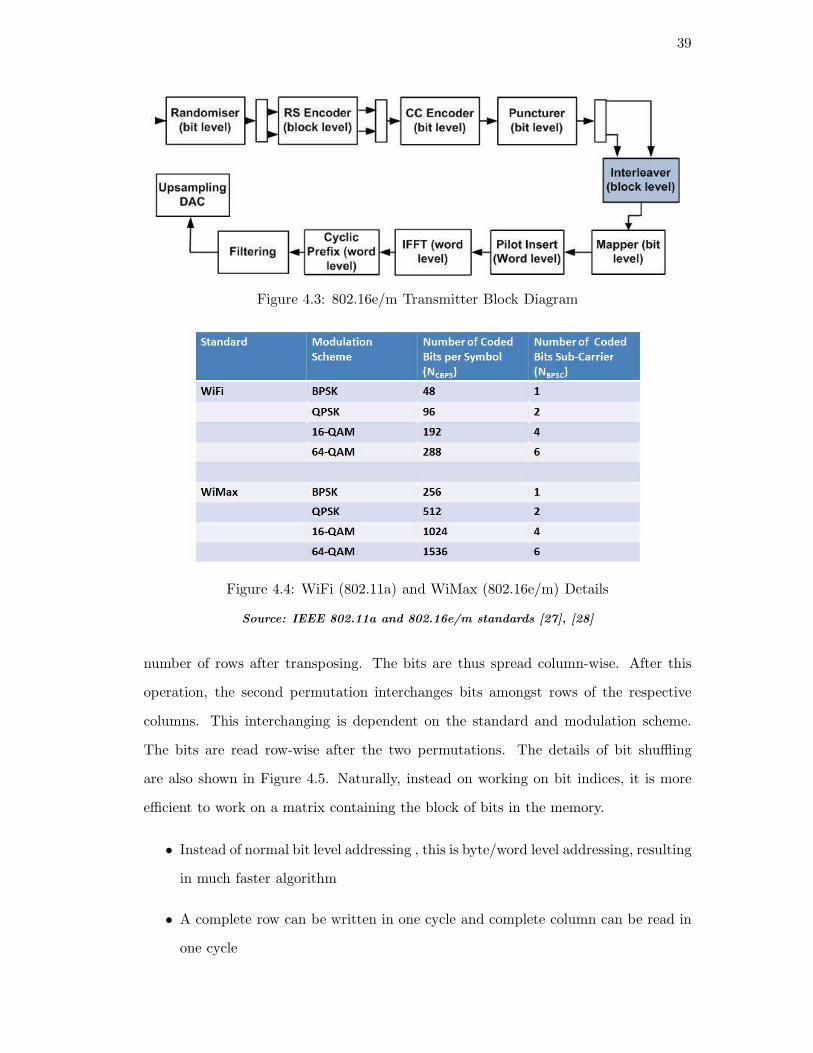
transmitter for 802.11n is shown in the Figure 4.2. Similarly, the 802.16e/m transmitter

is also shown in Figure 4.3.

37

Figure 4.1: 802.11a Transmitter Block Diagram

4.2 Interleaving algorithm

Interleaving is used in digital data transmission technology to protect the transmission

against burst errors. The interleaving operation is data-intensive operation, hence the

processing time increases with the size of the data. The interleaving algorithm [27] [28]

is described below :

Lets assume:

• k is the index of the bit to be coded before the first permutation;

• i is the index after the first and before the second permutation;

• j is the index after the second permutation, just prior to modulation mapping;

• NCBPS is the number of coded bits per symbol;

• NBPSC is the number of bits per sub-carrier;

Then, the first permutation is defined by the rule:

i = (NCBPS ÷ 16)× (k mod 16)+⌊(k ÷ 16)⌋ (4.1)

for k = 0, 1, . . . , NCBPS − 1

and the second permutation is,

j = s× ⌊(i ÷ s)⌋+ (i+NCBPS − ⌊(16 × i/NCBPS)⌋) mod s (4.2)

38

Figure 4.2: 802.11n Transmitter Block Diagram

Source: http://www.wirelessnetdesignline.com, PHY layer tutorial

for i = 0, 1, . . . , NCBPS − 1

where,

s = max(NBPSC ÷ 2, 1) (4.3)

As shown in Equations 4.1 and 4.2, each bit index of the symbol is permuted twice and

the final address is derived. In simple words, the algorithm can be visualized with the

help of a matrix where each element of the matrix contains a bit of the OFDM symbol

[29].

• Number of bits per OFDM symbol depends on the standard (WiFi /WiMax) and

modulation scheme used (BPSK/QPSK/16-QAM/64-QAM) as shown in Figure

4.4

• Matrix has number of rows from 3 to 96 and 16 columns

• Bits are filled row-wise

The first permutation just transposes this matrix. This is a special kind of trans-

posing because the number of rows and columns before transposing remains same as

39

Figure 4.3: 802.16e/m Transmitter Block Diagram

Figure 4.4: WiFi (802.11a) and WiMax (802.16e/m) Details

Source: IEEE 802.11a and 802.16e/m standards [27], [28]

number of rows after transposing. The bits are thus spread column-wise. After this

operation, the second permutation interchanges bits amongst rows of the respective

columns. This interchanging is dependent on the standard and modulation scheme.

The bits are read row-wise after the two permutations. The details of bit shuffling

are also shown in Figure 4.5. Naturally, instead on working on bit indices, it is more

efficient to work on a matrix containing the block of bits in the memory.

• Instead of normal bit level addressing , this is byte/word level addressing, resulting

in much faster algorithm

• A complete row can be written in one cycle and complete column can be read in

one cycle

40

Figure 4.5: Interleaving: Bit Shuffling in the Register Matrix

• Intra-row permutations and Intra-column permutations give possibility to differ-

ent interleaving schemes

• Addressing is taken care of by the processor completely (simpler to implement

with processor than HDL)

The software implementation of this algorithm in C is very inefficient as C cannot

handle bits, rather it can handle character (8 bit wide) / integer (32 bit wide). The

profile analysis of the C application without custom instructions also indicated that the

main bottleneck in the processing is the way the bit-matrix is written into a processor

memory. For filling each element of the matrix (a bit):

1. a LOAD instruction loads the value from input buffer’s indexed address into the

register of the processor

2. since this is a 32 bit wide number, boolean AND instruction is carried out to

mask the other bits with zeros and result is stored in say a1 register

41

3. The data corresponding to the address location of the corresponding matrix ele-

ment’s row is loaded using LOAD into a register say a2

4. a1 and a2 registers are ORred bit-wise

5. the result is stored back into the address of matrix element’s row using STORE

instruction

These instruction sequences are repeated for each vertical-horizontal index combination

of the matrix.

4.2.1 Algorithm Improvement

The solution to this problem would be to have a register matrix inside the ASIP (not

in the memories) and have custom instructions reading the local memory and writing

it to that matrix. Once the matrix is written, the permutation can be done depending

on the protocol. Another custom instruction will read the custom register file and send

the data to the queue interface so that it could be written to the FIFO and then to

the output buffer memory. The first permutation of the algorithm is altogether avoided

if the matrix is written column-wise instead of row-wise. This observation is used

for writing the custom instructions. Hence, the Tensilica Instruction Extension (TIE)

language is used to add:

1. An architecturally visible register file to be a place for storing data-matrix. This

consists of 16 registers each of 32 bit width. This is optimal size to serve the

requirements for all standard and modulation scheme combination with the ex-

ceptions of WiMax-16 QAM and WiMax-64 QAM cases. In these cases, the data

is operated in size of chunks (Chunk size = 16 (Number of state registers) × 32

(Bit-Width of each registers)) and register file is written back again to reutilize

for processing the remaining chunks of the data;

2. Instruction to read the memory and fill the register matrix word-wise;

3. Instruction to read the matrix column(word at a time) and write to the output

queue;

42

4. Instruction to decode standard, modulation scheme information from the control

word;

5. Instructions for writing to custom port queues;

6. Instruction to perform inter-row (same column) permutations.

Some other custom instructions are added in support of the algorithm:

1. Instruction to move lower rows data to upper rows for making it available for

reading

• If only a single row (16-bits) are remaining to be written to output queue,

the 0s are appended (at MSB position) to form a word

2. Instruction to determine the wireless standard and modulation scheme from the

control word

The Figure 4.6 shows how the TIE instruction is removing the bottleneck of the pro-

cessing.

Figure 4.6: A custom instruction removing bottleneck in the interleaving algorithm

43

Cycles taken in the custom case = 16×(Number of cycle to read a memory word)+

16× (Number of cycles to store value from processor register to custom register) +

15× (cycles for incrementing the address pointer).

Cycles taken in the standard case = 16× 32× (Number of cycles to access load

memory word + Number of cycles of boolean AND masking operation + Number of

cycles to load the word from matrix location + Number of cycles for ORring the

result with the current matrix word + Number of cycles for storing the values

in to the matrix in the memory ) As can be seen from above analysis, the sharp gain

in the performance is possible due to presence of custom TIE instructions. The Fig-

ure 4.7 shows the gain in the performance of the complete interleaving operation in

multiple times that of the application running on the standard processor. Thus, in

Figure 4.7: Interleaving application performance gain (in multiple times)

Observed through cycle-accurate simulation

order to support data throughput of 54 MBPS for 802.11a, the required frequency at

which processor need to operate is less than 30 MHz. Such lower frequency is not

imaginable if custom instructions would not have been added. The code size without

custom instruction comes out to be 1348 Bytes and with custom instruction is 1888

bytes, an increase of 40%. With compiler optimization features such as vectorization

and inter-procedural optimization, the cycle count is further reduced by 10% to 15%.

44

The code size is also reduced by 13% to amount 1640 Bytes in case of custom TIE in-

cluded application. The code size is with compiler optimization in normal application

is 1196 Bytes. The graph in Figure 4.8 shows that the gain in writing the matrix block

is at least 32 times that of standard case as also is visible in instructions count analysis

done in the previous part of this subsection. It also shows the gain in the processing

function of the (in this algorithm, processing is nothing but shuffling of data-bits in the

register matrix). The gain is not the correct reflection in the processing operation as

such, since the processing here also includes writing the matrix to the queue output,

which takes multiple cycles.

Figure 4.8: Interleaving application: Performance improvement of Matrix Writing func-tion and Matrix shuffling (processing) function

Observed through cycle-accurate simulation

The addition of custom TIE instructions however does affect the Cycles per In-

struction (CPI) parameter of the processor. As compared to base ISA instructions, the

custom instructions are mostly multi-cycle operations. Hence, the total CPI does get

affected due to the presence of custom instructions, as also visible in graph 4.9. The

increment in CPI is only about 10-15%.

45

Figure 4.9: Custom instructions’ impact on the CPI (Interleaving application)

4.3 De-Interleaving algorithm

De-interleaving is just the opposite process of algorithm. Similar to the case of inter-

leaving, the algorithm operates on bits equal to NCBPS of the respective standard’s

modulation scheme. The Deinterleaving algorithm is explained below: Lets assume:

• j is the index of the original received bit before the first permutation;

• i is the index after the first and before the second permutation;

• k is the index after the second permutation;

• NCBPS is the number of coded bits per symbol;

• NBPSC is the number of bits per sub-carrier;

Then, The first permutation is defined by the rule:

i = s× ⌊j ÷ s⌋+(j + ⌊16× j ÷NCBPS⌋); j = 0, 1, . . . , NCBPS − 1 (4.4)

k = 16× i− (NCBPS − 1)× ⌊(16 × i÷NCBPS)⌋; i = 0, 1, . . . , NCBPS − 1 (4.5)

where, s = max(NBPSC ÷ 2, 1) (4.6)

46

As shown in Equations 4.4 and 4.5, each bit (on the basis of its index) of the symbol

is permuted twice and the original index of the bit is derived. In the same way as

Interleaving, this algorithm can also be visualized with the help of a matrix where each

element of the matrix contains a bit of the OFDM symbol [29].

• Number of bits per OFDM symbol depends on the standard (WiFi /WiMax) and

modulation scheme used (BPSK/QPSK/16-QAM/64-QAM) as shown in Figure

4.4 on Page 39

• Matrix has number of rows from 3 to 96 and 16 columns

• Bits are filled column-wise and read row wise.

To avoid the first permutation, the matrix is filled row-wise. Then inter-row (same-

column) permutations are done. These permutations are exactly opposite to that of

interleaving processing and hence are executed exactly reverse to those shown in Figure

4.5. After this step, the words (each of 32 bit-width) are read row-wise and written to

the output queue interface. The software implementation on the base processor is very

inefficient since the bit handling is highly inefficient through ’C’ using base ISA of a

standard RISC processor.

4.3.1 Algorithm Improvement

Since we have the pre-customized processor (designed for interleaving application) as

a base processor, we have a custom state register matrix available for use for the de-

interleaving application. Also, we want to avoid the first permutation of transposing

the matrix. Considering these factors, following custom instructions are added through

TIE:

1. Reading memory and putting it into state register matrix. For writing row-wise

as shown in Figure 4.10, all state registers have to be the input operand of the

custom instruction. One memory word is used for filling two rows of the matrix

registers. The lower 16 bits go into first row and upper 16 bits go into the row

below. This scheme follows for writing each pair of rows from top to bottom;

47

2. Instruction for bit shuffling (inter-row fashion);

Figure 4.10: Custom instruction for filling registers row-wise

3. Instruction for bit rearrangement. In case the bits do not fill 32 rows, the bits need

to be arranged such that they occupy respective words column wise. See Figure

4.11. This rearrangement of bits facilitates reading out of bit-matrix column by

column.

4. Instruction for reading column-wise (shared with the interleaving case)

With addition of these instructions, the performance gain obtained is shown in

Figure 4.12. The gain is observed in multiple times that of the performance of the

application running on a standard RISC processor. Thus, in order to support data

throughput of 54 MBPS for 802.11a, the required frequency at which processor need

to operate is under 30 MHz. Such lower frequency would not have been imaginable if

custom instructions would not have been added. The lower frequency results in lower

power and hence considerable lower cost of operation. Since the register matrix is

48

Figure 4.11: After processing, rearrangement of bits for reading out

written 2 bit-indexes at a time for each of the register, this operation is quite expensive

as compared filling one register at a time as in the case of interleaving. The performance

gain in this function compared without custom instructions, is depicted in the graph

in Figure 4.13. The performance is improved by 10% to 15% more by using aggressive

compiler otimization which includes automatic vectorization (wherever possible) and

interprocedural optimization. However the lesser performance gain in matrix writing

function is compensated by huge performance gain obtained in shuffling operation. This

is possible since the shuffling is now intra-column and inter-row fashion, and hence

within respective state registers. The code size without custom instructions was 1372

Bytes and rose to 1916 Bytes (39.65% incremenet). With compiler optimization, in the

case of application without custom instructions, the code size remains almost constant

(1364 Bytes), whereas the code size for application with custom instructions, the code

size increases by 19.65% to reach size of 2296 Bytes.

Similar to the case of interleaving, the Cycles per Instruction (CPI) count does

get affected with the use of custom instructions. The graph in Figure 4.14 shows the

comparison of CPIs in both cases.

49

Figure 4.12: De-Interleaving application performance gain (in multiple times)

Observed through cycle-accurate simulation

4.4 Cost benefit analysis

The addition of custom instructions does however add a considerable amount of area to

the base processor. The addition of custom ports needs addition on custom instructions

to access those ports. If they are declared architecturally visible, the XCC compiler

automatically generates RUR.<port-name > as the read instruction and WUR.<port-

name > instruction.

The TIE instructions add considerable area. Since, most of the TIE instructions

added for interleaving are for data shuffling inside the state registers, there is very little

chance of sharing the hardware required across the instructions. The Figure 4.15 shows

a snippet of TIE instruction for filling matrix register (corresponding to de-interleaving

application).

Once the instructions are defined and the corresponding hardware is generated,

several implementations of instructions were carried out to see if they result in overall

lower area. For example, in case of interleaving, initially there were separate instructions

to fill each of the register columns. This combination is checked against the combination

50

Figure 4.13: De-Interleaving application: Performance improvement of Matrix writingfunction and Matrix shuffling (processing) function

Observed through cycle-accurate simulation

where there is a single instruction but with MUXes at the inputs to route appropriate

data to appropriate column of the register-matrix. The area in the later case was found

to be 20% lesser than that of the earlier case. However defining a complex instruction

with lots of muxing does not always help in reduction the area. This was observed in

the case of rearrangement instructions in the de-interleaving processing. Initially, there

were seperate instructions per standard and modulation scheme combination to carry

out rearrangement of bits (rearrangement for WiFi BPSK is explained in Figure 4.11 on

Page 48). All rearrangement instructions were combined next, to check the possibility

of hardware area reduction. But in this case, the area was infact increasing due to the

complex decoding and muxing involved in the combined instruction. Hence, the earlier

option of having separate instructions for each standard- modulation scheme pair was

chosen.

Once the optimal instructions are defined, ’scheduling’ is defined for some of the

custom instructions. Every Custom instruction defined through TIE has an implicit

51

Figure 4.14: Custom instructions’s impact on the CPI (De-Interleaving application)

schedule according to which the reading of the operands and storing of the operation

results into state-registers, queues and register file take place. Schedule is defined in

terms of the pipeline stage depth. The state registers architectural copy is only updated

at the Register Write (RW) stage of the pipeline, even if the implicit schedule defines

the write at earlier stage than RW stage. Hence if the state register is written in earlier

stage than RW stage, multiple (non-architectural) copies of the register are generated

for each stage till RW stage, where the true architectural copy is written. Hence for

reducing area of the TIE instruction with state-register writing operation, generation of

non-architectural copies should be avoided [30]. This is achieved by defining schedule

for writing state registers in the RW stage. In a similar fashion, the operands should be

read as close as to RW stage, to avoid generating multiple copies of the same till ’define’

stage. Figure 4.16 shows a schedule construct defined for matrix filling instruction seen

in Figure 4.15 on Page 52.

The comparison of areas in all of the three case discussed above viz. with only

custom ports, with normal TIE, and TIE with scheduling is shown in the Figure 4.17.

On a base processor of area of 65000 gates, the graph in this figure shows that:

1. With custom ports, 12.12% gate addition is observed over baseline processor

52

Figure 4.15: A snippet of custom instruction filling the register matrix

2. With custom TIE instructions without scheduling defined, 87.32% gate addition

is observed over base processor + custom ports gates area.

3. With custom TIE instructions with scheduling defined, 70.91% gate addition is

observed over base processor + custom ports gate area.

At 65 nm, the gate density1is 854 Kgate/mm2. Hence, the additional hardware

gate area (added for ISA customization) is calculated to be 0.0605 mm2. . We can

get an approximate comparison between ASIP and ASIC-like implementation of multi-

standard interleaving, if we compare custom processor area (baseline processor + logic

added for custom ports + logic added for custom instructions) to that of area required

for custom instruction logic (assumming it will be roughly same as dedicated hardware

implementation).

1Source: TSMC 65nm technology data-sheet, www.tsmc.com

53

Figure 4.16: Snippet of instruction scheduling through TIE

Figure 4.17: Comparison of custom hardware addition cases

Estimate given by Tensilica Xtensa Processor Generator tool

The area of baseline processor + custom ports logic + custom instructions logic

= 65000 + 51683 + 7879 = 124562 gates.

The area of added custom instructions = 51683 + 7879 = 59562 gates.

Rough estimate of the area overhead required for customizable ASIP (with respect

to a dedicated hardware) for multi-standard Interleaving and De-Interleaving

= 109.13%

The Figure 4.18 shows the resultant performance measure in terms of Million In-

structions Per Second (MIPS) count. The performance is calculated for processor run-

ning at 547 MHz frequency (as estimated by Tensilica Xtensa Processor Generator

tool).

54

Figure 4.18: ASIP performance in MIPS

4.4.1 Conclusion

The ASIP designed here satisfies the data-throughput requirement of all of the standard-

modulation scheme combinations in both 802.11a, 802.11n and 802.16e/m standards.

The operating frequency can be kept as low as 30 MHz for the required throughput level.

The custom hardware addition over baseline processor (with custom ports) amounts to

be 70.91%.

55

Chapter 5

ASIP for MIMO MMSE Detection

In this section, we describe the performance vs. cost trade off analysis of the ASIP

for linear Minimum Mean Square Error (MMSE) detection in Multiple Input Multiple

Output (MIMO) OFDM systems. The ASIP is flexible to support number of receiving

antennas (MR) and number of transmitting antennae (MT ) MIMO system. Accordingly

the first step was to study and identify the algorithm to be implemented through ASIP

hardware ad software.

5.1 MIMO systems introduction

MIMO transmission is a technology that is able to increase the spectral efficiency by

transmitting 2 or more data streams on one radio channel, with the use of multiple

antennas at the transmitter. The receiver also has multiple antennas, normally more

than the number of transmitting antennas. This also helps in better quality of service

and high data transmission rate. The high rate is achieved by transmitting multiple data

streams in parallel in the same frequency band and without increasing the bandwidth of

the system. The conceptual diagram of MIMO system is shown in Figure 5.1. The most

Figure 5.1: MIMO System

56

prominent disadvantage of MIMO systems is the complexity of the receiver design. It is

quite challenging to design an efficient hardware for MIMO detection that could suffice

to the requirements of the high data throughout as per requirements of the standards

such as 802.11n and 802.16e/m.

5.2 MIMO MMSE detection requirements and algorithm

We consider a packet based linear MMSE detection in MIMO OFDM system, with MR

as the number of receiving antennas and MT as the number of transmitting antennas.

Consider:

• K: the number of tones to be processed

• MR: the number of receiving antennas

• MT : the number of transmitting antennas

• s[k, t]: MT dimensional signal vector transmitted at time index t on the kth tone

of the OFDM symbol.

The time varying channel impulse response between the jth (j = 1, 2, . . . ,MT ) transmit

antenna and the ith (i = 1, 2, . . . ,MR) receive antenna is denoted as hi,j(τ, t). The

composite MIMO channel response is given by with

Hτ,t =

h1,1(τ, t) h1,2(τ, t) · · · h1,MT(τ, t)

h2,1(τ, t) h2,2(τ, t) · · · h2,MT(τ, t)

......

. . ....

hMR,1(τ, t) hMR,2(τ, t) · · · hMR,MT(τ, t)

If the signal s[k,t] is MT dimensional signal vector transmitted at time index t on the

Kth tome of the OFDM signal, then the corresponding received vector y[k, t] is given

by y[k, t] = H[k]s[k, t] + n[k, t]

where n[k, t] models the white noise. If the channel matrices are known, the linear

MMSE estimator for each tone will be:

G[k] = (HH [k]H[k] +MTσ2I)−1HH [k]

57

The algorithm as highlighted in [31] depicts an approach to avoid the tedious matrix

inversion arithmetic. For the sake of clarity, we again describe the same algorithm

highlighted in [31] briefly over here on Page 57. The detection is a matrix-vector

Algorithm 1 Algorithm for computing the MMSE estimator [31]

P (0) = (1/MTσ2) I

for j = 1 to MR dog = P (j−1)HH

j

S =1 +Hj gSe = ⌊log2S⌋, Sm = 2Se/Sg = SmgP(j) = P(j−1) − ggH2−Se

end forG = P(MR)HH

multiplication given by:

s[k, t] = G[k]y[k] (5.1)

The sizes of the matrices MR and MT are enlisted below:

P : MT ×MT

Hk: MR ×MT

HHk : MT ×MR

g: MT × 1

g: MT × 1

y: MR × 1

G: MT ×MR

Each of the element in the above matrix is a complex number. The Table 5.1 gives

the analysis of numerical computations required for the algorithm. As indicated in the

Table 5.1

Total number of multiplications = N × 20MTMR +MT2 + 4MT

2MR +MR ;

Total number of additions = 8NMRMT +NMT +2NMR+N(4MT −1)(MTMR)+

N(4MR − 1)(MT ) +NMT2MR;

Total number of divisions = NMR

we have chosen this algorithm for the ASIP implementation, since it is one of the latest

work on hardware centric algorithm for MIMO MMSE detection and it can satisfy the

58

Table 5.1: Complexity Analysis of MIMO MMSE detection using Burg’s algorithm

Operation Number of times Total number Commandsin one iteration of iterations

Multiplication MT ×MT N Initial calculationof P matrix

Multiplication 4MT N ×MR Calculation ofAddition 2MT +MT N ×MR g matrix

Addition MT ×MR N Calculation ofH conjg matrix

Multiplication 4MT N ×MR Calculation ofAddition 2MT +MT N ×MR Hj × g

Addition 1 N ×MR Calculation of S

Multiplication 2 N ×MR Calculation of Se

Division 1 N ×MRˆSm

Addition 1 N ×MR

Multiplication 2MT N ×MR Calculation of g

Addition MT N Calculation of g conjg

Multiplication 6MT N ×MR Calculation ofg × g conjg ×2−Se

Addition MT2 NMR Calculation of P

Multiplication 4MT N ×MT ×MR Calculation ofAddition 2MT +MT + (MT − 1) N ×MT ×MR G matrix

Multiplication 4MR N ×MT Calculation ofAddition 2MR +MR + (MR − 1) N ×MT s matrix

throughput requirements of 802.11n if used at 500 MHz and set of 4 processors are

used.

5.3 Implementation on ASIP

The inclusion of custom ports such as state wires, import wires and queue interfaces

are already explained in chapter 3. Steps in the implementation:

1. Normal C implementation on a Standard RISC processor

2. Improvements through use of specific co-processors such as Floating point unit,

concurrency features of the algorithm, intra-procedural optimization

3. Improvements through custom instructions for carrying out complex number ma-

nipulations and parallelizing them using VLIW technique

59

4. Advanced optimization through vectorizing the data through use of custom user

registers and writing custom instructions to implement SIMD technique

The C implementation of the algorithm is a straightforward, since each of the steps

in the algorithm is clearly defined in terms of resultant output and processing done

on the input. After testing several combinations of base configurations, the floating

point co-processor along with 32 bit multiplier were found to be necessary for efficient

performance. The computational intensity is present due to matrix multiplications

of complex elements involved in the algorithm therein. This was also verified when

profiling of the application was carried out. The assembly profiling also reflected heavy

presence of load-store operations. In order to improve performance at this step, 2 steps

were taken:

1. 2 load store units are added to the processor

2. 2 issue VLIW scheme is defined (with floating point operations in both slots too)

Corresponding code snippet is shown in Listing 5.1.

Listing 5.1: Snippet of TIE code for complex number multiply-add operation�

proto complex64 madd { inout complex64 a , in complex64 b ,

in complex64 c} { x t f l o a t x1 , x t f l o a t x2 ,

x t f l o a t y1 , x t f l o a t y2 , x t f l o a t z1 , x t f l o a t z2}

{

MUL. S x1 , b−>x , c−>x ;

MUL. S x2 , b−>y , c−>y ;

SUB. S z1 , x1 , x2 ;

ADD. S a−>x , a−>x , z1 ;

MUL. S y1 , b−>x , c−>y ;

MUL. S y2 , b−>y , c−>x ;

ADD. S z2 , y1 , y2 ;

ADD. S a−>y , a−>y , z2 ;

}

60

This resulted in improved performance due to parallelizing of several instructions

execution. For details of the performance gain refer to Figure 5.5. Although the above

technique helped in improving the performance, the improvement was not very high

and hence it was decided that fixed point implementation should be carried out.

The basic task of converting an algorithm to fixed point arithmetic is that of de-

termining the word-length, accuracy, and range required for each of the arithmetic

operations involved in the algorithm. Any two of the word-length, accuracy and range

determine the third. Since we know that the dynamic range for the input vector matrix

and channel matrix is of the range from 0 to 20 dB, hence they have been assigned

Q10.22 format. Q10.22 format indicates that 10 bits will represent integer value of the

fraction while 22 bits will represent the decimal fraction. The elements of P matrix are

of range 0 to 40 dB, hence they are represented in Q12:20 format. The word length

has been kept 32 bit as of now, but this can be reduced to 16 bit width making simple

changes in custom instruction file. The 16 bit implementation is also evaluated to com-

pare gate area with the 32 bit implementation. The area comparison results are shown

in the performance analysis section.

With fixed point implementation, it was made possible to define custom register

file (that is not visible architecturally) where each register will be of width equal to

maximum size of MR or MT × (Size of one complex number). For example, we have

defined complex number of width 64 bit (32 bit for real part and 32 bit for imaginary

part). So, the register file is defined to be of 64 *4 = 256 bit wide. The data-type that

is going to be occupied in this register file also needs to be defined along with custom

Prototypes sections. Prototype sections show the C/C++ compiler, debugger, and the

RTOS how to use the ctypes associated with designer-defined register files and perform

register allocation. They are also used for describing instruction aliases, idioms, and

type conversions. There are several uses of prototypes [24] such as:

1. Specifying the load instruction sequence to load data of a designer-defined ctype

from memory into a register file

2. Specifying the store instruction sequence to store data of a designer-defined ctype

61

from a register file to memory

3. Specifying the move instruction sequence to copy data of a designer-defined ctype

from one register to another register

4. Describing instruction aliases, idioms

5. Data-type conversion

The prototypes to be explicitly defined:

• If the width of an user register file is greater than the data memory access width

of the Xtensa processor

• If a ctype is defined whose width is less than the width of the associated register

file

• If a ctype is defined whose alignment is less than the width of the associated

register file

With these definitions, new custom instructions with operands as the custom register

data-type are written. To clarify the idea more, the code snippet is shown in Listing

5.2. The register file SCR contains 64 bit wide registers and corresponding ctype

singlecomp64 is defined. Corresponding proto sections are also defined (not shown in

the snippet).

62

Listing 5.2: Snippet of TIE code for custom register file operations�

r e g f i l e SCR 64 4 s c r

ctype s inglecomp64 64 64 SCR

r e g f i l e FIR 128 8 f i r

r e g f i l e SDR 256 8 f c r

ctype f ou r i n t 128 128 128 FIR

immediate range imm4 0 60 4

ctype fourcomp256 256 128 SDR

immediate range imm8 0 120 8

operat i on madd c64 c256 i128 321022 {out SCR a ,

in SDR b , in FIR c} {}

{

wire [ 3 1 : 0 ] f 1= mult compr (b [ 3 1 : 0 ] , c [ 3 1 : 0 ] ) ;

wire [ 3 1 : 0 ] f 2 = mult compr (b [ 6 3 : 3 2 ] , c [ 3 1 : 0 ] ) ;

wire [ 3 1 : 0 ] g1= mult compr (b [ 9 5 : 6 4 ] , c [ 6 3 : 3 2 ] ) ;

wire [ 3 1 : 0 ] g2 = mult compr (b [ 1 2 7 : 9 6 ] , c [ 6 3 : 3 2 ] ) ;

wire [ 3 1 : 0 ] h1= mult compr (b [ 1 5 9 : 1 2 8 ] , c [ 9 5 : 6 4 ] ) ;

wire [ 3 1 : 0 ] h2 = mult compr (b [ 1 9 1 : 1 6 0 ] , c [ 9 5 : 6 4 ] ) ;

wire [ 3 1 : 0 ] i 1= mult compr (b [ 2 2 3 : 1 9 2 ] , c [ 1 2 7 : 9 6 ] ) ;

wire [ 3 1 : 0 ] i 2 = mult compr (b [ 2 5 5 : 2 2 4 ] , c [ 1 2 7 : 9 6 ] ) ;

wire [ 3 2 : 0 ] f i n a l 1 = TIEaddn( i1 , h1 , g1 , f 1 ) ;

wire [ 3 2 : 0 ] f i n a l 2 = TIEaddn( i2 , h2 , g2 , f 2 ) ;

assign a={ f i n a l 2 [ 3 1 : 0 ] , f i n a l 1 [ 3 1 : 0 ] } ;

}

As can be seen in the snippet, 8 multiplications can be done in parallel, since

separate copy of the function: mult compr is generated for each of the eight operations.

Similarly, the 2 additions in the final step are also done in parallel. However, for this

instruction to execute as anticipated, there is need to define schedule where each of the

internal results timings are specified in terms on pipeline depth (refer to Listing 5.3).

63

Listing 5.3: Snippet of TIE code for custom register file operations�

schedu le sch madd c64 c256 i128 {madd c64 c256 i128 321022 }

{

def f 1 1 ; de f f 2 1 ;

de f g1 1 ; de f g2 1 ;

de f h1 1 ; de f h2 1 ;

de f i 1 1 ; de f i 2 1 ;

de f f i n a l 1 2 ; de f f i n a l 2 2 ;

de f a 3 ;

}

The function mult compr is an user defined function and is not slot shared meaning,

if the instruction is issued in simultaneously in two or more slots in case of VLIW

implementation, separate copies of the function-hardware will be generated for each

of the slot. If it slot shared, multiple slots share the function-hardware, and in turn

puts restriction of not simultaneously issuing the instruction via multiple slots. If the

function is defined to be in shared mode, then there is only one copy of the function

that exists in the processor data-path. So, all the sub-operations in the instructions

have to be scheduled such that only one of them happens in a particular pipeline stage.

This deteriorates the performance of the instruction drastically. For example if the

multiplier shown in Listing 5.2 is in shared mode, then the corresponding stage when

’a’ is available will be ’10’ (with non-shared TIEaddn function). The TIEaddn function

cannot be in shared mode anyway, since it is a custom functional hardware supplied by

Tensilica, Inc. for it to be put in shared mode, another user function can be defined

which just calls TIEaddn function and in turn this user function can be put in shared

or slot shared mode.

The above implementation set the performance at around 45 times (as compared

to implementation on Standard RISC processor). The further improvement is achieved

through using 3 issue VLIW technique. VLIW implementation includes defining multi-

ple pipelines, where several instructions can be executed in parallel. Multiple operations

64

can be specified through multiple slots. Number of instructions issued at a time de-

pends on the number of slots defined in the scheme. Figure 5.2 shows the conceptual

diagram of VLIW scheme with 3 slots, while Figure 5.3 shows a snapshot of profile

dis-assembly of the application running on 3 issue VLIW processor. As seen in that

figure:

1. Not all slots (3 in this case) are used in every cycle

2. Custom TIE instruction (mult c256 c256 i32 222200) is not issued along with any

other instruction since it is not included in any of the slots, when VLIW scheme

was specified though TIE.

Figure 5.2: VLIW logical layer

The VLIW scheme is a way to achieve Intruction Level Parallelism (ILP) and is an

alternative to Superscalar scheme. In Supescalar processors, resolving data-dependency

and managing resource conflicts is handled at hardware level; whereas in VLIW-based

processors, it is done at compiler level (during compile time). Hence, the efficiency

of a VLIW implementation, to a large extent, also depends on the compiler efficiency

in finding out parallelism in the instructions. VLIW instructions are just like RISC

instructions, only difference is they specify multiple operations. They look similar

if multiple RISC instructions are joined together. The instructions are issued into

respective slots by the compiler by examining larger instruction windows in the software.

Thus the complexity of superscalar executions is moved from hardware to software.

65

Figure 5.3: Snapshot of instructions on 3 issue VLIW processor

We first tried with parallelizing the load-operations (2 load-store units were included

in the base configuration to support) and then ALU operations, branch operations and

move operations. We did not include custom TIE instructions in multiple slots to avoid

generation of huge hardware to support the same (each slot will have separate copy of

the instruction hardware, no slot shared functions). This has raised the performance

gain to reach 58 times compared to that of the application running on a standard RISC

processor.

The application profile dis-assembly reflected the presence of huge number of load

store operations. This indicated that if the data forwarding from one custom instruc-

tion to another can be made somehow without going through store-load cycles of the

memory, further performance speedup is possible. To achieve this, the register file and

corresponding defined ’c’ data-types were removed. In place of that, new user registers

(architecturally visible registers) are added. These registers can be used as operands in

any of the TIE operations. Moreover, the compiler does not care about the definition

of data-types since it does not need to perform a register allocation for these register

66

variables. It is the designer who manages the data across these files called as State Reg-

isters in Tensilica terminology, as also were used in the case of interleaving application

described in chapter 4. Figure 5.4 shows a 16 way SIMD multiplication and an 8 way

SIMD addition scheme implemented to achieve 4x4 complex numbers (row x column)

multiplication.

Figure 5.4: SIMD implementation using state registers

Similar to this scheme, an instruction for a complex vector row-register (consisting

of 4 complex numbers) and other matrix’s 4 columns (each consisting of 4 integers) is

also implemented using 16 multipliers selectively across 2 cycles. Again the Schedule

construct is used for specifying a pipeline stage at which the operands will be used and

at which the results will be produced. The multipliers here were kept in slot shared

mode in order to keep hardware area and power in a reasonable limit. Efficient use of

state registers and custom instructions with proper scheduling led to performance gain

of over 130 times as compared to the standard RISC implementation. The Listing 5.4

shows a top level snippet of the core algorithm’s implementation.

67

Listing 5.4: Snippet of 4x4 MIMO MMSE C-application�

. . . F i l l P matrix (1 custom in s t r u c t i o n )

for ( j =0; j< Mr; j++)

{

. . . Ca l cu la t i on o f g hat (2 custom i n s t r u c t i o n s )

. . . Ca l cu la t i on o f S (1 custom in s t r u c t i o n )

. . . l og c a l c u l a t i o n o f S (14 standard operat i on s )

. . . g hat Ca l cu la t i on (1 custom in s t r u c t i o n )

. . . Sm hat f i x ed point conver s i on (1 operat i on )

. . . g t i l d e Ca l cu la t i on (1 custom in s t r u c t i o n )

. . . Conjugation o f g hat (1 custom in s t r u c t i o n )

. . . Ca l cu la t i on o f P Matrix (1 custom in s t r u c t i o n )

}

. . . Ca l cu la t i on o f G (1 custom in s t r u c t i o n 4 times )

. . . Reading Input vec tor and putt ing in s t a t e register

matrix (2 custom i n s t r u c t i o n s and 1 operat i on )

. . . Ca l cu la t i on o f S hat (1 custom in s t r u c t i o n 4 times )

Further improvement in the performance was possible if we could implement matrix

- matrix (4x4 - 4x1) multi-vector multiplication in one cycle. But even with shared

functions, the area in this case shoots to nearly 50% over the earlier case, with marginal

10% gain in performance.

The main algorithm loop has ’log’ function, which is implemented with combination

of shift and compare instructions. This operation is quite costly, since it is executed in

serial order (no SIMD parallelization is possible across these operations) and N ×MR

times overall. The division operation also takes considerable cycles (roughly 7000).

Hence, as a final step, an integer divider is included in the base configuration keeping

the custom instructions and the ’C’ application unchanged. This lead to gain of 180 as

compared to 130 without its presence. However the operating frequency drops from 500

MHz to 313 MHz and the base processor area increases by 30000 gates. The details of

68

all the customizations carried out, corresponding performance improvement and area

increments for MIMO 4x4 application (MR = 4 and MT = 4) case, are depicted in

Figure 5.5. The performance of simulations and resulting gain in performance are

shown in Figures 5.6 and 5.7. For satisfying the data throughput requirement, the

number of cycles should be in the limit of 2000 cycles [32]. The simulation results

reflect an below par performance of the chosen algorithm over ASIP. This algorithm

uses matrix inversion lemma, which iterates for each row of the matrix. If this inversion

procedure is done with more efficient matrix inversion algorithm and using SIMD and

VLIW techniques, it is possible to have ASIP satisfy the throughput requirements of

802.11a standard, as was also shown in [33].

5.3.1 Complexity analysis and Performance improvement analysis

Complexity analysis as shown in Table 5.1 is used for calculating complexity for 4x4

MMSE application.

Total number of multiplications = 52× (20× 16 + 16 + 256 + 8) = 31200

Total number of divisions = (52 × 4) = 208

Total number of additions = (52 × 8× 16) + (52 × 4) + (52× 8) + 52 × 15 × 16) +

(52× 15× 4) + (52 × 16× 4) = 26208

The following analysis is based on the custom instruction, SIMD/VLIW techniques and

scheduling as designed in [34] and corresponding C application developed in [35].

No. of serial multiplication operations = 52×4×(2×1+2+1+1)+52×(4×2+4) =

2080

No. of serial floating point multiplication operation = 52× 4× 2 + 1 = 417

No. of serial addition operations = 52× (4 + 4) + 52× 4× (2 + 1 + 1 + 2) + 52×

(4 + 1 + 4× 3) = 2548

No. of cycles required for divisions = 208× (No. of cycles for 1 division.)1

Pipelined multiplier are used by TIEmul functions by default. They have lesser gate

count than iterative multiplier and takes minimum 2 cycles to execute without lowering

1Number of cycles required for carrying out an integer division is dependent on the size of the

quotient, since the division is carried out by divider in a re-iterative manner.

69

down the frequency. For converting floating point to fixed point representation, floating

point multiplication has to be performed. Apart from these multiplications mentioned,

there are 2 more integer multiplications that are executed during the application run.

One of them is while writing the output data size to the output queue and other one is

for converting floating point value of 1/(MT σ2) to a fixed point representation. Apart

from the multiplications, additions and divisions, many of the custom instructions have

muxing and other logic operations, which also consume processor cycles and area.

A similar approach was adopted for 2x2 (MR = 2 and MT = 2) MIMO application.

The only difference with respect to 4x4 application, is the way the SIMD scheme is

utilized across operations. Since the 2x2 application has matrix that has only 2 complex

numbers per row, the maximum number of parallel multiplications required is 8. Since,

most of the instructions defined for 4x4 application operate on respective complex

numbers independently, same instructions are usable for 2x2 application and in turn

all combination of MR and MT (1,2,3,4). The few instructions those are exclusive for

2x2 application are:

• Instruction to read two complex numbers (instead of four in case of 4x4) and store

it into the state register

• prototypes for the compiler to load,store and move data corresponding to two-

complex-numbers-vector.

• Instruction for detection operation (calculating S matrix in the algorithm 1).

Inclusion of this hardware to the hardware for 4x4 application merely adds 18000

gates, making it to reach 490351 gates. The performance results and gain (compared

with standard RISC implementation) for 2x2 application are shown in Figures 5.8 and

5.9.Complexity analysis as shown in Table 5.1 is used for calculating complexity for 2x2

MMSE application:

Total number of multiplications = 52× (20× 4 + 4 + 32 + 2) = 6136;

Total number of divisions = (52 × 4) = 208;

Total number of additions = (52× 8× 4)+ (52× 2)+ (52× 4)+ (52× 7× 4)+ (52×

70

7× 2) + (52 × 4× 2) = 4576.

The following analysis is based on the custom instructions, SIMD/VLIW techniques

and scheduling schemes as designed in [36] and corresponding C application developed

in [37].

No. of serial multiplication operations = 52×2×(1+1+1+1)+52×(1+1×2) =

572;

No. of serial floating point multiplication operations = 52× 2× 2 = 208;

No. of serial addition operation = 52× 2× 2+52× 2× (1+ 2+1+2) = 52× (1+

1 + 2× 2) = 1144;

No. of Cycles for division operation = 102 × (No. of cycles for 1 division2).

As explained earlier, there are many muxing and logical operations in the application

that also consume processor cycles. The number of serial multiplications in 2x2 appli-

cation is nearly one fourth of that in 4x4 application, whereas, the number of additions

is one half. Interestingly, the number of cycles required for 2x2 application execution

is over one half of the cycles required for 4x4 application. This suggests dominant

hampering of performance due to presence of addition operations as well as division

operations, nullifying the advantage gained due to the presence of only quarter of serial

multiplications.

5.3.2 Cost Analysis

The implementation of TIE is costly if:

1. A custom regfile is defined. The instruction having operands as the data-types

defined for these custom register files add a considerable area to the base processor;

2. A custom registers using States are defined. Again, the instructions with these

registers as operands are costly in terms of hardware;

3. VLIW scheme is implemented. VLIW scheme demands wider instruction fetch

width, multi-port register files and essentially multiple data-paths. All of this

2Number of cycles required for carrying out an integer division is dependent on the size of the

quotient, since the division is carried out in re-iterative manner.

71

increase the area of the processor in many folds. However, VLIW does not require

any change in the application that will run on VLIW processor;

4. SIMD scheme is implemented. SIMD demands presence of multiple number of

execution units such as multipliers, adders in a single data-path. SIMD requires

wider width register (defined by user) and instruction specifically handling the

data for parallel processing. This is as costly as VLIW, however much more

efficient, many times. SIMD requires changes in software application also and

hence is difficult to implement (design time increase which also increases cost).

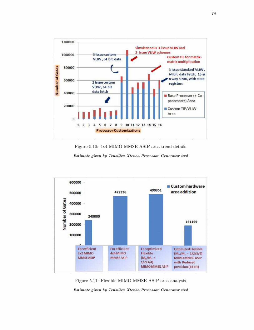
The graph in Figure 5.10 shows the area of base processor along with custom area

added for all the simulation cases we discussed earlier and highlighted in Figure 5.5.

The addition of VLIW and SIMD scheme shows many-fold increments in the area, as is

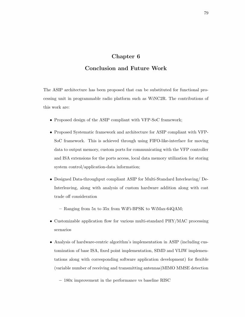
clearly visible. Similar trend can also be observed for 2x2 MIMO MMSE ASIP. Next we

combined the ASIP hardware for 4x4 and 2x2 application, so that now it can support

combinations of MR (1,2,3,4) and MT (1,2,3,4). The graph in Figure 5.11 shows the

hardware required for optimal implementation of ASIP for 2x2 MIMO MMSE appli-

cation, ASIP for 4x4 MIMO MMSE application, ASIP for MIMO MMSE application

for flexible number of MT and MR and ASIP with flexible MIMO MMSE application

with reduced precision (16 bit) processing respectively. The reduced precision has huge

impact on custom area since, all the register file widths are reduced by half. The in-

structions using these registers also use much lesser hardware due to lesser wide muxes,

multipliers, adders and decoding logic. This also gives us a motivation for future shift

towards 16 bit precision ASIP implementation.

5.4 Conclusion

As performance analysis indicate, the throughput requirement for 4x4 MIMO MMSE

application is not satisfied through this implementation. However, if a new matrix

inversion algorithm used, a considerable performance improvement can be acheieved

in order to achieve the goal of satisfying the throughput requirement. For 2x2 MIMO

MMSE application, the current implementation can satisfy the throughput with 6 and

72

12 sub-carriers. Again, for higher number of sub-carriers, we have to use more efficient

matrix inversion algorithm.

73

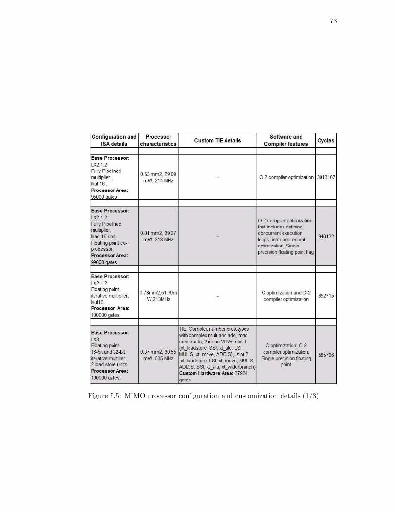
Figure 5.5: MIMO processor configuration and customization details (1/3)

74

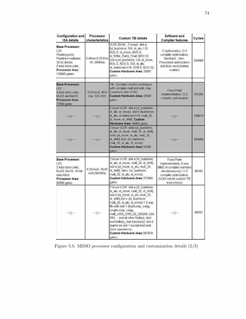
Figure 5.5: MIMO processor configuration and customization details (2/3)

75

Figure 5.5: MIMO processor configuration and customization details (3/3)

76

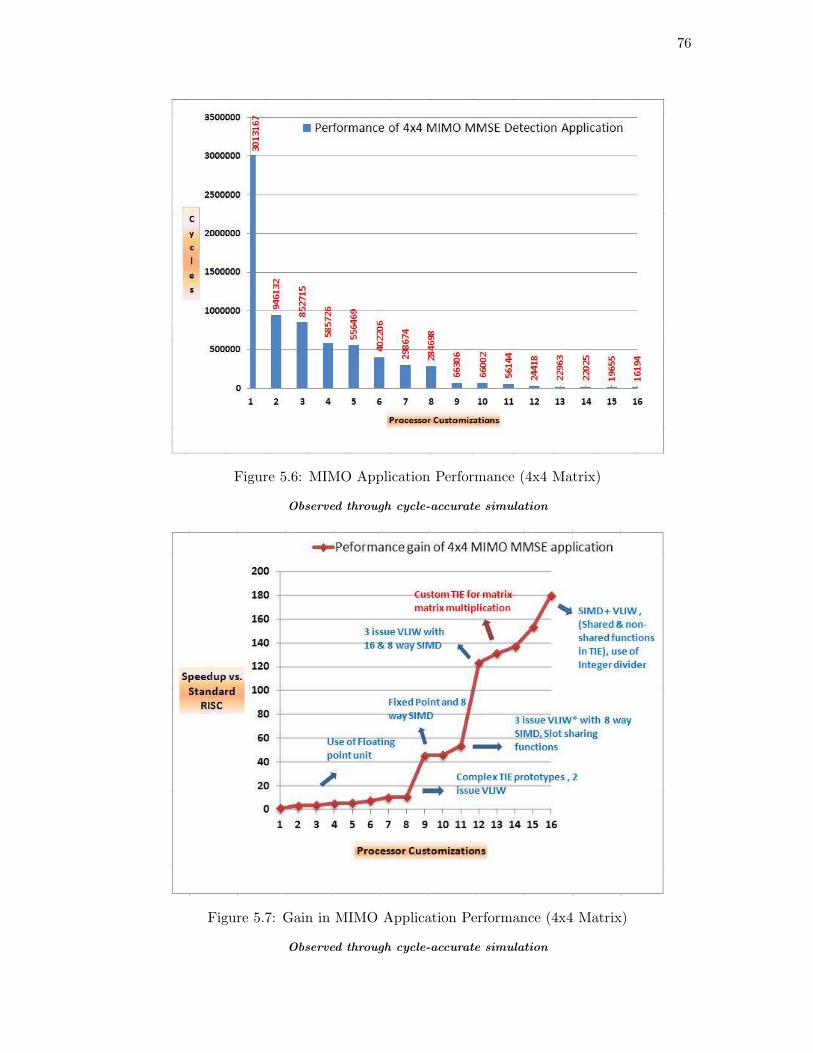
Figure 5.6: MIMO Application Performance (4x4 Matrix)

Observed through cycle-accurate simulation

Figure 5.7: Gain in MIMO Application Performance (4x4 Matrix)

Observed through cycle-accurate simulation

77

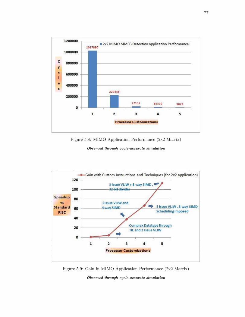
Figure 5.8: MIMO Application Performance (2x2 Matrix)

Observed through cycle-accurate simulation

Figure 5.9: Gain in MIMO Application Performance (2x2 Matrix)

Observed through cycle-accurate simulation

78

Figure 5.10: 4x4 MIMO MMSE ASIP area trend-details

Estimate given by Tensilica Xtensa Processor Generator tool

Figure 5.11: Flexible MIMO MMSE ASIP area analysis

Estimate given by Tensilica Xtensa Processor Generator tool

79

Chapter 6

Conclusion and Future Work

The ASIP architecture has been proposed that can be substituted for functional pro-

cessing unit in programmable radio platform such as WiNC2R. The contributions of

this work are:

• Proposed design of the ASIP compliant with VFP-SoC framework;

• Proposed Systematic framework and architecture for ASIP compliant with VFP-

SoC framework. This is achieved through using FIFO-like-interface for moving

data to output memory, custom ports for communicating with the VFP controller

and ISA extensions for the ports access, local data memory utilization for storing

system control/application-data information;

• Designed Data-throughput compliant ASIP for Multi-Standard Interleaving/ De-

Interleaving, along with analysis of custom hardware addition along with cost

trade off consideration

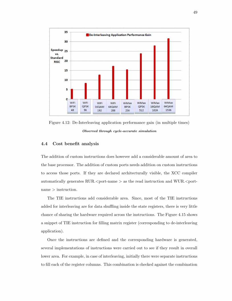
– Ranging from 5x to 35x from WiFi-BPSK to WiMax-64QAM;

• Customizable application flow for various multi-standard PHY/MAC processing

scenarios

• Analysis of hardware-centric algorithm’s implementation in ASIP (including cus-

tomization of base ISA, fixed point implementation, SIMD and VLIW implemen-

tations along with corresponding software application development) for flexible

(variable number of receiving and transmitting antennas)MIMO MMSE detection

– 180x improvement in the performance vs baseline RISC

80

6.1 Future work

The future work includes:

• Integrate Interleaver/De-Interleaver processor into WiNC2R platform

• Verify the interrupt /polling supporting scheme into the integrated chip

• Find out the context switching delays in the processor

• Find out more efficient algorithm for implementing MIMO MMSE detection on

ASIP. This also includes maintaining flexibility of the processor to support pro-

cessing for multiple number of transmitting/receiving antennas

• Investigate additional PHY functions suitable for ASIP

81

Glossary

ASIC Application Specific Integrated Circuit

ASIP Application Specific Instruction-set Processor

BPSC Bits Per Sub-Carrier

CBPS Coded Bits Per Symbol

CP Command Processor block in the WiNC2R

Processing Engine

CPI Cycles Per Instruction

CR Cognitive Radio

DSP Digital Signal Processor

EX / EXE Execute stage in a processor pipeline

FDG Field Delimiter Generator block in the

WiNC2R Processing Engine

FLIX Flexible Length Instruction Extensions

FU Functional Unit

GPP General Purpose Processor

GTT Global Task Table

IF Instruction Fetch stage in a processor pipeline

82

ISA Instruction Set Architecture

MIPS Million Instructions Per Second

MMSE Minimum Mean Square Error

MPSoC Multi-Processor System-on-Chip

PE Processing Engine

RISC Reduced Instruction Set Computer

RMAP Register Map

RTL Register Transfer Logic

SDR Software Defined Radio

SIMD Single Instruction Multiple Data

SoC System on Chip

TIE Tensilica Instruction Extension language

(used for adding custom instructions to the

Tensilica Xtensa base-line ISA)

TSP Task Spawn Processor block in the WiNC2R

Processing Engine

Verilog Hardware description language

VFP Virtual Flow Pipeline

VLIW Very Long Instruction Word

WiNC2R Winlab Network Centric Cognitive Radio

83

References

[1] Zoran Miljanic, Ivan Seskar, Khanh Le, and Dipankar Raychaudhuri. The WIN-LAB Network Centric Cognitive Radio Hardware Platform: WiNC2R. Mob. Netw.Appl., 13(5):533–541, 2008.

[2] Joe Evans, Gary Minden, and Ed Knightly. Technical document on cognitive radionetworks. Discussion papers, U.Kansas, Rice University, September 2006.

[3] Wireless Innovation Forum. What is Software Defined Radio. online, 2009.

[4] R.W. Thomas, L.A. DaSilva, and A.B. MacKenzie. Cognitive networks. In IEEEInternational Symposium on New Frontiers in Dynamic Spectrum Access Networks(DySPAN), 2005, pages 352 –360, 8-11 2005.

[5] Carlos R. Aguayo Gonzalez, Carl B. Dietrich, and Jeffrey H. Reed. Understandingthe Software Communications Architecture. Comm. Mag., 47(9):50–57, 2009.

[6] Qiwei Zhang, Andre B. J.Kokkeler, and Gerard J. M. Smit. Cognitive RadioDesign on an MPSoC Reconfigurable Platform. Mob. Netw. Appl., 13(5):424–430,2008.

[7] Muhammad Imran Anwar, Seppo Virtanen, and Jouni Isoaho. A Software DefinedApproach for Common Baseband Processing. Journal of System Archititecture,54(8):769–786, 2008.

[8] Yuan Lin, Hyunseok Lee, Mark Woh, Yoav Harel, Scott Mahlke, Trevor Mudge,Chaitali Chakrabarti, and Krisztian Flautner. SODA: A Low-Power Architecturefor Software Radio. In ISCA ’06: Proceedings of the 33rd annual internationalsymposium on Computer Architecture, pages 89–101, Washington, DC, USA, 2006.IEEE Computer Society.

[9] R. Baines and D. Pulley. Software Defined Baseband Processing for 3G Base Sta-tions. In 4th International Conference on 3G Mobile Communication Technologies,pages 123–127, 2003.

[10] Zoran Miljanic and Predrag Spasojevic. Resource Virtualization with Pro-grammable Radio Processing Platform. In WICON ’08: Proceedings of the 4thAnnual International Conference on Wireless Internet, pages 1–7, Brussels, Bel-gium, 2008. Institute for Computer Sciences, Social-Informatics and Telecommu-nications Engineering.

[11] Martin Grant. New Trends in Heterogenous Multi-core SOCs. Online, 2009.

[12] Lynley Gwennap. Single-Chip Control/Data Plane Processors: Trends, Features,Deployment. Technical report, The Linley Group, 2008.

84

[13] Jan Rabaey. Silicon Arhitectures for Wireless Systems - 1. Hotchips Tutorials atBerkeley Wireless Research Center, University of California, Berkeley, 2001.

[14] Andreas C. Doering and Silvio Dragone. Coupling a General Purpose Processorto an Application Specific Instruction Set Processor. US Patent:US 2008/0098202A1, April 2008.

[15] Kurt Keutzer, Sharad Malik, and A. Richard Newton. From ASIC to ASIP: TheNext Design Discontinuity. In ICCD’02: Proceedings of the 2002 IEEE Inter-national Conference on Computer Design: VLSI in Computers and Processors,page 84, Washington, DC, USA, 2002. IEEE Computer Society.

[16] Heinrich Meyr. System-on-Chip for Communications: The Dawn of ASIPs and theDusk of ASICs. In IEEE Workshop on Signal Processing Systems (SIPS), pages4–5, 2003. Seoul, Korea.

[17] Daniel Kastner. Compilation for Embedded Processors. European Summer Schoolon Embedded Systems, MRTC Report no 119/2004, 2003.

[18] Tensilica Inc. Xtensa LX3 Microprocessor Data Book. Tensilica Inc. LX3 productdocumentation, 2009.

[19] Tensilica Inc. The What, Why, and How of Configurable Processors. Tensilica Inc.White Paper, 2008.

[20] Shalini Jain. Hardware and Software for WiNC2R Cognitive Radio Platform.Master’s thesis, Rutgers University, October 2008.

[21] Sumit Satarkar. Performance Analysis of the WiNC2R Platform. Master’s thesis,Rutgers University, October 2009.

[22] Khanh Le and Tejaswy Hari. PE if spec.doc. WiNC2R Architecture SpecificationDocument, March 2010.

[23] S. Satarkar K. Le, S. Jain and T. Hari. WiNC2R Platform Functional Unit Archi-tecture. Architecture Specification Document, October 2008.

[24] Tensilica Inc. Tensilica Instruction Extension (TIE) Language Reference Manual.The Xtensa LX3 documentation, 2009.

[25] Mohit Wani. ten ProcessorCentric PE Architecture.vsd. WiNC2R ArchitectureSpecification Document, www.svn.winlab.rutgers.edu/cognitive, August 2009.

[26] John Hennessy and David Patterson. Computer Architecture: A Quantitative Ap-proach. Morgan Kauffmann, 2003.

[27] IEEE standards board. IEEE Std 802.11a-1999(R2003). IEEE, Piscataway, NJ,USA, June 2003.

[28] IEEE standards board. IEEE Standard 802.16-2004. IEEE, Piscataway, NJ, USA,October 2004.

85

[29] Eric Dell and Dake Liu. A Hardware Architecture for a Multi Mode Block Inter-leaver. In IEEE International Conference on Circuits and Systems for Communi-cations, 2004.

[30] Tensilica Inc. Area Efficient TIE Generation Using the Schedule Construct. Ten-silica application note, February 2009.

[31] A. Burg, S. Haene, D. Perels, P. Luethi, N. Felber, and W. Fichtner. Algorithmand VLSI Architecture for Linear MMSE Detection in MIMO-OFDM Systems. InProc. IEEE Int. Symp. on Circuits and Systems, 2006.

[32] Orthogonal Frequency Division Multiplexing. Wikipedia.

[33] Atif Raza Jafri, Amer Baghdadi, and Michel Jezequel. Rapid Prototyping ofASIP-based Flexible MMSE-IC Linear Equalizer. IEEE International Workshopon Rapid System Prototyping, 0:130–133, 2009.

[34] Mohit Wani. MIMO Fourth FixedPoint SIMD nf s44.tie. Custom Tie in-structions file for 4x4 MIMO MMSE detection, WiNC2R project onwww.svn.winlab.rutgers.edu/cognitive, June 2010.

[35] Mohit Wani. tenPE MIMO FixedPoint SIMD 5 s44.c. C Applica-tion for 2x2 MIMO MMSE detection on ASIP, WiNC2R project onwww.svn.winlab.rutgers.edu/cognitive, June 2010.

[36] Mohit Wani. MIMO Fourth FixedPoint SIMD nf s22.tie. Custom Tie in-structions file for 2x2 MIMO MMSE detection, WiNC2R project onwww.svn.winlab.rutgers.edu/cognitive, June 2010.

[37] Mohit Wani. tenPE MIMO FixedPoint SIMD 5 s22.c. C Applica-tion for 2x2 MIMO MMSE detection on ASIP, WiNC2R project onwww.svn.winlab.rutgers.edu/cognitive, June 2010.


Recommended