75
ATLAS 2D and 3D Device Simulator: Detailed Overview

ATLAS
2D and 3D Device Simulator: Detailed Overview

ATLAS 2D and 3D Device Simulator: Detailed Overview
Overview
Basic principles of device simulation
ATLAS Framework and Modules
Input/Output and Core processing
ATLAS input deck structure
Mesh design
Pisces Physical Models
Numerics
Tuning device simulators
3D simulations
- 2 -

ATLAS 2D and 3D Device Simulator: Detailed Overview
Basic Principles: What is ATLAS?
ATLAS is a 2D and 3D Device Simulation Framework
ATLAS solves the fundamental physical equations describing the dynamics of carriers in semiconductor devices for arbitrary device structures
ATLAS predicts terminal characteristics of semiconductor devices for steady state, transient, and small signal AC stimuli
ATLAS gives insight into the internal characteristics of semiconductor devices (e.g. carrier densities, fields, ionization/recombination rates, current densities etc.)
- 3 -

ATLAS 2D and 3D Device Simulator: Detailed Overview
Basic Principles: Create a Structure for Simulation
- 4 -

ATLAS 2D and 3D Device Simulator: Detailed Overview
Basic Principles: Create the Mesh
- 5 -

ATLAS 2D and 3D Device Simulator: Detailed Overview
Basic Principles: Define the Doping Profiles
- 6 -

ATLAS 2D and 3D Device Simulator: Detailed Overview
Elements of ATLAS Input Deck
- 7 -
Group
1. Structure Specification
2. Material Models Specification
3. Numerical Models Specification
4. Solution Specification
5. Results Analysis
Statements
MESHREGION
ELECTRODEDOPING
MATERIALMODELS
CONTACTINTERFACE
METHOD
LOGSOLVE
LOADSAVE
EXTRACTTONYPLOT

ATLAS 2D and 3D Device Simulator: Detailed Overview
ATLAS Inputs and Outputs
- 8 -
ATLAS
Device
Simulation
DevEdit Structure and
Mesh Editor
ATHENA
Process
Simulation
DeckBuild
Run Time
Environment
ATLAS
Device
Simulation
TonyPlot Visualization
Tool
Structure
File
Command
File
Runtime
Output
Solution
Files
Log
Files

ATLAS 2D and 3D Device Simulator: Detailed Overview
ATLAS Framework Architecture
- 9 -

ATLAS 2D and 3D Device Simulator: Detailed Overview
ATLAS Framework and Modules: S-Pisces
Drift-diffusion equation set
Full energy balance / hydrodynamic equations
Cartesian and cylindrical coordinate systems
DC, AC and Transient simulation domains
Extensive database of physical models
Impact ionization for device breakdown effects
Acceptor-like and Donor-like Trap dynamics
Able to accurately simulate the basic operation of MOS, bipolar, diode and power devices which contain silicon, silicon dioxide, polysilicon or metal regions.
- 10 -
ATLAS 2D and 3D Device Simulator: Detailed Overview
ATLAS Framework and Modules: Giga
Significant local heating can occur which affects terminal characteristics for example:
High current devices
Breakdown characteristics
SOI device simulation (Oxide is a good thermal insulator)
III-V devices (substrates are poor conductors)
Fully Coupled into Energy Balance Model 6 equation solver
Important to treat Energy balance and lattice heating effects together
- 11 -

ATLAS 2D and 3D Device Simulator: Detailed Overview
ATLAS Framework and Modules: Quantum
1D Schrodinger solver
Van Dort Correction Model
Hansch Correction Model
Quantum moments model
- 12 -

ATLAS 2D and 3D Device Simulator: Detailed Overview
ATLAS Framework and Modules: MixedMode
Embeds up to 10 ATLAS devices within a standard spice netlist and solves the complete system
ESD simulation of human body model and machine model specifications
SEU simulation of memory cells where the logical mode switches after an alpha particle strike
circuit analysis of devices with no accurate compact model for example certain power devices
verification of newly developed compact models
- 13 -

ATLAS 2D and 3D Device Simulator: Detailed Overview
ATLAS Framework and Modules: Luminous
General purpose 2D ray trace and photogeneration. Enables simulation of optoelectronic devices:
Photodectors, photoconductors, solar cells, CCDs, LEDs, etc.
Si-pased optoelectronic devices in conjunction with S-Pisces
Optoelectronic devices based on advanced material systems including heterostructures in conjunction with Blaze
Optical and self-heating effects (with Giga)
Optoelectronic device-circuit simulation (with MixedMode ray tracing algorithms
Allows simulation of anti-reflective coatings
- 14 -

ATLAS 2D and 3D Device Simulator: Detailed Overview
Mesh Design: Basic Guidelines
A good mesh is crucial to accurate simulation results.
Creating a good mesh is learned mainly from experience.
Some basic guidelines are to refine in key areas: Around junctions and depletion regions
Inversion regions
Areas of high electric field
Areas of current flow
Base region of BJTs
E-B junction is very critical
DevEdit is an ideal tool for creating and modifying the mesh only where the user wishes it
- 15 -

ATLAS 2D and 3D Device Simulator: Detailed Overview
Mesh Design: Basic Guidelines (con’t)
A suitable grid for process simulation may not be suitable for device simulation
In general, minimize the number of mesh points Solution time »k*(mesh points)1.5 –> 2.5
BUT... too few mesh points can take LONGER since each solution takes longer to converge. You cannot beat experience here
Use DevEdit to remove unnecessary mesh points and to concentrate the mesh where it’s needed
10Å mesh in inversion regions. Concentrate mesh at junctions
- 16 -

ATLAS 2D and 3D Device Simulator: Detailed Overview
Mesh Design: Effect on MOSFET Drain Current
Graph showing effect of increasing drain current with grid spacing
This shows the requirement for a grid density for the inversion region of 10Å typically
- 17 -

ATLAS 2D and 3D Device Simulator: Detailed Overview
Mesh Design: Effect on Current Gain of a BJT
- 18 -

ATLAS 2D and 3D Device Simulator: Detailed Overview
Mesh Design: Effect on Current Gain of a BJT
- 19 -

ATLAS 2D and 3D Device Simulator: Detailed Overview
Mesh Design: Effect on Current Gain of a BJT
- 20 -

ATLAS 2D and 3D Device Simulator: Detailed Overview
Mesh Design: Effect on Current Gain of a BJT
- 21 -

ATLAS 2D and 3D Device Simulator: Detailed Overview
Contact Definition
CONTACT statement is used to: set workfunctions for example N+/P+ POLY gate (MOSFETs)
Surface recombination velocity (BJT emitter)
contact slaving and voltage control (BJT dual base contacts)
Schottky contacts (MESFETs, pHEMTs, Diodes, etc)
floating contacts (EEPROMs)
switch to current boundary conditions (latchup)
lumped contact R, L and C
distributed contact resistance
- 22 -

ATLAS 2D and 3D Device Simulator: Detailed Overview
S-Pisces Physical Models: Which Model?
All simulation programs use a hierarchy of models from simple to complex models. These are key to accurate simulations
More complex models are generally: More complete description of the actual physics
Have physically based parameters
More predictive
- 23 -

ATLAS 2D and 3D Device Simulator: Detailed Overview
S-Pisces Physical Models: Which Model?
Why not just choose the most complex model each time? CPU time vs. accuracy gain whilst considering the goal of the simulation
Simpler model gives the same answer in many cases
More tuning parameters
- 24 -

ATLAS 2D and 3D Device Simulator: Detailed Overview
Device Simulation Models
Mobility Models
Recombination Models
Generation Models
Carrier Statistics
Energy Balance
Lattice Heating
Model choice tends to be technology specific as well as application specific. Recommendations will be given.
- 25 -

ATLAS 2D and 3D Device Simulator: Detailed Overview
Mobility Models: Which one?
Models describing separate physical effects can be combined together
Concentration dependence (CONMOB)
Concentration and temperature dependence (ANALYTIC, ARORA) uses local temperature in Giga
Carrier concentration dependence (CCSMOB)
Parallel electric field dependence (FLDMOB) velocity saturation
separate negative differential mobility model for GaAs (EVSATMOD=1)
Transverse electric field dependence (TASCH, WATT, SHIRAHATA) surface mobility
Integrated models (CVT, YAMAGUCHI, KLA.x)
- 26 -

ATLAS 2D and 3D Device Simulator: Detailed Overview
Recombination Model Hierarchy
Shockley-Read-Hall two carrier recombination used in almost all simulations
based on fixed lifetimes (SRH)
concentration dependent lifetimes (CONSRH and KLASRH)
trap assisted tunneling (TRAP.TUNNEL)
Auger three carrier recombination (AUGER and KLAAUG ) significant when carrier concentrations high
Optical recombination (OPTR) for direct band-gap materials
dominant recombination in GaAs
Surface Recombination at semiconductor/insulator interfaces (S.N, S.P)
at metal/semiconductor interfaces (SURF.REC)
Traps discrete bulk traps (TRAP statement)
interface traps (INTTRAP statement)
continuous trap density for non-crystalline materials (DEFECT statement)
- 27 -

ATLAS 2D and 3D Device Simulator: Detailed Overview
Generation Model Hierarchy
Impact Ionization required for any sort of breakdown voltage simulation
Selberrherr’s Model (IMPACT SELB)
Grant’s Model (IMPACT)
Crowell-Sze Model (IMPACT CROWELL)
Concannon (IMPACT N.CONCAN P.CONCAN)
Valdinoci Model (IMPACT VALDINOCI)
Toyabe Model (IMPACT TOYABE)
Band to Band Tunneling standard model with E (BBT.STD)
Klaassen’s model with E (BBT.KL)
narrow bandgap model (KAGUN KAGUP)
- 28 -

ATLAS 2D and 3D Device Simulator: Detailed Overview
Generation Model Hierarchy (con’t)
Fowler-Nordheim Tunneling (FNORD) tunneling through insulators
used in EEPROM erasing
Hot Carrier Injection (HEI, HHI) energetic carrier transport through thin insulators
used in EEPROM programming
Thermionic Emission (EMISS.xx) used to model transport across potential barriers at heterojunctions
- 29 -

ATLAS 2D and 3D Device Simulator: Detailed Overview
Carrier Statistics Models
Boltzmann statistics default
Fermi-Dirac statistics (FERMI) high concentration effects
Incomplete Ionization (INCOMP) for dopant freezeout
required for low temperature simulations
extra model for heavy dopants in silicon (IONIZ)
Band Gap Narrowing (BGN) important in heavily doped regions
critical for bipolar simulations
- 30 -

ATLAS 2D and 3D Device Simulator: Detailed Overview
Lattice Heating and Energy Balance Simulations
Lattice Heating activated by MODELS LAT.TEMP
Energy Balance activated by MODELS HCTE.EL HCTE.HO
Additional numerical techniques available
See Six Equation Solver Training for more details
- 31 -

ATLAS 2D and 3D Device Simulator: Detailed Overview
Recommended Physical Model Selections
Recommended physical models for MOS type FETs: MODELS SRH CVT BGN
Recommended physical models for BJTs, thyristors, etc: MODELS KLASRH KLAAUG KLA BGN
Also include impact ionization to model breakdown: IMPACT SELB
In general do not switch on a model unless it is really needed
- 32 -

ATLAS 2D and 3D Device Simulator: Detailed Overview
Numerical Methods for Isothermal Drift Diffusion
All numerics settings chosen on METHOD statement All structure/parameter specification must be before this statement
All solution specification must be after it
Fully Coupled Method solves for potential and carriers coupled (METHOD NEWTON)
recommended for all cases even including SOI simulations
De-Coupled method solves potential and carriers sequentially (METHOD GUMMEL)
faster for low current cases
Combined method (METHOD GUMMEL NEWTON) runs initial decoupled iterations and switches to coupled
GUM.INIT parameter controls the number of initial decoupled iterations
most robust (but slowest) method
- 33 -

ATLAS 2D and 3D Device Simulator: Detailed Overview
ATLAS Syntax Guide
Recommended numerical settings METHOD NEWTON MAXTRAP=10 CLIMIT=1E-4
- 34 -
ATLAS 2D and 3D Device Simulator: Detailed Overview
The Curvetracer: An Overview
Algorithm to enable ATLAS to trace out complex IV curves
Avoids user intervention in switching from voltage to current boundary conditions
Ideal method for simulating snapback
Improves simulation of breakdown
- 35 -

ATLAS 2D and 3D Device Simulator: Detailed Overview
The Curvetracer: Features
Dynamic Load Line Approach from “An Automatic Biasing Scheme for Tracing Arbitrarily Shaped IV Curves”, Goosens et al., IEEE Trans CAD 1994, Vol 13, pp. 310-317
Automatic boundary condition selection
Automatic selection of voltage/current step size
A single SOLVE statement can be used to trace entire curves
Only in DC mode. Transient and MixedMode already have similar capability
- 36 -

ATLAS 2D and 3D Device Simulator: Detailed Overview
The Curvetracer: A Load Line Approach
- 37 -

ATLAS 2D and 3D Device Simulator: Detailed Overview
The Curvetracer: Typical Applications
CMOS Latch-up
Snapback Effects
Breakdown Voltages
Second Breakdown
- 38 -

ATLAS 2D and 3D Device Simulator: Detailed Overview
The Curvetracer: Syntax Guide
A single command is used to trace an IV curve SOLVE CURVETRACE
The TRACE statement sets up the parameters for the curve trace
When viewing results in TonyPlot the INT.BIAS rather BIAS should be used as the voltage axis of the IV curve
- 39 -

ATLAS 2D and 3D Device Simulator: Detailed Overview
The Curvetracer: TRACE Parameters
- 40 -
CONTR.NAME is the name of the electrode to be ramped
STEP.INIT defines the initial voltage step on the ramped electrode
NEXT.RATIO specifies the factor used to increase the voltage step in areas on the IV curve away from turning points
MINCUR may be used to set a small current value above which the dynamic load line algorithm is used. Below this STEP.INT and NEXT.RATIO are used. Highly recommended
END.VAL is used to stop tracing if the voltage or current of ramped electrode equals or exceeds END.VAL
VOLT_CONT denotes that END.VAL is a voltage
CURR_CONT denotes that END.VAL is a current

ATLAS 2D and 3D Device Simulator: Detailed Overview
ATLAS Syntax Guide: Data Output
Two dimensional structure files use the syntax: OUTPUT EFIELD
SAVE OUTF=2D.STR
SOLVE OUTF=<filename>.str
All terminal characteristics are saved in logfiles: LOG OUTF=<filename>.str
To stop sending data to a logfile either QUIT or insert another LOG statement or use LOG OFF statement
- 41 -

ATLAS 2D and 3D Device Simulator: Detailed Overview
ATLAS Syntax Guide
Numerics: METHOD NEWTON CARRIERS=2 Use syntax for most cases
Use CARRIERS=0 for initial guesses
Use METHOD GUMMEL NEWTON for devices with floating regions (e.g. SOI) This uses Gummel iterations to supply initial guess for Newton solver. It is more robust, but slower than regular Newton.
Contents of method statement statement vary with solution type GUMMEL DAMPED
Newton AUTONR
Always TRAP
- 42 -

ATLAS 2D and 3D Device Simulator: Detailed Overview
Sources of Error in Device Simulation
Inaccurate doping profiles
Insufficient physics
Unknown or inaccurate material parameters
Inaccurate model parameters
Reliance on empirically fitted models
Mesh induced errors
External effects
- 43 -

ATLAS 2D and 3D Device Simulator: Detailed Overview
Solving Doping Profile Errors
This is the largest source of error for ‘small geometry devices’ Apply correction to doping if using SRP results
Use a process simulator
Account for CD biasing in mask edge locations
For further information see “Calibrating Process Simulators”
- 44 -

ATLAS 2D and 3D Device Simulator: Detailed Overview
Solving Material Parameter Errors
Silicon parameters generally well-tuned already
For non-silicon materials, all parameters are subject to tuning
Some parameters are substrate dependent and MUST be tuned e.g. minority carrier lifetime
Some parameters are process dependent e.g. Qss
- 45 -

ATLAS 2D and 3D Device Simulator: Detailed Overview
Solving Model Parameter Errors
Remember that most models are empirically fitted to a particular set of data
Should be used only after other errors are handled
Most common parameters used are VSAT for saturation region tuning and Impact Ionization parameters for breakdown
- 46 -
ATLAS 2D and 3D Device Simulator: Detailed Overview
Solving Mesh Errors
Avoid obtuse triangles in the current path or high field areas
Avoid discontinuities in mesh density
Ensure adequate mesh density in high field areas
- 47 -

ATLAS 2D and 3D Device Simulator: Detailed Overview
External Effects
You are trying to compare measured data so you must understand your measurement system. The simulation is of a ‘perfect intrinsic device structure.”
External resistances Long tracks in street structures, substrate contacts
Temperature. Simulator uses 300K. Do you?
Test systems use transients. Can be important for some device effects
Variations in measured data. Best to tune to a curve of data rather that a single point.
Ensure extraction technique is the same e.g at least 4 ways to get MOS Vt
- 48 -

ATLAS 2D and 3D Device Simulator: Detailed Overview
How to Tune Device Simulators
Problem too many parameters to change
Run many simulations slow and tedious
Use Optimizer easier, but may not converge in difficult cases
User VWF using parameterized input decks
- 49 -

ATLAS 2D and 3D Device Simulator: Detailed Overview
How to Tune Device Simulators (con't.)
Tactic Eliminate or account for external effects
Measure what you can first to eliminate variables in the tuning
Thoroughly check all process related information
Use ‘unknown’ material parameters first
Use ‘major’ model parameters such as VSAT
- 50 -

ATLAS 2D and 3D Device Simulator: Detailed Overview
Lattice Heating Simulations
Wachutka’s model of lattice heating accounts for Joule heating
Heating/cooling from generation and recombination
Peltier and Thomson heating
Lattice heating is required for many reasons High power devices
ESD protection devices
SOI device operation
III-V material systems
Bipolar carrier injection processes
Accurate impact ionization
External heat sources
- 51 -

ATLAS 2D and 3D Device Simulator: Detailed Overview
Tuning Lattice Heating Simulations
There are four additional calibration requirements when simulating lattice heat flow
1. Temperature dependent physical models
2. Temperature dependent thermal conductivities
3. Temperature dependent heat capacities
4. Thermal boundary conditions
Tactic choose correct models 1
control material heating by 2
transient heat flow control with 3
apply external heat sources/sinks 4
- 52 -

ATLAS 2D and 3D Device Simulator: Detailed Overview
Energy Balance Simulations
Energy balance simulations are required for today’s technologies: Deep sub-micron CMOS transistors
Advanced high mobility materials
Accurate substrate current modeling
Velocity overshoot effects
Gate leakage currents
Transconductance modeling
Nonlocal transport phenomena
Reference: Simulation Standard article, Volume 6, Number 4, April 1995.
- 53 -

ATLAS 2D and 3D Device Simulator: Detailed Overview
Tuning Energy Balance Equations
The relaxation times of the energy balance equations are the critical parameter but are difficult to measure.
1. Energy relaxation times
2. Energy dependent mobilites
3. temperature dependence of relaxation times
4. Energy dependent impact ionization
Tactic apply previous drift-diffusion calibration strategies
modify 1 to control velocity overshoot
2 is then coupled to 1
3 is uncharacterized but implemented for research purposes
specify energy relaxation length for 4
- 54 -

ATLAS 2D and 3D Device Simulator: Detailed Overview
Examples of Calibration Parameters
Threshold Voltage Gate workfunction (WORKF) CONTACT Surface states (QF) INTERFACE
Subthreshold Slopes
Surface states (QF) INTERFACE Interface defect traps INTTRAP Discrete Bulk defect traps TRAP Distributed bandgap defect traps DEFECTS
Theta
Physical models (MOS) MODELS Mobility equations coefficients (DELTAN.CVT) MOBILITY
Bipolar Gain
Physical models (BIPOLAR) MODELS Mobility equations coefficients (MUN, MUP) MOBILITY Recombination coefficients (TAUN0) MATERIAL Extrinsic resistances (RESISTANCE) CONTACT Surface recombination (SURF.REC) CONTACT
- 55 -

ATLAS 2D and 3D Device Simulator: Detailed Overview
Examples of Calibration Parameters (con't.)
I - V Curves Physical models (MOBILITY, BGN) MODELS Mobility equations coefficients (VSAT) MOBILITY
Leakage Currents Physical models (TUNNELING) MODELS Recombination coefficients (TAUN0) MATERIAL Trap density ( see subthreshold slope)
Breakdown Current level (Vt, Theta, Gain, etc) Impact ionization coefficients (SELB, AN1, BN1) IMPACT
EPROM Write/ Erase Floating contacts (FLOATING) CONTACT Physical models (PROGRAM, ERASE) MODELS Tunneling equation coefficients (IG. ELINR) MODELS Coupling capacitances CONTACT
- 56 -

ATLAS 2D and 3D Device Simulator: Detailed Overview
Examples of Calibration Parameters (con’t)
Lattice Heating Physical models (LAT.TEMP) MODELS Thermal conductivities (TC.A, TC.B, TC.C) MATERIAL Heat capacities coefficients (HC.A, HC.B, HC.C) MATERIAL Thermal boundary conditions THERMCONTACT
Energy Balance Physical model (HCTE) MODELS Relaxation times (TAUREL.EL) MATERIAL Impact ionization coefficients (LREL.EL) IMPACT
- 57 -

3D Device Simulation with ATLAS

ATLAS 2D and 3D Device Simulator: Detailed Overview
3D Device Simulation Modules in ATLAS
Device3D - Drift diffusion simulator with standard 2D models available
Blaze3D - III-V and II-VI simulator
Giga3D - Self-consistent lattice heat flow solution
MixedMode3D - Missed Spice and Device 3D simulation
Quantum3D - Quantum correction theory in 3D
TFT3D - Amorphous Poly Device simulation
Thermal3D - Heat dissipation only simulator
- 59 -

ATLAS 2D and 3D Device Simulator: Detailed Overview
Device 3D - 3D Silicon Device Simulator
Solves Poisson’s and electron/hole continuity equations
Prismatic based mesh structures
dc, ac and transient analysis modes
Choice of numerical solvers
Comprehensive physical models mobility
recombination
generation
carrier statistics
R, L and C lumped elements
C-interpreter functionality
- 60 -

ATLAS 2D and 3D Device Simulator: Detailed Overview
3D Device Simulation
Giga 3D Giga 3D contains most the functionality of the 2D Giga but works with the 3D products
This allows modeling of heatflow and self heating effects in 3D devices
The only functionality not supported in this version of Giga 3D that is supported in 2D is the BLOCK method
- 61 -

ATLAS 2D and 3D Device Simulator: Detailed Overview
Lattice Heating in 3D Using Giga3D
Isosurfaces of temperature in a power diode with current crowding into the anode
- 62 -

ATLAS 2D and 3D Device Simulator: Detailed Overview
3D Device Simulation
MixedMode3D This improvement allows simulation of 3D devices embedded in lumped element circuits
MixedMode3D contains all the functionality of 2D MixedMode simulator
- 63 -
ATLAS 2D and 3D Device Simulator: Detailed Overview
MixedMode3D
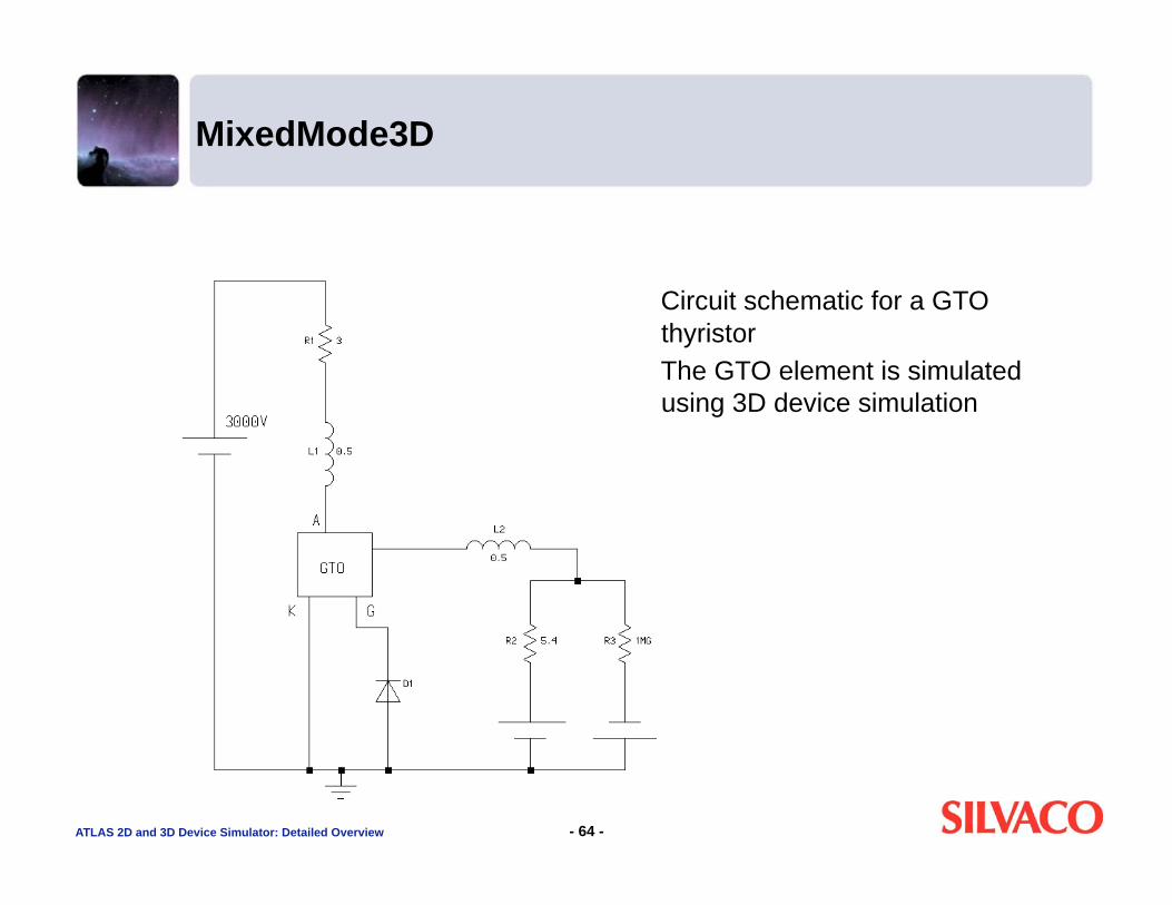
Circuit schematic for a GTO thyristor
The GTO element is simulated using 3D device simulation
- 64 -

ATLAS 2D and 3D Device Simulator: Detailed Overview
MixedMode3D
Currents in the GTO thyristor during turn-off through external circuit
- 65 -

ATLAS 2D and 3D Device Simulator: Detailed Overview
SEU in Memory Cell Using MixedMode3D
Voltage drop on mode of SRAM cell during single event upset
Circuit boundary conditions are required to model the cell behavior
3D device simulation is required to model the SEU
- 66 -

ATLAS 2D and 3D Device Simulator: Detailed Overview
3D Device Simulation
Blaze 3D This version accounts for spatial variations in bandgap due to variations in material composition in 3D This version supports all the same models as are supported in 2D Blaze with the exception of thermionic emission at heterojunctions and energy transport
This version also does not support compositional variation in the z direction
- 67 -

ATLAS 2D and 3D Device Simulator: Detailed Overview
HBT in Blaze3D
3D super self aligned SiGe HBT structure created and meshed using DevEdit3D
Emitter and base contacts are polysilicon
A section of oxide isolation is removed from the view to reveal the confined SiGe base region with denser mesh
- 68 -

ATLAS 2D and 3D Device Simulator: Detailed Overview
HBT in Blaze3D
(a) cut plane through 3D HBT structure at onset of avalanche breakdown. Note the concentration of impact ionization in the center of the n-SiGe collector extension region.
(b) HBT collector breakdown characteristic. (c) cut line through 2D section showing graph of impact ionization rate with depth under poly emitter stripe.
- 69 -

ATLAS 2D and 3D Device Simulator: Detailed Overview
HEMT in Blaze3D
2D cut plane taken from a Blaze3D solution for the 3D HEMT during a negative gate bias transient
The section is along the major axis of the resistive T-gate and shows the potential gradient along its length
The channel conduction (particularly the parasitic conduction in the AlGaAs) is consistent with the gate potential profile
- 70 -

ATLAS 2D and 3D Device Simulator: Detailed Overview
3D Device Simulation
TFT 3D This model allows modeling of poly and amorphous semiconductor devices such as TFTs in 3D
This model has all the functionality of the 2D TFT simulator
- 71 -

ATLAS 2D and 3D Device Simulator: Detailed Overview
TFT 3D
3D device simulation of high performance TFT device
- 72 -

ATLAS 2D and 3D Device Simulator: Detailed Overview
3D Device Simulation
Quantum3D This allows modeling of the effects of quantum confinement using the quantum moment approach
This model has all the functionality of the 2D Quantum model
- 73 -

ATLAS 2D and 3D Device Simulator: Detailed Overview
SEU in Device 3D
More control parameters for radial distribution and transient intensity of SEU pulses have been added
- 74 -

ATLAS 2D and 3D Device Simulator: Detailed Overview
SEU in MixedMode3D
Effect of an alpha particle strike on an inverter circuit simulated with MixedMode 3D
The memory bits are seen to switch during the event
Data corruption such as this could cause critical failure of the circuit
- 75 -


